

Philips NE570NB, NE570D, NE571N, NE571F, NE571D Datasheet
...
SA571
Compandor
Product specification 1997 Aug 14
INTEGRATED CIRCUITS
IC17 Data Handbook
Philips Semiconductors Product specification
SA571Compandor
2
1997 Aug 14 853-0812 18285
DESCRIPTION
The SA571 is a versatile low cost dual gain control circuit in which
either channel may be used as a dynamic range compressor or
expandor. Each channel has a full-wave rectifier to detect the
average value of the signal, a linerarized temperature-compensated
variable gain cell, and an operational amplifier.
The SA571 is well suited for use in cellular radio and radio
communications systems, modems, telephone, and satellite
broadcast/receive audio systems.
FEA TURES
•Complete compressor and expandor in one IChip
•T emperature compensated
•Greater than 110dB dynamic range
•Operates down to 6VDC
•System levels adjustable with external components
•Distortion may be trimmed out
•Dynamic noise reduction systems
•Voltage-controlled amplifier
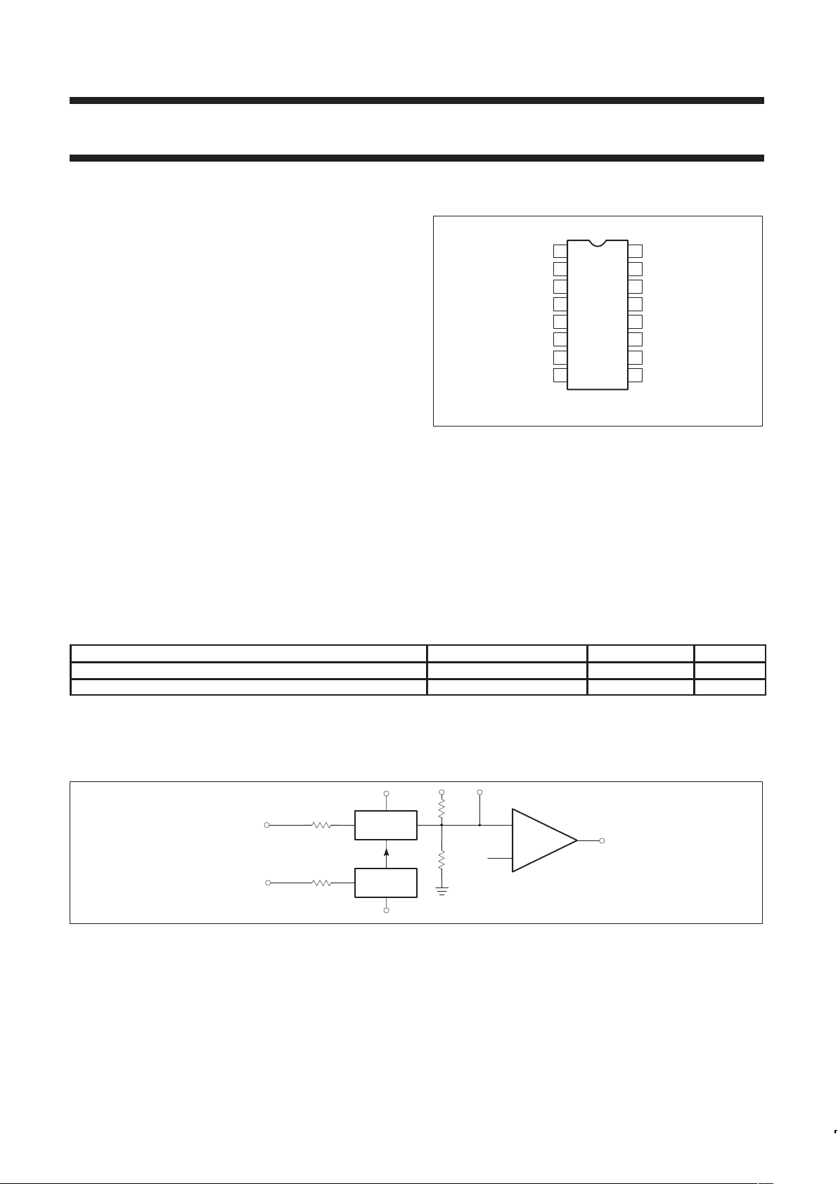
PIN CONFIGURATION
RECT CAP 1
RECT IN 1
AG CELL IN 1
GND
RECT CAP 2
AG CELL IN 2
RECT IN 2
V
CC
D, and N Packages
1
1
2
3
4
5
6
7
8
9
10
11
12
13
14
16
15
INV. IN 1
RES. R
3
1
OUTPUT 1
THD TRIM 1
INV. IN 2
RES. R3 2
OUTPUT 2
THD TRIM 2
TOP VIEW
NOTE:
1. SOL - Released in Large SO Package Only.
SR00675
Figure 1. Pin Configuration
APPLICATIONS
•Cellular radio
•High level limiter
•Low level expandor—noise gate
•Dynamic filters
•CD Player
ORDERING INFORMATION
DESCRIPTION TEMPERATURE RANGE ORDER CODE DWG #
16-Pin Plastic Small Outline Large (SOL) -40 to +85°C SA571D SOT162-1
16-Pin Plastic Dual In-Line Package (DIP) -40 to +85°C SA571N SOT38-4
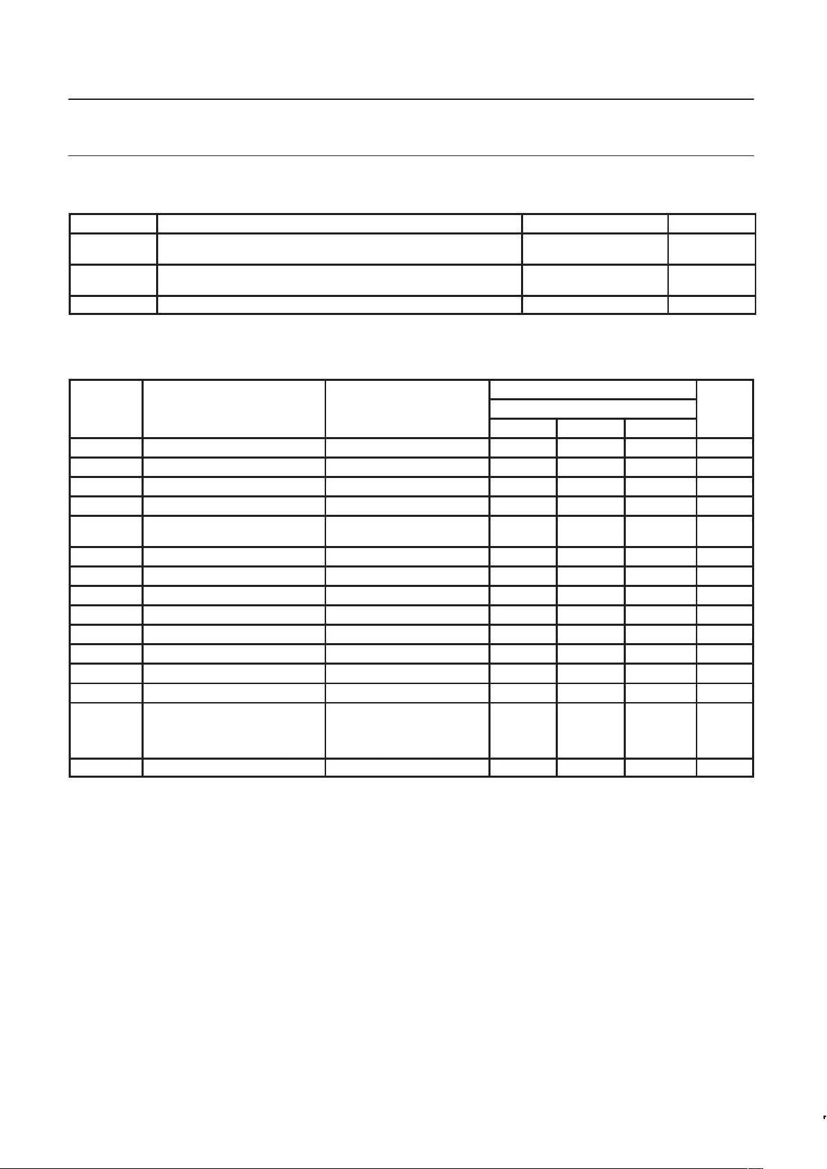
BLOCK DIAGRAM
VARIABLE
GAIN
∆G IN
RECT IN
V
REF
THD TRIM
R2 20k
R1 10k
RECT CAP
R3
R3 20k
R4 30k
1.8V
INVERTER IN
OUTPUT
+
–
RECTIFIER
SR00676
Figure 2. Block Diagram
Philips Semiconductors Product specification
SA571Compandor
1997 Aug 14
3
ABSOLUTE MAXIMUM RATINGS
SYMBOL PARAMETER RATING UNITS
V
CC
Maximum operating voltage
571
18
VDC
T
A
Operating ambient temperature range
SA
-40 to +85
°C
P
D
Power dissipation 400 mW
AC ELECTRICAL CHARACTERISTICS
VCC = +6V, TA = 25°C; unless otherwise stated.
LIMITS
SYMBOL PARAMETER TEST CONDITIONS SA571
5
UNITS
MIN TYP MAX
V
CC
Supply voltage 6 18 V
I
CC
Supply current No signal 3.2 4.8 mA
I
OUT
Output current capability ±20 mA
SR Output slew rate ±.5 V/µs
Gain cell distortion
2
Untrimmed
Trimmed
0.5
0.1
2.0 %
Resistor tolerance ±5 ±15 %
Internal reference voltage 1.65 1.8 1.95 V
Output DC shift
3
Untrimmed ±30 ±150 mV
Expandor output noise No signal, 15Hz-20kHz
1
20 60 µV
Unity gain level
6
1kHz -1.5 0 +1.5 dBm
Gain change
2, 4
±0.1 dB
Reference drift
4
+2, -25 +20, -50 mV
Resistor drift
4
+8, -0 %
Tracking error (measured relative to
value at unity gain) equals [V
O
- V
O
(unity gain)] dB - V2dBm
Rectifier input,
V
2
= +6dBm, V1 = 0dB
V2 = -30dBm, V1 = 0dB
+0.2
+0.2 -1, +1.5
dB
Channel separation 60 dB
NOTES:
1. Input to V
1
and V2 grounded.
2. Measured at 0dBm, 1kHz.
3. Expandor AC input change from no signal to 0dBm.
4. Relative to value at T
A
= 25°C.
5. Electrical characteristics for the SA571 only are specified over -40 to +85°C temperature range.
6. 0dBm = 775mV
RMS
.
Philips Semiconductors Product specification
SA571Compandor
1997 Aug 14
4
CIRCUIT DESCRIPTION
The SA571 compandor building blocks, as shown in the block
diagram, are a full-wave rectifier, a variable gain cell, an operational
amplifier and a bias system. The arrangement of these blocks in the
IC result in a circuit which can perform well with few external
components, yet can be adapted to many diverse applications.
The full-wave rectifier rectifies the input current which flows from the
rectifier input, to an internal summing node which is biased at V
REF
.
The rectified current is averaged on an external filter capacitor tied
to the C
RECT
terminal, and the average value of the input current
controls the gain of the variable gain cell. The gain will thus be
proportional to the average value of the input signal for
capacitively-coupled voltage inputs as shown in the following
equation. Note that for capacitively-coupled inputs there is no offset
voltage capable of producing a gain error. The only error will come
from the bias current of the rectifier (supplied internally) which is
less than 0.1µA.
G
|V
IN
V
REF
|avg
R
1
or
G
|V
IN
|avg
R
1
The speed with which gain changes to follow changes in input signal
levels is determined by the rectifier filter capacitor. A small capacitor
will yield rapid response but will not fully filter low frequency signals.
Any ripple on the gain control signal will modulate the signal passing
through the variable gain cell. In an expander or compressor
application, this would lead to third harmonic distortion, so there is a
trade-off to be made between fast attack and decay times and
distortion. For step changes in amplitude, the change in gain with
time is shown by this equation.
G(t) (G
initial
G
final
)e t
G
final
; 10k x C
RECT
The variable gain cell is a current-in, current-out device with the ratio
I
OUT/IIN
controlled by the rectifier. IIN is the current which flows from
the ∆G input to an internal summing node biased at V
REF
. The
following equation applies for capacitively-coupled inputs. The
output current, I
OUT
, is fed to the summing node of the op amp.
I
IN
V
IN
V
REF
R
2
V
IN
R
2
A compensation scheme built into the ∆G cell compensates for
temperature and cancels out odd harmonic distortion. The only
distortion which remains is even harmonics, and they exist only
because of internal offset voltages. The THD trim terminal provides
a means for nulling the internal offsets for low distortion operation.
The operational amplifier (which is internally compensated) has the
non-inverting input tied to V
REF
, and the inverting input connected to
the ∆G cell output as well as brought out externally. A resistor, R
3
, is
brought out from the summing node and allows compressor or
expander gain to be determined only by internal components.
The output stage is capable of ±20mA output current. This allows a
+13dBm (3.5V
RMS
) output into a 300Ω load which, with a series
resistor and proper transformer, can result in +13dBm with a 600 Ω
output impedance.
A bandgap reference provides the reference voltage for all summing
nodes, a regulated supply voltage for the rectifier and ∆G cell, and a
bias current for the ∆G cell. The low tempco of this type of reference
provides very stable biasing over a wide temperature range.
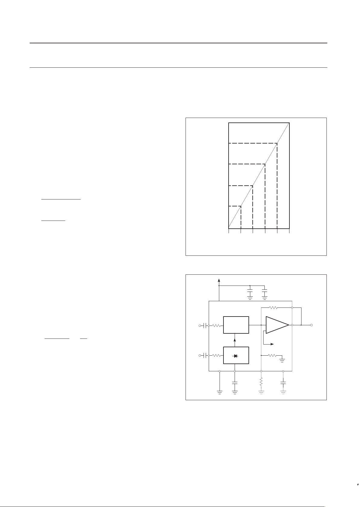
The typical performance characteristics illustration shows the basic
input-output transfer curve for basic compressor or expander
circuits.
+20
+10
0
–10
–20
–30
–40
–50
–60
–70
–80
–40 –30 –20 –10 0 +10
COMPRESSOR OUTPUT LEVEL
OR
EXPANDOR INPUT LEVEL (dBm)
COMPRESSOR INPUT LEVEL OR EXPANDOR OUTPUT LEVEL (dBm)
SR00677
Figure 3. Basic Input-Output Transfer Curve
TYPICAL TEST CIRCUIT
20k
10k
13
3.14
2.2
2.15
4 1.16
2.2
5.12
8.2k
8.9
200pF
30k
20k
7.10
6.11
V
1
V
2
V
O
VCC = 15V
V
REF
∆G
10µF
0.1µF
2.2µF
SR00678
Figure 4. Typical Test Circuit
INTRODUCTION
Much interest has been expressed in high performance electronic
gain control circuits. For non-critical applications, an integrated
circuit operational transconductance amplifier can be used, but
when high-performance is required, one has to resort to complex
discrete circuitry with many expensive, well-matched components.
 Loading...