


Philips FM242 AA Service Manual
Colour Television Chassis
FM242
AA
Contents Page Contents Page
1 Technical Specifications, Connections, and 2
Chassis Overview
2 Safety Instructions, Maintenance, Warnings, 5
and Notes
3 Directions for Use 7
4 Mechanical Instructions 10
5 Service Modes, Error Codes, Fault Finding, 13
and Repair Tips
6 Block Diagrams, Test Point Overviews, and Wiring
Diagram
Block Diagram Video 19
Block Diagram Audio 20
Power Lines Overview 21
2
I
C-IC Overview 22
Testpoint Overview Audio Amplifier 23
Testpoint Overview Power Supply 24
Testpoint Overview SCAVIO Panel 25
Wiring Diagram 26
7 Electrical Diagrams and PWB lay-outs Diagram PWB
Audio Amplifier: DC Protection (Diagram A1) 27 34-35
Audio Amplifier: Filters (Diagram A2) 28 34-35
Audio Amplifier: Left High (Diagram A3) 29 34-35
Audio Amplifier: Left Low (Diagram A4) 30 34-35
Audio Amplifier: Right High (Diagram A5) 31 34-35
Audio Amplifier: Right Low (Diagram A6) 32 34-35
Audio Amp: Supply + DC Prot. (Diagram A7) 33 34-35
LED/Switch Panel (Diagram LD) 36 37
SCAVIO: Function Blocks (Diagr. SC1) 38 53-62
SCAVIO: Sync Selection (Diagr. SC2) 39 53-62
SCAVIO: Video Select.ion (Diagr. SC3) 40 53-62
SCAVIO: Video ADC (Diagr. SC4) 41 53-62
SCAVIO: Video Select. Decoder (Diagr. SC5) 42 53-62
SCAVIO: VGA Input (Diagr. SC6) 43 53-62
SCAVIO: Control Functions 1 (Diagr. SC7) 44 53-62
©
Copyright 2003 Philips Consumer Electronics B.V. Eindhoven, The Netherlands.
All rights reserved. No part of this publication may be reproduced, stored in a
retrieval system or transmitted, in any form or by any means, electronic,
mechanical, photocopying, or otherwise without the prior permission of Philips.
SCAVIO: Control Functions 2 (Diagr. SC8) 45 53-62
SCAVIO: Scaler Clock Gen. (Diagr. SC9) 46 53-62
SCAVIO: PW Scaler + Memory (Diagr. SC10) 47 53-62
SCAVIO: Back-End EPLD (Diagr. SC11) 48 53-62
SCAVIO: Back-End LVDS Out (Diagr. SC12) 49 53-62
SCAVIO: Audio Source Select. (Diagr. SC13) 50 53-62
SCAVIO: Audio Processor (Diagr. SC14) 51 53-62
SCAVIO: Audio Delay Line (Diagr. SC15) 52 53-62
VGA Connector Panel (Diagr. VGA) 63 64-65
8 Electrical Alignments 67
9 Circuit Descriptions 70
List of Abbreviations 81
10 Spare Parts List 83
11 Revision List 90
Published by CO 0363 Service PaCE Printed in the Netherlands Subject to modification EN 3122 785 13400
EN 2 FM242 AA1.
Technical Specifications, Connections, and Chassis Overview
1. Technical Specifications, Connections, and Chassis Overview
1.1 Technical Specifications
1.1.1 Picture
Display : FHT plasma panel
Screen size : 42" (106 cm)
Resolution : 852 x 480 pixels
(pixel pitch
1.095 x 1.11 mm)
Contrast ratio : 1000 : 1
1.1.2 Sound
Maximum power : 30 Wrms (for version
with speakers)
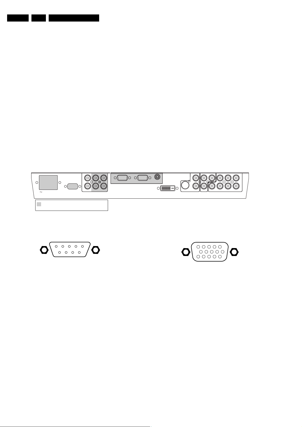
1.2 Connections
1.2.1 Rear Connections
AUDIO IN
L
R
MAINS
! AllFunctional blocksshaded greyarerequired for
the"BasicConfiguration".
Theremainderisrequiredforthe"EnhancedConfiguration".
RS323
DVI-D
VGA2 VGA1
1.1.3 Miscellaneous
VGA1 VGA2 RC-OUT
Mains voltage : 95 - 264 V
Mains frequency : 50/60 Hz
Ambient temperature : + 5 to + 40 deg. C
Maximum humidity : 90% R.H.
Power consumption : around 380 W
Standby Power consumption : < 2 W
Weight : 35 kg
Dimensions (WxHxD) : Speakered version:
1215 x 657 x 90 mm
: Speaker-less version:
1070 x 660 x 90 mm
DVI-D
Y/C S
SVHS
AV2 AV1
L
R
AUDIOINAUDIO
CVBSB/Pb/Cb
IN
H
L
AV3
B/Pr/Cr
CL 16532099_010.eps
R
v
AUDIO
IN
260801
Figure 1-1 Rear Connections
RS232
1
6
5
9
Figure 1-2 RS232 connector (subD-9p)
1-
2 - TXD (UART)
3 - RXD (UART)
4 - RL_ICN (ICONN)
5 - Ground
6 - GL_ICN (ICONN)
7 - LD_ICN (ICONN)
8 - IR_TX (ICONN)
9 - IR_RX (ICONN)
10 - Ground
11 - Ground
Audio - In (DVI-D)
1 - Audio - L 0.5 Vrms / 1 kΩ
2 - Audio - R 0.5 Vrms / 1 kΩ
Audio - In (VGA2)
1 - Audio - L 0.5 Vrms / 1 kΩ
2 - Audio - R 0.5 Vrms / 1 kΩ
VGA1 - In
1
6
11
5
10
15
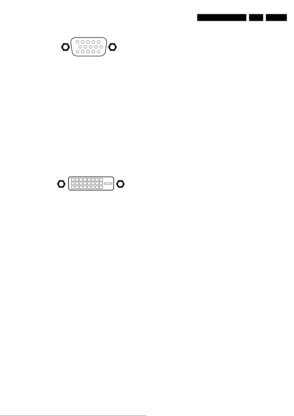
Figure 1-3 VGA Connector
1 - Red 0.7 Vpp / 75 Ω
2 - Green 0.7 Vpp / 75 Ω
3 - Blue 0.7 Vpp / 75 Ω
4-TXD
5 - Ground
6 - Red Ground
7 - Green Ground
8 - Blue Ground
9-RC
10 - Ground
11 - RXD
12 - DDC_SDA
13 - H-sync 0 - 5 V
14 - V-sync 0 - 5 V
15 - DDC_SCL
Audio - In (VGA1)
1 - Audio - L 0.5 Vrms / 1 kΩ
2 - Audio - R 0.5 Vrms / 1 kΩ
Technical Specifications, Connections, and Chassis Overview
EN 3FM242 AA 1.
VGA2 - Out
1
6
11
5
10
15
Figure 1-4 VGA Connector
1 - Red (0.7 Vpp/75 Ω)
2 - Green (0.7 Vpp/75 Ω)
3 - Blue (0.7 Vpp/75 Ω)
4-TXD
5 - Ground
6 - Red Ground
7 - Green Ground
8 - Blue Ground
9-
10 - Ground
11 - RXD
12 - DDC_SDA
13 - H-sync 0 - 5 V
14 - V-sync 0 - 5 V
15 - DDC_SCL
RC - Out
1-RC
DVI-D
18
916
17
C5
24
2 - Audio - L 0.5 Vrms / 10 kΩ
3 - Audio - R 0.5 Vrms / 10 kΩ
AV3: Audio/Video - In
1 - G/Y/Y 0.7 Vpp / 75 Ω
2 - B/Pb/Cb 0.7 Vpp / 75 Ω
3 - R/Pr/Cr 0.7 Vpp / 75 Ω
4-H
5-V
6 - Audio - L 0.5 Vrms / 10 kΩ
7 - Audio - R 0.5 Vrms / 10 kΩ
Figure 1-5 DVI-D Connector
1-RX2-
2-RX2+
3 - Ground
4-
5-
6 - DDC-SCL
7 - DDC-SDA
8-
9-RX1-
10 - RX1+
11 - Ground
12 -
13 -
14 - 5V_STBY_SW
15 - Ground
16 - 5V_STBY_SW
17 - RX0-
18 - RX0+
19 - Ground
20 -
21 - Ground
22 -
23 - RXC+
24 - RXC-
C5- Ground
AV2: SVHS - In
1 - Y Ground
2 - C Ground
3 - Y 1 Vpp / 75 Ω
4 - C / 16:9 0.3 Vpp / 75 Ω
AV2: Audio - In
1 - Audio - L 0.5 Vrms/10 kΩ
2 - Audio - R 0.5 Vrms/10 kΩ
AV1: Audio/Video - In
1 - CVBS 1 Vpp / 75 Ω
EN 4 FM242 AA1.
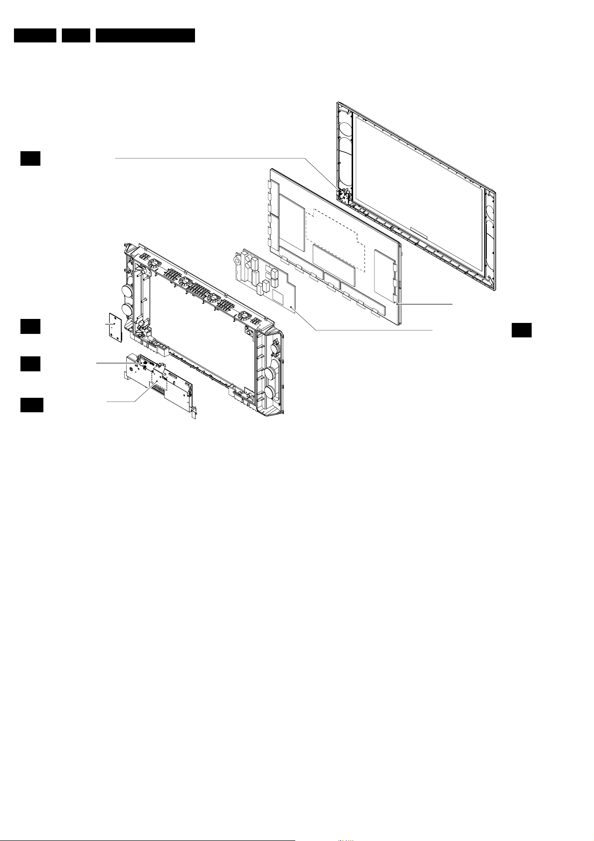
1.3 Chassis Overview
LED / SWITCH PANEL
LD
Technical Specifications, Connections, and Chassis Overview
Y-
Buffer
(up)
Y-Main
Y-
Buffer
(down)
A
SC
VGA
AUDIO AMPLIFIER
PANEL
SCAVIO PANEL
VGA CONNECTOR
PANEL
Logic-Buffer (E
)
SMPS
Figure 1-6 PWB Location
Logic Board
Logic-
B
uffer (F)
Logic-Buffer (G
X- Board
)
PLASMA DISPLAY PANEL
POWER SUPPLY PANEL
CL 36532011_010.eps
P
060303

Safety Instructions, Warnings, and Notes
2. Safety Instructions, Warnings, and Notes
EN 5FM242 AA 2.
2.1 Safety Instructions
Safety regulations require that during a repair:
• Connect the set to the mains via an isolation transformer
(> 800 VA).
• Do not operate the monitor without the front glass plate.
One function of this glass plate is to absorb IR radiation.
Without this glass plate, the level of radiation could
damage your eyes.
• Replace safety components, indicated by the symbol
only by components identical to the original ones.
Safety regulations require that after a repair, the set must be
returned in its original condition. Pay, in particular, attention to
the following points:
• Route the wire trees correctly and fix them with the
mounted cable clamps.
• Check the insulation of the mains lead for external
damage.
• Check the electrical DC resistance between the mains plug
and the secondary side (only for sets which have a mains
isolated power supply):
1. Unplug the mains cord and connect a wire between the
two pins of the mains plug.
2. Set the mains switch to the 'on' position (keep the
mains cord unplugged!).
3. Measure the resistance value between the pins of the
mains plug and the metal shielding of the tuner or the
aerial connection on the set. The reading should be
between 4.5 MΩ and 12 MΩ.
4. Switch 'off' the set, and remove the wire between the
two pins of the mains plug.
• Check the cabinet for defects, to avoid touching of any
inner parts by the customer.
2.2 Warnings
• All ICs and many other semiconductors are susceptible to
electrostatic discharges (ESD ). Careless handling
during repair can reduce life drastically. Make sure that,
during repair, you are connected with the same potential as
the mass of the set by a wristband with resistance. Keep
components and tools also at this same potential.
Available ESD protection equipment:
– Complete kit ESD3 (small tablemat, wristband,
connection box, extension cable and earth cable) 4822
310 10671.
– Wristband tester 4822 344 13999.
• Be careful during measurements in the high voltage
section.
• Never replace modules or other components while the unit
is switched 'on'.
• When you align the set, use plastic rather than metal tools.
This will prevent any short circuits and the danger of a
circuit becoming unstable.
2.3 Notes
• Clean the glass plate in front of the plasma display with a
slightly humid cloth. If, due to circumstances, there is some
dirt between the glass plate and the plasma display, this
must be cleaned by a qualified service engineer (see
section “Mechanical Instructions”).
• Measure the direct voltages and oscillograms with regard
to the chassis ground (), or hot ground () as this is
called.
• The direct voltages and oscillograms shown in the
diagrams are indicative. Measure them in the Service
Default Mode (see section “Service Modes”).
,
• Where necessary, measure the voltages in the power
supply section both in normal operation () and in standby
(). These values are indicated by means of the
appropriate symbols.
• The semiconductors indicated in the circuit diagram and in
the parts lists, are interchangeable per position with the
semiconductors in the unit, irrespective of the type
indication on these semiconductors
2.3.1 Schematic Notes
• All resistor values are in ohms and the value multiplier is
often used to indicate the decimal point location (e.g. 2K2
indicates 2.2 kOhm).
• Resistor values with no multiplier may be indicated with
either an 'E' or an 'R' (e.g. 220E or 220R indicates 220
Ohm).
• All Capacitor values are expressed in Micro-Farads (µ =
-6
x10
), Nano-Farads (n = x10-9), or Pico-Farads (p = x10
12
).
• Capacitor values may also use the value multiplier as the
decimal point indication (e.g. 2p2 indicates 2.2 pF).
• An 'asterisk' (*) indicates component usage varies. Refer to
the diversity tables for the correct values.
• The correct component values are listed in the Electrical
Replacement Parts List. Therefore, always check this list
when there is any doubt.
2.3.2 Rework on BGA ICs
General
Although (LF)BGA assembly yields are very high, there may
still be a requirement for component rework. By rework, we
mean the process of removing the component from the PWB
and replacing it with a new component. If an (LF)BGA is
removed from a PWB, the solder balls of the component are
deformed drastically so the removed (LF)BGA has to be
discarded.
Device removal
As is the case with any component, it is essential when
removing an (LF)BGA that the board, tracks, solder lands, or
surrounding components are not damaged. To remove an
(LF)BGA, the board must be uniformly heated to a temperature
close to the reflow soldering temperature. A uniform
temperature reduces the chance of warping the PWB.
To do this, we recommend that the board is heated until it is
certain that all the joints are molten. Then carefully pull the
component off the board with a vacuum nozzle. For the
appropriate temperature profiles, see the IC data sheet.
Area preparation
When the component has been removed, the vacant IC area
must be cleaned before replacing the (LF)BGA.
Removing an IC often leaves varying amounts of solder on the
mounting lands. This excessive solder can be removed with
either a solder sucker or solder wick. The remaining flux can be
removed with a brush and cleaning agent.
After the board is properly cleaned and inspected, apply flux on
the solder lands and on the connection balls of the (LF)BGA.
Note: Do not apply solder paste, as this has shown to result in
problems during re-soldering.
-

EN 6 FM242 AA2.
Device replacement
The last step in the repair process is to solder the new
component on the board. Ideally, the (LF)BGA should be
aligned under a microscope or magnifying glass. If this is not
possible, try to align the (LF)BGA with any board markers.
To reflow the solder, apply a temperature profile according to
the IC data sheet. So as not to damage neighbouring
components, it may be necessary to reduce some
temperatures and times.
Safety Instructions, Warnings, and Notes
3. Directions for Use
Directions for Use
EN 7FM242 AA 3.
EN 8 FM242 AA3.
Directions for Use

Directions for Use
EN 9FM242 AA 3.
EN 10 FM242 AA4.
Mechanical Instructions
4. Mechanical Instructions
Index of this chapter:
• Service Position Monitor
• Rear Cover Removal
• Service Position Panels
• PDP and Glass Plate Replacement
• Re-assembly
Note: Figures below can deviate from the actual situation, due
to different set executions.
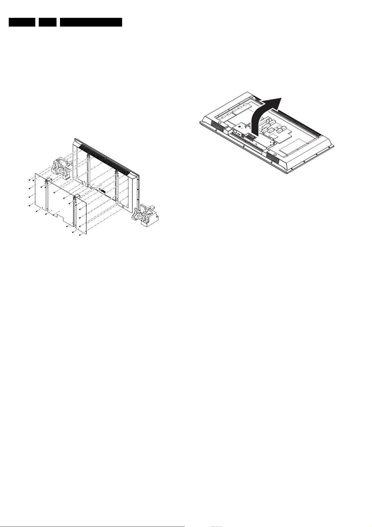
4.1 Service Position Monitor
Figure 4-1 Service Position
First, put the monitor in its service position. (Can be done via
buffers as showed on figure, but preferable via new service
position solution as described below. Still some improvising is
needed for service positions panels however). Therefore,
disconnect all cables connected to the monitor and take the
monitor of the wall (or tabletop stand). Then, fix the monitor to
the 2 service-poles. (the 2 poles together form a service-kit:
3122 785 90480; this service-stand can be used for 30” until
42” FTVs.
CL 16532099_041.eps
250901
4.3 Service Position Panels
4.3.1 SCAVIO Panel
Solder-side SCAVIO
B
CL 36532011_011.eps
Figure 4-2 Service position SCAVIO (1)
To access the panel:
1. Remove the cables from connectors 0320, 0305, 0301,
0319 and 0388 on the SCAVIO panel.
2. Remove the power cable from the mains power inlet to the
power supply (connector 0308).
3. Remove the five screws at the bottom of the SCAVIOpanel cover plate.
4. Hold the SCAVIO panel while removing the top screw, in
order to prevent that it will fall.
5. Take the panel out, and turn it 180 degrees, so that you
face the solder side of the SCAVIO panel.
6. Reconnect all cables. Use a standard power cable to
connect the mains directly to PSU-connector 0308, and
use the 'LED/Switch panel' service kit 3122 785 90410 (as
the original cable is too short).
Caution: When measuring, watch out for the 'hot' left heat sink
of the PSU!
200303
4.2 Rear Cover Removal
To be able to access or measure the panels, remove the rear
cover (metal back plate):
Warning: make sure that the mains power is disconnected
before you remove the metal back plate.
1. Remove all fixation screws of the back plate, as indicated
in the figure above (five at the top, five at each side, seven
at the bottom and the two larger ones just below the 'wall
mounting holes').
2. Remove the metal back plate. Make sure that wires and flat
foils are not damaged during plate removal.
Another way to measure the SCAVIO panel:
1. Remove the five screws at the bottom of the SCAVIOpanel cover plate.
2. Hold the SCAVIO panel while removing the top screw, in
order to prevent that it will fall.
3. Put a piece of paper (or cardboard) in front of the Power
Supply.
4. Take the panel out, and turn it upward [B], so that you face
the solder-side of the SCAVIO panel.
Caution: Make sure that the metal connector plate does not
touch any 'hot' part of the Power Supply (heatsink).

Mechanical Instructions
EN 11FM242 AA 4.
Component-side SCAVIO
CL 16532099_043.eps
250901
Figure 4-3 Service position SCAVIO (2)
To access the other side of the SCAVIO panel:
1. Disconnect all cables going to the SCAVIO panel.
2. Remove all screws at the connectors of the connector
plate, see figure 'Solder-side SCAVIO'.
3. Remove the three fixation screws that connect the SCAVIO
panel to the connector plate, see figure 'Component-side
SCAVIO'.
4. Reconnect the SCAVIO panel, be careful: do not make a
short-circuit!
4.3.4 Audio Amplifier Panel (only valid for “speaker”-version)
The solder-side of this panel is directly accessible. To access
the component-side, or to remove the whole panel, unscrew
the three fixation screws
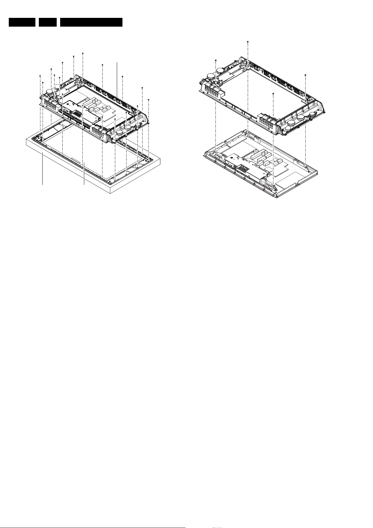
4.3.5 LED/Switch Panel and Speakers
Plastic backcover
Foam cushion
4.3.2 VGA Connector Panel
How to remove the VGA Connector panel:
1. Squeeze the plastic pins that attach this panel to the
SCAVIO board, while you pull it carefully upwards.
2. Unplug the flat foil cable.
4.3.3 Power Supply Panel
CL 36532011_021.eps
Figure 4-4 Remove PSU
The supply panel can not be repaired by the network. As
measure points are accessible for possible re-alignment, there
is no further service-position.
To remove the panel unscrew the 9 screws (see drawing) and
disconnect the cables.
200303
CL 36532011_012.eps
170303
Figure 4-5 Service Position LED/Switch Panel and Speakers
To access or replace the LED/Switch panel and/or speakers:
1. Take the monitor from its service stand, and put it (face
down) on a soft surface (blanket or foam cushion), to
make sure that you do not damage the front glass plate.
2. Unscrew all fixation screws of the plastic back cover: five at
all sides.
3. Lift and remove the plastic back cover.
4. You can access now the LED/Switch panel and/or the
speakers.
4.3.6 LED/Switch panel
To measure the component-side, or to remove the LED/Switch
panel, unscrew one fixation screw (see enlarged part of figure
'LED/Switch Panel and Speakers'), and remove the panel.
4.3.7 Loudspeakers (if valid)
When you have removed the plastic back cover, you must
replace the speaker-box sealing foams (12nc: 3122 358
76221). This, to ensure that the loudspeakers are airtight.
Do not stretch the foam during mounting. Pay special
attention to the corners, to make sure that the foam is not
stretched and that it is pushed into the corners.
EN 12 FM242 AA4.
4.4 PDP and Glass Plate Replacement
Shielding frame
Front displayFoam cushion
Figure 4-6 Exchange Glass Plate
To exchange the glass plate
1. Take the monitor from its service stand, and put it (face
down) on a soft surface (blanket or foam cushion), to make
sure that you do not damage the front glass plate.
2. Remove the metal back plate as described in paragraph
'Rear Cover Removal'.
3. Unscrew all fixation screws of the plastic back cover: four
at the left and right side, three at the bottom and top side.
4. Lift and remove the plastic back cover.
5. Unscrew two fixation screws of the triangular shaped cable
holder at the left bottom, see figure 'Exchange Glass Plate'.
6. Unscrew all fixation screws of the (metallised) shielding
frame, four at both sides and four at the top and bottom,
see figure 'Exchange Glass Plate'.
7. Unplug the cable of the LED/Switch panel, connector 0320.
8. You can now remove the (metallised) shielding frame,
together with the PDP, Audio panel, Power supply and
SCAVIO panel attached to it, see figure 'Exchange Glass
Plate'.
Note: To prevent scratches, make sure to put the shielding
frame together with the PDP on a soft surface.
9. Replace the glass plate.
Mechanical Instructions
CL 36532011_013.eps
060303
4.5 Re-assembly
CL 36532011_014.eps
060303
Figure 4-7 Exchange PDP
To exchange the PDP panel:
1. Take out the SCAVIO panel and Power Supply panel.
2. Unscrew all fixation screws of the (metallised) shielding
frame (two at the top and two at the bottom, see figure
'Exchange PDP').
3. Replace the PDP.
To re-assemble the whole set, do all processes in reverse
order.
Notes:
• You must replace the speaker-box sealing foam, in case
the plastic rear cover has been (re)moved.
• While re-assembling, make sure all the cables are in their
original position and make sure all the EMC foams are
present to ensure 'EMC tightness'.
Service Modes, Error Codes and Fault Finding
NORMAL OPERATION
(and all other states)
Override software
protections
Ignore all "Service unfriendly" m odes.
Start blinking LED sequence to s how the
error codes according to the blinking LED
procedure.
Lineair audio and video settings are set to
50% (middle value) except volume (set to
low volume level, 25% of max)
"UNDO" ignore all
"Service unfriendly
modes"
STANDBY
Service Default Mode
Display SDM in "top line"
(all other OSD off).
Blinking LED sequence.
OFF
SAM
Short SDM pins
(also works from Standby)
RC sequence
"00" or
"Standby"
Reset to last status
RC button.
Mains OFF
Mains ON
RC sequence
"0-6-2-5-9-6-MENU"
RC-code
0-6-2-5-9-6-OSD
or INFO+
RC-code
0-6-2-5-9-6-menu
Normal
operation
CL 16532099_100.pdf
260901
5. Service Modes, Error Codes and Fault Finding
Index of this chapter:
1. Test points
2. Service Modes
3. Problems and Solving Tips (related to CSM)
4. ComPair
5. Error Codes
6. The Blinking LED Procedure
7. Protections
8. Repair Tips
5.1 Test Points
The chassis is equipped with test points (I- and F-points)
printed on the circuit board assemblies. See test point
overviews in section “Block Diagrams”
Perform measurements under the following conditions:
• Service Default Mode.
• Video: colour bar signal (via PC or VGA-generator).
• Audio: 1 kHz, 2 V
5.2 Service Modes
(via PC or VGA-generator).
PP
EN 13FM242 AA 5.
5.2.1 Service Default Mode (SDM)
Service Default Mode (SDM) and Service Alignment Mode
(SAM) offer several features for the service technician, while
the Customer Service Mode (CSM) is used for communication
between a Philips Customer Care Centre (P3C) and a
customer.
There is also the option of using ComPair, a hardware interface
between a computer (see requirements) and the FTV chassis.
It offers the ability of structured trouble shooting, test pattern
generation, error code reading, software version readout and
software upgrading.
Minimum requirements: a Pentium Processor, Windows 9x/NT/
2000/XP, and a CD-ROM drive (see also paragraph
“ComPair”).
Note: This FM242-monitor has different as the FM24, not a
internal pdp-testpattern that can be enabled via the SAMmenu
A test pattern however can be generated.
How?
Select via ComPair-tool the right hex-address (sub
address 0080 and then PS (Pattern Select) (00 full window
black; 01~04 full window white, red, green, blue) and more
variants until 17)
It however only works when set is signalled (Scavio and
pdp, needs a sync). This is less nice solution as in FM24.
Switch off the pattern again via hex-code 0080 and 0
Purpose
• To create a pre-defined setting to get the same
• To override SW protections (only when SDM is entered via
• To start the blinking LED procedure.
Specifications
• All picture settings at 50% (brightness, contrast, etc.).
• Colour temperature is set to 'normal'.
• Bass, treble and balance at 50%; volume at 25%.
• All service-unfriendly modes (if present) are disabled, like:
• Video blanking,
• Slow de-mute,
• Anti ageing,
• Automatic switch to Standby when no sync signals are
measurement results as given in this manual.
the 'service pins' on connector 0382).
received.
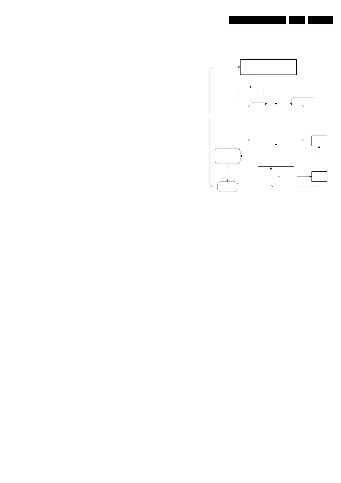
Figure 5-1 SDM Flowchart
How to enter SDM
Use one of the following methods:
• Use the standard RC-transmitter and key in the code
062596, directly followed by the MENU button.
• Short jumpers 1 and 2 of connector 0382 on the SCAVIO
panel.
After entering SDM, a blank screen is visible, with SDM in the
upper left side for recognition. The Blinking LED procedure is
started and will indicate any possible errors via the (orange)
front LED.
How to navigate
To toggle to the SAM mode, use a standard customer RCtransmitter and key in the code 062596, directly followed by the
OSD (i+) key.
How to exit
Use one of the following methods (the set returns to its last
status):
• Switch the set to STANDBY by pressing the power button
on the remote control transmitter (if you switch the set 'off'
by removing the Mains power, the set will return in SDM,
when the Mains power is re-applied).
• Use the standard RC-transmitter and key in the code 00.
5.2.2 Service Alignment Mode (SAM)
Purpose
• To perform (software) alignments.
• Easy way to identify the commercial type number of the
set.
• Easy identification of the used software versions.
• To display (or clear) the error code buffer.
• View operational hours.
Specifications
• Operation hours counter.
• Software version reading.
• Error buffer reading and erasing.
• Software alignments.
EN 14 FM242 AA5.
RC button,
e.g. P+ or P-
STANDBY
Do not store
settings made
during alignments
RC button,
e.g. P+ or P-
"UNDO" ignore
all "Service
unfriendly
modes"
"Standby"
Settings made
during alignments
are stored
STANDBY
NORMAL OPERATION
RC sequence "0-6-2-5-9-6-OSD "(for Europe & A/P)
RC sequence "0-6-2-5-9-6-INFO+" (for USA/LatAm)
Short SAM pins (works also from Standby)
RC sequence
"00"
or
or
Ignore all "Ser vice
unfriendly" mod es
Service Alignment Mode
Display "SAM" top level
menu
Upper menu selection
(with cursor buttons)
Lower menu selection
(with cursor buttons)
RC-code "0-6-2-5-9-6-OSD"
RC-code "0-6-2-5-9-6-INFO+"
RC-code "0-6-2-5-9-6-MENU" -
Service Modes, Error Codes and Fault Finding
Mains ON
OFF
(Settings made
during alignments
are stored)
Mains OFF
or
SAM submenus
(whitepoints, align-
ments, etc.)
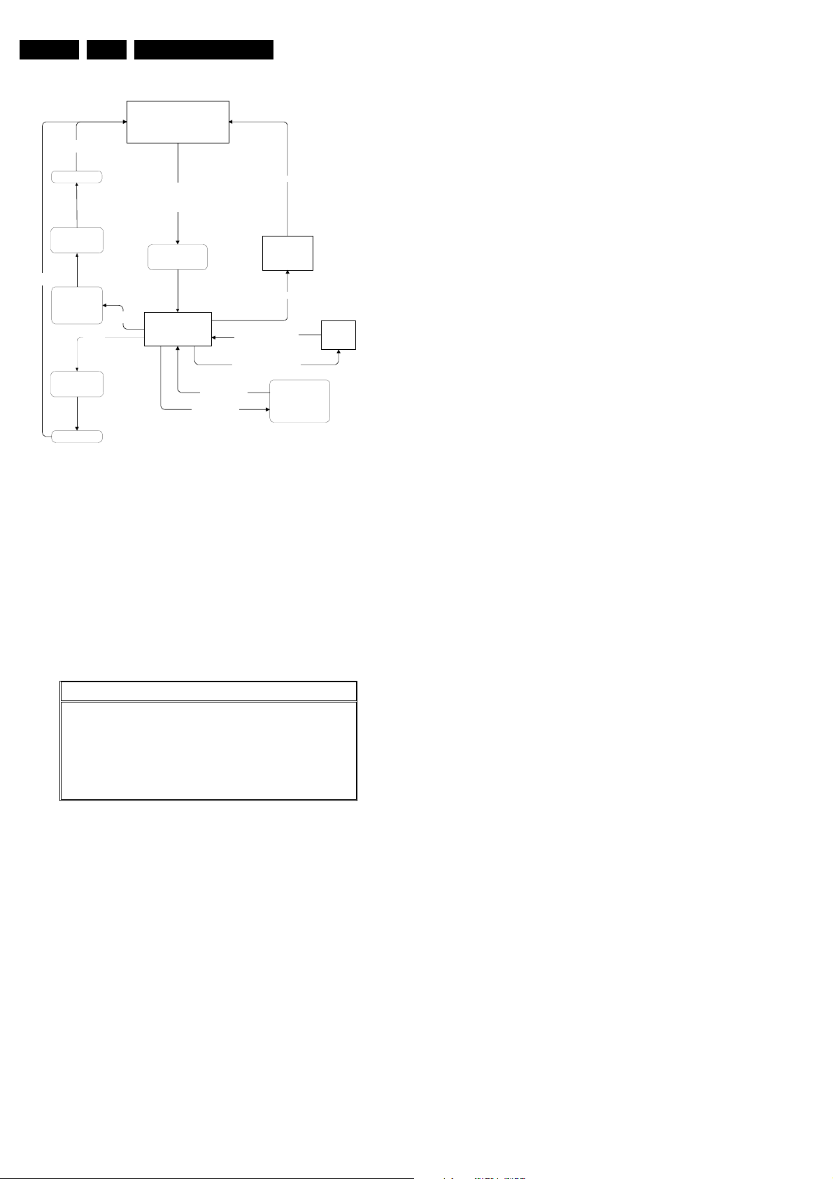
Figure 5-2 SAM Flowchart
How to enter
Use one of the following methods:
• Use a standard RC-transmitter and key in the code 062596
directly followed by the OSD (i+) button
Note: the OSD (i+) is not available on the original FM242
remote control, therefore use another Philips remote
control (e.g. MG, EMG or A10).
• Short jumpers 3 and 4 of connector 0382 on the SCAVIO
panel.
The following screen is visible:
Service Alignment Menu General
Type Nr. - AG Code 42FD9945/01 **00 00
SW Version OTC AAAAAB-X.Y_xxxxx
SW Version PW AAAABC-X.Y_xxxxx
SW Version EPLD AAAABC-X.Y_xxxxx
Errors 1 xx xx xx xx xx
Errors 2 xx xx xx xx xx
Operational hours xx
Reset error buffer Press OK to reset
Store Press OK to store
CL 26532011_016.eps
SDM
CL 16532099_101.pdf
260901
200303
4. SW Version PW (AAAABC-X.Y-xxxxx). See description
above.
5. SW Version EPLD (AAAABC-X.Y-xxxxx). See description
above.
6. Errors 1. Gives the last five errors of the error buffer. The
last detected error is displayed at the most left position.
The errors are displayed as 2 digit numbers and separated
by a space. When less than 10 errors occurred, the rest of
the line(s) is empty. In case of no errors the text 'No Errors'
is displayed behind menu item 'Errors 1'. See paragraph
5.5 for a description.
7. Errors 2. Gives the first five errors of the error buffer. The
last detected error is displayed at the most left position.
8. Operational hours. The Operations Hours indicate the
time that the display was active with half an hour resolution.
It represents the system hours (OTC), not the PDP hours.
9. Reset error buffer. Erase the contents of the error buffer.
Press 'OK' on your remote control to activate. The content
of the error buffer is cleared.
10. Store. This will store the performed alignments. Press 'OK'
on your remote control to activate.
Note: if you do not want to store the performed alignments,
leave the SAM mode via code 00 on your remote control.
Do not activate the 'store' item.
How to navigate
Use one of the following methods:
• Select the sub-menu's (upper line) with the CURSOR
LEFT/RIGHT keys on the remote control transmitter.
• Select the menu items with the CURSOR UP/DOWN keys.
With the CURSOR LEFT/RIGHT keys it is possible to:
– Activate the selected menu item.
– Change the value of the selected menu item.
• To toggle to the SDM mode, use the standard customer
RC-transmitter and key in the code 062596, directly
followed by the MENU key.
How to exit
Use one of the following methods:
• Switch the set 'off' (with the Mains switch or by pulling the
Mains cord).
Note: new alignment settings are always stored, even
when item 'store' was not activated!
• Switch the set to 'standby' by pressing the power button on
the remote control transmitter.
Note: new alignment settings are always stored, even
when item 'store' was not activated!
• Use the standard RC-transmitter and key in the code 0 0.
Note: new alignment settings are not stored (except when
item 'store' was activated)!
5.2.3 Customer Service Mode (CSM)
Figure 5-3 SAM Menu 'General'
1. Type Nr. Gives the commercial type number of the
monitor, e.g. 42FD9945/01.
2. AG Code. Is not implemented.
3. SW Version OTC (AAAAAB-X.Y-xxxxx).
Note: You will find details of the latest software versions in
the chapter 'Software Survey' of the 'Product Survey Colour Television' publication, which is published four
times each year.
• A = the chassis name (FM23 for 32" displays or FM242
for 42" SDI-displays).
• B = the region (E= Europe, A= Asia Pacific, U= NAFTA,
L= LATAM; in our case G = Global).
• (if valid) C = the configuration name (B= Basic, E=
Enhanced; for PW & EPLD-software this will be named
B).
• X = the main software version number.
• Y = the sub software version number.
• x = last five digits of 12nc code.
Purpose
When a customer is having problems with his TV-set, he can
call his dealer or helpdesk. The service technician can than ask
the customer to activate the CSM, in order to identify the status
of the set. Now, the service technician can judge the severe
ness of the complaint. In many cases, he can advise the
customer how to solve the problem, or he can decide if it is
necessary to visit the customer.
The CSM is a read only mode, therefore modifications in this
mode are not possible.
Service Modes, Error Codes and Fault Finding
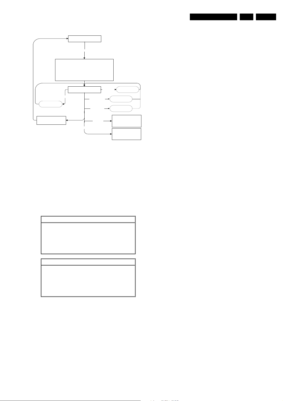
Normal operati on mode
Key in sequence: 1-2-3-6-5-4 on RC
Store current picture, sound and feature settings for later
retrieval (only store if needed to go back to normal
operation).
Set pre-defined picture, sound and feature settings (to be
able to see and hear if the set is working pr operly and to be
able to read the CSM information).
Ignore service unfriendly options
Volume up/down
Numerical key,
external
If other key
= standby
"Cursor right"
To previous CSM page
Restore picture, sound and
feature settings (that were
stored during entry)
Display CSM information screen
"Cursor left"
Other key,
e.g. "menu"
mains off
Figure 5-4 CSM Flowchart
How to enter
Use the standard customer RC-transmitter and key in the code
123654.
When CSM is entered, the values of brightness, contrast, etc.
are set to 50% (of max. value), and volume is set to 25%, to
ensure that you always have a picture and sound.
After switching 'on' the Customer Service Mode, the following
screen will appear:
Customer Service Menu 1
1 - Type Nr. - AG Code 42FD9945/01
2 - SW Version OTC AAAAAB-X.Y_xxxxx
3 - SW Version PW AAAABC-X.Y_xxxxx
4 - SW Version EPLD AAAABC-X.Y_xxxxx
5 - Code 1 xx xx xx xx xx
6 - Code 2 xx xx xx xx xx
7 - Volume xx
8 - Brightness xx
9 - Contrast xx
Customer Service Menu 2
10 - Colour xx
11 - Tint xx
12 - Sharpness xx
13 - Soundmode xx
14 - Source xx
15 - AV Mute xx
Figure 5-5 CSM Menu
To next CSM page
Increase/decrease
volume
Switch to prese t/
channel or external
Standby
(when the set is switched on,
picture, sound and feature
settings (that were stored
during entry) are restored)
Off
(when the set is switched on,
picture, sound and feature
settings (that were stored
during entry) are restored)
CL 16532099_103.pdf
CL 36532011_015.eps
200303
260901
EN 15FM242 AA 5.
• (if valid) C = the configuration name (B= Basic, E=
Enhanced).
• X = the main software version number.
• Y = the sub software version number.
• x = last five digits of 12nc code.
3. SW Version PW (AAAABC-X.Y-xxxxx). See description
above.
4. SW Version EPLD (AAAABC-X.Y-xxxxx). See description
above.
5. Code 1. Gives the last five errors of the error buffer. The
last detected error is displayed at the most left position.
The errors are displayed as 2 digit numbers and separated
by a space. When less than 10 errors occurred, the rest of
the line(s) is empty. In case of no errors, the text 'No Errors'
is displayed behind menu item 'Code 1'. See paragraph
“Error Buffer” for a description.
6. Code 2. Gives the first five errors of the error buffer. The
last detected error is displayed at the most left position.
7. Volume. Gives the last volume status for the selected
source, as set by the customer.
8. Brightness. Gives the last brightness status for the
selected source, as set by the customer.
9. Contrast. Gives the last contrast status for the selected
source, as set by the customer.
10. Colour (not present in Basic configuration). Gives the last
colour status for the selected source, as set by the
customer.
11. Tint (only for NTSC Enhanced configuration). Gives the
last tint status for the selected source, as set by the
customer.
12. Sharpness. Gives the last sharpness status for the
selected source, as set by the customer.
13. Source. Gives the selected source, as set by the
customer.
14. AV Mute. Indicates if AV Mute is 'on' or 'off'.
How to navigate
Use one of the following methods:
• Switch to the other CSM page with the CURSOR LEFT/
RIGHT keys on the remote control.
• You can increase/decrease volume with the VOLUME UP/
DOWN keys on the remote control.
• You can switch to another source with the NUM/EXT keys
on the remote control.
How to exit
Use one of the following methods:
• Press the MENU key of the remote control transmitter.
• Switch the set to 'standby' with the Power switch on the
remote control.
• Switch the set 'off' with the Mains power switch.
5.3 Problems and Solving Tips (Related to CSM)
5.3.1 Picture Problems
Note: Below described problems are all related to the monitor
settings. The procedures to change the value (or status) of the
different settings are described.
1. Type Nr. AG Code. Gives the commercial type number of
the monitor, e.g. 42FD9945/01. AG Code is not
implemented.
2. SW Version OTC (AAAAAB-X.Y-xxxxx) Note: You will find
details of the latest software versions in the chapter
'Software Survey' of the 'Product Survey - Colour
Television' publication, which is published four times each
year.
• A = the chassis name (FM23 for 32" displays or FM242
for 42" SDI-displays).
• B = the region (E= Europe, A= Asia Pacific, U= NAFTA,
L= LATAM or G = Global).
Picture too dark or too bright
Increase/decrease the BRIGHTNESS and/or the CONTRAST
value when the picture improves after you have switched on
the Customer Service Mode. The new value is automatically
stored.
White line around picture elements and text
Decrease the SHARPNESS value when the picture improves
after you have switched on the Customer Service Mode. The
new value is automatically stored.
Snowy picture and/or unstable picture
A scrambled or decoded signal is received.

EN 16 FM242 AA5.
Service Modes, Error Codes and Fault Finding
Black and white picture
Increase the COLOUR value when the picture improves after
you have switched on the Customer Service Mode. The new
value is automatically stored.
Menu text not sharp enough
Decrease the CONTRAST value when the picture improves
after you have switched on the Customer Service Mode. The
new value is automatically stored.
5.3.2 Sound Problems
(if valid, related to speaker-version yes or no)
No sound from left or right speaker
Check item 'Volume' in the CSM mode. If value is low, increase
the volume level. The new value is automatically stored.
No sound or sound too loud (after channel change/ switching on)
Increase/decrease the VOLUME level when the volume is OK
after you switched on the CSM. The new value is automatically
stored.
5.4 ComPair
5.4.1 Introduction
ComPair (Computer Aided Repair) is a service tool for Philips
Consumer Electronics products. ComPair is a further
development on the European DST (Dealer Service Tool),
which allows faster and more accurate diagnostics. ComPair
has three big advantages:
• ComPair helps you to quickly get an understanding on how
to repair the chassis in a short time by guiding you
systematically through the repair procedures.
• ComPair allows very detailed diagnostics (on I
is therefore capable of accurately indicating problem areas.
You do not have to know anything about I
yourself because ComPair takes care of this.
• ComPair speeds up the repair time since it can
automatically communicate with the chassis (when the
microprocessor is working) and all repair information is
directly available. When ComPair is installed together with
the SearchMan electronic manual of the defective chassis,
schematics and PWBs are only a mouse click away.
5.4.2 Specifications
ComPair consists of a Windows based faultfinding program,
and an RS232 cable between PC and the (defective) product.
The ComPair faultfinding program is able to determine the
problem of the defective monitor. ComPair can gather
diagnostic information in two ways:
• Automatic (by communication with the monitor): ComPair
can automatically read out the contents of the entire error
buffer. Diagnosis is done on I2C level. ComPair can send
and receive commands to the micro controller of the
monitor, and so can access the I2C bus of the monitor. In
this way, it is possible for ComPair to communicate (read
and write) to devices on the I2C busses of the FTV monitor.
• Manually (by asking questions to you): Automatic
diagnosis is only possible if the micro controller of the
monitor is working correctly and only to a certain extend.
When this is not the case, ComPair will guide you through
the faultfinding tree by asking you questions (e.g. Does the
screen give a picture? Click on the correct answer: YES /
NO) and showing you examples (e.g. Measure test-point
F7 and click on the correct oscillogram you see on the
oscilloscope). You can answer by clicking on a link (e.g.
2
C level) and
2
C commands
text or a waveform picture) that will bring you to the next
step in the faultfinding process.
By a combination of automatic diagnostics and an interactive
question / answer procedure, ComPair will enable you to find
most problems in a fast and effective way.
Beside fault finding, ComPair provides some additional
features like:
• Software upgrading (upload possible to OTC and PW
Scaler).
• Emulation of the (European) Dealer Service Tool (DST).
• If both ComPair and SearchMan (Electronic Service
Manual) are installed, all the schematics and the PWBs of
the set are available by clicking on the appropriate
hyperlink. Example: Measure the DC-voltage on capacitor
C2228 (Schematic/Panel) of the SCAVIO panel. Click on
the 'Panel' hyperlink to automatically show the PWB with a
highlighted capacitor C2568. Click on the 'Schematic'
hyperlink to automatically show the position of the
highlighted capacitor.
5.4.3 How to Connect
1. First, install the ComPair Browser software on your PC
(read the installation instructions carefully).
2. Connect an RS232 interface cable between a free serial
(COM) port on your PC and the RS232 connector on the
FM242 plasma monitor.
3. Switch the plasma monitor 'off' and 'on' again (with the
Mains switch).
4. Start the ComPair program and follow the instructions.
Note: once the set is in ComPair mode, the front LED will blink
red, at a frequency of 0.3 Hz.
5.4.4 How to Order
ComPair order codes:
• Starter kit ComPair32 software (registration version): 3122
785 60040.
• ComPair32 CD (update): 3122 785 60070.
• Starter kit SearchMan32 software: 3122 785 60050.
• SearchMan32 CD (update): 3122 785 60080.
Note: The RS232 cable is not included. It is a standard cable
(9p sub-D male-to-female) that can be obtained by a computer
store. It is supplied however with the ComPair interface (4822
727 21631), necessary for servicing other Philips TVs.
5.5 Error Buffer
The error code buffer contains all detected errors since the last
time the buffer was erased. The buffer is written from left to
right. When an error occurs that is not yet in the error code
buffer, it is written at the left side and all other errors shift one
position to the right.
5.5.1 How to Read the Error Buffer
Use one of the following methods:
• On screen via the SAM (only if you have a picture).
Examples:
–Errors: 6 0 0 0 0, error code 6 is the last and only
detected error.
–Errors: 9 6 0 0 0, error code 6 was first detected and
error code 9 is the last detected (newest) error.
• Via the blinking LED procedure (when you have no
picture). See paragraph “The blinking led procedure”.
•Via ComPair.
Service Modes, Error Codes and Fault Finding
EN 17FM242 AA 5.
5.5.2 How to Clear the Error Buffer
The error code buffer is cleared in the following cases:
• By activation of the 'Reset error buffer' command in the
SAM menu.
• When you transmit the code 062599 with a standard
remote control transmitter.
5.5.3 Error Codes
Table 5-1 Error code overview
Error Device Description Item Diagr.
1 TEA6422D Audio switch
2 MSP3451G Sound proces-
3 PCF8574-
SCAVIO
4 PCF8591 AD-DA expand-er7530 SC8
5 FS6377 Clock generator 7570 SC9
6 PCF8574-PSU I/O expander
7 24C16 OTC NVM OTC 7430 SC7
8 24C16 PW NVM PW 7580 SC9
9 SAA7118 Video decoder
10 AD9887 ADC/TMDS re-
11 SDA9400 De-interlacer
12 EP1K30QC EPLD processor 7656 SC11
13 PDP I2C error of the
20 Download comm. Errors during
21 CSP comm. CSP time-out er-
40 Temperature alarm Detections of
70 Over voltage Vs, Va, +5V,
71 Vs under voltage Vs under voltage Black
72 Va under voltage Va under voltage Black
73 +5V under voltage +5V under volt-
74 +3V3 under voltage +3V3 under volt-
75 DC-PROT Audio amplifier
Notes:
• In case of non-intermittent faults, clear the error buffer
before you begin the repair. This to ensure that old error
codes are no longer present.
• If possible, check the entire contents of the error buffer. In
some situations, an error code is only the result of another
error code and not the actual cause (e.g., a fault in the
protection detection circuitry can also lead to a protection).
• In case error 70 occurs, the belonging over-voltage line
cause can be located via measuring. (via measuring all 4
voltages simultaneously with an oscilloscope). Chosen
(only Enhanced)
sor
I/O expander
SCAVIO
PSU
(only Enhanced)
ceiver
(only Enhanced)
PDP
downloading
ror
over-temperature
+3V3 overvoltage
age
age
protection
7798 SC13
7812 SC14
7540 SC8
7370 P3
7225 SC5
7170 SC4
7280 SC5
Black
P
box
P
box
P
box
Black
P
box
Black
P
box
Black
P
box
FM242-workshops will be trained how to do so. (special
document will be generated for this).
5.6 The Blinking LED Procedure
Via this procedure, you can make the contents of the error
buffer visible via the front LED (orange colour).This is
especially useful when there is no picture. When no errors are
present, the LED will stay green.
When the SDM is entered, or when code 062500 is entered
with the remote control, the LED will blink the contents of the
error-buffer.
Error-codes ≥ 10 are shown as follows:
1. n long blinks of 750 ms, which is/are an indication of the
decimal digit,
2. a pause of 1.5 s,
3. n short blinks (n = 1-9),
4. when all the error-codes are displayed, the sequence
finishes with a LED blink of 3 s,
5. the sequence starts again.
Example of error buffer: 12 9 6 0 0
After entering SDM:
1. 1 long blink of 750 ms followed by a pause of 1.5 s,
2. 2 short blinks followed by a pause of 3 s,
3. 9 short blinks followed by a pause of 3 s,
4. 6 short blinks followed by a pause of 3 s,
5. 1 long blink of 3 s to finish the sequence,
6. the sequence starts again.
5.7 Protections
You can read the error codes of the error buffer via the service
menu (SAM), the blinking LED procedure, or via ComPair. If a
fault situation is detected an error code will be generated and if
necessary, the set will be put in the protection mode. Blinking
of the red LED at a frequency of 5 Hz indicates the protection
mode.
In some error cases, the microprocessor does not put the set
in the protection mode. The error codes are indicated by an
orange front LED.
To get a quick diagnosis the chassis has three service modes
implemented:
• The Customer Service Mode (CSM): easy way to read out
the status of the set.
• The Service Default Mode (SDM): start-up of the set in a
predefined way.
• The Service Alignment Mode (SAM): adjustment of the set
via a menu and with the help of test patterns.
Exceptional ‘protection’ situation
There exists one ‘protection’ (due to too high internal settemperature), where the set does not switch to ‘protection’mode but to Standby-mode. This protection is not logged into
the error-buffer.
When the set becomes too warm, an ‘On Screen Display’message will be showed set is going to switch to Standby. After
some time set can be switched on again. (It is very unlikely this
will happen. For that reason this performance has been
accepted).
Temperature error
The monitor will switch to standby
automatically.
Please allow cool down.

EN 18 FM242 AA5.
5.8 Repair Tips
If one of the errors of the error buffer points to a defective
supply, then the supply-panel must be send for central repair.
If the symptoms (still to be communicated; e.g. when VS-value
is too high some pixels do not extinguish, when VS-value is too
low some pixels do not enlighten) match with a possible
misalignment of a supply-line, this supply-line could be
checked, and re-aligned.
Only do this if there is a slight spec-violation.
In case it does not help, re-align to the previous wrong setting,
to keep cause-image in tact, for central repair workshop.
Replace supply panel by a new one, and match the supply with
the pdp. (See alignment instructions in chapter “Alignments”).
Service Modes, Error Codes and Fault Finding
Block Diagrams, Testpoint Overviews, and Wiring Diagram
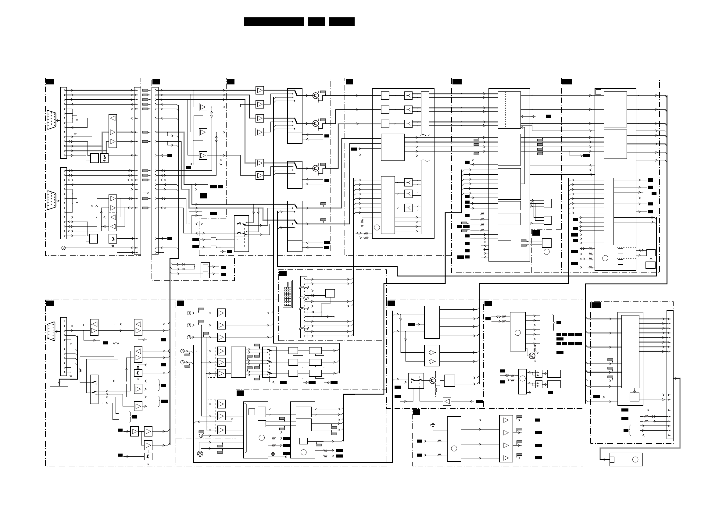
6. Block Diagrams, Testpoint Overviews, and Wiring Diagram
Block Diagram Video
VIDEO
VGA
VGA
CONNECTOR
0371 0318 0318
VGA1-R
1
VGA1-G
2
VGA1-B
3
VGA1-TXD
4
VGA1 IN
15P"D"SHELL
CONNECTOR
5
6
6
1
11
7
2
12
7
8
3
13
9
8
4
14
10
15
VGA2
IN/OUT
15P"D"SHELL
CONNECTOR
6
11
7
12
8
13
9
14
10
15
RC-OUT
SC6
RS-232
IN/OUT
5
10
4
9
3
8
2
7
1
6
BLOCK DIAGRAM
5
1
2
3
4
5
RS 232 INPUT
CONTROL
RC-VGA1
9
10
VGA1-RXD
11
DCC-SDA-1
12
VGA1-H
13
VGA1-V
14
DCC-SCL-1
ST24FC21
VGA2-R
VGA2-G
VGA2-B
VGA2-TXD
VGA2-RXD
DDC-SDA-2
VGA2-H
VGA2-V
DDC-SCL-2
RXD
TXD
5
DDC
7
NVM
7904
DDC
NVM
7907
ST24FC21
+5V-STBY-SW +5V-STBY-SW
7352
ST3232E
11
14
12
13
6366
PS-232-ACT
SC7
3913
7340 A+B
74HC4052D
1
TXD-OTC
3
5
TXD-PW
12
13
14
10
9
LOGIC
6
15
0372
1
2
3
4
5
6
7
8
9
N.C.
10
11
12
13
14
15
0376
1
2
3
RL_ICN
4
5
GL_ICN
6
LD_ICN
7
IR_TX
8
IR_RX
9
10
11
SEE
6
1
13
9
2
11
6
7900
EBOX-PRESENT
10
7937
7940
7910
VGA1-R
VGA1-G
VGA1-B
VGA1-TXD
VGA1-RXD
9
RC-VGA1
4
VGA1-H
10
VGA1-V
VGA2-R
VGA2-G
VGA2-B
VGA2-TXD
VGA2-RXD
8
VGA2-H
VGA2-V
3
12
5
VGA-OUTN
7915
SELECT-3
SELECT-2
SC8
SC7
TXD-2
RXD-2
RC
RC-CONTR
11
9
10,13
3
5
7310
SC8
2
4
6
12
13
15
8
10
29
17
19
21
27
28
23
25
31
30
32
7303 C+D
7303 A+B
1.4
7315, 7316
7325, 7326
SC6
F303
31
F304
29
F305
27
F308
21
F309
20
18
F306
25
F307
23
4
F311
16
F312
14
F313
12
6
5
F314
10
F315
8
2
3
1
12
VGA2-TXD
8
VGA2-RXD
SELECT-4
26VGA1-RXD
VGA1-TXD
SELECT-1
VGA1-RXD
TXD-OTC
RXD-OTC
TDX-PW
RXD-PW
73237322
RC-OUT
7320
RC-VGA1
7321
VGA
INPUT
SC8
SC8
SC7
SC10
VGA1-R
VGA1-G
VGA1-B
VGA1-TXD
VGA1-RXD
RC-VGA1
VGA1-H
VGA1-V
(EBOX-
PRESENT)
SC7
TV MODE
VGA2-TXD
VGA2-RXD
VGA2-H
VGA2-V
VGA2OUTN
SC6
RC-OUT
6379
6378
SC3
R/Pr/Cr
G/Y/Y
B/Pb/Cb
2fh 1fh 2fh
V
H
VGA2OUTN
SC6
SC10
SC10
VGA1-V
VGA1-H
VGA1-RXD
VIDEO SELECTION
& MATRIX
AV3 (HD)
V-HD-EXT
F072
H-HD-EXT
F075
AV1
7311-A
7311-B
7311-C
VGA1-H
VGA1-V
11
F071
F070
Y-H D
F073
251
SVHS
SC2
VGA1-V
VGA1-H
VGA2-V
VGA2-H
VGA2-V
VGA2-H
VGA2-EN
VGA2-OUT
7370 A+B
O.S.
O.S.
F074
AV2
34
SC11
SYNC
SELECTION
SC11
7060
7065
75
9
R
G
B
Pr
Y
Pb
1Fh
Cr
Y
Cb
CVBS
C
Y
SC3
VGA2-R
VGA2-G
VGA2-B
SC7
VGA2-EN NOT
VGA2-OUTN
SC6
SYNC-ACT
SC7
UART-ACT
SC7
7141
7138
7135
70792Fh
7074
7084
1fh BUFFER
7117
Cr
7113
Ys
7121 Y-HD
Cb
F236
F235
VIDEO SELECTION
7007 A+C
74HCT4053T
14
4
6
11-9
7088
7090
MATRIX
LOGIC
RGB
SC5
MATRIX-SEL
8x
8x
H-DEC
V-DEC
clock
PW-SDA
3250
3250
PW-SCL
VGA1-R
VGA2-R
R-2Fh
R-YUV
VGA1-G
VGA2-G
G-2Fh
G-YUV
VGA1-B
VGA2-B
B-2Fh
B-YUV
VGA1-V
VGA2-V
VGA1-H
VGA2-H
SC4
4
15
14
Y-D E C
UV-DEC
F240
F247
1250
VIDCLK
24.576MHz
SC11
V-HD
12,14
H-HD
1,5
SC10
2
4
1
5
15
11
12
14
2
4
1
5
2
4
15
11
SC9
SC9
7146
74HC4052D
LOGIC
7158
74HC4052D
LOGIC
7009
74HC4052D
LOGIC
DVI-D INPUT
DVI-D INPUT SOCKET
7102
CLAMP
7103
CLAMP
7104
CLAMP
7280
SDA 9400
23
22
54
0375
INTERLACER
CLOCK
7145
7148
7151
7154
7157
7160
12
13
5
3
R-2Fh
G-2Fh
B-2Fh
7089
I054
74HCT4053D
R-NTSC
R-ATSC53
I058
I065
G-NTSC
G-ATSC21
I072
I078
B-NTSC
B-ATSC123
I083
VIDE-SELECTION
DECODER
DECODER DE-INTERLACER
7225
SAA7118C
VIDEO
DE-
ADC
CODER
SYNC
CNTRL
P4
ERR
9
10
14
16
17
18
23
24
SYNC
7129
F146
3
7130
F152
13
9
VIDEO-SEL-1
VIDEO-SEL-2
7131
VIDEO-SEL-1
VIDEO-SEL-2
V-ADC
H-ADC
SYNC-SEL
VIDEO-SEL-2
7100-B
BLANKING
7100-C
BLANKING
7100-A
BLANKING
SC11
HD-CLAMPN
SC8
F158
SC8
F211
F210
SC10
SC8
SCL
DDC
SDA65
EPROM
6210
R-YUV
G-YUV
B-YUV
8x8xY-OUT
UV-OUT
61
V OUT-DEINT
60 H OUT-DEINT
V PEN
62
CLKOUT-DEINT
26
F249
PW-SDA
3284
21
3285
20
PW-SCL
10
3
9
10
3
13
9
10
1
2
6
7
9
DE-
ERR
11
19FM242 AA 6.
SC11
HD-BLANKN
F246
F245
SC10
SC10
SC4
RX2-
RX2+
7215
ST24FC21
RX1-
RX1+
+5V-STBY-SW
RXD-
RXD+
RXC+
RXC-
VIDEO SELECTION - ADC
119R-ADC
110G-ADC
100B-ADC
GBLKSPL
SC10
GCOAST
RXO+
RXO-
RX1+
RX1-
RX2+
RX2-
RXC+
RXC-
PW-SDA
3209
PW-SCL
3210
7170
AD9887KS
81V-ADC
82H-ADC
93
94
62
63
59
60
56
57
65
66
53RTHERM DATACK
ERR
92
91
ADC-TMDS PW EPLD
8x
ADC
8x
ADC
8x
ADC
SYNC. PROC
+
CLOCK
GENERATION
8x
8x
TMDS
RECEIVER
8x
DE
SC2
H-SYNC
V-SYNC
SYNC SELECTION
& SWITCHING
Y-H D
C-SYNC-OUT
SC11
SC11
H-PRESNT
10
H-HD-EXT
2
1
8x
8x
8x
8x
8x
8x
8x
8x
8x
8x
8x
8x
V-HD-EXT
75 OHM-ON
SC11
7007-B
74HCT4053D
10 6
SC9
MUXES
7000 - 7002
7006 - 7010
PROCESSING
7025 A-B
LM319D
COMPARATOR
10
5
15
VGA2-EN-NOT
SCALER - CLOCK
GENERATOR
24.576 MHz
SC7
SC7
V-SYNC
H-SYNC
+
-
+
-
SDA-1
SCL-1
SCALER-PW164-MEMORY
SC10
8x GRE (0-7)
8x GRO (0-7)
8x GGE (0-7)
8x GGO (0-7)
8x GBE (0-7)
8x GBO (0-7)
138
139
140
134
137
7
12
+5B
7040
LM 1881M
2
3051
7060
3571
3570
16
SYNC
SLICER
7570
FS6377
5
6
GENERATOR
1
CLOCK
ERR
SC5
SC11
V-SYNC-TTL
V-SYNC-POL-N
H-SYNC-TTL
H-SYNC-POL-N
V-SYNC-CMP
H-SYNC-CMP
C-SYNC-LM
1
V-SYNC-LM
3
VGA2-EN
5
ADVS
ADHS
ADSOG
GCLK
ADDE
F615
F616
15
13
12
10
SC11
SC4
SC7
SC7
SC9
SC7
SC6
SC2
SC8
SC3
F619
F633
F618
CLKOUT-DEINT
8x UV-OUT
VOUT-DEINT
HOUT-DEINT
PW-START
PW-PRESET
SDA-2
SCL-2
PW-SDA
PW-SCL
RXD-PW
TXD-PW
VGA2-OUT
VGA2-EN
VIDEO-SEL-1
VIDEO-SEL-2
SYNC-SEL
SC10
GBLKSPL
GCOAST
8x Y-OUT
VPEN
MCLK
3608
3606
3604
3605
7605
PW164
CONTROL FUNCTIONS
SC8
SDA1
SC7
SCL1
SC7
SDA1
SCL1
SC7
7574
74LVC125A
5
9
GRAPHICS PORT
SYNC
DECODER
AND
TIMER
YUV
TO
RGB
CLOCK
GEN
MICRO-
PROCESSOR
UART
3541
15
14
3540
PIXEL PROC.
VIDEO
PORT
7540
PCF8574A
3532
3531
32
6
8
1112
8x DRE (0-7)
8x DGE (0-7)
SCALER
SC9
DCK EXT
8x DBG (0-7)
PARITY PARITY-OUT
F637
F639
F634
F638
7630
M29W160DT
DATA
FLASH
ADD
ROM
CNTRL
7628
CY62126
DATA
ADD
SRAM
CNTRL
PW-NVM
SC9
7580
M24C32
SDA
EXP.
ERR
10
I/O
3
9
F566
F565
F563
F564
F569
F567
7530
PCF8591
ADC
ERR
4
5
6
7
9
10
11
12
7563
1
4
2
3
VIDCLK
(24.567 MHz)
VXCA
(18.432 MHz)
MCLK
(120 MHz)
DCKEXT
(36 MHz)
5
SCL
6
SELECT-1
SELECT-2
SELECT-3
SELECT-4
VIDEO-SEL-1
POWER-DOWN
VIDEO-SEL-2
3548
MSP-RESET
0315
1
2
0316
1
2
TEMP3-SENSOR
SC5
SC14
AUDIO
SC10
SC10
NVM
ERR
8
TEMPSENSOR S1
(OPTIONAL)
TEMPSENSOR S2
(OPTIONAL)
P3
SC6
SC6
SC12
SC6 SC3
SC14
SC11
SC3
BACK-END-EPLD
DVS
DHS
DEN
DCLK
FBX MODE
1-2 FH
SYNC
SC5
SC6
SC10
SC8
SC10
SC12
SC10 SC11
SC10 SC11
SC12
V-SYNC-TTL
V-SYNC-POL-N
H-SYNC-TTL
H-SYNC-POL
C-SYNC-LM
V-SYNC-LM
V-SYNC-COMP
H-SYNC-COMP
VGA1-V
VGA1-H
VGA2-V
VGA2-H
SYNC-SEL
VIDEO-SEL-1
VIDEO-SEL-2
PW-SDA
PW-SCL
SDA-1-3V3
3664
SCL-1-3V3
3662
7656-A+B+C
EP1K30FC256
A
SC12
8x R-OUT (0-7)
8x G-OUT (0-7)
8x B-OUT (0-7)
V-SYNC-OUT
H-SYNC-OUT
BLANK-OUT
PARITY-OUT
SC10
PWDWN--LVDS
DIGITAL
CONTRAST
SYNC
DELAY
SYNC
PROC.
ERR
12
BACK-END-LVDS OUTP
7670
DS90CC385M
50-56
2-4
6-8
10-15
16,18-20
22-25
F619
28
F690
27
F692
30
25
DCLK
31
32
B
CONTROLS
C
SUPPLY
& GROUND
SC12
SC12
PLASMA
DISPLAY
PANEL
LVDS
TTL PARALLEL
TO
LVDS
(LVDS
ENCODER)
TTL
LVD S
POWER DOWN
SDA-1-3V3
SCL-1-3V3
PDP-GO
SC7
CPU-GO
IRQ-PDP
PDP
8x R-OUT (0-7)
8x G-OUT (0-7)
8x B-OUT (0-7)
V-SYNC-OUT
H-SYNC-OUT
BLANK-OUT
PWRDWN-LVDS
75 OHM-ON
SC2
H-PRESENT
SC2
HD_BLANKN
HD_CLAMPN
C-SYNC-OUT
SC2
TV MODE
SC6
V-HD
H-HD
7655
EPC2
DATA
CNTRL
PROM
585
PROG
SOCKET
48
TX OUT0-M
47
TX OUT0-P
46
TX OUT1-M
45
TX OUT1-P
42
TX OUT2-M
41
TX OUT2-P
38
TX OUT3-M
37
TX OUT3-P
3837TX CLK OUT-M
TX CLK OUT-P
3680
3684
ERR
30
CL 26532038_001.eps
SC3
PDP
INTERFACE
CONNECTOR
PDP-GO
CPU-GO
IRQ-PDP
0318
19
17
15
13
11
9
3
1
7
5
4
14
18
8
10
6
150402

Block Diagrams, Testpoint Overviews, and Wiring Diagram
Block Diagram Audio
20FM242 AA 6.
AUDIO
AUDIO SOURCE
SC13
SELECT
L
AUDIO
VGA IN
R
L
AUDIO
FLEX
VGA
R
L
AUDIO
DVI-D
R
L
AV1
AUDIO
CVBS
R
L
AV2
AUDIO
YC
R
AV3
L
AUDIO
RGB
YPbPr
R
YCbPr
SC1-L
SC1-R
D-CTR-NIL
D-CTR-ONE
CONTROL
LED
LD
PANEL
7107
RC
RECEIVER
2
6127
1101
4
ON/OFF
5
SWITCH
6
7120
F713
F714
1
4
SC8
SC6
GREEN
RED
F710
F711
RS-232
IN/OUT
2
6
2
A
6
B
2
6
7800 A+B
74HC4053D
2
12
7718
POWER-OK
RS232 INPUT
5
10
4
9
3
8
2
7
1
6
6103
2
3
7
1
2
3
7714
LM833D
7734
LM833D
7754
LM833D
0376
1
2
3
4
5
6
7
8
9
10
11
10,11
7103
7105
1
7
1
7
1
7
15
14
ANTI PLOP
+9V-STBY
7801
7802
BLOCK DIAGRAM
RXD
TXD
RL_ICN
GL_ICN
LD_ICN
IR_TX
IR_RX
GREEN-LED
RED-LED
RC-IN
LIGHT-SENSOR-IN
+8V6
+5V-STBY-SW
+9V-STBY-SW
+9V-STBY
L4
R4
L5
R5
L6
R6
L2
R2
L3
R3
L1
R1
7803
SEE
VIDEO
N.C.
L1
L2
L3
L4
L5
L6
R1
R2
R3
R4
R5
R6
7805
7806
AUDIO-ENABLE
SC14
0320
1
2
3
4
5
6
7
8
9
10
5798
+8V6
SC8
0320
1
2
3
4
5
6
7
8
9
10
10
11
25
24
23
20
19
18
7798
TEA6422D
3
ERR
4
5
6
9
MATRIX
SWITCH
7807
7808
CONTROL
FUNCTIONS 2
ICON_NOT
ICON_NOT
1
LD_ICN
GL_ICN
RL_ICN
SC7
IR_TX
IR_RX
SC7
+8V6
+5V-STBY-SW
+9V-STBY-SW
+9V-STBY
SC14
3795
28 SDA-AUDIO
3794
27
12 PRE-OUT1-L
13
PRE-OUT1-R
SC15
AUDIO
DELAY LINE
A
B
7555
74HC4053D
2
1
12
13
5
3
7550
74HC4053D
2
1
12
13
AUDIO-PROCESSOR
SCL-AUDIO
GREEN_LED
15
14
RED_LED
4
15
14
BLOCK DIAGRAM
RC
VIDEO
I2SDATA-IN1
I2SDATA-IN2
B
7879
TC74HC590AF
RC
SC6
SEE
7812
MSP3415G
3
2
17
21
40
41
DEMO-
DULATOR
PRE-
SCALE
DAC
DIGITAL
DAC
SOUND
7874
TC74HC590AF
F872
CONTROL FUNCTIONS 1
SC7
SC6
SC6
7517
ADM 810
RESET
DSP
PROC.
VGA1-H
VGA1-V
2
ERR
2
I2S-DATA-OUT
I2S-CLOCK
DACM-L
DAC
DACM-R
DAC
7870
TC74HC590AF
7432
7433
RESET
SC13
SERVICE PINS
0382
1
3
5
7
9
+5V
SDA-AUDIO
SCL-AUDIO
13
12
16
14
27
26
8
9
3130L
R
5 18.432 MHz VXCA
6
7x
7x
1415
6MHz
OTC-H
RESET
SC7
SC10
PW_FLASH_RESET
ICONN_NOT
SC8
STANDBY
SC8
SC10
PW-START
SC8
POWER-OK
CPU-GO
PDP-GO
SC12
IRQ-PDP
SC6 RC-CNTL
SC10
PW-RESET
SC10
PW-START
SC8 FAN-SP2
SC8 FAN-SP1
SC6 UART-ACT
SC6
SYNC-ACT
GND-LED
RED-LED
RC
LIGHT-SEN-IN
2
SDM
4SAM
6CMP
8
10
3813
3812
4810
4811
A
B
I660
I659
7841
LM833D
3
6
7851
LM833D
3
6
7861
TS462CD
2
6
SC9
SDA-1
SCL-1
1
7
F813
1
7
1
7
AUDIO DELAY PROC.
A
7880
CY7C199B
RAMCOUNTER COUNTER "D" F.F. "D" F.F.
SERVICE-IN
3419
3380-C
3422
3421
SCL-1
SDA-1
16
17
83
84OTC-V
74
109
120
119
95
96
116
115
93
110
108
95
104
103
99
98
114
113
100
105
106
SC7
7x8x
7383
SAA5801H
7881
74HCT573
8x
FRAME
OTC
ERR
91
ERR
92
ERR
93
ERR
94
ERR
95
ERR
96
ERR
97
8x
82
86
85
88
87
89
90
91
92
43
42
40
41
SC13
F816
SC7
F817
3404-C
3404-D
3404-A
3404-B
3402-D
3402-C
3402-B
3402-A
3464-D
3464-C
3464-A
3464-B
L-POS
L-NEG
AUDIO-ENABLE
D-CTR-ONE
D-CTR-NIL
7882
74HCT573
SDA-NVM-1
SCL-NVM-1
RESET
SC7
ROM-CS
RAM-CS
ROM-OE
RAM-OE
DATA
ADDRESS
CONTROL
DATA
ADDRESS
CONTROL
SC6
RS_232_ACT
F812
SC1-L
SC1-R
17
15
F383
F427
SDA-1
F428
SCL-1
F425
SDA-2
F426
SCL-2
RXD-OTC
TXD-OTC
R-POS
R-NEG
10
0388
7
6
5
4
3
2
1
4884
24 ms MONITOR
4894
40 ms TV
SEE
IIC DIAGRAM
SC10
SC6
7430
MC24C32
5
6
NVM
ERR
7
7
7510 - 74 LVCOOAD
1
2
9
7506
AM29DL164DT
DUAL
BANK
FLASH
ROM
7500
MSM51V18165F
DRAM
7435
A2
0388
88
7
6
5
4
3
2
1
FILTERS
+9V-STBY A
I2S-DATA-IN1
I2S-DATA-IN2
6
11
26
28
7515,7516
12
L-POS
L-NEG
AUDIO-ENABLE
R-POS
L-NEG
CS
OE
CS
OE
FLASH
RESET
7225
LM833DT
3
2
5
6
3207
3222
7211
BC857BM
AUDIO
A3
AMPL-
1730
2.5A
7735,7736
STAB
1740
2.5A
7745,7746
STAB
A4
A5
A6
7302
7402
7502
7602
L-HIGH
AUDIO
AMPLL-LOW
AUDIO
AMPLR-HIGH
AUDIO
AMPLR-LOW
F730
F735
F740
F745
7315
LM311D
2
3
7415
LM311D
2
3
7515
LM311D
2
3
7615
LM311D
2
3
A3
A4
A5
A6
7260-A
LM833DT
3
1
2
3259
F231
3220
1
7238-A
LM833DT
F241
3240
7
F211
TO
0302
P6
POWER
SUPPLY
3
1
2
3234
7260-B
LM833DT
5
7
6
3274
7238-B
LM833DT
5
7
6
3244
SUPPLY & DC PROTECTION
A7
0302
9
8
7
6
5
4
3
2
1
L-HIGH
L-LOW
AU-EN-NOT
R-HIGH
L-HIGH
DC-PROT
+9V-STBY
F258
F235
F273
F245
8
1,4
8
1,4
8
1,4
8
1,4
OUT_PROT
VSDN-POS
VCC-10-POS
VSDN-NEG
VCC-10 -NEG
7
7
7
7
3315
3328
F328
3318
3415
3428
F428
3418
3515
3528
F528
3518
3615
3628
F628
3618
OUT_LH
OUT_LL
OUT_RH
OUT_RL
VCC-10-POS
VCC-10-NEG
VCC-10-POS
VCC-10-NEG
VCC-10-POS
VCC-10-NEG
VCC-10-POS
VCC-10-NEG
VCC_10_POS
3749
VCC_10_NEG
F330
F430
F530
F630
3755
3765
2760
3330
7330
2330
2355
7355
3355
3430
7430
2430
2455
7455
3455
3530
7530
2530
2555
7555
3555
3630
7630
2630
2655
7655
3655
3770 3771 3780
+9V-STBY
+9V-STBY A
6750
2759
6760
7755
3337
3362
3437
3462
3537
3552
3637
3662
7751
7365-2
IRF7343
G
F365
G
7365-1
IRF7343
7465-2
IRF7343
G
F465
G
7465-1
IRF7343
7565-2
IRF7343
G
F565
G
7565-1
IRF7343
7665-2
IRF7345
G
F665
G
7665-1
IRF7345
5753
3751
7761
DC-PROT
5335
D
S
D
S
7340
D
S
D
S
7440
D
S
D
S
7540
D
S
D
S
7640
3781
CL 26532038_002.eps
VSDN-POS
5365
2355
5366
VSDN-NEG
OUT_PROT
A7
5435
VSDN-POS
5465
2465
5460
VSDN-NEG
OUT_PROT
A7
5535
VSDN-POS
5565
2565
5560
VSDN-NEG
OUT_PROT
A7
5335
VSDN-POS
5665
2665
5660
VSDN-NEG
OUT_PROT
A7
DC-PROTECT
7753
BC857BW
3752
150402
OUT_LH
OUT_LL
OUT_RH
OUT_RL
0303
0304
5
L-HIGH
4
3
2
1
L-LOW
R-HIGH
4
3
2
1
R-LOW
Block Diagrams, Testpoint Overviews, and Wiring Diagram
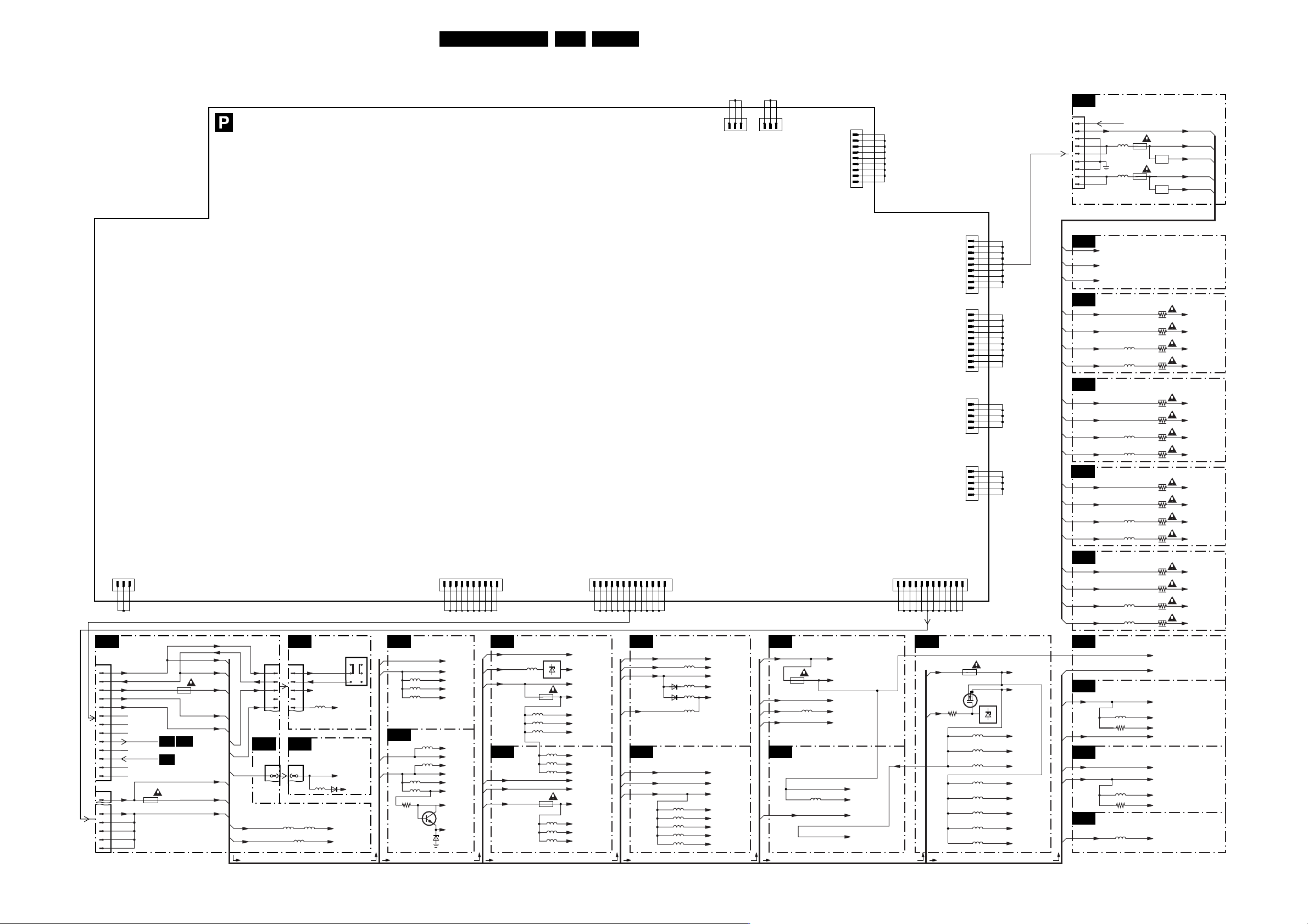
Power Lines Overview
21FM242 AA 6.
SC8
0319
0305
1
2
3
4
5
6
7
8
9
10
11
12
13
1
8
9
10
11
12
8004
AC LINE
3
VCC
NC
AC NEUTRAL
1
CONTROL FUNCTIONS 2
+9V-STBY
+9V-STBY-SW
+8V6
+5V-STBY-SW
+3V3-STBY-SW
POWER O.K.
SC7
STAND-BY
SC7
1100
T1A
+3V3
1105
500mA
SC13
OTC
+9V-STBY
+9V-STBY-SW
+8V6
+5V-STBY-SW
+3V3-STBY-SW
+5V-POW
+3V3
POWER SUPPLY PANEL
LED / SWITCH PANEL
LD
0320
+5V
+5V-STBY-SW
+8V6
+5V-STBY-SW
+5V
+5V_STBY_SW
0320
10
9
8
7
6
10
9
8
7
6
VGASC6
03180318
321
5541
+9V-STBY
+9V-STBY-SW
+5V-STBY-SW
5008
VGA CONNECTOR
5901
35305530
1101
6916
+5V REF
+5V_EXP
ON/OFF
SWITCH
1
2
3
+8V6
+5V-STB-SW
+5V
TO FANS
1
8006
NC
GND
FAN_SP
PDP-SUPPLY
(BLACKBOX)
_ON
D3.3V1
8009
10
PDP ASSYFROM MAINS-INLET
SYNC SELECTION
SC2
4
5
6
+3V3-STBY-SW
+5V
5007
5060
5009
SC3
+5V
+8V6
5140
5164
3164
VIDEO SELECTION
&MATRIX
5170
5167
7165
6166
+5V
+5A
+5B
6-7009
+5M
+5V
+8SW
+8V6
+8AA
+8A
VREF1
VREF2
GND
PDP_GO
RSV
V
GND
SC4
SC5
1
+5V-STBY-SW
+5V-POW
+3V3
VIDEO SELECTION - ADC
7175
5197
LD1117
1170
500mA
5196
5198
5199
VIDEO
+8V6
+5V
1270
+3V3
500mA
5220
5222
5224
5221
5223
5228
+5V_STBY_SW
+3V3PLL
+3V3
+3V3-AD
+3V3MAIN1
+3V3OUTPUT
+3V3MAIN2
3V3AA
3V3DB
3V3DD
+8V6
+5V
+3V3VID
3V3DA
3V3DC
3V3DE
S
D5V
D3.3V1
GND
GND
+9V_STBY_SW
+9V_STBY
8002
13
+3V3_STBY_SW
+5V_STBY_SW
8V6
SCL-1
SDA-1
POWER_OK
GND
SC6
+5V
SC7
RES
STANDBY
FAN_SP_2
FAN_SP_1
1
VGA INPUT
+5V
5300
+8V6
+5V-STBY-SW
6302
5302
5350
6353
5352
CONTROL FUNCTIONS 1 OTC
+5V
+8V6
+3V3-STBY-SW
5520
5521
5522
5523
5524
+5V
+8B
+5V-STBY-SW
+5S
+5R
+5V
+8V6
+3V3-STBY-SW
+3V3-CNTL-A
+3V3-CNTL-B
+3V3-CNTL-C
+3V3-CNTL-D
+3V3-CNTL-E
8005
1
NC
GND
fAN_SP
SCALER, CLOCK-GENERATOR
SC9
+3V3
1575
500mA
+3V3-STBY-SW
+5V
+5V-STBY-SW
SCALER-PW164 + MEMORY
SC10
+3V3
5572
5630
8007
Va
NC
Vcc
GND
GND
GND
NC
Vs
Vs
Vs
+3V3
+3V3-PW
+3V3-STBY-SW
+5V-OE
+5V-STBY-SW
+3V3-PW
+3V3W
+3V3
+2V5
9
PDP
ASSY
1
8003
VSND_NEG
VSND_NEG
GND_SND
GND_SND
VSND_POS
VSND_POS
GND_SND
9V_STBY
DC_PROT
8008
D5V
V
G
DND
SCAN
V
GND
V
SET
GND
GND
S
V
V
S
8010
V
A
V
A
NC
GND
GND
8011
V
A
V
A
NC
GND
GND
8001
5V
GND
12
GND
GND
SC11
GND
GND
+3V3
+8V6
GND
3V3
3V3
3V3
3V3
3V3
BACK-END-EPLD
1670
500mA
D
7641
3640
G
TL431
1
5642
5643
5644
5645
5646
5647
5648
5649
(IF VALID)
1
9
1
PDP
ASSY
10
1
PDP
ASSY
5
1
N.C.
5
+3V3-PLD
S
7640
+2V5
+2V5PLDA
+2V5PLDB
+2V5PLDC
+3V3PLDA
+3V3PLDB
+3V3PLDC
+3V3PLDD
+3V3PLDE
SUPPLY & DC PROTECTION
A7
0302
9
8
7
6
5
4
3
2
1
FILTERS
A2
+9V-STBY
VCC-10-POS
VCC-10-NEG
AUDIO AMPLI LEFT HIGH
A3
VCC-10-POS
VCC-10NEG
VSDN-POS
VSDN-NEG
AUDIO AMPLI LEFT LOW
A4
VCC-10-POS
VCC-10-NEG
VSDN-POS
VSDN-NEG
AUDIO AMPLI RIGHT HIGH
A5
VCC-10-POS
VCC-10-NEG
VSDN-POS
VSDN-NEG
AUDIO AMPLI LEFT LOW
A6
VCC-10-POS
VCC-10-NEG
VSDN-POS
VSDN-NEG
BACK-END-LVDS
SC12
AUDIO SOURCE SELECT
SC13
+8V6
+9V-STBY
AUDIO-PROCESSOR
SC14
+5V
+8V6
AUDIO-DELAY-LINE
SC15
+5
DC-PROT
5796
3796
5810
3810
5870
5335
5725
5335
5360
5435
5460
5535
5560
5635
5660
1730
2A5
7735,7736
STAB
1740
2A5
7745,7746
STAB
3315
3318
3330
????
3415
3418
3430
3455
3515
3518
3530
3555
3615
3618
3630
3655
+3V3-PW
+3V3-STBY-SW
+8V6
+8V6A
+4V3A
+9V-STBY
+5V
+8V6
+8V6B
+4V3B
+5D
CL 36532011_018.eps
+9V-STBY
VSDN-POS
VCC-10-POS
VSDN-NEG
VCC-10-NEG
8-7315
1-7315
C-7330
C-7335
8-7415
1-7415
C-7430
C-7455
8-7515
1-7515
C-7530
C-7555
8-7615
1-7615
C-7630
C-7655
200303
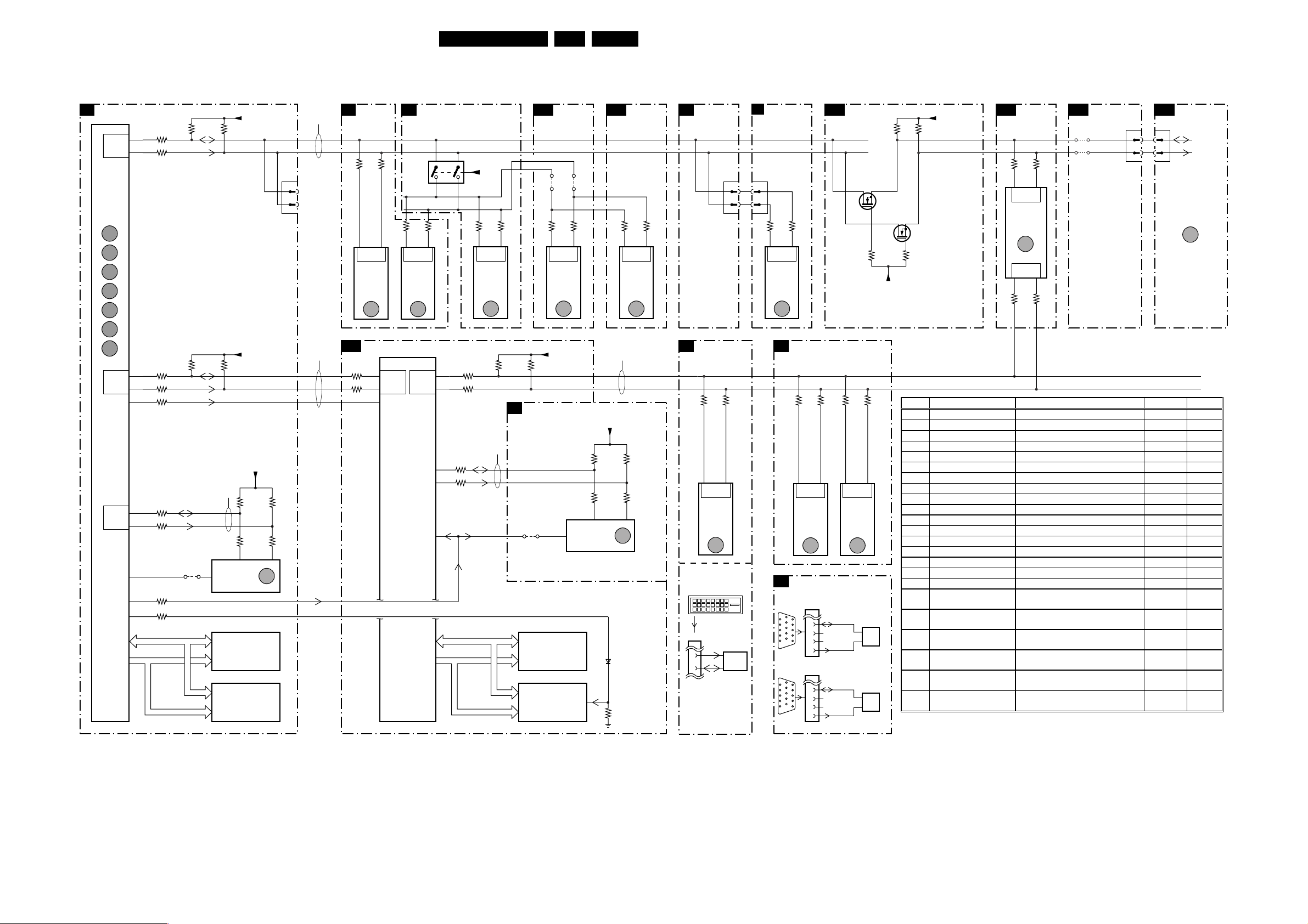
I2C-IC Overview
IIC
CONTROL
SC7
FUNCTIONS 1
86
MASTER
HW IIC
85
7383
SAA5801H
OTC
MAIN-
PROCESSOR
(MASTER)
ERR
91
ERR
92
ERR
93
ERR
94
ERR
95
ERR
96
ERR
97
88
SLAVE
HW IIC
87
91
MASTER
HW IIC
92
74
108
109
Block Diagrams, Testpoint Overviews, and Wiring Diagram
CONTROL
RESET
3404-C
3404-D
3404-A
3404-B
3398-C
3402-B
3402-A
3384
3007
ADDRESS
ADDRESS
DATA
3414 3415
3410 3413
IIC BUS 4
SDA_NVM_1
SCL_NVM_1
4431
7
PW_RESET
PW_FLASH_RESET
MSM51V18165F
DATA
+5V_STBY_SW
SDA-1
SCL-1
+3V3_CNTR_D
SDA-2
SCL-2
PW_START
+3V3_CNTL_D
3432
3433 3431
5
7430
M24C32
(NVM)
EEPROM
7500
RAM
7506
FLASH
0382
10
SERVICE
COMPAIR
CONNECTION
3430
6
ERR
7
9
IIC BUS 1
(slow 100KHz)
IIC BUS 2
(slow 100KHz)
SC8
3541
SC10
3608
3606
FUNCTIONS 2
3540
15
SLAVE
HW IIC
7540
PCF8574AT
I/O EXP.
ERR
PW164
3
A4
D6
E2
14
MASTER
SW
IIC
EXT INT
PROCESSOR
SCALER
SC9
9
PCF8591
7605
PW164
CO-
FOR
AND
OSD
7571
3532
SLAVE
HW IIC
7530
ADC
ERR
MASTER
CLOCK
GENERATOR
1
15
3531
10
4
B1
SW
C2
IIC
A1
C4
E3
3
4
3602
3603
GENERATOR
3604
3605
PW_RESET
DATA
ADDRESS
ADDRESS
+5V
1
SLAVE
HW IIC
7570
FS6377
CLOCK
ERR
IIC BUS 5
5
DATA
SC14
SCL_SW
SDA_SW
35703571
16
3601 3600
NVM
SC9
PW_SDA_NVM
PW_SCL_NVM
4581
M29W160DT
AUDIO
PROC.
13
SLAVE
HW IIC
MSP3415G
AUDI O
PROC.
+3V3_PW
7628
CY62126
RAM
7630
FLASH
7812
ERR
7
22FM242 AA 6.
SOURCE
SC13
SELECT
48104811
SCL_AUDIO
SDA_AUDIO
38123813
12
2
IIC BUS 3
(slow 100KHz)
+3V3_PW
3583
3582 3581
5
7580
M24C32
(NVM)
EEPROM
6630
3633
28
SLAVE
HW IIC
7798
TEA6422Q
MATRIX
SWITCH
ERR
3580
6
ERR
8
37943795
27
1
PW_SDA
PW_SCL
SC8
SC4
0375
6
7
CONTROL
FUNCTIONS2
VIDEO-SEL.
ADC
92
SLAVE
HW IIC
7170
AD9887KS
ADC +
TMDS REC.
ERR
10
DVI-D INPUT SOCKET
SCL
SDA
0319
6
7
32103209
91
7215
ST24FC21
DDC
EPROM
PROTECTION
P3
0319
6
7
PCF8574A
74
SLAVE
HW IIC
7370
I/O EXP.
ERR
6
SC5
VCA
VGA1 IN
15P"D"SHELL
CONNECTOR
11
12
13
14
15
VGA2 IN/OUT
15P"D"SHELL
CONNECTOR
11
12
13
14
15
33703371
73
VIDEO-SEL.
DECODER
3250
P10
SLAVE
HW IIC
7225
SAA7118E
VIDEO
DECODER
ERR
VGA
CONNECTOR
0371
6
1
7
12
2
8
3
13
9
4
10
14
5
15
0372
6
1
7
12
2
8
3
13
9
4
10
14
5
15
9
SC12
3251
N9
DCC-SDA-1
DCC-SCL-1
DCC-SDA-2
DCC-SCL-2
BACK-END
LVDS OUTPUT
SDA-1
SCL-1
7676
BSN20
DS
G
3284
21
SLAVE
HW IIC
7280
SDA9400
DE-
INTERLACER
ERR
11
7904
ST24FC21
5
DDC
7
NVM
7907
ST24FC21
5
DDC
7
NVM
7675
BSN20
DS
G
+3V3_STBY_SW
3285
20
36863682
+3V3_STBY_SW
36853681
SDA-1_3V3
SCL-1_3V3
SC11
EP1K30FC256
BACK-END
EPLD
3664
C5 C4
SLAVE
IIC
7656
EPLD
ERR
12
SLAVE
IIC
C8
C6
3663 3661
3662
SC12
4680
4684
BACK-END
LVDS OUTPUT
0301
16
18
PLASMA DISPLAY
PDP
PANEL
6
7
SDA-1_3V3
SCL-1_3V3
ERR
30
PW_SDA
PW_SCL
Error Device Description Item Diagr.
1
TEA6422D Audio switch (only
2
MSP3451G Sound processor 7812 SC14
3
PCF8574-SCAVIO I/O expander SCAVIO 7540 SC8
4
PCF8591 AD-DA expander 7530 SC8
5
FS6377 Clock generator 7570 SC9
6
PCF8574-PSU I/O expander PSU 7370 P3
7
24C16 OTC NVM OTC 7430 SC7
8
24C16 PW NVM PW 7580 SC9
9
SAA7118 Video decoder
10
AD9887 ADC/TMDS receiver 7170 SC4
11
SDA9400 De-interlacer (only
12
EP1K30QC EPLD processor 7656 SC11
13
PDP I2C error of the PDP
20
Download comm. Errors during downloading
21
CSP comm. CSP time-out error
40
Temperature alarm Detections of over-temperature
70
Over voltage Vs, Va, +5V, +3V3 overvoltage
(only
Enhanced
Enhanced
Enhanced
) 7798 SC13
) 7225 SC5
) 7280 SC5
Black
P
box
71
Vs under voltage Vs under voltage Black
P
box
72
Va under voltage Va under voltage Black
P
box
73
+5V under voltage +5V under voltage Black
P
box
74
+3V3 under voltage +3V3 under voltage Black
P
box
75
DC-PROT Audio amplifier protection Black
P
box
HW = HARDWARE
SW = SOFTWARE
CL 36532011_019.eps
210303
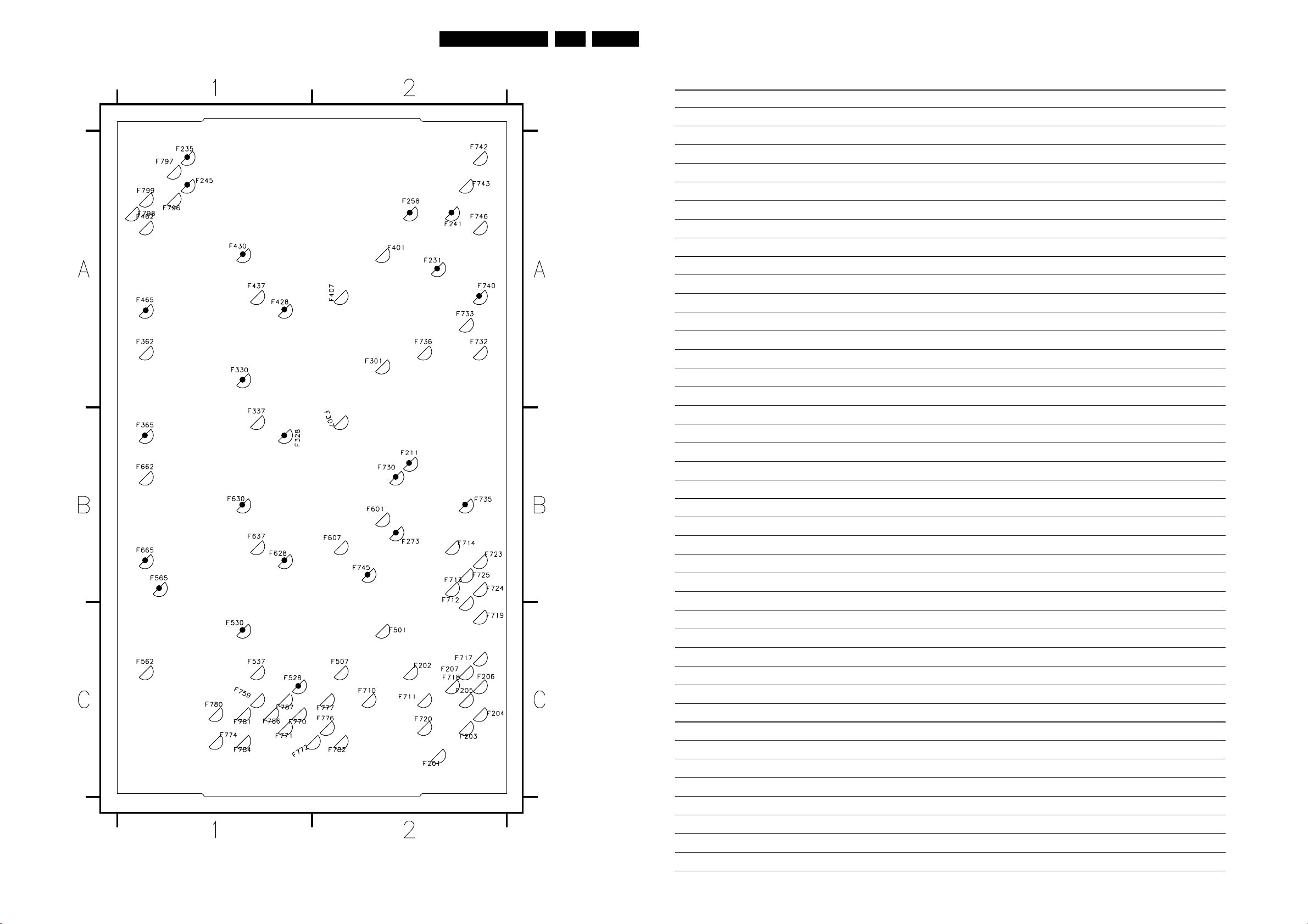
Block Diagrams, Testpoint Overviews, and Wiring Diagram
Testpoint Overview: Audio Amplifier Panel
23FM242 AA 6.
Personal Notes:
CL 26532038_024.eps
150402
F201 C2
F201 C2
F202 C2
F202 C2
F203 C2
F203 C2
F204 C2
F204 C2
F205 C2
F205 C2
F206 C2
F206 C2
F207 C2
F207 C2
F211 B2
F211 B2
F231 A2
F231 A2
F235 A1
F235 A1
F241 A2
F241 A2
F245 A1
F245 A1
F258 A2
F258 A2
F273 B2
F273 B2
F301 A2
F301 A2
F307 B2
F307 B2
F328 B1
F328 B1
F330 A1
F330 A1
F365 B1
F365 B1
F401 A2
F401 A2
F407 A2
F407 A2
F428 A1
F428 A1
F430 A1
F430 A1
F465 A1
F465 A1
F501 C2
F501 C2
F507 C2
F507 C2
F528 C1
F528 C1
F530 C1
F530 C1
F565 B1
F565 B1
F601 B2
F601 B2
F607 B2
F607 B2
F628 B1
F628 B1
F630 B1
F630 B1
F665 B1
F665 B1
F710 C2
F710 C2
F711 C2
F711 C2
F712 B2
F712 B2
F713 B2
F713 B2
F714 B2
F714 B2
F717 C2
F717 C2
F718 C2
F718 C2
F719 C2
F719 C2
F720 C2
F720 C2
F723 B2
F723 B2
F724 B2
F724 B2
F725 B2
F725 B2
F730 B2
F730 B2
F732 A2
F732 A2
F733 A2
F733 A2
F735 B2
F735 B2
F736 A2
F736 A2
F740 A2
F740 A2
F742 A2
F742 A2
F743 A2
F743 A2
F745 B2
F745 B2
F746 A2
F746 A2
F759 C1
F759 C1
F770 C1
F770 C1
F771 C1
F771 C1
F772 C1
F772 C1
F774 C1
F774 C1
F776 C2
F776 C2
F777 C2
F777 C2
F780 C1
F780 C1
F781 C1
F781 C1
F782 C2
F782 C2
F784 C1
F784 C1
F786 C1
F786 C1
F787 C1
F787 C1
F796 A1
F796 A1
F797 A1
F797 A1
F798 A1
F798 A1
F799 A1
F799 A1
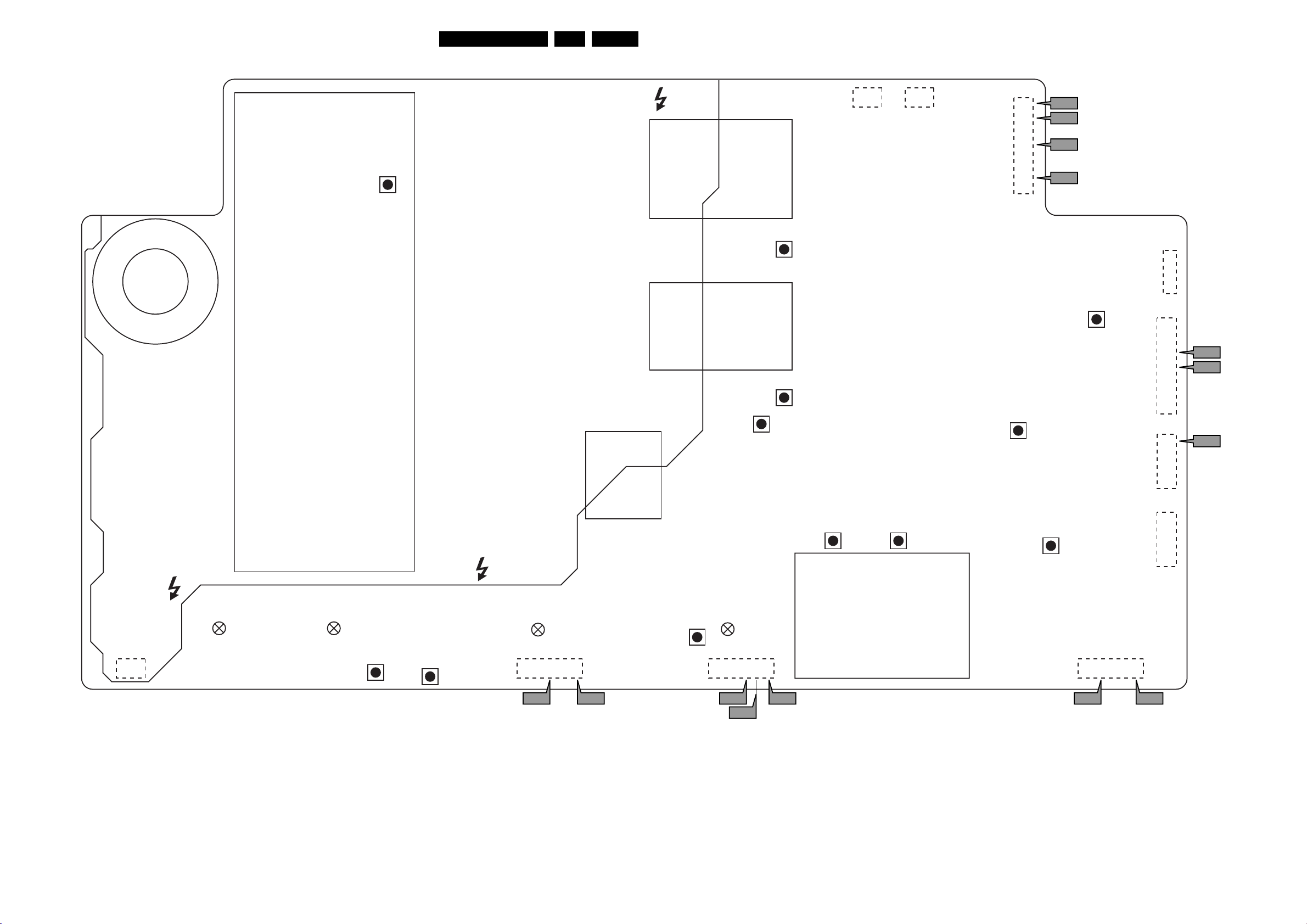
Block Diagrams, Testpoint Overviews, and Wiring Diagram
Testpoint Overview: Power Supply
24FM242 AA 6.
PFC
VR8001
COIL
COIL
8005
13
8007
VSCAN
1
2
5
8
9
P8
P9
P10
P11
VE
VR8005
8003
8008
1
4
5
10
1
9
P12
P13
COLDHOT
VS
VR8008
VA
VR8010
Vcc
13
8006
HOT
8004
COIL
VR8009
8V6 VFAN
VR8007 VR8006
VR8004
VSET
VR8003
HOT
COLD
GREEN
8001
13
COLD
GREEN
8002
5V_STBY_S
VR8002 VR8011
3V3_VSB_S
GREEN
8003
8009
1510
P7 P6 P2 P1
VR8012
DV5
RED
8004
8002
13413
P5 P3
P4
COMPONENT SIDE
Protection
Board
8001
CL 36532011_009.eps
8010
8011
1812
1
5
1
5
200303
P14
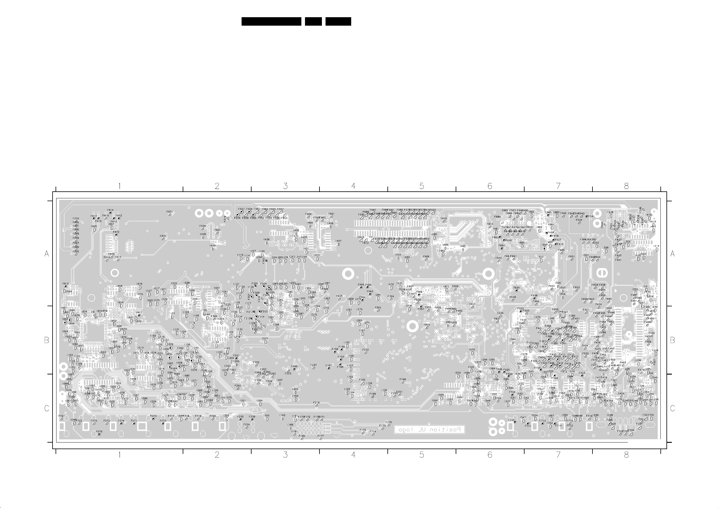
Block Diagrams, Testpoint Overviews, and Wiring Diagram
Testpoint Overview: SCAVIO Panel
F070 C1
F177 C4
F225 A1
F251 B2
F312 B2
F383 B7
F401 B7
F070 C1
F071 C1
F071 C1
F072 C1
F072 C1
F073 C1
F073 C1
F074 C1
F074 C1
F075 C1
F075 C1
F076 C1
F076 C1
F089 B1
F089 B1
F146 B4
F146 B4
F152 B4
F152 B4
F158 B4
F158 B4
F170 C5
F170 C5
F171 C4
F171 C4
F172 C3
F172 C3
F173 C3
F173 C3
F174 C4
F174 C4
F175 C4
F175 C4
F176 C4
F176 C4
F177 C4
F178 C3
F178 C3
F180 C3
F180 C3
F181 C3
F181 C3
F196 B4
F196 B4
F197 B4
F197 B4
F198 C5
F198 C5
F199 C4
F199 C4
F201 C5
F201 C5
F202 B4
F202 B4
F203 C5
F203 C5
F210 C3
F211 C3
F216 C3
F216 C3
F220 C3
F220 C3
F221 B2
F221 B2
F222 B3
F222 B3
F223 B3
F223 B3
F224 C3
F224 C3
F225 A1
F226 A1
F226 A1
F227 A1
F227 A1
F228 A1
F228 A1
F229 A1
F229 A1
F230 A1
F230 A1
F231 A1
F231 A1
F232 A1
F232 A1
F233 A1
F233 A1
F234 C2
F234 C2
F235 C2
F235 C2
F236 C3
F236 C3
F237 B3
F237 B3
F240 B3
F241 B3
F242 B3
F245 B5
F246 B5
F247 B5
F249 B3
F249 B3
F250 B2
F250 B2
F251 B2
F260 C2
F260 C2
F261 B3
F261 C3
F262 B3
F262 C3
F263 B3
F263 B3
F264 B3
F264 C3
F265 B3
F265 C3
F300 A4
F300 A4
F301 B4
F301 B4
F303 A3
F303 A3
F304 A3
F304 A3
F305 A3
F305 A3
F306 A3
F306 A3
F307 A2
F307 A3
F308 A3
F308 A3
F309 A3
F309 A3
F310 A3
F310 A3
F311 A3
F311 A3
F312 B3
F313 B3
F313 B3
F314 B3
F314 B3
F315 B2
F315 B2
F316 B3
F316 B3
F317 B3
F317 B3
F318 B3
F318 B3
F319 A2
F319 A2
F320 C8
F320 C8
F321 C8
F321 C8
F322 C8
F322 C8
F323 B3
F323 B3
F324 A5
F324 A5
F325 A2
F325 A2
F326 B2
F326 B2
F380 A7
F380 A7
F381 A7
F381 A7
F382 A8
F382 A8
F383 C7
F384 B7
F384 B7
F385 B7
F385 B7
F386 B7
F386 B7
F387 B7
F387 B7
F388 B7
F388 B7
F389 B7
F389 B7
F390 B7
F390 B7
F391 B7
F391 B7
F392 B7
F392 B7
F393 B7
F393 B7
F394 B7
F394 B7
F395 B7
F395 B7
F396 B7
F396 B7
F397 B7
F397 B7
F398 B7
F398 B7
F399 B7
F399 B7
F400 B7
F400 B7
F401 B7
F402 B7
F402 B7
F403 B7
F403 B7
F404 B7
F404 B7
F405 B7
F405 B7
F406 B7
F406 B7
F407 B7
F407 B7
F408 B7
F408 B7
F409 B7
F409 B7
F410 B7
F410 B7
F411 B7
F411 B7
F412 B7
F412 B7
F413 B7
F413 B7
F414 B7
F414 B7
F415 B7
F415 B7
F416 B7
F416 B7
F417 B7
F417 B7
F418 B7
F418 B7
F419 B7
F419 B7
F420 B8
F420 B8
F421 B7
F421 B7
F422 B8
F422 B8
F423 B7
F423 C7
F424 B7
F424 B7
F425 B6
F425 B6
F426 B6
F426 C6
F427 A7
F427 A7
F428 A7
F428 A7
F429 C8
F429 C8
F430 B6
F430 B6
F431 B7
F431 B7
F432 B8
F432 B8
F450 A8
F450 A8
F451 A8
F451 A8
F452 A8
F452 A8
F453 A8
F453 A8
F459 C8
F459 C8
F460 B8
F460 B8
F461 B8
F461 B8
F462 B8
F462 B8
F463 B8
F463 B8
F464 B8
F464 B8
F465 B8
F465 B8
F466 B8
F466 B8
F467 B8
F467 B8
F468 B8
F468 B8
F469 B8
F469 B8
F470 B8
F470 B8
F471 B8
F471 B8
F472 B8
F472 B8
F473 B8
F473 B8
F474 B8
F474 B8
F475 B8
F475 B8
F476 B8
F476 B8
F477 C8
F477 C8
F478 B8
F478 B8
F479 C8
F479 C8
F480 A8
F480 A8
F481 A8
F481 A8
F482 B8
F482 B8
F483 B8
F483 B8
F484 B8
F484 B8
F485 B8
F485 B8
F486 B8
F486 B8
F487 B8
F487 B8
F488 B8
F488 B8
F489 B8
F489 B8
F490 B7
F490 B7
F492 B8
F492 B8
F493 B8
F493 B8
F494 B8
F494 B8
F495 B8
F495 B8
F496 B8
F496 B8
F497 A8
F497 A8
F506 B8
F507 B8
F507 B8
F520 B6
F520 B6
F521 B7
F521 B7
F522 B7
F522 B7
F523 B7
F523 B7
F524 B8
F524 B8
F525 B6
F526 B6
F529 A7
F529 A7
F530 A8
F530 A8
F531 A8
F531 A8
F532 A8
F532 A8
F533 A8
F533 A8
F534 A8
F534 A8
F535 A8
F535 A8
F536 A8
F536 A8
F537 A8
F537 A8
F538 A8
F538 A8
F539 A8
F539 A8
F540 A7
F540 A7
F541 A7
F541 A7
F542 A7
F542 A7
F543 A7
F543 A7
F544 A7
F544 A7
F545 A7
F545 A7
F546 A2
F546 A2
F547 A2
F547 A2
F548 A2
F548 A2
F549 A2
F549 A2
F550 A3
F550 A3
F551 A3
F551 A3
F552 A3
F552 A3
F553 A3
F553 A3
F554 A3
F554 A3
F555 A3
F555 A3
F556 A3
F556 A3
F557 A3
F557 A3
F558 A3
F558 A3
F559 A3
F559 A3
F560 A4
F560 A4
F561 A4
F561 A4
F562 A3
F562 A3
F563 A4
F563 A4
F564 A4
F564 A4
F565 A4
F565 A4
F566 A4
F566 A4
F567 A5
F567 B5
F568 A5
F568 A5
F569 A5
F569 A5
F570 A5
F570 A5
F571 A5
F571 A5
F572 A5
F572 A5
F573 A5
F573 A5
F574 A5
F574 A5
F575 A5
F575 A5
F576 A5
F576 A5
F577 A5
F577 A5
F578 A5
F578 A5
F579 A5
F579 A5
F580 A5
F580 A5
F581 A5
F581 A5
F582 A5
F582 A5
F583 A4
F583 A4
F584 A4
F584 A4
F585 A4
F585 A4
F586 A4
F586 A4
F587 A4
F587 A4
F588 A4
F588 A4
F589 A4
F589 A4
F590 A4
F590 A4
F591 A5
F591 A5
F592 A5
F592 A5
F593 A5
F593 A5
F594 A5
F594 A5
F595 A5
F595 A5
F596 A5
F596 A5
F597 A5
F597 A5
F598 A5
F598 A5
F599 A5
F599 A5
F600 A5
F600 A5
F601 A5
F601 A5
F602 A5
F602 A5
F603 A5
F603 A5
F604 A5
F604 A5
F605 A5
F605 A5
F606 A4
F606 A4
F607 A4
F607 A4
F608 A4
F608 A4
F609 A4
F609 A4
F610 A4
F610 A4
F611 A4
F611 A4
F612 A4
F612 A4
F613 A4
F613 A4
F614 A6
F614 A6
F615 A7
F615 A7
F616 A7
F616 A7
F617 A5
F618 B4
F619 B5
F620 B5
F621 B4
F622 A5
F622 A5
F623 A6
F623 B6
F624 B5
F624 B5
F625 B5
F625 B5
F626 B5
F626 B5
F627 A5
F627 A5
F628 A4
F628 A4
F629 A5
F629 A5
F630 A5
F630 A5
F631 A5
F631 A5
F632 A5
F632 A5
F633 B5
F634 A6
F634 A6
F635 B5
F635 B5
F636 B6
F636 B6
F637 B6
F637 B6
F638 A7
F638 A7
F639 B6
F639 B6
F640 A8
F640 A8
F641 A6
F641 A6
F642 A8
F642 A8
F643 A7
F643 A7
F644 A8
F644 A8
F645 A7
F645 A7
F646 A7
F646 A7
F647 A6
F647 A6
F648 A6
F648 A6
F649 B7
F649 B7
F650 A7
F650 A7
F651 A7
F651 A7
F652 A6
F652 A6
F653 A7
F653 A7
F654 A8
F654 B8
F655 A8
F655 A8
F656 A7
F656 A7
F657 A8
F657 A8
F658 A8
F658 A8
F659 A8
F659 A8
F660 B6
F660 B6
F661 B5
F661 B5
F662 B5
F662 B5
F670 A7
F670 A7
F671 A7
F671 A7
F672 A6
F672 A6
F673 A6
F673 A6
F674 A6
F674 A6
F675 A6
F675 A6
F676 A6
F676 A6
F677 A6
F677 A6
F678 A6
F678 A6
F679 A6
F679 A6
F680 A7
F680 A7
F681 A6
F681 A6
F682 A6
F682 A6
F683 A6
F683 A6
F684 A6
F684 A6
F685 A6
F685 A6
F686 A6
F686 A6
F690 A6
F690 A6
F691 A6
F691 A6
F692 A6
F692 A6
F710 C6
F710 C6
F711 C7
F711 C7
F712 C7
F712 C7
F713 C7
F713 C7
F714 C7
F714 C7
F715 C7
F715 C7
F716 C7
F716 C7
F717 C1
F717 C1
F718 C2
F718 C2
F719 C2
F719 C2
F720 C2
F720 C2
F721 C1
F721 C1
F722 C1
F722 C1
F723 B7
F723 B7
F724 C6
F724 C6
F725 C6
F725 C6
F810 A1
F810 A1
F811 B1
F811 B1
F812 A1
F812 A1
F813 A1
25FM242 AA 6.
F813 A1
F814 A1
F814 A1
F815 A1
F815 A1
F816 A1
F816 A1
F817 A1
F817 A1
F820 B1
F820 B1
F870 A1
F870 A1
F871 A1
F871 A1
F872 A1
F872 A1
F873 A1
F873 A1
F874 A1
F874 A1
F875 A1
F875 A1
I000 C1
I000 C1
I001 A2
I001 A2
I002 C1
I002 C1
I003 C1
I003 C1
I004 B1
I004 B1
I005 C1
I005 C1
I006 B1
I006 B1
I007 C1
I007 C1
I008 C1
I008 C1
I009 B1
I009 B1
I010 C1
I010 C1
I011 B1
I011 B1
I012 C1
I012 C1
I013 C1
I013 C1
I014 B1
I014 B1
I015 B3
I015 B3
I016 A5
I016 B5
I017 A1
I017 A1
I018 B1
I018 B1
I019 B1
I019 B1
I020 B1
I020 B1
I021 A1
I021 A1
I022 A1
I022 A1
I023 B1
I023 B1
I024 B1
I024 B1
I025 A1
I025 A1
I026 A2
I026 A2
I027 A1
I027 A1
I028 B8
I028 B8
I029 A1
I029 A1
I030 B1
I030 B1
I031 B1
I031 B1
I032 B1
I032 B1
I033 A1
I033 A1
I034 C1
I034 C1
I035 C1
I035 C1
I036 A5
I036 A5
I037 A5
I037 A5
I050 C2
I050 C2
I051 C2
I051 C2
I052 C2
I052 C2
I053 B2
I053 B2
I054 B1
I054 B1
I055 B1
I055 B1
I056 C1
I056 C1
I057 C1
I057 C1
I058 B1
I058 B1
I059 C1
I059 C1
I060 C1
I060 C1
I061 B2
I061 B2
I062 C2
I062 C2
I063 C1
I063 C1
I064 B1
I064 B1
I065 B1
I065 B1
I066 C1
I066 C1
I067 C1
I067 C1
I068 C1
I068 C1
I069 B2
I069 B2
I070 C1
I070 C1
I071 C2
I071 C2
I072 B2
I072 B2
I073 B2
I073 B2
I074 B2
I074 B2
I075 B2
I075 B2
I076 C2
I076 C2
I077 C1
I077 C1
I078 B1
I078 B1
I079 C1
I079 C1
I080 C2
I080 C2
I081 C1
I081 C1
I082 C1
I082 C1
I083 B1
I083 B1
I084 C3
I084 C3
I085 B1
I085 C1
I086 C1
I086 C1
I087 C1
I087 C1
I088 C1
I088 C1
I100 C2
I100 C2
I101 B2
I101 B2
I102 B1
I102 B1
I103 B1
I103 B1
I104 B1
I104 B1
I105 C2
I105 C2
I106 B2
I106 C2
I107 C2
I107 C2
I108 B2
I108 B2
I109 B1
I109 B1
I110 B1
I110 B1
I111 B1
I111 B1
I112 B2
I112 B2
I113 B2
I113 B2
I114 A2
I114 A2
I115 A2
I115 A2
I116 B1
I116 B1
I117 A2
I117 B2
I118 A2
I118 B2
I119 B2
I119 B2
I120 A2
I120 A2
I121 A2
I121 A2
I122 B1
I122 B1
I123 B2
I123 B2
I124 B2
I124 B2
I125 B2
I125 B2
I126 A2
I126 A2
I127 A2
I127 A2
I128 B2
I128 B2
I129 B3
I129 B3
I130 B2
I130 B2
I131 B1
I131 B1
I151 B4
I151 B4
I152 C4
I152 C4
I153 C4
I153 C4
I154 C4
I154 C4
I155 B4
I155 B4
I156 B4
I156 B4
I157 B4
I157 B4
I158 C4
I158 C4
I159 C4
I159 C4
I160 C3
I160 C3
I161 C3
I161 C3
I162 C4
I162 C4
I165 C3
I165 C3
I166 C3
I166 C3
I200 C3
I200 C3
I201 C2
I201 C2
I202 C2
I202 C2
I203 C3
I203 C3
I204 A3
I204 A3
I205 B2
I205 B2
I206 B2
I206 B2
I220 A2
I220 B2
I221 C8
I221 C8
I222 C8
I222 C8
I223 C8
I223 C8
I224 B2
I224 B2
I225 B8
I225 B8
I226 B8
I226 C8
I227 C8
I227 C8
I228 B8
I228 B8
I229 C8
I229 C8
I230 A8
I230 A8
I231 A8
I231 B8
I232 A8
I232 A8
I233 B8
I233 C8
I234 C8
I234 C8
I235 C8
I235 C8
I236 C8
I236 C8
I237 C8
I237 C8
I238 B8
I238 B8
I239 A8
I239 A8
I240 B8
I240 B8
I241 A8
I241 A8
I242 A3
I242 A3
I243 A3
I243 A3
I244 A3
I244 A3
I245 C8
I245 C8
I246 C8
I246 C8
I247 A3
I247 A3
I248 A3
I248 A3
I249 C8
I249 C8
I250 A3
I250 A3
I251 A3
I251 A3
I252 C8
I252 C8
I253 A3
I253 A3
I254 A3
I254 A3
I255 A3
I255 A3
I256 C8
I256 C8
I257 C8
I257 C8
I258 A3
I258 B3
I259 A3
I259 A3
I260 A3
I260 A3
I261 A3
I261 A3
I262 A3
I262 A3
I263 A4
I263 A4
I264 A4
I264 A4
I265 A3
I265 A3
I266 B3
I266 B3
I267 A4
I267 A4
I268 A4
I268 A4
I269 A4
I269 A4
I270 B4
I270 B4
I271 A3
I271 B3
I272 B4
I272 B4
I273 B7
I273 B7
I274 A4
I274 A4
I275 B4
I275 B4
I276 B3
I276 B3
I277 B6
I277 B6
I278 A3
I278 A3
I279 B6
I279 C6
I280 A3
I280 A3
I281 B4
I281 B4
I282 A3
I282 A3
I283 A3
I283 A3
I284 B6
I284 B6
I285 B3
I285 B3
I286 B3
I286 B3
I287 B3
I287 B3
I288 A3
I288 A3
I289 B6
I289 B6
I290 B6
I290 B6
I291 B3
I291 B3
I292 B6
I292 B6
I293 B4
I293 B4
I294 B3
I294 B3
I295 B8
I295 B8
I296 B5
I296 B5
I344 B6
I344 B6
I345 B6
I345 B6
I346 B7
I346 B7
I347 B7
I347 B7
I348 B7
I348 B7
I349 B7
I349 B7
I350 B6
I350 B6
I351 B6
I351 B6
I352 A8
I352 A8
I353 B7
I353 B7
I354 C7
I354 C7
I355 C7
I355 C7
I356 C8
I356 C8
I357 C7
I357 C7
I358 A8
I358 A8
I359 C8
I359 C8
I360 C7
I360 C7
I361 C8
I361 C8
I362 C8
I362 C8
I363 B7
I363 B7
I364 B7
I364 B7
I365 C8
I365 C8
I366 B7
I366 B7
I400 A7
I400 A7
I401 A3
I401 A3
I402 A3
I402 A3
I405 A3
I405 A3
I406 A4
I406 A4
I407 A4
I407 A4
I408 A2
I408 A2
I409 A2
I409 A2
I430 A5
I430 A5
I431 A5
I431 A5
I432 A5
I432 A5
I433 A5
I433 A5
I435 A3
I435 A3
I436 A3
I436 A3
I480 A5
I480 A5
I481 A6
I481 A6
I482 A5
I482 A5
I483 A5
I483 A5
I485 A6
I485 A6
I486 A5
I486 A5
I501 A7
I501 A7
I502 A8
I502 A8
I503 A8
I503 A8
I504 A7
I504 A7
I505 A7
I505 A7
I506 A7
I506 A7
I507 A7
I507 A7
I530 C6
I530 C6
I531 C6
I531 C6
I532 C6
I532 C6
I533 C1
I533 C1
I534 C1
I534 C1
I535 B6
I535 C6
I536 B6
I536 C6
I537 C6
I537 C6
I538 C1
I538 C1
I539 C1
I539 C1
I540 C1
I540 C1
I541 C7
I541 C7
I542 C7
I542 C7
I543 C7
I543 C7
I544 C1
I544 C1
I545 B7
I545 C7
I546 C7
I546 C7
I547 C6
I547 C6
I548 C7
I548 C7
I549 C6
I549 C6
I550 C7
I550 C7
I551 B7
I551 C7
I552 B7
I552 C7
I553 C5
I553 C5
I554 C7
I554 C7
I555 C5
I555 C5
I556 C5
I556 C5
I557 C2
I557 C2
I558 C2
I558 C2
I559 C7
I559 C7
I560 C2
I560 C2
I561 C6
I561 C6
I562 C7
I562 C7
I563 C7
I563 C7
I564 C7
I564 C7
I565 C2
I565 C2
I566 C2
I566 C2
I567 C7
I567 C7
I568 C2
I568 C2
I569 C6
I569 C6
I570 B6
I570 C6
I571 C7
I571 C7
I572 C7
I572 C7
I573 C7
I573 C7
I574 C6
I574 C6
I575 C6
I575 C6
I576 C1
I576 C1
I577 C1
I577 C1
I578 C7
I578 C7
I579 B7
I579 C7
I580 C7
I580 C7
I581 C1
I581 C1
I582 C6
I582 C6
I583 C8
I583 C8
I584 C6
I584 C6
I585 C6
I585 C6
I586 C1
I586 C1
I587 C1
I587 C1
I588 B6
I588 C6
I589 C6
I589 C6
I590 C7
I590 C7
I591 C8
I591 C8
I592 C6
I592 C6
I593 C8
I593 C8
I594 C8
I594 C8
I595 C6
I595 C6
I596 B6
I596 C6
I597 C1
I597 C1
I598 C7
I598 C7
I599 C6
I599 C6
I650 B1
I650 B1
I651 B1
I651 B1
I652 B1
I652 B1
I653 B1
I653 B1
I654 A1
I654 B1
I655 B1
I655 B1
I656 B1
I656 B1
I657 A1
I657 A1
I658 A1
I658 A1
I659 B1
I659 B1
I660 B1
I660 B1
I661 B1
I661 B1
I662 B1
I662 B1
I663 B1
I663 B1
I664 B1
I664 B1
I665 A1
I665 A1
I666 A1
I666 A1
I667 B1
I667 B1
I668 B1
I668 B1
I669 B1
I669 B1
I670 B1
I670 B1
I671 B1
I671 B1
I672 B1
I672 B1
I673 B1
I673 B1
I674 B1
I674 B1
I675 A1
I675 A1
I676 A1
I676 A1
CL 26532038_51t.eps
150402
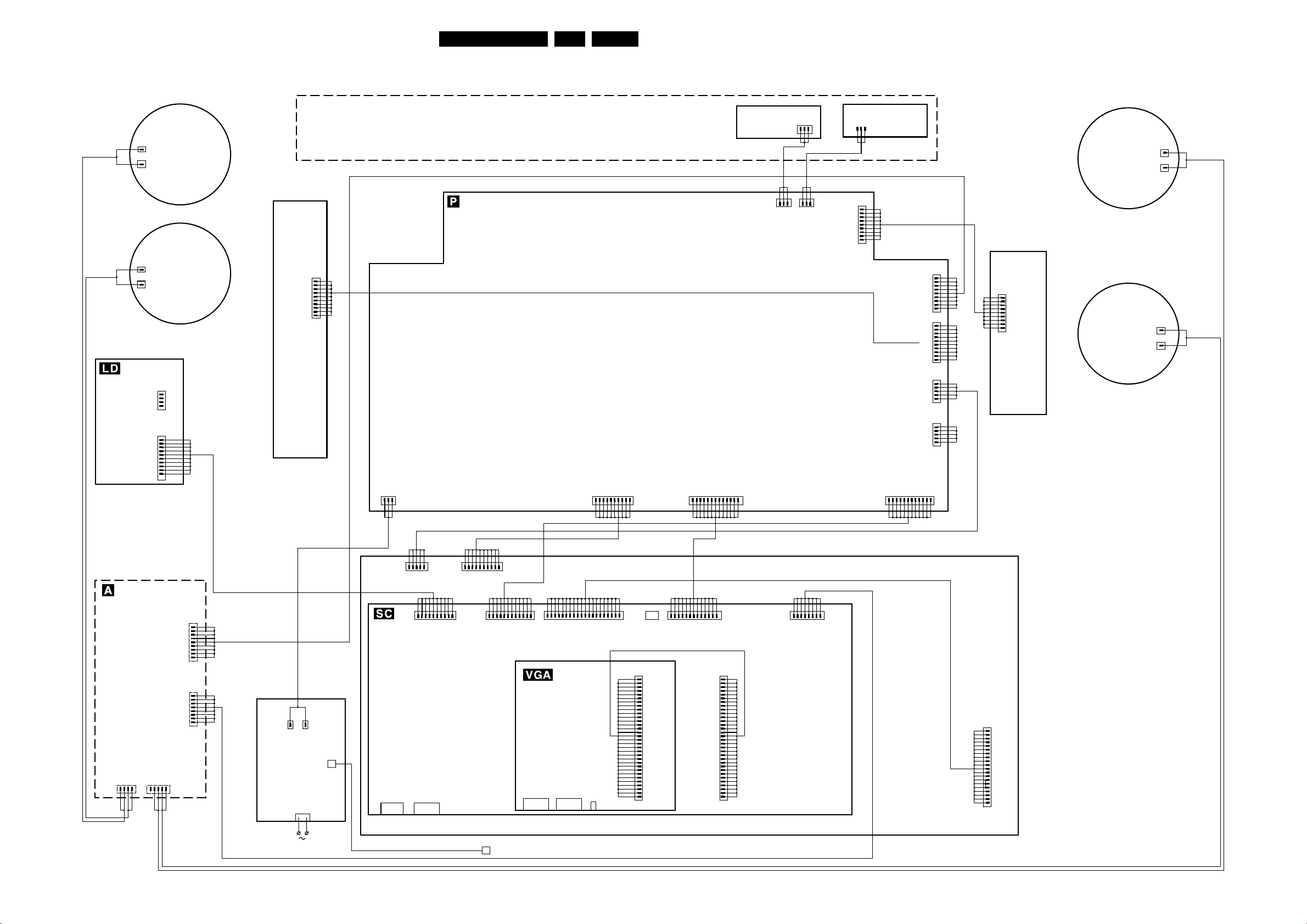
Block Diagrams, Testpoint Overviews, and Wiring Diagram
Wiring Diagram
26FM242 AA 6.
-
+
-
+
LED / SWITCH
PANEL
POS 1072
LIGHT_SENSOR_IN
RC_IN_ICONN
RED_LED
RC_OUT_ICONN
GND
+5V_STBY
GREEN_LED
RED_LED
RC_IN
+8V6
GND
+5V_STBY_SW
+9V_STBY_SW
+9V_STBY
0317
0320
LSP
RIGHT
HIGH
LSP
RIGHT
LOW
1
1
PDP
YM
CN805
FAN
(IF VALID)
1
(IF VALID)
1
FAN
OPTIONAL
LSP
LEFT
HIGH
-
+
1
GND
FAN_SP
1
8005
NC
GND
fAN_SP
8007
Va
1
NC
Vcc
GND
GND
GND
NC
Vs
Vs
Vs
9
PDP
8003
1
VSND_NEG
VSND_NEG
GND_SND
GND_SND
VSND_POS
VSND_POS
GND_SND
9V_STBY
DC_PROT
9
8008
1
D5V
V
G
DND
V
SCAN
GND
SET
V
GND
GND
V
S
V
S
10
8010
1
V
A
V
A
NC
GND
GND
5
8011
1
V
A
V
A
NC
GND
GND
5V
3V3
3V3
3V3
GND
GND
GND
GND
GND
GND
8001
12
N.C.
5
3V3
3V3
1
XM
CN804
LSP
LEFT
LOW
-
+
POWER SUPPLY PANEL
1
10
8006
NC
PDP-SUPPLY
(BLACKBOX)
_ON
8004
AC LINE
3
NC
AC NEUTRAL
1
S
D5V
D3.3V1
GND
GND
D3.3V1
V
GND
RSV
GND
PDP_GO
8009
10
1
8002
13
+9V_STBY
+9V_STBY_SW
+3V3_STBY_SW
+5V_STBY_SW
8V6
SCL-1
SDA-1
GND
STANDBY
POWER_OK
FAN_SP_1
RES
FAN_SP_2
1
AUDIO AMPLIFIER
PANEL (IF VALID)
POS 1050
VSND_NEG
VSND_NEG
VSND_POS
VSND_POS
+9V_STBY
DC_PROT
AUDIO_RIGHT_NEG
AUDIO_RIGHT_POS
RIGHT_GND
AUDIO_ENABLE
LEFT_GND
AUDIO_LEFT_NEG
AUDIO_LEFT_POS
LOW_RIGHT_POS
HIGH_RIGHT_POS
LOW_RIGHT_NEG
HIGH_RIGHT_NEG
0304
1
HIGH_LEFT_POS
N.C.
0303
LOW_LEFT_POS
LOW_LEFT_NEG
HIGH_LEFT_NEG
5
PDP E-BUFFER / F-BUFFER / G-BUFFER / LOGIC BOARD
1
CN806
10
9 pole
D-shell
0320
RED_LED
+5V_STBY
GREEN_LED
4x CINCH
0302
1
GND
GND
GND
0388
1
GND
1
0308
BLUE
MAINS_NEUTRAL
MAINS-inlet
+ Filter
POS 1061
BROWN
MAINS_LIVE
M91
SCAVIO
PANEL
POS 1063
GND
+8V6
RC_IN
+9V_STBY
+9V_STBY_SW
+5V_STBY_SW
LIGHT_SENSOR_IN
10
D3.3V1
D3.3V1
1
1
CN803
D5V
_ON
RSV
GND
GND
GND
GND
S
V
PDP_GO
1
12
0305
5V
GND
GND
1
0301
3V3
3V3
3V3
3V3
3V3
GND
GND
GND
GND
RXIN0-
RXIN0+
GND_LVDS
SCL0
RXIN1-
GND
RXIN1+
SDA0
RXIN2-
RXIN2+
CPU-GO
GND_LVDS
VGA CONNECTOR
PANEL
POS 1032
15 pole
D-shell
1x CINCH
CP91
15 pole
D-shell
PDP-GO
RXCLKIN-
RXCLKIN+
20
IRQ
PDWN
RXIN3-
RXIN3+
GND_LVDS
0318
1
0315
foil
N.C.
+5V_STBY_SW
VGA2_OUTN
RC_OUT
GND
VGA2_RXD
VGA2_TXD
GND
VGA2_V
GND
VGA2_H
GND
VGA2_B
GND
VGA2_G
GND
VGA2_R
GND
RC_VGA1
GND
VGA1_RXD
VGA1_TXD
GND
VGA1_V
GND
VGA1_H
GND
VGA1_B
GND
VGA1_G
GND
VGA1_R
GND
1
0319
+9V_STBY
8V6
SCL-1
+9V_STBY_SW
+5V_STBY_SW
+3V3_STBY_SW
+5V_STBY_SW
RES
GND
SDA-1
POWER_OK
VGA2_OUTN
RC_OUT
GND
VGA2_RXD
VGA2_TXD
GND
VGA2_V
GND
VGA2_H
GND
VGA2_B
GND
VGA2_G
GND
VGA2_R
GND
RC_VGA1
GND
VGA1_RXD
VGA1_TXD
GND
VGA1_V
GND
VGA1_H
GND
VGA1_B
GND
VGA1_G
GND
VGA1_R
GND
STANDBY
FAN_SP_2
FAN_SP_1
0318
1
foil
1
0388
RIGHT_GND
AUDIO_ENABLE
AUDIO_RIGHT_POS
AUDIO_RIGHT_NEG
GND
LEFT_GND
AUDIO_LEFT_POS
AUDIO_LEFT_NEG
CN1
1
20
CL 36532011_001.eps
200303
Electrical Diagrams and PWB Layouts
7. Electrical Diagrams and PWB Layouts
Audio Panel & Supply: DC Protection
27FM242 AA 7.
A
B
C
D
E
F
G
0388
8
1
PH-S
GND_F
GND_F
AUDIO PANEL
& SUPPLY , DC PROTECTION
VCC_10_POS
VCC_10_NEG
+9V_STBYA
L_HIGH
L_HIGH
L_LOW
R_HIGH
R_LOW
L_LOW
AU_EN_NOT
R_HIGH
R_LOW
+9V_STBYA
VCC_10_POS
VCC_10_NEG
GND_F
L_POS
L_NEG
GND_F
AUDIO_ENABLE
GND_F
R_POS
R_NEG
DIAGRAM
GND
AU_EN_NOT
FILTERS
L_HIGH
AU_EN_NOT
L_LOW
AU_EN_NOT
AU_EN_NOT
R_HIGH
654321
L_HIGH
AU_EN_NOT
GND_I
GND_I
L_LOW
AU_EN_NOT
GND_I
GND_I
AU_EN_NOT
R_HIGH
GND_I
GND_I
VCC_10_POS
VCC_10_NEG
VCC_10_POS
VCC_10_NEG
VCC_10_POS
VCC_10_POS
VCC_10_NEG
VCC_10_POS
VCC_10_NEG VCC_10_NEG
VCC_10_POS
VCC_10_NEG
VCC_10_POS
VCC_10_NEG
7
AMPLIFIER LEFT_HIGH
DIAGRAM
GND
AMPLIFIER LEFT_LOW
DIAGRAM
AMPLIFIER RIGHT_HIGH
DIAGRAM
VSND_POS
VSND_NEG
VSND_POS
VSND_NEG
VSND_POS
VSND_NEG
VSND_POS
VSND_NEG
VSND_POS
VSND_NEG
VSND_POS
VSND_NEG
VSND_POS
VSND_NEG
GND_O
GND_O
GND_O
GND_O
GND_O
OUT_LH
OUT_PROT
GND_O
OUT_PROT
OUT_LL
OUT_RH
OUT_PROT
OUT_LH
OUT_LL
OUT_RH
OUT_PROT
1098
OUT_LH
OUT_LL
OUT_RH
OUT_RL
OUT_PROT
GND GND_O
VCC_10_POS
VCC_10_POS
0302
9
1
PH-S
VCC_10_NEG
VCC_10_NEG
DC_PROT
+9V_STBY
GND
VSND_POS
VSND_POS
GND
GND
VSND_NEG
VSND_NEG
+9V_STBYA
+9V_STBYA
VSND_POS
VSND_POS
OUT_RH
OUT_RL
SUPPLY & DC PROTECTION
DIAGRAM
GND_O
VSND_NEG
VSND_NEG
GND_O
OUT_LH
OUT_LL
GND_O
GND_O
GND_O
5
1
4
1
131211
A
B
C
0303
D
PH-S
E
0304
F
PH-S
G
H
AU_EN_NOT
R_LOW
AU_EN_NOT
VCC_10_POS
VCC_10_NEG
VSND_POS
VSND_NEG
OUT_PROT
OUT_RLR_LOW
OUT_RL
H
AMPLIFIER RIGHT_LOW
GND_I
I
GND_I
J
1
432 131211
5
6
DIAGRAM
7
GND_O
GND_O
I
J
CL 26532038_015.eps
290302
1098
 Loading...