

Panasonic TY-TP58P10S Service Manual
ORDER NO. ITD0802007CE
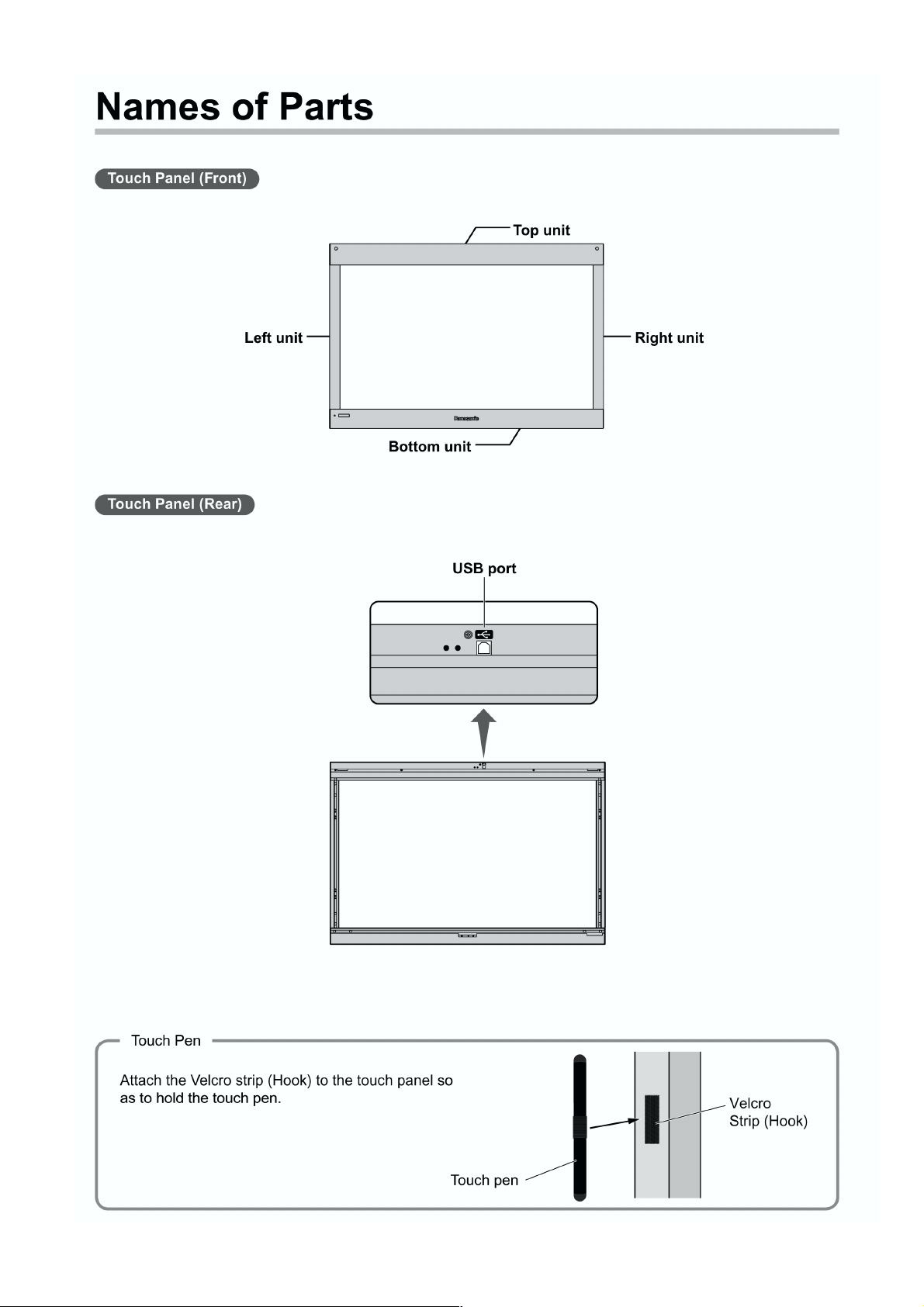
Touch Panel
Model No. TY-TP58P10S
TABLE OF CONTENTS
1 Warning-------------------------------------------------------------- 2
1.1. Prevention of Electrostatic Discharge (ESD)
to Electrostatically Sensitive (ES) Devices---------- 2
1.2. About lead free solder (PbF)---------------------------- 3
2 Specifications ----------------------------------------------------- 4
3 General/Introduction -------------------------------------------- 5
3.1. PCB Stracture---------------------------------------------- 5
4 Operating Instructions------------------------------------------6
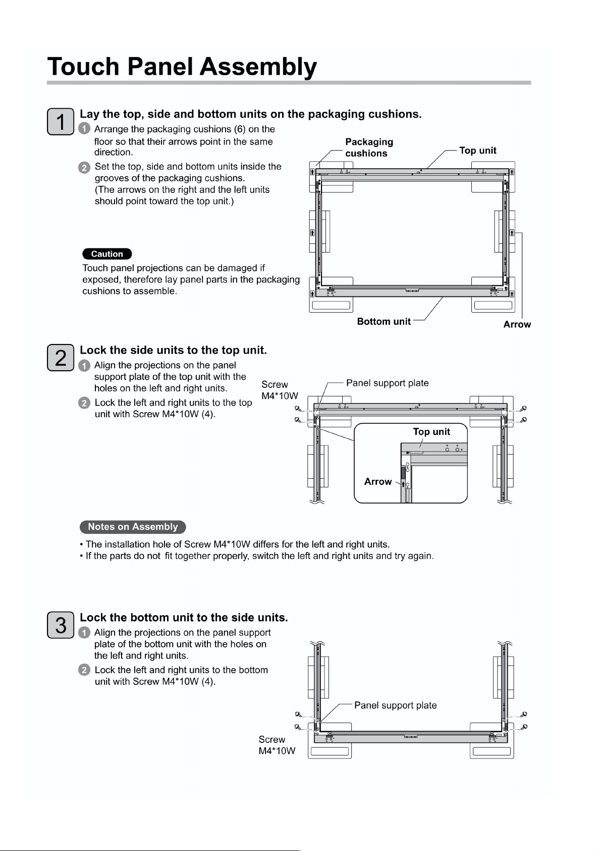
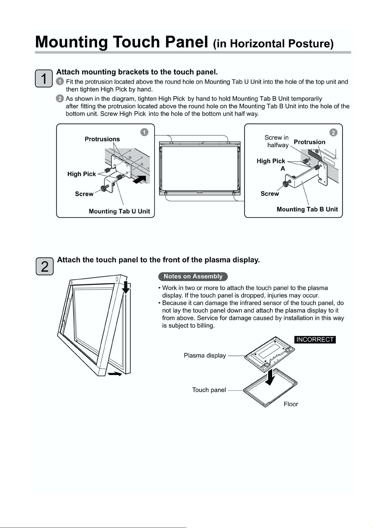
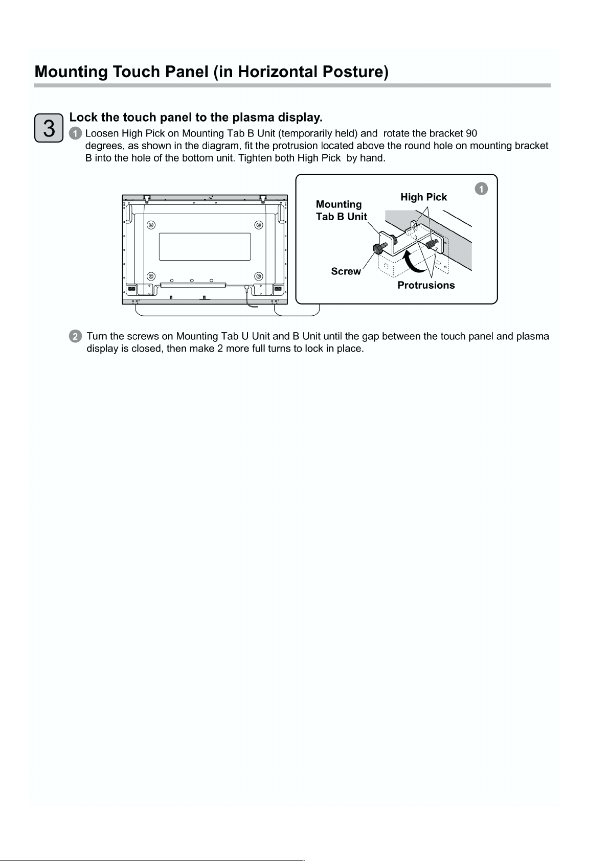
5 Disassembly and Assembly Instructions ---------------40
5.1. Remove the Frame U Assy ----------------------------40
5.2. Remove the Cover-U Assy-----------------------------40
5.3. Remove the Flat bracing metal -----------------------40
5.4. Remove the Main board unit---------------------------40
5.5. Remove the Sensor-L board unit---------------------40
5.6. Remove the Sensor-R board unit --------------------40
5.7. Remove the Right angle-UL ---------------------------41
5.8. Remove the Right angle-UR------------------- --------41
6 Measurements and Adjustments---------------------------42
PAGE PAGE
6.1. Before the adjustment when Circuit board are
exchanged------------------------------------------------- 42
6.2. Cautions for replacing the Circuit board------------ 42
6.3. Flow chart for replacing the Boards -----------------42
6.4. How to rewrite data when replacing the Main
Board-------------------------------------------------------- 43
6.5. Adjust the optical axis----------------------------------- 43
6.6. Adjust PEAKPOSI (Corner) --------------------------- 45
6.7. Setting range (first, last) of the optical axis--------46
6.8. Adjust and confirm the light level--------------------- 47
7 25-point calibration---------------------------------------------48
7.1. Prepare setting for adjusting PC--------------------- 48
7.2. Explanation of 25-point Calibration------------------48
8Dimensions-------------------------------------------------------51
9 Block Diagram --------------------------------------------------- 52
10 Schematic Diagram --------------------------------------------53
10.1. Main Board Unit Schematic Diagram ---------------53
10.2. Sensor Board Unit Schematic Diagram ------------54
© 2008 Matsushita Electric Industrial Co., Ltd. All
rights reserved. Unauthorized copying and distribution is a violation of law.

1Warning
1.1. Prevention of Electrostatic Discharge (ESD) to Electrostatically Sensitive (ES) De v ices
Some semiconductor (so lid st ate) devic es ca n be da ma ged ea sily by st a tic el ectric ity. Such component s com monl y ar e called Elec trostatically Sensitive (ES) Devices. Examples of typical ES devices are integrated circuits and some field-effect transistors and
semiconductor "chip" components. The following techniques should be used to help reduce the incidence of component damage
caused by electrostatic discharge (ESD).
1. Immediately before handling any semicon duc tor co mp on ent or se miconductor-equipped assembly, drain off any ESD on your
body by touching a kno w n ea rth g round. Alternatively , ob t ai n and wear a commercially available d is charging ESD wrist strap,
which should be removed for potential shock reasons prior to applying power to the unit under test.
2. After removing an electrical assembly equipped with ES devices, place the assembly on a conductive surface such as aluminum foil, to prevent electrostatic charge buildup or exposure of the assembly.
3. Use only a grounded-tip soldering iron to solder or unsolder ES devices.
4. Use only an anti-static solder removal device. Some solder removal devices not classified as "anti-static (ESD protected)"
can generate electrical charge sufficient to damage ES devices.
5. Do not use freon-propelled chemicals. These can generate electrical charges sufficient to damage ES devices.
6. Do not remove a replacement ES device from its protective package until immediately before you are ready to install it. (Most
replacement ES devices are p a ck ag ed wit h leads electrically shorted together by con du cti ve foam , al umi nu m fo il or c om p a r able conductive material).
7. Immediately before removing the protective material from the leads of a replacement ES device, touch the protective material
to the chassis or circuit assembly into which the device will be installed.
Caution
Be sure no power is applied to the chassis or circuit, and observe all other safety precautions.
8. Minimize bodily motions when hand ling u np ackage d rep lacemen t ES de vices. (Other wise ha m less mo tion s uch as the brus hing together of your clothes fabric or the lifting of your foot from a ca rpe ted fl oor can generate static electricity (ESD) sufficient
to damage an ES device).
2
1.2. About lead free solder (PbF)
Note: Lead is listed as (Pb) in the periodic table of elements.
In the information below, Pb will refer to Lead solder, and PbF will refer to Lead Free Solder.
The Lead Free Solder used in our manufacturing process and discussed below is (Sn+Ag+Cu).
That is Tin (Sn), Silver (Ag) and Copper (Cu) although other types are available.
This model uses Pb Free solder in it’s manufacture due to environmental conservation issues. For service and repair work, we’d
suggest the use of Pb free solder as well, although Pb solder may be used.
PCBs manufactured using lead free solder will have the PbF within a leaf Symbol PbF sta mped on the bac k of PCB.
Caution
• Pb free solder has a higher melting point t han st anda rd sold er. Typicall y the me lting p oin t is 50 ~ 7 0 °F (30~40 °C) hig her. Please
use a high temperature soldering iron and set it to 700 ± 20 °F (370 ± 10 °C).
• Pb free solder will tend to splash when heated too high (about 1100 °F or 600 °C).
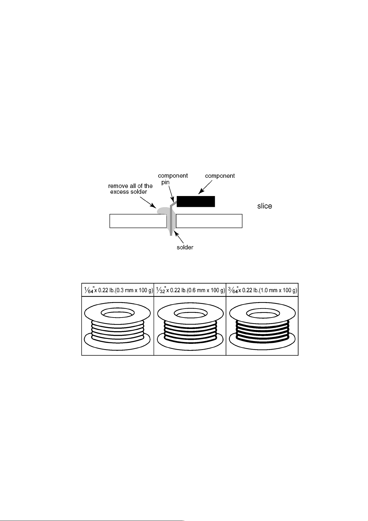
If you must use Pb solder, please completely remove all of the Pb free solder on the pins or solder area before applying Pb solder. If this is not practical, be sure to heat the Pb free solder until it melts, before applying Pb solder.
• After applying PbF solder to double lay ere d bo ards , p lea se che ck the co mp onent side for excess solder which may flo w onto the
opposite side. (see figure below)
Suggested Pb free solder
There are several kinds of Pb free solder available for purchase. This product uses Sn+Ag+Cu (tin, silver, copper) solder. However, Sn+Cu (tin, copper), Sn+Zn+Bi (tin, zinc, bismuth) solder can also be used.
3

2 Specifications
Type Touch Panel
Power source
Voltage +5V DC ± 10%
Electric current Max. 450 mA
Supply system From USB bus
Touch panel
Detection system Infrared retroreflective detection
Panel window
Detection range
Effective detection range Same as above
Resolution Approx. 32,000 × 18,000 points *1
Output system Coordinate output
Optic element pitch Infrared LED x 4, CMOS image sensor × 2
Minimum detection size
Response rate 100 points / sec
Interface
Temperature When operating: 0 ~ 70°C (0 ~ 40°C) *2
Humidity When operating: 20 ~ 80% (No dewing) *2
Resistance to external Lateral light 2,000 lx + 20% (20° angle of incidence)
light Frontal light 10,000 lx + 20% (90° angle of incidence)
External dimensions
Mass Approx. 15.65 lb. (7.1 kg)
Escutcheon material Aluminum
3
/8”(1,305 mm) (W) × 2927/64” (747.5 mm) (H)
51
43
50
/
“(1,287 mm) (W) × 2831/64” (723.5 mm) (H)
64
23
/64” (9 mm)
USB 2.0 full speed device
Signals: +DATA, -DATA, VCC, GND
Connector: Type B
15
/16” (1,395.4 mm) (W) × 3611/32” (923.1 mm) (H) × 157/64” (47.9 mm) (D)
54
*1 Resolution obtained by using a dedicated Driver software
*2 When the panel is attached to a Plasma display produced by Matsushit a Electric Industrial Co., Ltd.
4
3 General/Introduction
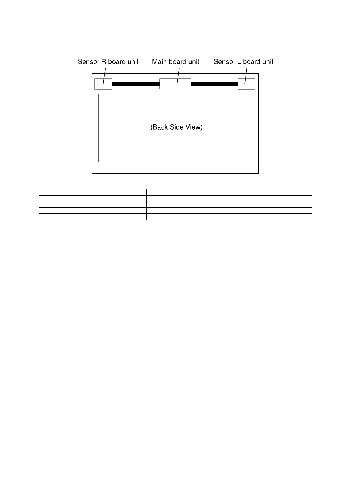
3.1. PCB Stracture
Unit Name Board Number Function Contained data Accompanying tasks
Main TXN/11WETB Main control Adjusted data Copying data, adjusting gain
Sensor-L TXN/22WETB IR sensor L - Adjusting the optical axis. ranee and gain
Sensor-R TXN/31WETB IR sensor R - Adjusting the optical axis, ranee and gain
(If copying is not available, all adjustment is necessary)
R-sensor Board and L-sensor Board emit and receive the infrared rays.
Each Board has the infrared LED and image sensor.
Control Board contains data including infrared rays signal. image sensor-receiving position, image sensor sensitivity and its range,
etc in eeprom.
Light receiving-data of left and right sensors is analyzed by this Board and the position is determined.
5
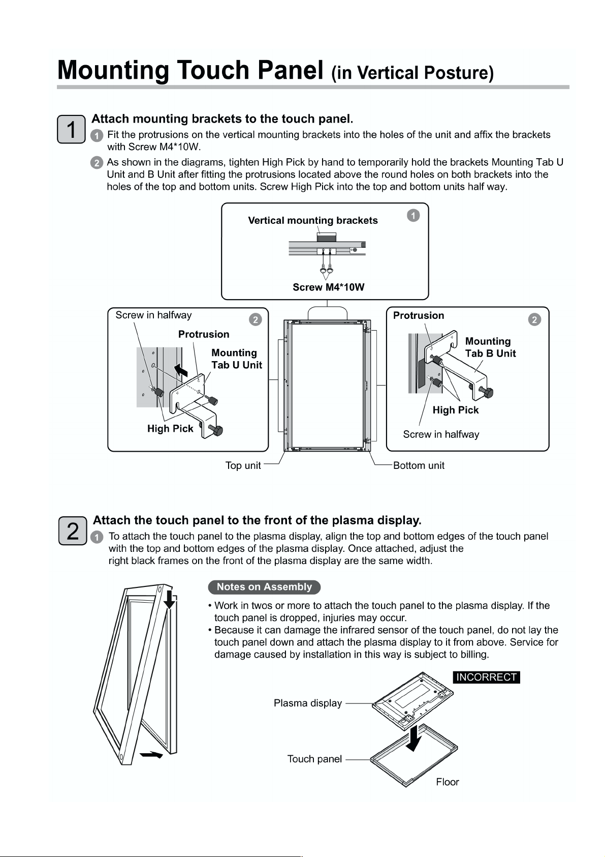
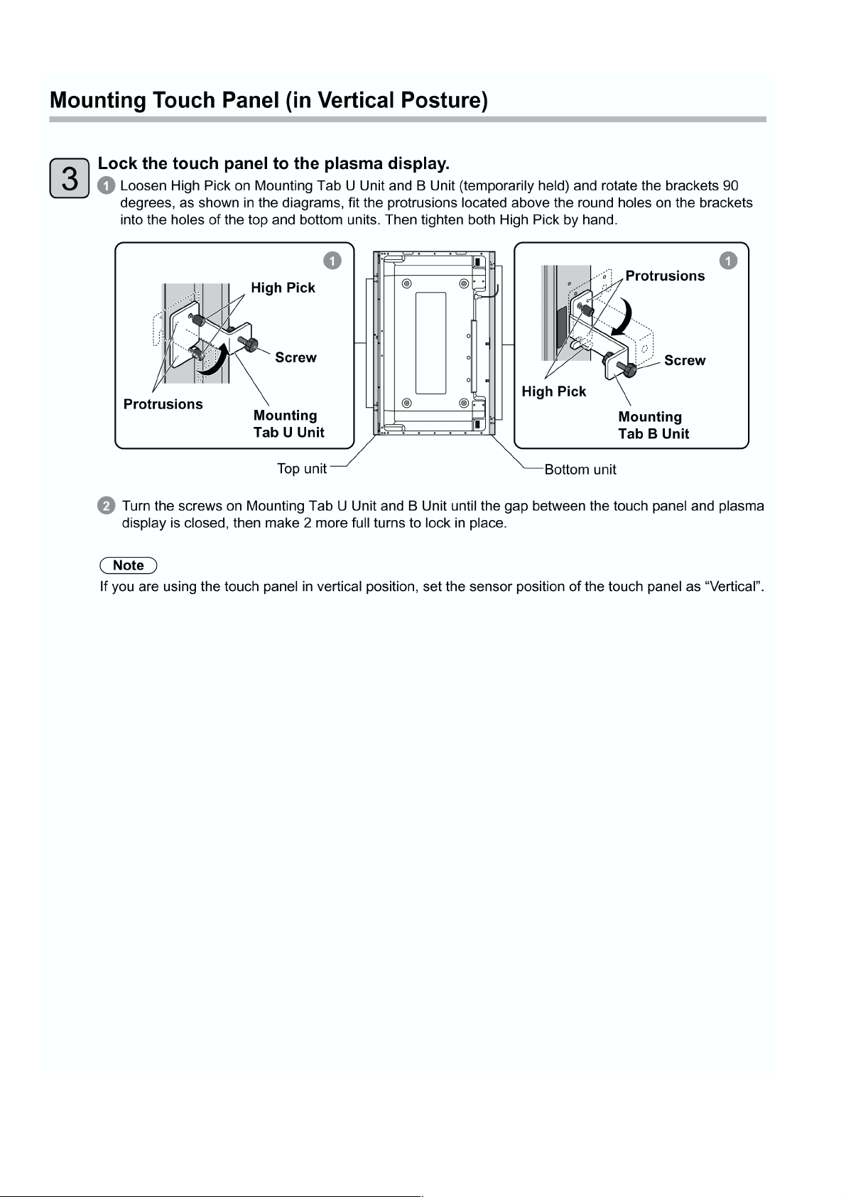
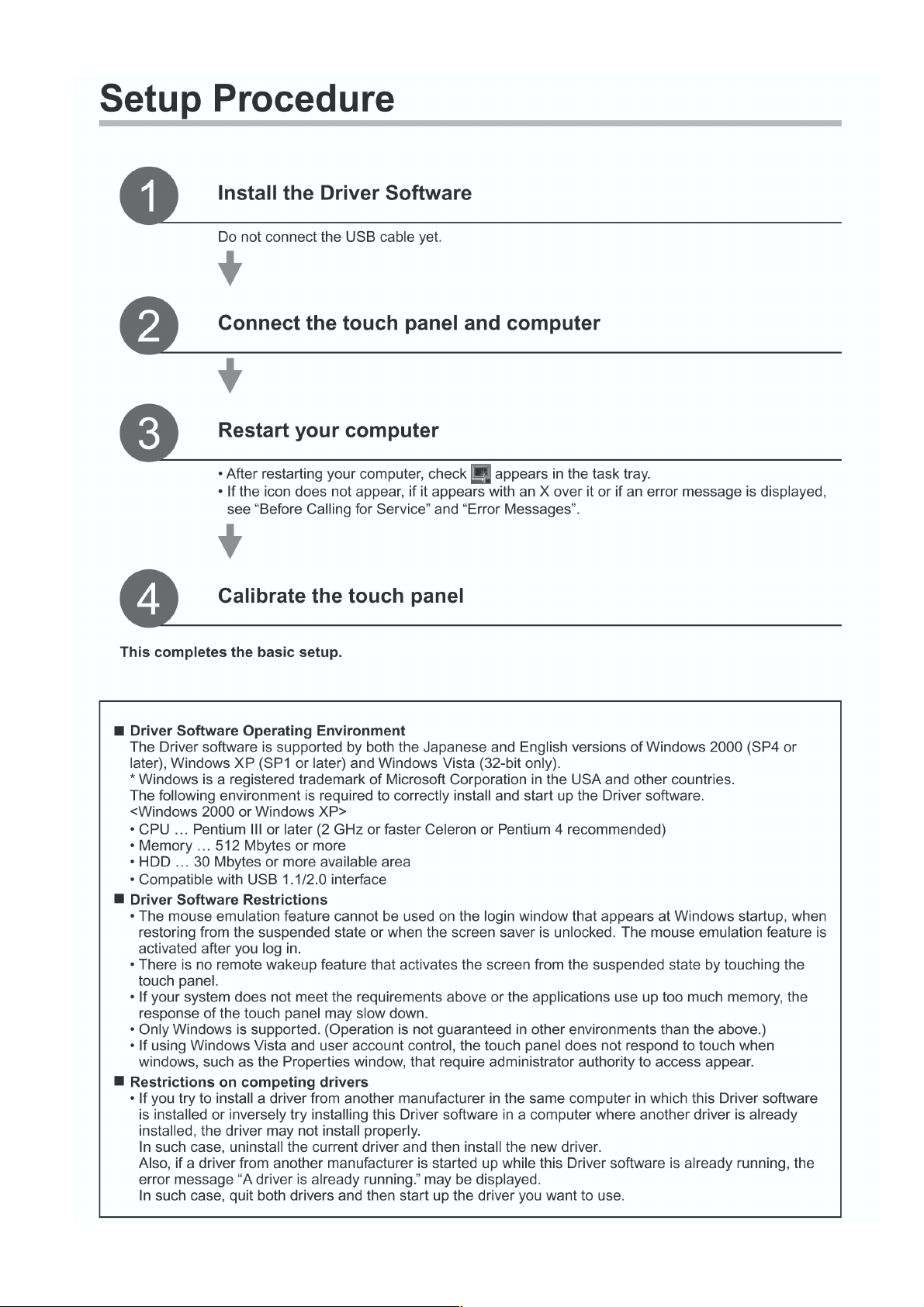
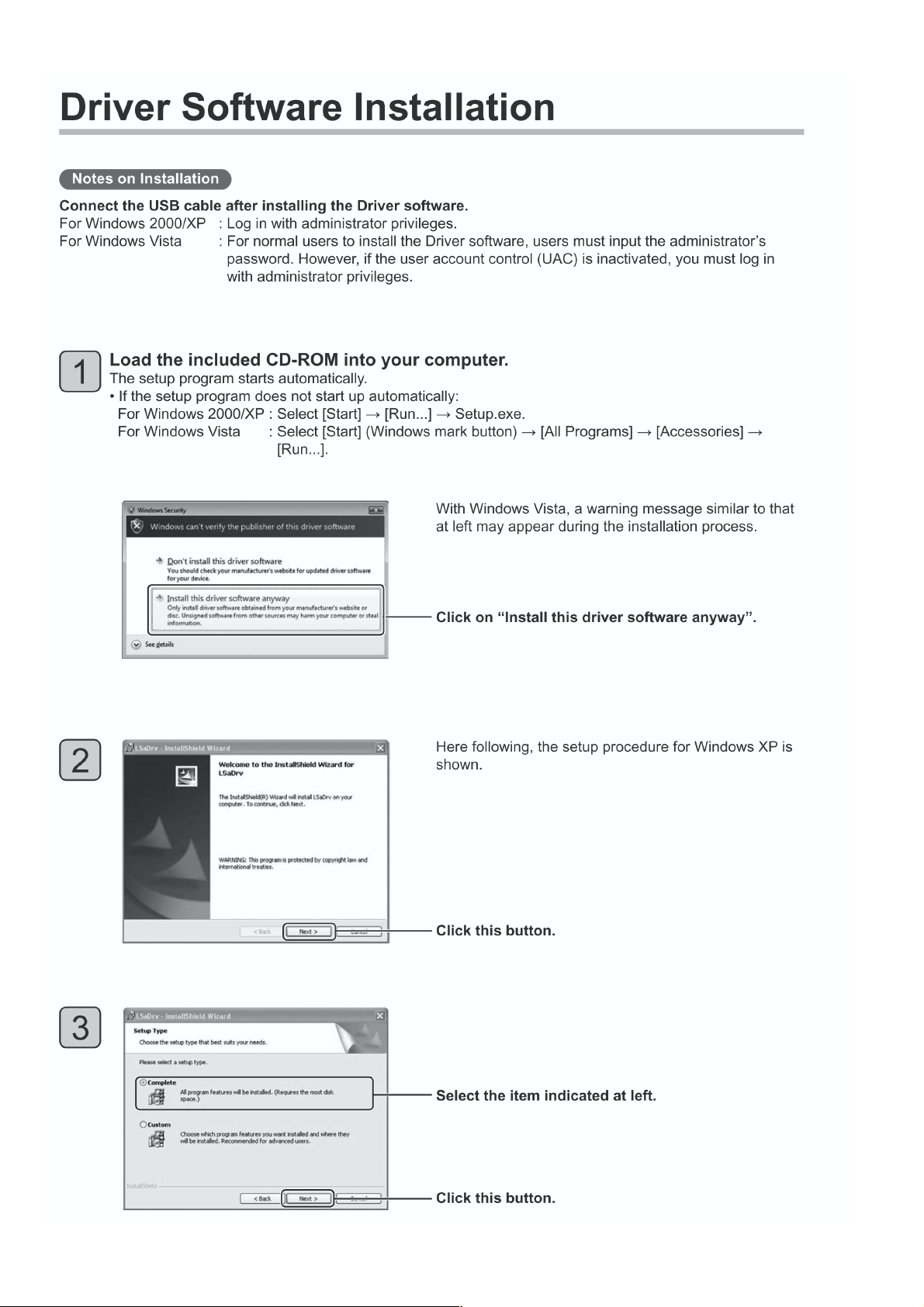
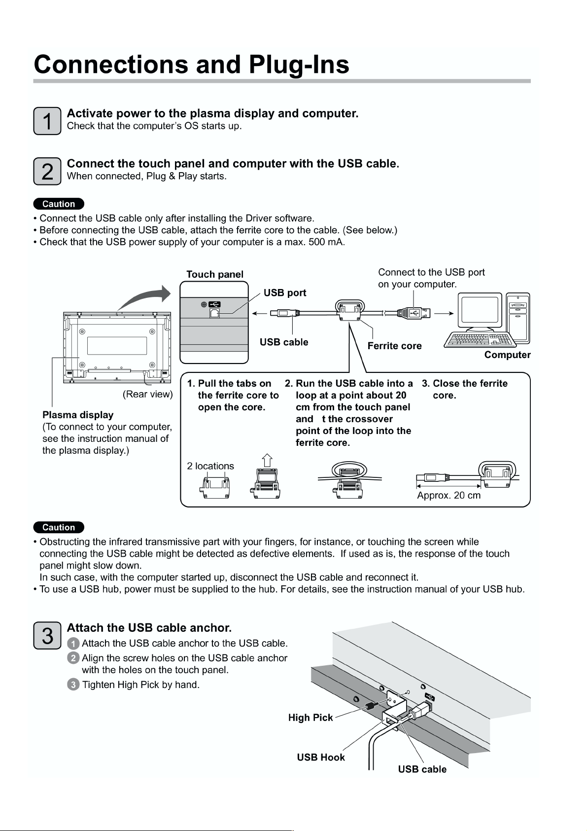
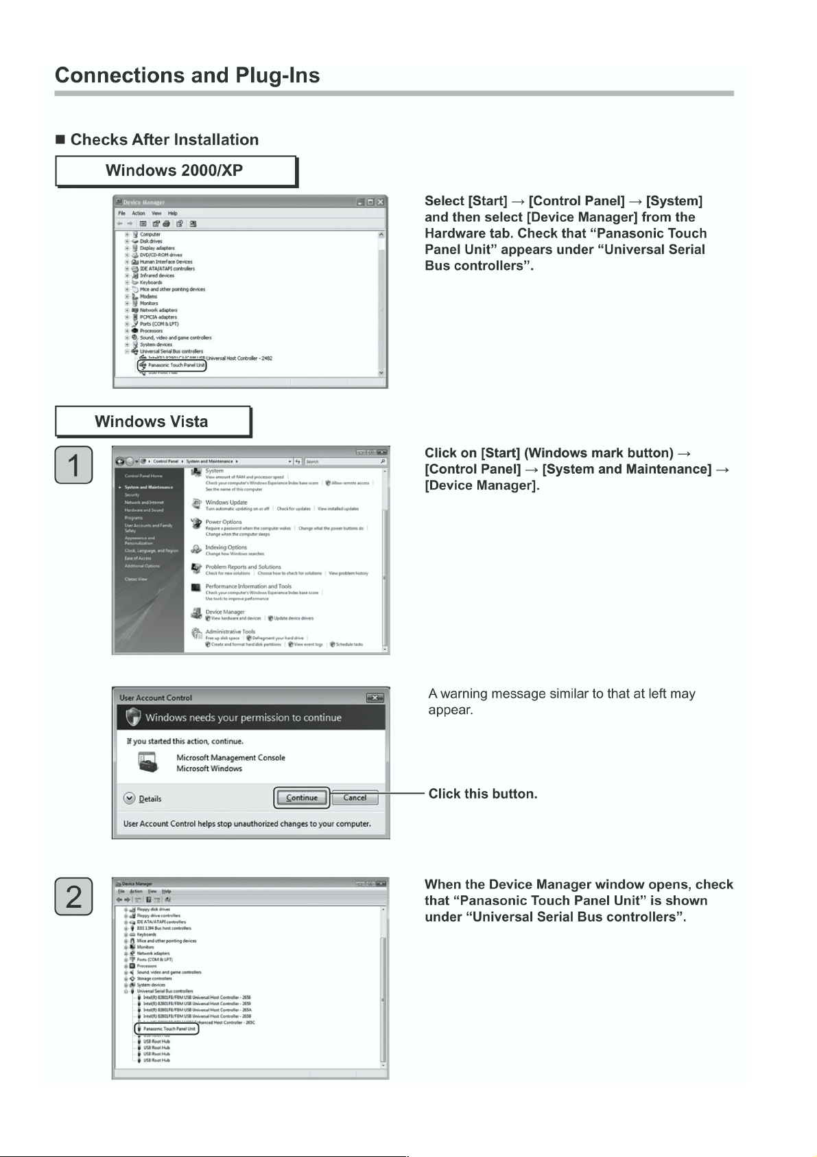
4 Operating Instruc tions
6
789101112131415161718192021222324252627282930313233343536373839


 Loading...