

Panasonic TX-L32S10B, TX-L32S10E, TX-L32S10L, TX-L37S10B, TX-L37S10E Service manual
...
ORDER No. PCZ0903045CE
Service Manual
Colour LCD Television
TX-L32S10B
TX-L32S10E
TX-L32S10L
TX-L37S10B
TX-L37S10E
TX-L37S10L
TX-LF32S10
TX-LF37S10
Specifications
(Informations in brackets [ ] refers to model 32”)
Power Source: 220-240V AC, 50Hz
Power Consumption 130W [115W]
Stand-by Power Consumption: 0.3W (Without monitor out recording)
13W (With monitor out recording)
Aerial Impedance: 75Ω unbalanced, Coaxial Type
Receiving System: S10B S10E,S10L,LFS10
PAL-I PAL-I/H, B/G, D/K
PAL-525/60 (AV only) SECAM B/G, D/K, L/L’
DVB-T (via UHF aerial input) PAL-525/60 (AV only)
M.NTSC (AV only) DVB-T (via VHF/UHF aerial input)
NTSC (AV only) DVB-C (Digital cable services)
M.NTSC (AV only)
NTSC (AV only)
Receiving Channels: S10B S10E,S10L,LFS10
UHF E21-E68 VHF E2-E12 VHF H1-H2 (ITALY)
VHF A-H (ITALY) VHF R1-R2
VHF R3-R5 VHF R6-R12
UHF E21-E69 CATV (S01-S05)
CATV S1-S10 (M1-M10) CATV S11-S20 (U1-U10)
CATV S21-S41 (Hyperband) VHF A-J (IRELAND)
Operating Conditions: Temperature: 0°C ÷ 35°C
Humidity: 20% ÷ 80% RH (non condensing)
PC signals: VGA, SVGA, XGA, SXGA(compressed)
Horizontal scanning frequency 31 – 69 kHz
Vertical scanning frequency 59 – 86 Hz
GLP24 Chassis
© Panasonic Corporation 2008.
Unauthorized copying
distribution is a violation of law.
and

Intermediate Frequency:
Video/Audio S10B S10E,S10L,LFS10
Video 38,9MHz 38,9MHz, 33,9MHz
Audio 32.90MHz 33,4MHz (B/G), 33,16MHz (A2)
32.35MHz(NICAM) 33,05MHz (NICAM B/G, D/K, L’)
32,4MHz (D/K), 32,66MHz (CZ STEREO)
40,4MHz (L’), 39,75MHz (L’ NICAM)
32,90 I, 32.35MHz (NICAM)
Colour 34,47MHz 34,47MHz (PAL)
34,5MHz, 34,65MHz (SECAM)
38,3MHz, 38,15MHz (SECAM L’)
Terminals:
AV1 IN Video (21 pin) 1V p-p 75Ω
Audio (21 pin) 500mV rms 10kΩ
RGB (21 pin) 0,7V p-p 75Ω
AV1 OUT Video (21 pin) 1V p-p 75Ω
Audio (21 pin) 500mV rms 1kΩ
AV2 IN Video (21 pin) 1V p-p 75Ω
Audio (21 pin) 500mV rms 10kΩ
RGB (21 pin) 0,7V p-p 75Ωč
S-video IN (21-pin) Y: 1V p-p 75Ω
C:0,3V p-p 75Ω
AV2 OUT Video (21 pin) 1V p-p 75Ω
Audio (21 pin) 500mV rms 1kΩ
AV3 IN S-Video IN (4-pin) Y: 1V p-p 75Ω
C:0,286V p-p 75Ω
Audio (RCAx2) 500mV rms 10kΩ (used for HDMI3 AUDIO)
Video (RCAx1) 1V p-p 75Ω
HDMI1, HDMI2, HDMI3 Type A Connector
COMPONENT Video (RCAx3) Y:1V p-p 75Ω (including synchronization)
Pb, Pr: ±0,35V p-p 75Ω
AUDIO IN Audio (RCAx2) 500mV rms 10kΩ (used for HDMI1, COMPONENT-AUDIO)
AUDIO OUT Audio (RCAx2) 500mV rms 1kΩ (high Impedance)
DIGITAL AUDIO OUT PCM / Dolby Digital / DTS , Fiber optic
CARD SLOT SD CARD slot ×1
PC HIGH-DENSITY D_SUB 15PIN R,G,B: 700mV p-p 75Ω
HD,VD:TTL Level 2-5V p-p (high impedance)
LCD screen: L5EDD9T00009 [L5EDD8T00004]
1920 x 1080 XGA, 16:9
Visible Diagonal 940mm [800mm]
Audio Output: 20W (2x10W), 10% THD
Headphones: 3,5mm (M3), 8Ω Impedance
Accessories supplied : Remote Control 2 x R6 (UM3) Batteries
Dimensions:
Height: Width: Depth:
Including TV stand 620mm 915mm 287mm
[551mm] [798mm] [217mm]
TV set only 577mm 915mm 97mm
[511mm] [798mm] [93mm]
Net weight:
Including TV stand 16.5kg [13.0kg]
TV set only 14.5kg [11.5kg]
Specifications are subject to change without notice.
Weights and dimensions shown are approximate.
Warning
This service information is designed for experienced repair technicians only and is not designed for use by the general public. It does not
contain warnings or cautions to advise non-technical individuals of potencial dangers in attempting to service a product. Products
powered by electricity should be serviced or repaired only by experienced professional technicians. Any attempt to service or repair the
product or products deal within this service information by anyone else could result in serious injury or death.
2

CONTENTS
SAFETY PRECAUTIONS.......................................................................... 4
GENERAL GUIDE LINES..................................................................... 4
TOUCH – CURRENT CHECK.............................................................. 4
PREVENTION OF ELECTROSTATIC DISCHARGE (ESD)
TO ELECTROSTATICALLY SENSITIVE (ES) DEVICES.......................... 5
ABOUT LEAD FREE SOLDER (PBF)........................................................ 6
SUGGESTED PB FREE SOLDER.......................................................6
APPLICABLE SIGNALS............................................................................. 7
SERVICE HINTS ....................................................................................... 8
CHASSIS BOARD LAYOUT...................................................................... 9
LOCATION OF LEAD WIRING…………………………………………….9
SETTING INSPECTION........................................................................... 10
SELF-CHECK .......................................................................................... 11
POWER LED BLINKING TIMING CHART............................................... 13
SERVICE MODE FUNCTION.................................................................. 14
SERVICE ................................................................................................ 15
OPTION DESCRIPTION.......................................................................... 16
ADJUSTMENT METHOD ........................................................................ 17
WIRING DIAGRAM.................................................................................. 18
BLOCK DIAGRAMS................................................................................. 19
PARTS LOCATION.................................................................................. 22
REPLACEMENT PARTS LIST................................................................. 24
SCHEMATIC DIAGRAMS........................................................................39
A-BOARD (1 OF 18) SCHEMATIC DIAGRAM................................... 40
G-BOARD SCHEMATIC DIAGRAM................................................... 59
V-BOARD SCHEMATIC DIAGRAM ................................................... 60
CONDUCTOR VIEWS............................................................................. 61
3
Safety Precautions
Ω
Ω
General Guide Lines
1. When servicing, observe the original lead dress. If a short circuit is found, replace all parts which have been overhe ated
or damaged by the short circuit.
2. After servicing, see to it that all the protective devices such as insulation barriers, insulation papers shields are properly
installed.
3. After servicing, make the following touch current checks to prevent the customer from being exposed to shock hazards.
4. Always ensure panel TKP0E16001 is correctly replaced before returning to customer (see Fig.1).
Touch-Current Check
1. Plug the AC cord directly into the AC outlet. Do not use an isolation transformer for this check.
2. Connect a measuring network for touch currents between each exposed metallic part on the set and a good earth
ground such as a water pipe, as shown in Fig. 2.
3. Use Leakage Current Tester (Simpson 228 or equivalent) to measure the potential acr oss the measuring network.
4. Check each exposed metallic part, and measure the voltage at each point.
5. Reserve the AC plug in the AC outlet and repeat each of the above measure.
6. The potential at any point (TOUCH CURRENT) expressed as voltage U1 and U2, does not exceed the following values:
For a. c.: U1 = 35 V (peak) and U2 = 0.35 V (peak);
For d. c.: U1 = 1.0 V,
Note:
The limit value of U2 = 0.35 V (peak) for a. c. and U1 = 1.0 V for d. c. correspond to the values 0.7 mA (peak) a. c. and
2.0 mA d. c.
The limit value U1 = 35 V (peak) for a. c. correspond to the value 70 mA (peak) a. c. for frequencies greater than 100
kHz.
7. In case a measurement is out of the limits specified, there is a possibility of a shock hazard, and the equipment shoul d
be repaired and rechecked before it is returned to the customer.
COLD
WATER PIPE
(EARTH GROUND)
TO
APPLIANCES
EXPOSED
METAL PARTS
Resistance values in ohms (Ω)
V: Voltmetr or oscilloscope
(r.m.s. or peak reading)
NOTE – Appropriate measures should be taken to obtain the correct value in case of non-sinusoidal waveforms
Fig. 1
Measuring network for TOUCH CURRENTS
C
R
=1500Ω
S
R0=500Ω
Input resistance: ≥ 1M
Input capacitance: ≤ 200pF
Frequency range: 15Hz to 1MHz and d.c.respectively
Fig. 2
=0.22μF
S
U
10k
1
0.022μF
V
U2 (V)
4

Prevention of Electrostatic Discharge (ESD) to Electrostatically
Sensitive (ES) Devices
Some semiconductor (solid state) devices can be damaged easily by static electricity. Such components commonly are
called Electrostatically Sensitive (ES) Devices. Examples of typical ES devices are integrated circuits and some field-effect
transistors and semiconductor "chip" components. The following techniques should be used to help reduce the incidence of
component damage caused by electrostatic discharge (ESD).
1. Immediately before handling any semiconductor component or semiconductor-equipped assembly, drain off any ESD on
your body by touching a known earth ground. Alternatively, obtain and wear a commercially available discharging ESD
wrist strap, which should be removed for potential shock reasons prior to applying power to the unit under test.
2. After removing an electrical assembly equipped with ES devices, place the assembly on a conductive surface such as
aluminum foil, to prevent electrostatic charge build up or exposure of the assembly.
3. Use only a grounded-tip soldering iron to solder or unsolder ES devices.
4. Use only an anti-static solder removal device. Some solder removal devices not classified as "anti-static (ESD
protected)" can generate electrical charge sufficient to damage ES devices.
5. Do not use freon-propelled chemicals. These can generate electrical charges sufficient to damage ES devices.
6. Do not remove a replacement ES device from its protective package until immediately before you are ready to install it.
(Most replacement ES devices are packaged with leads electrically shorted together by cond uctive foam, aluminum foil
or comparable conductive material).
7. Immediately before removing the protective material from the leads of a replacement ES device, touch the protective
material to the chassis or circuit assembly into which the device will be installed.
Caution
Be sure no power is applied to the chassis or circuit, and observe all other safety precautions.
8. Minimize bodily motions when handling unpackaged replacement ES devices. (Otherwise harmless motion such as th e
brushing together of your clothes fabric or the lifting of your foot from a carpeted floor can generate static electricity
(ESD) sufficient to damage an ES device).
There are special components used in this equipment which are important for safety.
These parts are marked by in schematic diagrams, exploded views and replacement parts list. It is essential that
these critical parts should be replaced with manufacturer’s specified parts to prevent shock, fire, or other hazards. Do
not modify the original design without permission of manufacturer.
IMPORTANT SAFETY NOTICE
5
About lead free solder (PbF)
Note: Lead is listed as (Pb) in the periodic table of elements.
In the information below, Pb will refer to Lead solder, and PbF will refer to Lead Free Solder.
The Lead Free Solder used in our manufacturing process and discussed below is (Sn+Ag+Cu).
That is Tin (Sn), Silver (Ag) and Copper (Cu) although other types are available.
This model uses Pb Free solder in it’s manufacture due to environmental conservation issues. For service and repair work,
we’d suggest the use of Pb free solder as well, although Pb solder may be used.
PCBs manufactured using lead free solder will have the PbF within a leaf Symbol
stamped on the back of PCB.
Caution
• Pb free solder has a higher melting point than standard solder. Typically the melting point is 50 ~ 70 °F (30~40°C)
higher. Please use a high temperature soldering iron and set it to 700 ± 20 °F (370 ± 10 °C).
• Pb free solder will tend to splash when heated too high (a bout 1100 °F or 600 °C).
If you must use Pb solder, please completely remove all of the Pb free solder on the pins or solder area before
applying Pb solder. If this is not practical, be sure to heat the Pb free solder until it melts, before applying Pb solder.
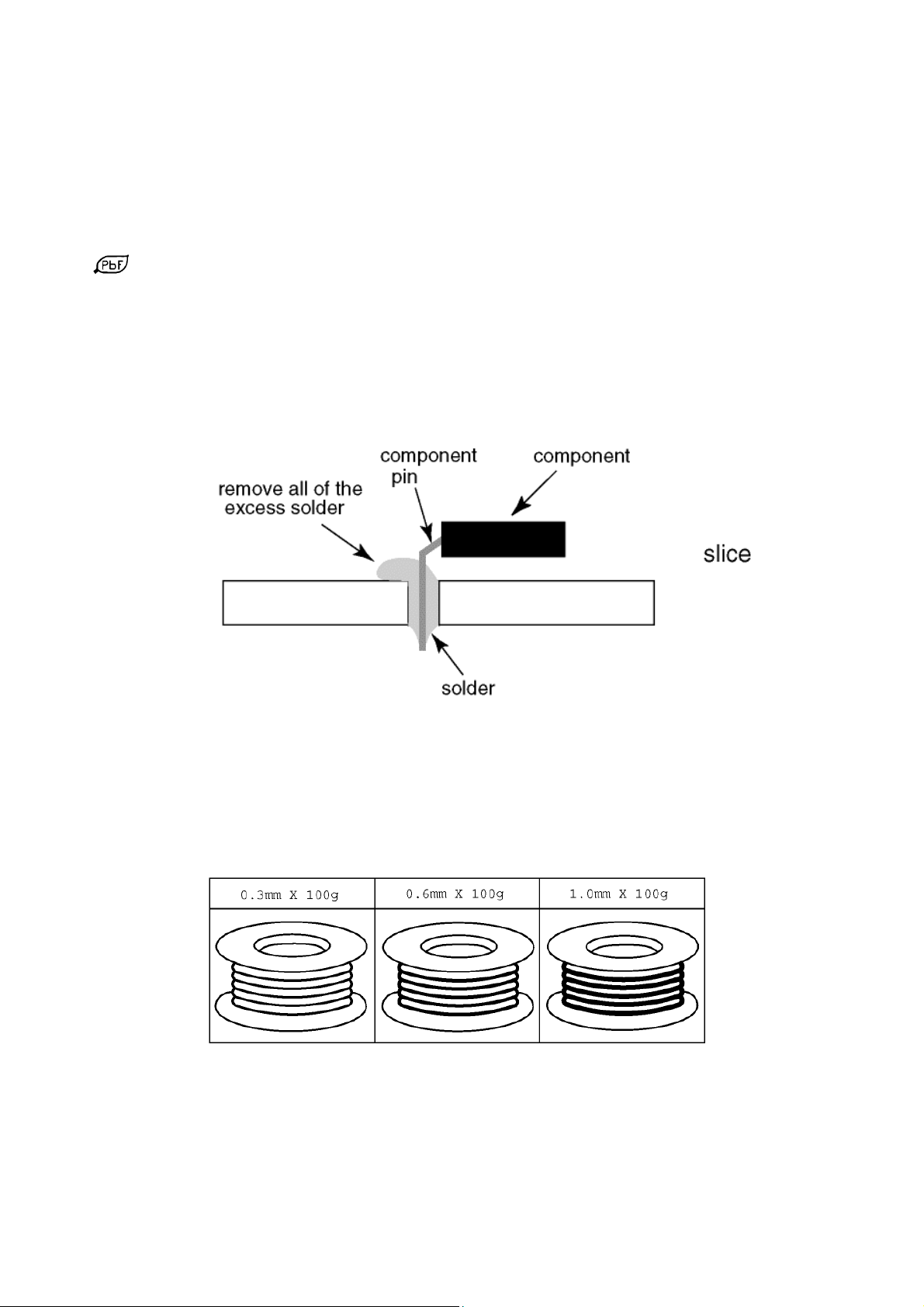
• After applying PbF solder to double layered boards, please check the component side for excess solder which may
flow onto the opposite side. (see Fig.3)
Suggested Pb free solder
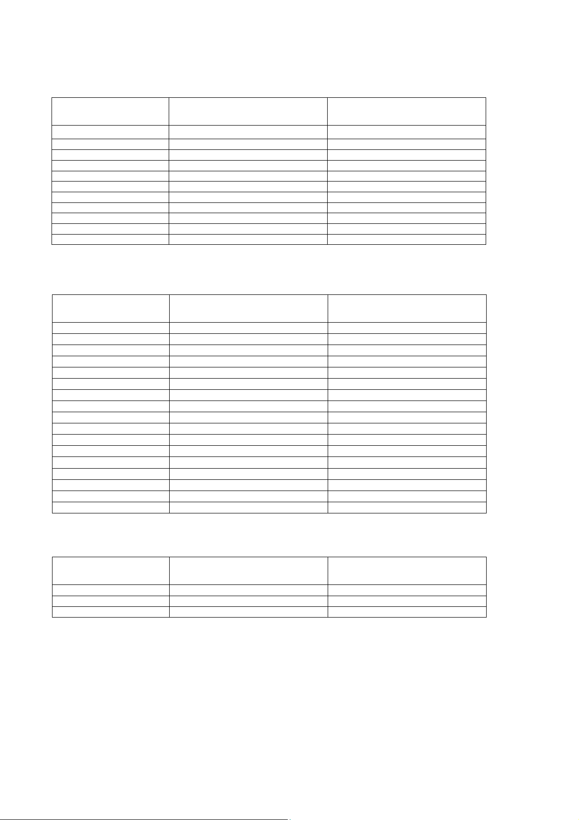
There are several kinds of Pb free solder available for purchase. This product uses Sn+Ag+Cu (tin, silver, copper) solder.
However, Sn+Cu (tin, copper), Sn+Zn+Bi (tin, zinc, bismuth) solder can also be used. (see Fig.4)
Fig.3
Fig.4
6
Applicable Signals
Component (Y, Pb, Pr), HDMI
525 (480) / 60i * *
525 (480) / 60p * *
625 (576) / 50i * *
625 (576) / 50p * *
750 (720) / 60p * *
750 (720) / 50p * *
1,125 (1,080) / 60i * *
1,125 (1,080) / 50i * *
1,125 (1,080) / 60p *
1,125 (1,080) / 50p *
1,125 (1,080) / 24p *
Applicable input signal for PC is basically compatible to VESA standard timing.
Signal name COMPONENT HDMI
PC (from D-sub 15P)
Signal name Horizontal frequency (kHz) Vertical frequency (Hz)
640 × 400 @70 Hz
640 × 480 @60 Hz
640 × 480 @75 Hz
800 × 600 @60 Hz
800 × 600 @75 Hz
800 × 600 @85 Hz
852 × 480 @60Hz
1,024 × 768 @60Hz
1,024 × 768 @70Hz
1,024 × 768 @75Hz
1,024 × 768 @85Hz
1,280 × 768 @60Hz
1,280 × 1,024 @60Hz
1,366 × 768 @60Hz
Macintosh 13“ (640 × 480)
Macintosh 16“ (832 × 624)
Macintosh 21“ (1,152 × 870)
PC (from HDMI terminal)
Applicable input signal for PC is basically compatible to HDMI standard timing.
Signal name Horizontal frequency (kHz) Vertical frequency (Hz)
640 × 480 @60 Hz
750 (720) / 60p 45.00 60.00
1,125 (1,080) / 60p 67.50 60.00
Note:
• Signals other than above may not be displayed properly.
• The above signals are reformatted for optimal viewing on your display.
• PC signal is magnified or compressed for displa y, so that it may not be possible to show fine detail
with sufficient clarity.
31.47 70.07
31.47 59.94
37.50 75.00
37.88 60.32
46.88 75.00
53.67 85.06
31.44 59.89
48.36 60.00
56.48 70.07
60.02 75.03
68.68 85.00
47.70 60.00
63.98 60.02
48.39 60.04
35.00 66.67
49.73 74.55
68.68 75.06
31.47 60.00
7
Service Hints
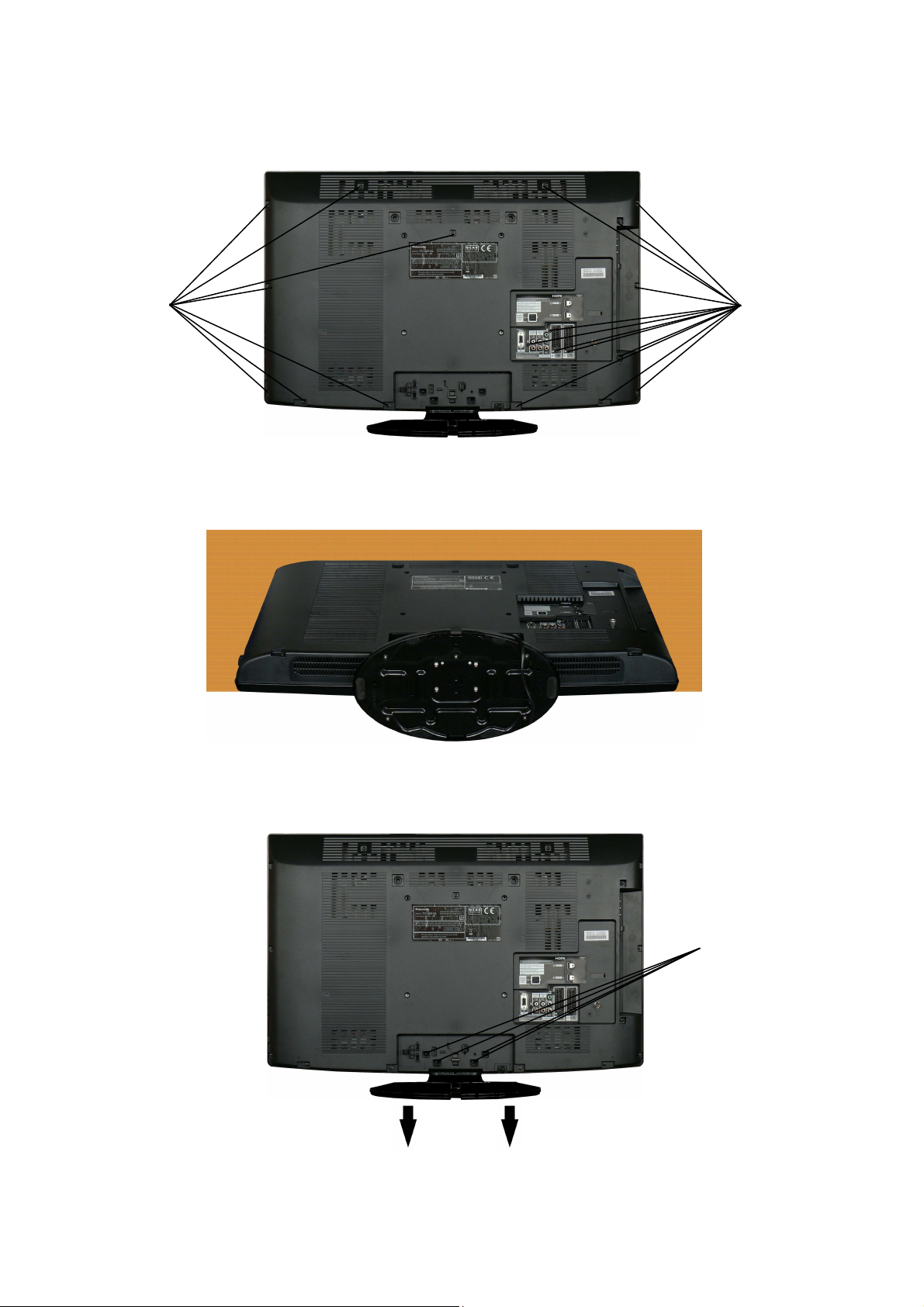
How to remove the backcover
Remove the 19 fixing screws. (see Fig.5)
SCREWS
How to remove the Pedestal assembly
Lay the main unit face down. (see Fig.6)
Remove the 4 fixing screws and the pedestal assembly. (see Fig.7)
Fig.5
Fig.6
Fig.7
SCREWS
SCREWS
8
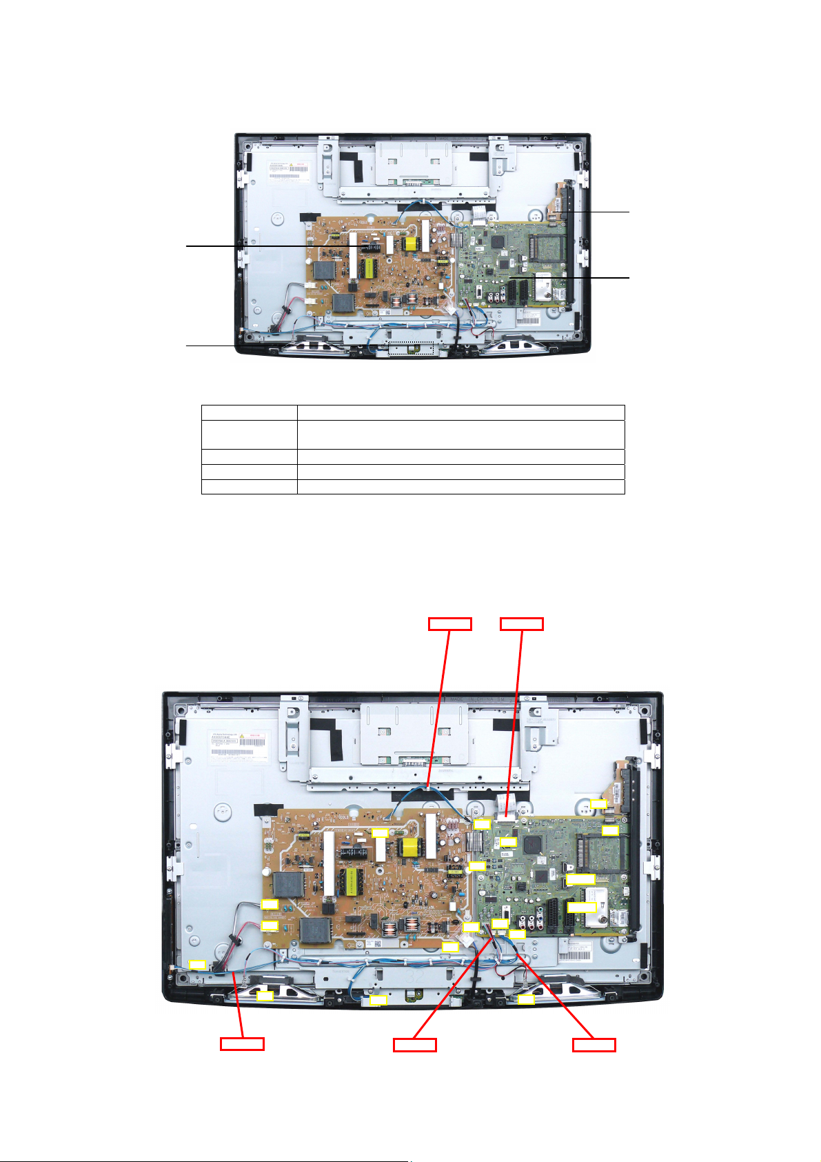
Chassis Board Layout
A11A12A03A01A
A
V
POWER UNIT
V-BOARD
Board Name Function
A-Board Tuner, PC, AVSW,Peaks-AVC,HDMI,CI Slot, Global
Core, GENX, AV Terminal, SD Slot, Speaker out, ADV
Power Unit Power Supply, Main Input
V-Board Remote Receiver, Bats, R/G LED
G-Board Side AV Connector
Location of Lead Wiring
To find the Part Number of required wire in Replacement Parts List click on the wire name in red box.
A11-PAN A20-P4
G-BOARD
A-BOARD
P4
20
G04
A04
S01
P6
P5
P1
10
CN0100
TU2901
SP
10
SP
A01-S01
A12-SP
A10-V10
9

Setting Inspection
Voltage Confirmation
Confirm the following voltages:
A board
5VS TP2765 5.6V +/- 0.25V
SUB_ TNR_6V TP2770 5.6V +/- 0.25V
GND TP2781 0
TV_SOS TP5481 0
INVERTER_SOS TP2761 0
P17V TP2777 17V + / - 1V
SUB_F_12V TP2782 12V +/- 1V
INV_ON TP2759 2,85V +/- 2%
TP No.
Voltage
10
Self Check
Self-check is used to automatically check the bus lines and hexadecimal code of the TV set. To enter Self-Check mode, keep
pressing the down (-/v) button on the TV set and press the STATUS button on the remote control. To exit Self Check,
switch off the TV set at the power button.
TX-L32S10L
TX-L32S10B
TX-L32S10E
TX-L37S10B
TX-L37S10E
32FHD
ADV O.K.
ADAV O.K.
TUN O.K.
GENX O.K.
MEM1 O.K.
MEM2 O.K.
AVSW O.K.
OFDM O.K.
TEMP O.K.
VIF O.K.
32FHD
ADV O.K.
ADAV O.K.
TUN O.K.
GENX O.K.
MEM1 O.K.
MEM2 O.K.
AVSW O.K.
OFDM O.K.
TEMP O.K.
VIF O.K.
32FHD
ADV O.K.
ADAV O.K.
TUN O.K.
GENX O.K.
MEM1 O.K.
MEM2 O.K.
AVSW O.K.
OFDM O.K.
TEMP O.K.
VIF O.K.
37FHD
ADV O.K.
ADAV O.K.
TUN O.K.
GENX O.K.
MEM1 O.K.
MEM2 O.K.
AVSW O.K.
OFDM O.K.
TEMP O.K.
VIF O.K.
37FHD
ADV O.K.
ADAV O.K.
TUN O.K.
GENX O.K.
MEM1 O.K.
MEM2 O.K.
AVSW O.K.
OFDM O.K.
TEMP O.K.
VIF O.K.
Panasonic 2009LCD
Self Check Complete
PEAKS-SOFT 1.206
PEAKS-EEP 01.01.0013
GenX-SOFT 1.00.00
GenX-EEP 1.03.36
GenX-ROMCORR 1.00.00
Panasonic 2009LCD
Self Check Complete
PEAKS-SOFT 1.206
PEAKS-EEP 01.00.0017
GenX-SOFT 1.00.00
GenX-EEP 1.03.36
GenX-ROMCORR 1.00.00
Panasonic 2009LCD
Self Check Complete
PEAKS-SOFT 1.206
PEAKS-EEP 01.00.0003
GenX-SOFT 1.00.00
GenX-EEP 1.03.36
GenX-ROMCORR 1.00.00
Panasonic 2009LCD
Self Check Complete
PEAKS-SOFT 1.206
PEAKS-EEP 01.00.0016
GenX-SOFT 1.00.00
GenX-EEP 1.03.36
GenX-ROMCORR 1.00.00
Panasonic 2009LCD
Self Check Complete
PEAKS-SOFT 1.206
PEAKS-EEP 01.00.0002
GenX-SOFT 1.00.00
GenX-EEP 1.03.36
GenX-ROMCORR 1.00.00
11
SUM
MODEL ID
EDID
SUM
MODEL ID
EDID
SUM
MODEL ID
EDID
SUM
MODEL ID
EDID
SUM
MODEL ID
EDID
7997
06
030b3100
00000004
22 1b0bfb--
7993
06
03043100
00000004
22 1b0bfb--
798D
06
03113100
00000004
22 1b0bfb--
7992
06
03043100
00000010
22 1b0bfb--
798C
06
03113100
00000010
22 1b0bfb--
TX-L37S10L
TX-LF32S10
TX-LF37S10
37FHD
ADV O.K.
ADAV O.K.
TUN O.K.
GENX O.K.
MEM1 O.K.
MEM2 O.K.
AVSW O.K.
OFDM O.K.
TEMP O.K.
VIF O.K.
32FHD
ADV O.K.
ADAV O.K.
TUN O.K.
GENX O.K.
MEM1 O.K.
MEM2 O.K.
AVSW O.K.
OFDM O.K.
TEMP O.K.
VIF O.K.
37FHD
ADV O.K.
ADAV O.K.
TUN O.K.
GENX O.K.
MEM1 O.K.
MEM2 O.K.
AVSW O.K.
OFDM O.K.
TEMP O.K.
VIF O.K.
Panasonic 2009LCD
Self Check Complete
PEAKS-SOFT 1.206
PEAKS-EEP 01.01.0012
GenX-SOFT 1.00.00
GenX-EEP 1.03.36
GenX-ROMCORR 1.00.00
anasonic 2009LCD
Self Check Complete
PEAKS-SOFT 1.206
PEAKS-EEP 01.00.0003
GenX-SOFT 1.00.00
GenX-EEP 1.03.36
GenX-ROMCORR 1.00.00
Panasonic 2009LCD
Self Check Complete
PEAKS-SOFT 1.206
PEAKS-EEP 01.01.0002
GenX-SOFT 1.00.00
GenX-EEP 1.03.36
GenX-ROMCORR 1.00.00
SUM
MODEL ID
EDID
SUM
MODEL ID
EDID
SUM
MODEL ID
EDID
7996
06
030B3100
00000010
22 1b0bfb--
798D
06
031C3100
00000004
22 1b0bfb--
798C
06
031C3100
00000010
22 1b0bfb--
Display Ref. No. Description P.C.B.
ADV IC4510 A/D CONVERTER A-Board
ADAV IC4510 A/D CONVERTER A-Board
TUN TU2901 TUNER A-Board
GENX IC1100 MICROPROCESSOR A-Board
MEM1 IC1101 EEPROM (GENX) A-Board
MEM2 IC8601 EEPROM (PEAKS AVC) A-Board
AVSW IC3001 AUDIO VIDEO SWITCH A-Board
COFDM IC8301 COFDM DEMODULATOR A-Board
TEMP IC2750 TEMP SENSOR A-Board
VIF TU2901 TUNER A-Board
If the CCU ports have been checked and found to be incorrect or not located then " - - " will appear in place of "O.K.".
12
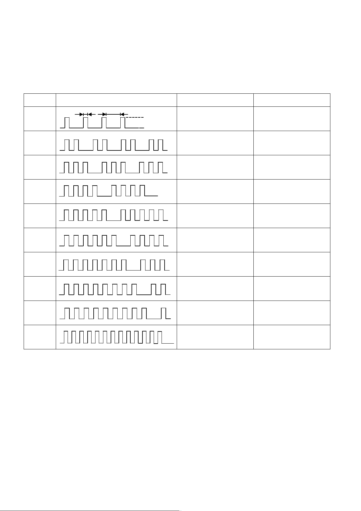
Power LED blinking timing chart
1. Subject
Information of LED Flashing timing chart.
2. Contents
When abnormality has occurred the unit, the protection circuit operates and reset to the stand by mode. At this time, the
defective block can be identified by number of blinking of the Power LED on the front panel of the unit.
Blinking
times
Once
1 INVERTER_SOS
2 FAN_SOS A BOARD
3 SOS
4
Blinking timing Contents Check point
4 sec
Light
No Light
LCD PANEL
A BOARD
A BOARD
SUB_F_12V A BOARD
5 MAIN9V A BOARD
6 SUB5V
7 SUB3.3V A BOARD
8 MAIN3.3V A BOARD
9 SOUND_SOS A BOARD
13 EMERGENCY SOS A BOARD
A BOARD
V BOARD
13

Service Mode Function
MPU controls the functions switching for each IICs through IIC bus in this chassis. The following setting and adjustment can be
adjusted by remote control in Service Menu
How to enter SERVICE
While pressing (-/v) button on TV unit, press on the remote
control for 3 times within 2 seconds.
Note:
To exit from Service mode, press the exit button on remote control.
0
14

SERVICE
A
A
A
A
A
SERVICE
ADJUST
WB-ADJ
OPTION
SRV-TOOL
Peaks SOFT 1.206 OPTION 1 1c
Peaks EEP 01.00.0013 OPTION 2 ef
LSI DATA 0.00.00 OPTION 3 01
STBY SOFT 1.00.00 Model ID 06
STBY EEP 1.03.36 030b3100
STBY ROMCOR 1.00.00 00000004
RB Cnt 000
INV Cnt 0000
1
ADJUST DYNAMIC
CONTRAST
YMAX
1,2:MAIN SELECT
3,4:SUB SELECT
9 :PICTURE MENU SELECT
YELLOW:AUTO ADJUST
VOL:ADJUST
OK :WRITE
1
WB-ADJ DYNAMIC
R-GAIN
COLOR TEMP NORMAL
1,2:MAIN SELECT
3,4:SUB SELECT
7 :COLOR TEMP SELECT
9 :PICTURE MENU SELECT
VOL:ADJUST
OK :WRITE
1
OPTION DYNAMIC
Boot
1,2:MAIN SELECT
3,4:SUB SELECT
9 :PICTURE MENU SELECT
VOL:ADJUST
1
SRV-TOOL DYNAMIC
000
FF
ROM
00
2
ADJUST DYNAMIC
3
COLOR
1,2:MAIN SELECT
4
3,4:SUB SELECT
9 :PICTURE MENU SELECT
VOL:ADJUST
OK :WRITE
2
WB-ADJ DYNAMIC
G-GAIN
3
COLOR TEMP NORMAL
1,2:MAIN SELECT
3,4:SUB SELECT
4
7 :COLOR TEMP SELECT
9 :PICTURE MENU SELECT
VOL:ADJUST
OK :WRITE
2
OPTION DYNAMIC
STBY-SET
3
1,2:MAIN SELECT
4
3,4:SUB SELECT
9 :PICTURE MENU SELECT
OK :POWER OFF
2
3A
FF
00
DJUST DYNAMIC
3
TINT
1,2:MAIN SELECT
4
3,4:SUB SELECT
9 :PICTURE MENU SELECT
VOL:ADJUST
OK :WRITE
WB-ADJ DYNAMIC
B-GAIN
3
COLOR TEMP NORMAL
1,2:MAIN SELECT
3,4:SUB SELECT
4
7 :COLOR TEMP SELECT
9 :PICTURE MENU SELECT
VOL:ADJUST
OK :WRITE
OPTION DYNAMIC
Emergency
3
1,2:MAIN SELECT
4
3,4:SUB SELECT
9 :PICTURE MENU SELECT
VOL:ADJUST
Key Command
• Press the 3/4 button to change the adjustment values or function.
• Press the 1/2 button to step up/down through the functions and adjustments
• Press the numerical button VOLUME (+/-) to change option item.
• Press the OK button after each adjustment has been made to store the required values.
ON
00
E6
ADJUST DYNAMIC
3
SUB-BRT
1,2:MAIN SELECT
4
3,4:SUB SELECT
9 :PICTURE MENU SELECT
VOL:ADJUST
OK :WRITE
WB-ADJ DYNAMIC
R-CENT
3
COLOR TEMP NORMAL
1,2:MAIN SELECT
3,4:SUB SELECT
4
7 :COLOR TEMP SELECT
9 :PICTURE MENU SELECT
VOL:ADJUST
OK :WRITE
OPTION DYNAMIC
Y/C Delay
3
1,2:MAIN SELECT
4
3,4:SUB SELECT
9 :PICTURE MENU SELECT
VOL:ADJUST
OK :WRITE
800
7F
DJUST DYNAMIC
3
BACKLIGHT
1,2:MAIN SELECT
4
3,4:SUB SELECT
9 :PICTURE MENU SELECT
VOL:ADJUST
OK :WRITE
WB-ADJ DYNAMIC
G-CENT
3
COLOR TEMP NORMAL
1,2:MAIN SELECT
3,4:SUB SELECT
7 :COLOR TEMP SELECT
9 :PICTURE MENU SELECT
VOL:ADJUST
OK :WRITE
OPTION DYNAMIC
OPT 1
3
1,2:MAIN SELECT
4
3,4:SUB SELECT
5,6:BIT SELECT
9 :PICTURE MENU SELECT
VOL:ADJUST
OK :WRITE
4E6
80
00011100
DJUST DYNAMIC
H-POS
3
1,2:MAIN SELECT
4
3,4:SUB SELECT
9 :PICTURE MENU SELECT
VOL:ADJUST
OK :WRITE
WB-ADJ DYNAMIC
B-CENT
3
COLOR TEMP NORMAL
1,2:MAIN SELECT
3,4:SUB SELECT
4 4
7 :COLOR TEMP SELECT
9 :PICTURE MENU SELECT
VOL:ADJUST
OK :WRITE
OPTION DYNAMIC
OPT 2
3
1,2:MAIN SELECT
4
3,4:SUB SELECT
5,6:BIT SELECT
9 :PICTURE MENU SELECT
VOL:ADJUST
OK :WRITE
11101111
7B
DJUST DYNAMIC
0
H-AMP
3
1,2:MAIN SELECT
4
3,4:SUB SELECT
9 :PICTURE MENU SELECT
VOL:ADJUST
OK :WRITE
OPTION DYNAMIC
OPT 3
3
1,2:MAIN SELECT
4
3,4:SUB SELECT
5,6:BIT SELECT
9 :PICTURE MENU SELECT
VOL:ADJUST
OK :WRITE
0
00000001
ADJUST DYNAMIC
V-POS
3
1,2:MAIN SELECT
4
3,4:SUB SELECT
9 :PICTURE MENU SELECT
VOL:ADJUST
OK :WRITE
DJUST DYNAMIC
0
V-AMP
3
1,2:MAIN SELECT
4
3,4:SUB SELECT
9 :PICTURE MENU SELECT
VOL:ADJUST
OK :WRITE
0
1,2:MAIN SELECT
9 :PICTURE MENU SELECT
OK :ENTER
15
Option Bytes Description
OPTION1
b0 ATP Search Speed Slow (1) / Fast (0)
b1 TXT Ch Refresh On (1) / Off (0)
b2 ID-1 On (1) / Off (0)
b3 Macrovision Auto-Judge On (1) / Off (0)
b4 Surround enable low bit (*1) On (1) / Off (0)
b5 Surround enable low bit (*1) On (1) / Off (0)
b6 Pre Emphasis On (1) / Off (0)
b7 TINT_COMPONENT_HDMI On (1) / Off (0)
OPTION2
b0 Adjust lgain enable On (1) / Off (0)
b1 A2 BC enable (5.5) On (1) / Off (0)
b2 A2 DK1 enable (6.26) On (1) / Off (0)
b3 A2 DK3 enable (5.742) On (1) / Off (0)
b4 NICAM scan On (1) / Off (0)
b5 NICAM enable (5.5) On (1) / Off (0)
b6 NICAM enable (6.0) On (1) / Off (0)
b7 NICAM enable (6.5) On (1) / Off (0)
OPTION3
b0 NICAM priority (ASIA/M.E) On (1) / Off (0)
b1 NICAM priority (K/UK) On (1) / Off (0)
b2 NICAM priority (China) On (1) / Off (0)
b3 NICAM priority (NZ/INDN) On (1) / Off (0)
b4 NICAM priority (AUS) On (1) / Off (0)
b5 NICAM priority (E.Europe) On (1) / Off (0)
b6 NICAM priority (Special) On (1) / Off (0)
b7 SASO mute Not use
OPTION4
b0 All country DVB-S enable On (1) / Off (0)
b1 All country DVB-C enable On (1) / Off (0)
16

Adjustment Method
Sub-Contrast/White Balance Adjustment
Instrument Name Connect to Remarks
1. Remote controller
2. LCD WB meter (Minolta CS-1000A equivalent)
3. Comunication jig
4. Computer for external control
Procedure Remarks
Subcontrast adjustment
1. Receive PAL colour bar (100% white) RF signal.
2. Enter “Contrast” adj. In SERVICE mode.
3. Start adjusting by using Yellow Key.
4. If the adjustment finished normally, the letter of Contrast will change from red
to black
White Balance adjustment
1. Procedure basically performs checking using the production software and
make automatic adjustment using external computer.
2. It adjusts in the mode of : Colour balance Normal as follows.
Viewing Mode Dynamic
S10B/L S10E,LFS10
WHITE Normal WHITE Normal
x: 0,2860 ± 0,010 x: 0,2820 ± 0,010
y: 0,3130 ± 0,010 y: 0,3020 ± 0,010
GRAY Normal GRAY Normal
x: 0,2840 ± 0,010 x: 0,2840 ± 0,010
y: 0,3140 ± 0,010 y: 0,3120 ± 0,010
Correlation can be also taken by
CA-210 or equivalent
Let the panel standfor more than 3
hours at more than 20 °C.
Basically perform adjustment in the
ambient environment of room
temperature more than 20 °C.
The aging time is more than20 min
at above room temperature.
Applied signal
100% full colour bar
0,7V p-p white peak
87.5% modulation
100% WHITE
50% GRAY
17
Wiring Diagram
LCD PANEL
HDMI 3
HDMI 1
JK4501 JK4502
HDMI 2
JK4500
JK8401
CI SLOT
YPBPR
JK3100
SD CARD
JK8302
SERVICE
CN0100
TUNER
TU2901
A-BOARD
MAIN INPUT
A11
A20
A03
A10
P6
P4
P2
V10
P5
P1
POWER UNIT
V-BOARD
PC
KEY
SP L/R
JK3001
A01
A12
JK3002
AV1
JK3003
AV2
D3015
OPT
A04
18
G04
G-BOARD
JK3700
AV3
Video & Stereo Audio Block Diagram
IC3001
AV-SWITCH
[C1AB00002855]
AV1_V 20
AV1_VOUT 19
AV1_RED 15
AV1_GREEN 11
AV1_BLUE 7
JK3002
JK3003
Y,PB,PR
AUDIO IN/OUT,
PC INPUT
AV1_L 6
AV1_LOUT 3
AV1_R 2
AV1 21PIN SCART
AV1_ROUT 1
AV2_V 20
AV2_VOUT 19
AV2_RED/C 15
AV2_GREEN 11
AV2_BLUE 7
AV2_L 6
AV2_LOUT 3
AV2_R 2
AV2 21PIN SCART
AV2_ROUT 1
Y
PB
PR
L
R
JK3100
L
R
1
2
3
JK3001
Y
PB
PR
PC L IN
PC R IN
RCA AUDIOOUT L
RCA AUDIOOUT R
PC R
PC G
PC B
79 CVBS IN6
44 CVBS/Y+C OUT
43 SAGCVBS OUT3
91 R3
89 G3
87 B3
62 L3IN
56 L1OUT
63 R3IN
55 R1OUT
19 G1/Y IN
23 CVBS IN2
38 Y/Y+CVBSOUT4
37 SAGCVBSOUT4
11 R2/C IN
21 B1/C IN
13 G2/Y IN
15 B2/ C IN
64 L4 IN
54 L4 OUT
65 R IN
53 R2 OUT
95 CY IN1
93 PB IN1
97 PR IN1
70 L IN
71 R IN
52 L OUT
51 R OUT
3 R IN
1 G IN
99 B IN
R6 IN
69 L6 IN
68
AV4 R
AV4 L
AV4 V
83 Y IN4
81 CVBS IN5
AV4 Y
85 C IN4
AV4 C
CVBSin4 5
AV R 49
AV L 50
TV R 60
TV L 61
AUDIOOUT R 59
AUDIOOUT L 58
CVBSin 17
31
33
35
46
DVB CVBS
MAIN Y/CVBS
MAIN PB/C
MAIN PR
RGB CVBS
AV R
AV L
TV R
TV L
AUDIOOUT R
AUDIOOUT L
HP L
HP R
OPT_SPDIF
SOY
MAIN RF SIGNAL CVBS
A14
A12
A13
B10
A15
A21
B21
C22
C23
D22
D23
M20 SPDIF_OUT
H22 HPOUT1L
H23 HPOUT1R
IC4510
ADV
[C1AB00003045]
AUDIO VIDEO DECODER
DIGITAL VIDEO OUT
N23
PWM WO L+
5
IC2301
[C1AB00002875]
MAIN AUDIO AMPLIFIER
SP L-
SP L+
N22
M23
PWM WO R+
PWM WO L-
12
7
253034
SP R+
SIF IN2
A17
SIF IN1
A18
AUX INL
B22
AUX INR
A22
M22
PWM WO R14
21
SP R-
RX
RX
RX
8
8
8
DVB CVBS
DDR2 800MHz
IC8002
IC8003
HDMI1
HDMI3
HDMI2
D12
E25,B25,C25,D25
FL4201
FL4203
F25,E26,B26
C26,D26,F26,
FL4202
IC8580
[TVRQ370AE]
NOR FLASH
IC8001- AVC
[MN2WS0059]
IIC 3
IIC
IC1100
GenX8
[MNZSFH9GP8L]
IC8301
[C1AB00003049]
TS SERIAL
BUS I/F
SD CARD I/F
57
58
2
SD CARD DATA
IC1101
[C3EBFC000042]
EEPROM GenX8
JK4501 JK4500
HDMI1HDMI2
MAIN RF SIGNAL CVBS
SIF
AM
IFD1
IFD2
IFAGC
JK4502
HDMI3
TUNER
TU2901
ENG37E18KF
21
11
10
12
17
19
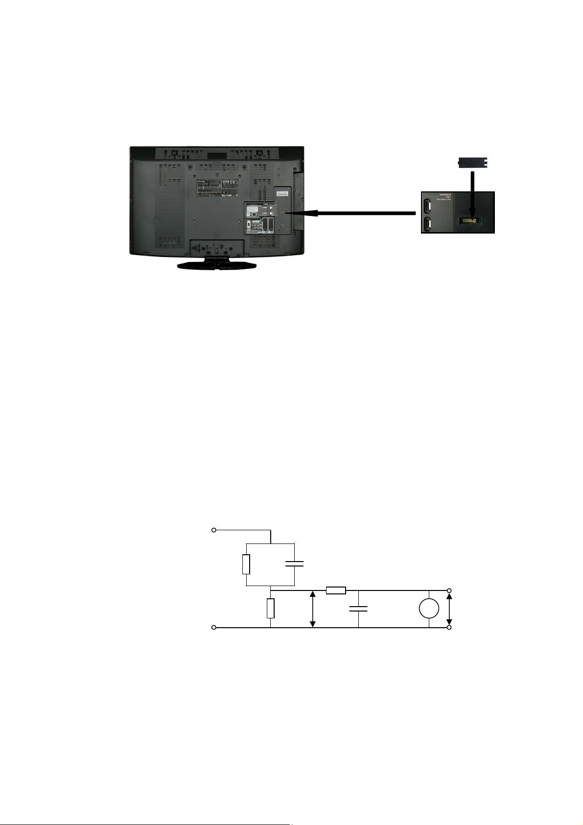
CI SLOT
CI SLOT
JK8401
JK8401
SD SLOT
JK8302
HDMI TERMINAL
RX0-
RX0+
RX1-
RX1+
RX2-
RX2+
RXCLK-
RXCLK+
RX3-
RX3+
2 4 6 8 10 3 1
A04
OPT
D3015
1 2 3 4
A12
20 19 17 16 14 13 11 10 8 7
A11
DIGITAL AUDIO OUT
R
L
V
JK3700
G-BOARD
Y
C
L
R
AV4 R
AV4 L
AV4 V
AV4 Y
AV4 C
HP L OUT
HP R OUT
2 4 6 8 10 3 1
G04
L-
L+
SP L
R-
R+
SP R
LCD PANEL
19
 Loading...