

Panasonic DMRHS-2 Service manual
Table Of Contents
COVER
1 COMPARISON CHART
1.1 Comparison for each part
1.2 Comparison for function
2 SAFETY PRECAUTIONS
2.1 GENERAL GUIDELINES
2.1.1 LEAKAGE CURRENT COLD
CHECK
2.1.2 LEAKAGE CURRENT HOT
CHECK (See Figure 1 .)
3 PREVENTION OF ELECTRO
STATIC DISCHARGE (ESD) TO
ELECTROSTATICALLY SENSITIVE
(ES) DEVICES
4 Precaution of Laser Diode
5 How to replace the Lithium Battery
6 Handling the Lead-free Solder
6.1 About lead free solder (PbF)
7 General Description
7.1 Control reference guide
7.2 PC CARD (JPEG)
7.3 Still pictures (JPEG)
7.4 Checking the Accessories
8 Notes When Servicing the Unit
8.1 When the disc of a customer
cannot be pulled out due to a failure
8.2 When the ratings password is
forgotten
8.3 When the disc cannot be taken out
due to sales demonstration lock function
8.4 Handling of HDD
9 Assembling and Disassembling
9.1 Disassembly flow chart
9.2 P.C.B. positions
9.3 The Top cover
9.4 The Front panel
9.5 The PC Card P.C.B.
9.6 The Digital P.C.B.
9.7 The ATAPI P.C.B.
9.8 The Front (L)/(R)
P.C.B.,Stick P.C.B. and DV Jack P.C.B.
9.9 The DVD-RAM drive
9.10 The Rear panel
9.11 The HDD
9.12 The Power supply P.C.B.
9.13 The Main P.C.B.
9.14 Scart P.C.B.
9.15 RGB P.C.B.
9.16 The VIF Decoder P.C.B. and
Nicam/Decoder P.C.B.
10 Service Positions and Tools
10.1 Checking procedure
10.2 Checking PC card P.C.B.
10.3 Checking the Power supply
P.C.B. and the DVD-RAM drive
10.4 Checking the Power supply and
Main P.C.B.s
10.5 Service tools
11 Repair and checking procedures
11.1 Flow chart
11.2 Inspection and checking
Service Manual
TOP NEXT
ORDER NO.ODSD020948C8
DVD Video Recorder
● DMR-HS2EB
DMR-HS2EB1
DMR-HS2EG
DMR-HS2EG1
DMR-HS2GN
Colour
(S).......................Silver Type
Specifications
Power supply: AC220-240 V, 50 Hz
Power consumption: 39 W
Recording system: DVD video recording standards (DVD-RAM),
DVD video standards (DVD-R)
Hard disk drive capacity: 40 GB
Recordable discs: 12 cm 4.7 GB DVD-RAM
12 cm 9.4 GB DVD-RAM
8 cm 2.8 GB DVD-RAM
12 cm 4.7 GB DVD-R
(for General Ver. 2.0)
Recording time: Max. 6 hours
(using 4.7 GB disc)
XP: Approx. 1 hour
SP: Approx. 2 hours
LP: Approx. 4 hours
EP: Approx. 6 hours
Max. 52 hours
(using Hard disc drive)
XP:Approx. 8.5 hours
SP: Approx. 17 hours
LP: Approx. 34 hours
EP: Approx. 52 hours
Region Number: Region No.2 (HS2EB/ EB1/ EG/ EG1)
Region No.4 (HS2GN)
Playable discs: 12 cm 4.7 GB DVD-RAM
12 cm 9.4 GB DVD-RAM
8 cm 2.8 GB DVD-RAM
12 cm 4.7 GB DVD-R
(for General Ver. 2.0)
DVD-Video
CD-Audio (CD-DA)
Video CD
CD-R/RW
(CD-DA,Video CD formatted discs)
Audio
Recording system: Dolby Digital, 2ch
LINEAR PCM
(for XP mode only, selectable)
Audio In: AV1/AV2 (21 pin) AV3/AV4 (pin jack)
Input Level: Standard: 0.5 Vms
Full scale: 2 Vms at 1k Hz

procedures
11.3 Hint for repair
11.4 Special modes at a glance
12 Abbreviations
13 Voltage Chart
13.1 Power Supply P.C.B.
13.2 Main P.C.B.
13.3 RGB P.C.B.
13.4 Scart P.C.B.
13.5 Nicam/Decoder P.C.B.
13.6 P9001 Connector
13.7 P9001 Waveform
14 Block Diagram
14.1 Power Supply Block Diagram
14.1.1 Integrated Circuit Power
Supply Chart
14.2 Analog Audio Block Diagram
14.3 Analog Video Block Diagram
14.4 Analog Timer Block Diagram
14.5 Digital Section Block Diagram
14.5.1 Digital Section Block Diagram
(1)
14.5.2 Digital Section Block Diagram
(2)
14.5.3 Digital Block IC Pin Terminal
Chart (TC1-TC28)
15 Schematic Diagram
15.1 Interconnection Schematic
Diagram
15.2 Power Supply Schematic
Diagram (Power Supply P.C.B.
(1/2))
15.3 Power Supply Schematic
Diagram (Power Supply P.C.B.
(2/2))
15.4 Main Net Section (Main P.C.B.
(1/4)) Schematic Diagram (M)
15.5 Video I/O Section (Main
P.C.B. (2/4)) Schematic Diagram
(V)
15.6 Audio Main Section (Main
P.C.B. (3/4)) Schematic Diagram
(A)
15.7 Timer Section (Main P.C.B.
(4/4)) Schematic Diagram (T)
15.8 Digital Net Section (Digital
P.C.B. (1/7)) Schematic Diagram
(DN)
15.9 AV-Encoder Section (Digital
P.C.B. (2/7)) Schematic Diagram
(EN)
15.10 AV-Decoder Section (Digital
P.C.B. (3/7)) Schematic Diagram
(AD)
15.11 AV-Input Section (Digital
P.C.B. (4/7)) Schematic Diagram
(AI)
15.12 System Control Section (Digital
P.C.B. (5/7)) Schematic Diagram
(S)
15.13 Glue Section (Digital P.C.B.
(6/7)) Schematic Diagram (G)
15.14 1394 D/V Section (Digital
P.C.B. (7/7)) Schematic Diagram
Input Impedance: more than 10k ohm
Audio Out: AV1/AV2 (21 pin) Audio Out (pin jack)
Output Level: Standard: 0.5 Vms
Full scale: 2Vms at 1k Hz
Output Impedance: less than 1k ohm
Digital Audio Out: Optical terminal (PCM, Dolby Digital, DTS, MPEG)
Television System
Tuner System: PAL I 75 ohm
Channel Coverage:
DMR-HS2EB/EB1 only UHF: CH 21-68
DMR-HS2EG/EG1 only VHF: CH E2-E12, A-H2 (For Italy)
UHF: CH 21-69
CATV: CH S01-S05 (S1-S3)
S1-S20 (M1-U10)
S21-S41 [8MHz, RASTER]
DMR-HS2GN VHF: CH 0-12
(For Australia) UHF: CH 28-69
CATV: 45MHz-470MHz
DMR-HS2GN VHF: CH 1-11
(For New Zealand) UHF: CH 21-69
CATV: 44MHz-470MHz
RF Converter Output: UHF: CH21-68, 75 ohm
(For the United kingdom)
Not provided
(Except the United kingdom)
Video
Video System: PAL colour signal, 625 lines, 50 fields
NTSC colour signal, 525 lines, 60 fields
Recoeding system: MPEG2 (Hybrid VBR)
Video in: AV1/AV2 (21 pin), AV3/AV4 (pin jack)
1Vp-p 75 ohm, terminated
S-Video in: AV2 (21 pin), AV3/AV4 (S terminal)
1Vp-p 75 ohm, terminated
RGB In: AV2 (21 pin), 0.7Vp-p (PAL) 75 ohm, terminated
Video Out: AV1/AV2 (21 pin), Video Out (pin jack)
1Vp-p 75 ohm, terminated
S-Video Out: AV1 (21 pin), S-Video Out(S terminal)
1Vp-p 75 ohm, terminated
RGB Out: AV1 (21 pin) 0.7Vp-p (PAL) 75 ohm, terminated
Dimensions(W)x(H)x(D): Approx. 430x79x306 mm
Mass: Approx. 4.5 Kg
Operating Temperature: 5°C-40°C
Operating Humidity range: 10%-80% RH (no condensation)
LEASER Specification
Class 1 LASER Product
Wave Length: 775-815nm, 655-666nm
Laser Power: No hazardous radiation is emitted with the safety protection
DV Input: 4 pin
PC card slot: PC Card Type II
Compatible media: A PC Card adaptor conforming to PC Card Standards
PC Card adaptor (SD Memory Card, Multi Media Card, Compact Flash, Smart Media, Memory Stick)
Format: FAT12 or FAT16
Image format: JPEG conforming to DCF (Design Rules for Camera Files System universal standard)
DPOF Compatible
Number of pixels: 320×240 to 6144×4096
(sub sampling; 4:2:2 or 4:2:0)
Thawing time: Approx. 7 sec. (2 M pixels)
Notes:
Mass and dimensions shown are approximate.
Specifications are subject to change without notice.
Notes:
The part of DVD RAM Drive (VXY1748) is listed separately.
Please refer to ORDER NO. DSD0207004C0.
© 2002 Matsushita Electric Industrial CO., Ltd. All rights reserved. Unauthorized copying and distribution is a violation of law.
(DV)
15.15 PC Card Schematic Diagram
15.16 ATAPI Schematic Diagram
15.17 RGB Schematic Diagram
15.18 Scart Schematic Diagram
15.19 VIF Decoder Schematic
Diagram
15.20 Nicam/Decoder Schematic
Diagram
15.21 Front (R) Schematic Diagram
15.22 Front (L) Schematic Diagram
15.23 DV Input Jack Schematic
Diagram
15.24 Stick Schematic Diagram
16 Print Circuit Board
16.1 Power Supply P.C.B.
16.2 Main P.C.B. Location Map,
Address Information
16.2.1 Main P.C.B. Location Map
16.2.2 Main P.C.B. Address
Information
16.3 Main P.C.B.
16.3.1 Main P.C.B. (1/4 Section)
16.3.2 Main P.C.B. (2/4 Section)
16.3.3 Main P.C.B. (3/4 Section)
16.3.4 Main P.C.B. (4/4 Section)
16.4 Digital P.C.B. Location Map,
Address Information
16.4.1 Digital P.C.B. (Component
Side) Location Map
16.4.2 Digital P.C.B. (Foil Side)
Location Map
16.4.3 Digital P.C.B. Address
Information
16.5 Digital P.C.B. (Component Side)
16.5.1 Digital P.C.B. (Component
Side) 1/2 Section
16.5.2 Digital P.C.B. (Component
Side) 2/2 Section
16.6 Digital P.C.B. (Foil Side)
16.6.1 Digital P.C.B. (Foil Side)
1/2 Section
16.6.2 Digital P.C.B. (Foil Side)
2/2 Section
16.7 RGB P.C.B.
16.8 Scart P.C.B. (Component Side)
16.9 Scart P.C.B. (Foil Side)
16.10 VIF Decoder P.C.B.
16.11 Nicam/Decoder P.C.B.
16.12 PC Card P.C.B.
16.13 DV Input Jack P.C.B. And
ATAPI P.C.B.
16.14 Front (R) P.C.B., Front (L)
P.C.B. And Stick P.C.B.
17 EXPLODED VIEWS
17.1 Casing Parts& Mechanism
Section 1
17.2 Casing Parts& Mechanism
Section 2
17.3 Packing& Accessories Section
18 REPLACEMENT PARTS LIST
19 Schematic Diagram for printing
with A4
TOP NEXT

20 Additional Contents 1
20.1 Change of Replacement Parts
List
20.1.1 Change of Replacement Parts
List
20.1.2 EXPLODED VIEW (DMR-
T3040P ONLY)
20.2 Change of DOOR ASS’Y
20.2.1 Change of Replacement Parts
List
20.2.2 EXPLODED VIEW
20.3 Change of FFC (DMR-
E30PP/PL/T-3030P)
20.3.1 Change of Replacement Parts
List
20.3.2 EXPLODED VIEW
20.4 Correction of Special modes at a
glance (DMRE30PP/PL/T3030P, DMRHS2PP/T3040P)
20.5 Correction of Extension cable
(DMR-HS2 Series)
21 Additional Contents 2
21.1 Correction of Part Name (DMRE30 and DMR-T3030 only)
21.2 Changes of Replacement Parts
List (DMR-HS2series only)
21.3 Exploded View (only changing
parts for DMR-HS2)

Table Of Contents
COVER
1 COMPARISON CHART
1.1 Comparison for each part
1.2 Comparison for function
2 SAFETY PRECAUTIONS
2.1 GENERAL GUIDELINES
2.1.1 LEAKAGE CURRENT COLD CHECK
2.1.2 LEAKAGE CURRENT HOT CHECK (See Figure 1 .)
3 PREVENTION OF ELECTRO STATIC DISCHARGE (ESD) TO ELECTROSTATICALLY
SENSITIVE (ES) DEVICES
4 Precaution of Laser Diode
5 How to replace the Lithium Battery
6 Handling the Lead-free Solder
6.1 About lead free solder (PbF)
7 General Description
7.1 Control reference guide
7.2 PC CARD (JPEG)
7.3 Still pictures (JPEG)
7.4 Checking the Accessories
8 Notes When Servicing the Unit

8.1 When the disc of a customer cannot be pulled out due to a failure
8.2 When the ratings password is forgotten
8.3 When the disc cannot be taken out due to sales demonstration lock function
8.4 Handling of HDD
9 Assembling and Disassembling
9.1 Disassembly flow chart
9.2 P.C.B. positions
9.3 The Top cover
9.4 The Front panel
9.5 The PC Card P.C.B.
9.6 The Digital P.C.B.
9.7 The ATAPI P.C.B.
9.8 The Front (L)/(R) P.C.B.,Stick P.C.B. and DV Jack P.C.B.
9.9 The DVD-RAM drive
9.10 The Rear panel
9.11 The HDD
9.12 The Power supply P.C.B.
9.13 The Main P.C.B.
9.14 Scart P.C.B.
9.15 RGB P.C.B.

9.16 The VIF Decoder P.C.B. and Nicam/Decoder P.C.B.
10 Service Positions and Tools
10.1 Checking procedure
10.2 Checking PC card P.C.B.
10.3 Checking the Power supply P.C.B. and the DVD-RAM drive
10.4 Checking the Power supply and Main P.C.B.s
10.5 Service tools
11 Repair and checking procedures
11.1 Flow chart
11.2 Inspection and checking procedures
11.3 Hint for repair
11.4 Special modes at a glance
12 Abbreviations
13 Voltage Chart
13.1 Power Supply P.C.B.
13.2 Main P.C.B.
13.3 RGB P.C.B.
13.4 Scart P.C.B.
13.5 Nicam/Decoder P.C.B.
13.6 P9001 Connector
13.7 P9001 Waveform

14 Block Diagram
14.1 Power Supply Block Diagram
14.1.1 Integrated Circuit Power Supply Chart
14.2 Analog Audio Block Diagram
14.3 Analog Video Block Diagram
14.4 Analog Timer Block Diagram
14.5 Digital Section Block Diagram
14.5.1 Digital Section Block Diagram (1)
14.5.2 Digital Section Block Diagram (2)
14.5.3 Digital Block IC Pin Terminal Chart (TC1-TC28)
15 Schematic Diagram
15.1 Interconnection Schematic Diagram
15.2 Power Supply Schematic Diagram (Power Supply P.C.B. (1/2))
15.3 Power Supply Schematic Diagram (Power Supply P.C.B. (2/2))
15.4 Main Net Section (Main P.C.B. (1/4)) Schematic Diagram (M)
15.5 Video I/O Section (Main P.C.B. (2/4)) Schematic Diagram (V)
15.6 Audio Main Section (Main P.C.B. (3/4)) Schematic Diagram (A)
15.7 Timer Section (Main P.C.B. (4/4)) Schematic Diagram (T)
15.8 Digital Net Section (Digital P.C.B. (1/7)) Schematic Diagram (DN)
15.9 AV-Encoder Section (Digital P.C.B. (2/7)) Schematic Diagram (EN)

15.10 AV-Decoder Section (Digital P.C.B. (3/7)) Schematic Diagram (AD)
15.11 AV-Input Section (Digital P.C.B. (4/7)) Schematic Diagram (AI)
15.12 System Control Section (Digital P.C.B. (5/7)) Schematic Diagram (S)
15.13 Glue Section (Digital P.C.B. (6/7)) Schematic Diagram (G)
15.14 1394 D/V Section (Digital P.C.B. (7/7)) Schematic Diagram (DV)
15.15 PC Card Schematic Diagram
15.16 ATAPI Schematic Diagram
15.17 RGB Schematic Diagram
15.18 Scart Schematic Diagram
15.19 VIF Decoder Schematic Diagram
15.20 Nicam/Decoder Schematic Diagram
15.21 Front (R) Schematic Diagram
15.22 Front (L) Schematic Diagram
15.23 DV Input Jack Schematic Diagram
15.24 Stick Schematic Diagram
16 Print Circuit Board
16.1 Power Supply P.C.B.
16.2 Main P.C.B. Location Map, Address Information
16.2.1 Main P.C.B. Location Map
16.2.2 Main P.C.B. Address Information
16.3 Main P.C.B.

16.3.1 Main P.C.B. (1/4 Section)
16.3.2 Main P.C.B. (2/4 Section)
16.3.3 Main P.C.B. (3/4 Section)
16.3.4 Main P.C.B. (4/4 Section)
16.4 Digital P.C.B. Location Map, Address Information
16.4.1 Digital P.C.B. (Component Side) Location Map
16.4.2 Digital P.C.B. (Foil Side) Location Map
16.4.3 Digital P.C.B. Address Information
16.5 Digital P.C.B. (Component Side)
16.5.1 Digital P.C.B. (Component Side) 1/2 Section
16.5.2 Digital P.C.B. (Component Side) 2/2 Section
16.6 Digital P.C.B. (Foil Side)
16.6.1 Digital P.C.B. (Foil Side) 1/2 Section
16.6.2 Digital P.C.B. (Foil Side) 2/2 Section
16.7 RGB P.C.B.
16.8 Scart P.C.B. (Component Side)
16.9 Scart P.C.B. (Foil Side)
16.10 VIF Decoder P.C.B.
16.11 Nicam/Decoder P.C.B.
16.12 PC Card P.C.B.

16.13 DV Input Jack P.C.B. And ATAPI P.C.B.
PV
16.14 Front (R) P.C.B., Front (L) P.C.B. And Stick P.C.B.
17 EXPLODED VIEWS
17.1 Casing Parts& Mechanism Section 1
17.2 Casing Parts& Mechanism Section 2
17.3 Packing& Accessories Section
18 REPLACEMENT PARTS LIST
19 Schematic Diagram for printing with A4
20 Additional Contents 1
20.1 Change of Replacement Parts List
20.1.1 Change of Replacement Parts List
20.1.2 EXPLODED VIEW (DMR-T3040P ONLY)
20.2 Change of DOOR ASS’Y
20.2.1 Change of Replacement Parts List
20.2.2 EXPLODED VIEW
20.3 Change of FFC (DMR-E30PP/PL/T-3030P)
20.3.1 Change of Replacement Parts List
20.3.2 EXPLODED VIEW
20.4 Correction of Special modes at a glance (DMR-E30PP/PL/T3030P, DMR-HS2PP/T3040P)
20.5 Correction of Extension cable (DMR-HS2 Series)
21 Additional Contents 2

21.1 Correction of Part Name (DMR-E30 and DMR-T3030 only)
21.2 Changes of Replacement Parts List (DMR-HS2series only)
21.3 Exploded View (only changing parts for DMR-HS2)
Service Manual
TOP NEXT
ORDER NO.ODSD020948C8
DVD Video Recorder
● DMR-HS2EB
DMR-HS2EB1
DMR-HS2EG
DMR-HS2EG1
DMR-HS2GN
Colour
(S).......................Silver Type
Specifications
Power supply: AC220-240 V, 50 Hz
Power consumption: 39 W
Recording system: DVD video recording standards (DVD-RAM),
Hard disk drive capacity: 40 GB
Recordable discs: 12 cm 4.7 GB DVD-RAM
Recording time: Max. 6 hours
Region Number: Region No.2 (HS2EB/ EB1/ EG/ EG1)
DVD video standards (DVD-R)
12 cm 9.4 GB DVD-RAM
8 cm 2.8 GB DVD-RAM
12 cm 4.7 GB DVD-R
(for General Ver. 2.0)
(using 4.7 GB disc)
XP: Approx. 1 hour
SP: Approx. 2 hours
LP: Approx. 4 hours
EP: Approx. 6 hours
Max. 52 hours
(using Hard disc drive)
XP:Approx. 8.5 hours
SP: Approx. 17 hours
LP: Approx. 34 hours
EP: Approx. 52 hours
Region No.4 (HS2GN)

Playable discs: 12 cm 4.7 GB DVD-RAM
12 cm 9.4 GB DVD-RAM
8 cm 2.8 GB DVD-RAM
12 cm 4.7 GB DVD-R
(for General Ver. 2.0)
DVD-Video
CD-Audio (CD-DA)
Video CD
CD-R/RW
(CD-DA,Video CD formatted discs)
Audio
Recording system: Dolby Digital, 2ch
LINEAR PCM
(for XP mode only, selectable)
Audio In: AV1/AV2 (21 pin) AV3/AV4 (pin jack)
Input Level: Standard: 0.5 Vms
Full scale: 2 Vms at 1k Hz
Input Impedance: more than 10k ohm
Audio Out: AV1/AV2 (21 pin) Audio Out (pin jack)
Output Level: Standard: 0.5 Vms
Full scale: 2Vms at 1k Hz
Output Impedance: less than 1k ohm
Digital Audio Out: Optical terminal (PCM, Dolby Digital, DTS, MPEG)
Television System
Tuner System: PAL I 75 ohm
Channel Coverage:
DMR-HS2EB/EB1 only UHF: CH 21-68
DMR-HS2EG/EG1 only VHF: CH E2-E12, A-H2 (For Italy)
UHF: CH 21-69
CATV: CH S01-S05 (S1-S3)
S1-S20 (M1-U10)
S21-S41 [8MHz, RASTER]
DMR-HS2GN VHF: CH 0-12
(For Australia) UHF: CH 28-69
CATV: 45MHz-470MHz
DMR-HS2GN VHF: CH 1-11
(For New Zealand) UHF: CH 21-69
CATV: 44MHz-470MHz
RF Converter Output: UHF: CH21-68, 75 ohm
(For the United kingdom)
Not provided
(Except the United kingdom)
Video
Video System: PAL colour signal, 625 lines, 50 fields
NTSC colour signal, 525 lines, 60 fields
Recoeding system: MPEG2 (Hybrid VBR)
Video in: AV1/AV2 (21 pin), AV3/AV4 (pin jack)
S-Video in: AV2 (21 pin), AV3/AV4 (S terminal)
1Vp-p 75 ohm, terminated
1Vp-p 75 ohm, terminated
RGB In: AV2 (21 pin), 0.7Vp-p (PAL) 75 ohm, terminated
Video Out: AV1/AV2 (21 pin), Video Out (pin jack)
S-Video Out: AV1 (21 pin), S-Video Out(S terminal)
1Vp-p 75 ohm, terminated
1Vp-p 75 ohm, terminated
RGB Out: AV1 (21 pin) 0.7Vp-p (PAL) 75 ohm, terminated
Dimensions(W)x(H)x(D): Approx. 430x79x306 mm
Mass: Approx. 4.5 Kg
Operating Temperature: 5°C-40°C
Operating Humidity range: 10%-80% RH (no condensation)
LEASER Specification
Class 1 LASER Product
Wave Length: 775-815nm, 655-666nm
Laser Power: No hazardous radiation is emitted with the safety protection
DV Input: 4 pin
PC card slot: PC Card Type II
Compatible media: A PC Card adaptor conforming to PC Card Standards
Format: FAT12 or FAT16
Image format: JPEG conforming to DCF (Design Rules for Camera Files System universal standard)
Number of pixels: 320×240 to 6144×4096
Thawing time: Approx. 7 sec. (2 M pixels)
Notes:
Mass and dimensions shown are approximate.
Specifications are subject to change without notice.
Notes:
The part of DVD RAM Drive (VXY1748) is listed separately.
Please refer to ORDER NO. DSD0207004C0.
PC Card adaptor (SD Memory Card, Multi Media Card, Compact Flash, Smart Media, Memory Stick)
DPOF Compatible
(sub sampling; 4:2:2 or 4:2:0)
© 2002 Matsushita Electric Industrial CO., Ltd. All rights reserved. Unauthorized copying and distribution is a violation of law.
TOP NEXT

1 COMPARISON CHART
TOP PREVIOUS NEXT
1.1 Comparison for each part
1.2 Comparison for function
TOP PREVIOUS NEXT
1.1 Comparison for each part
TOP PREVIOUS NEXT
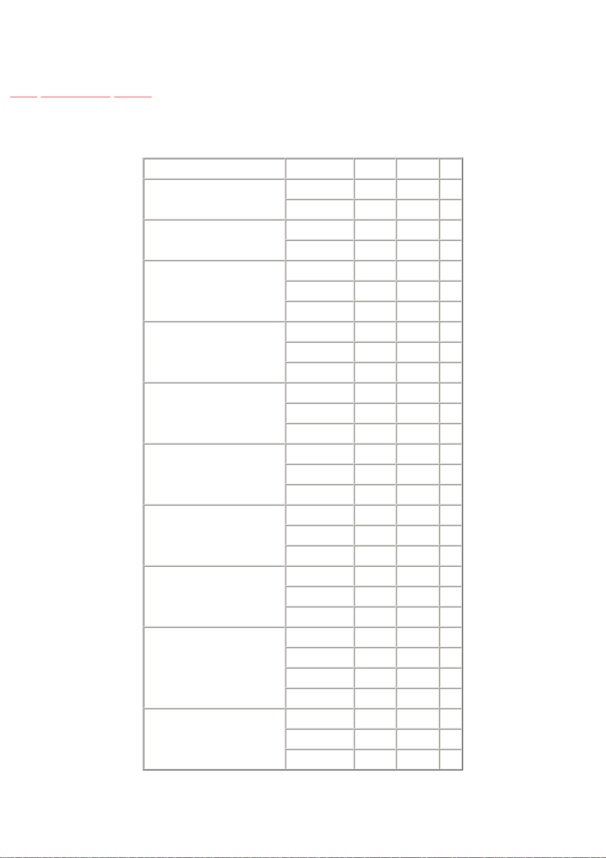
Below chart is mentioned different items for each models.
PARTS NAME PART NO. EB/EB1 EG/EG1 GN
MAIN P.C.B. REP2577C --- • •
REP2577D • --- ---
VIF DECODER P.C.B. VEP07A23S --- • •
VEP07A23T • --- ---
DIGITAL P.C.B. REP3391AC --- • ---
REP3391AE --- --- •
REP3391CE • --- ---
REAR PANEL RGR0328C-C --- • ---
RGR0328C-D • --- --RGR0328C-H --- --- •
FRONT PANEL ASS´Y2 RYP1142B-S --- • ---
RYP1142C-S • --- --RYP1142D-S --- --- •
DOOR(R) RKF0643F-S --- • ---
RKF0643G-S • --- --RKF0643J-S --- --- •
REMOTE CONTROL ASS´Y EUR7615KE0 • --- ---
EUR7615KD0 --- • --EUR7615KL0 --- --- •
AC CORD RJA0053-3X • --- ---
VJA0754 --- --- •
VJA1059 --- • ---
OPERATING INSTRUCTIONS RQT6597-B • --- ---
Note:
RQT6598-E --- • •
RQT6599-D --- • --RQT6600-J --- • ---
PACKING CASE RPG6046 --- • ---
RPG6047 • --- --RPG6176 --- --- •

Only DMR-HS2EB/EG have RAM disc as accesary.
However, this disc is not supplied as service part.
TOP PREVIOUS NEXT

1.2 Comparison for function
TOP PREVIOUS NEXT
Function DMR-HS2EB/EB1 DMR-HS2EG/EG1/GN
Owner ID • --Power Save --- •
Language --- •
Country --- •
TOP PREVIOUS NEXT

2 SAFETY PRECAUTIONS
TOP PREVIOUS NEXT
2.1 GENERAL GUIDELINES
2.1.1 LEAKAGE CURRENT COLD CHECK
2.1.2 LEAKAGE CURRENT HOT CHECK (See Figure 1 .)
TOP PREVIOUS NEXT

2.1 GENERAL GUIDELINES
TOP PREVIOUS NEXT
1. When servicing, observe the original lead dress. If a short circuit is found, replace all parts
which have been overheated or damaged by the short circuit.
2. After servicing, see to it that all the protective devices such as insulation barriers, insulation
papers shields are properly installed.
3. After servicing, make the following leakage current checks to prevent the customer from being
exposed to shock hazards.
2.1.1 LEAKAGE CURRENT COLD CHECK
2.1.2 LEAKAGE CURRENT HOT CHECK (See Figure 1 .)
TOP PREVIOUS NEXT
2.1.1 LEAKAGE CURRENT COLD
CHECK
TOP PREVIOUS NEXT
1. Unplug the AC cord and connect a jumper between the two prongs on the plug.
2. Measure the resistance value, with an ohmmeter, between the jumpered AC plug and each
exposed metallic cabinet part on the equipment such as screwheads, connectors, control shafts,
etc. When the exposed metallic part has a return path to thechassis, the reading should be
between 1MΩ and 5.2MΩ.
When the exposed metal does not have a return path to the chassis, the reading must be
.
TOP PREVIOUS NEXT
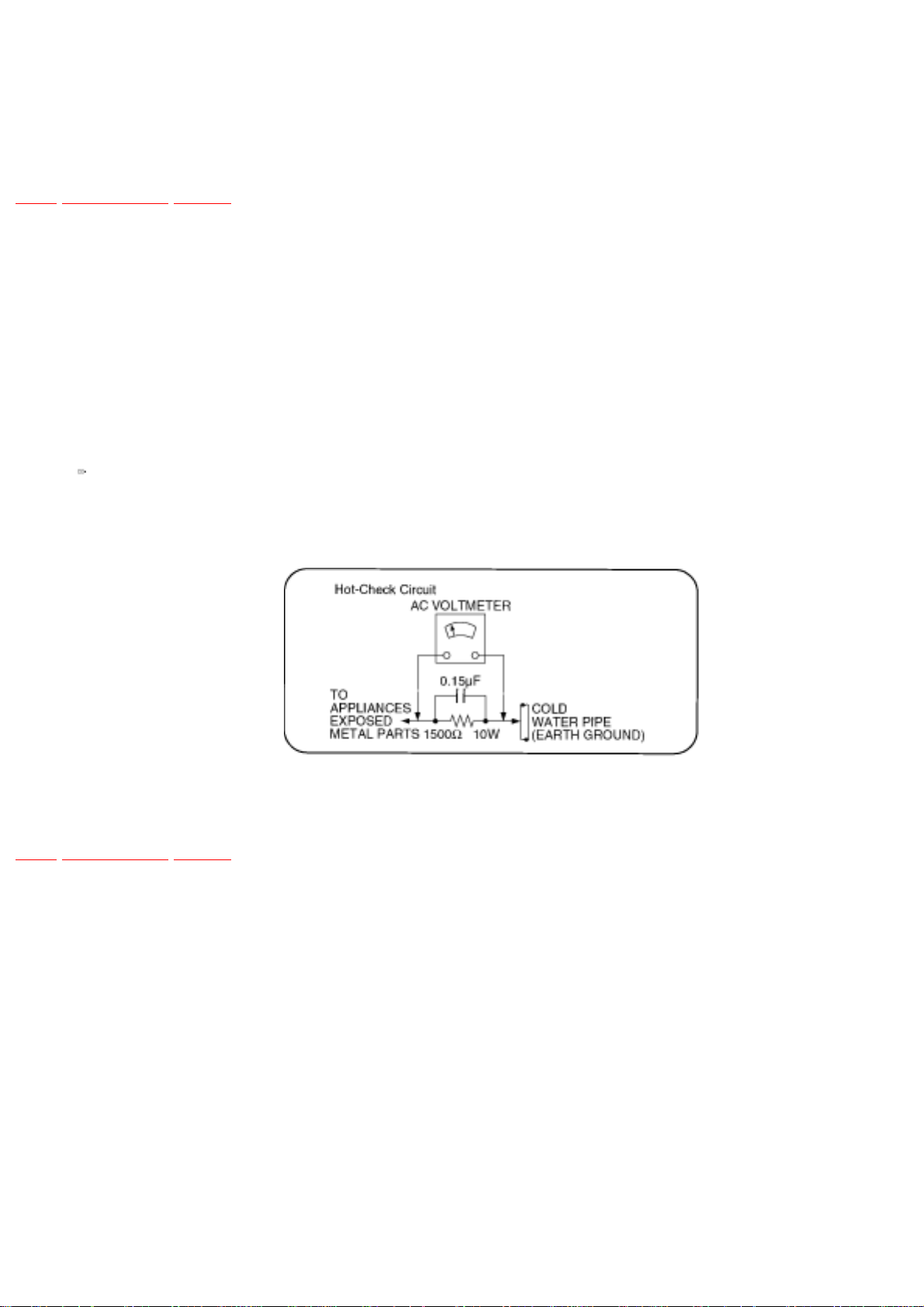
Figure 1

2.1.2 LEAKAGE CURRENT HOT CHECK
(See Figure 1 .)
TOP PREVIOUS NEXT
1. Plug the AC cord directly into the AC outlet. Do not use an isolation transformer for this
check.
2. Connect a 1.5kΩ, 10 watts resistor, in parallel with a 0.15•F capacitors, between each exposed
metallic part on the set and a good earth ground such as a water pipe, as shown in
3. Use an AC voltmeter, with 1000 ohms/volt or more sensitivity, to measure the potential across
the resistor.
4. Check each exposed metallic part, and measure the voltage at each point.
Figure 1 0.
5. Reverse the AC plug in the AC outlet and repeat each of the above measurements.
6. The potential at any point should not exceed 0.75 volts RMS. A leakage current tester
(Simpson Model 229 or equivalent) may be used to make the hot checks, leakage current
mu3st not exceed 1/2 milliamp. In case a measurement is outsideof the limits specified, there is
a possibility of a shock hazard, and the equipment should be repaired and rechecked before it is
returned to the customer.
TOP PREVIOUS NEXT

3 PREVENTION OF ELECTRO STATIC
DISCHARGE (ESD) TO
ELECTROSTATICALLY SENSITIVE (ES)
DEVICES
TOP PREVIOUS NEXT
Some semiconductor (solid state) devices can be damaged easily by static electricity. Such
components commonly are called Electrostatically Sensitive (ES) Devices. Examples of typical ES
devices are integrated circuits and some field-effect transistorsand semiconductor "chip" components.
The following techniques should be used to help reduce the incidence of component damage caused
by electro static discharge (ESD).
1. Immediately before handling any semiconductor component or semiconductor-equipped
assembly, drain off any ESD on your body by touching a known earth ground. Alternatively,
obtain and wear a commercially available discharging ESD wrist strap, whichshould be
removed for potential shock reasons prior to applying power to the unit under test.
2. After removing an electrical assembly equipped with ES devices, place the assembly on a
conductive surface such as alminum foil, to prevent electrostatic charge buildup or exposure of
the assembly.
3. Use only a grounded-tip soldering iron to solder or unsolder ES devices.
4. Use only an anti-static solder removal device. Some solder removal devices not classified as
"anti-static (ESD protected)" can generate electrical charge sufficient to damage ES devices.
5. Do not use freon-propelled chemicals. These can generate electrical charges sufficient to
damage ES devices.
6. Do not remove a replacement ES device from its protective package until immediately before
you are ready to install it. (Most replacement ES devices are packaged with leads electrically
shorted together by conductive foam, alminum foil or comparableconductive material).
7. Immediately before removing the protective material from the leads of a replacement ES
device, touch the protective material to the chassis or circuit assembly into which the device
will be installed.
Caution

Be sure no power is applied to the chassis or circuit, and observe all other safety precautions.
8. Minimize bodily motions when handling unpackaged replacement ES devices. (Otherwise
hamless motion such as the brushing together of your clothes fabric or the lifting of your foot
from a carpeted floor can generate static electricity (ESD) sufficient todamage an ES device).
TOP PREVIOUS NEXT
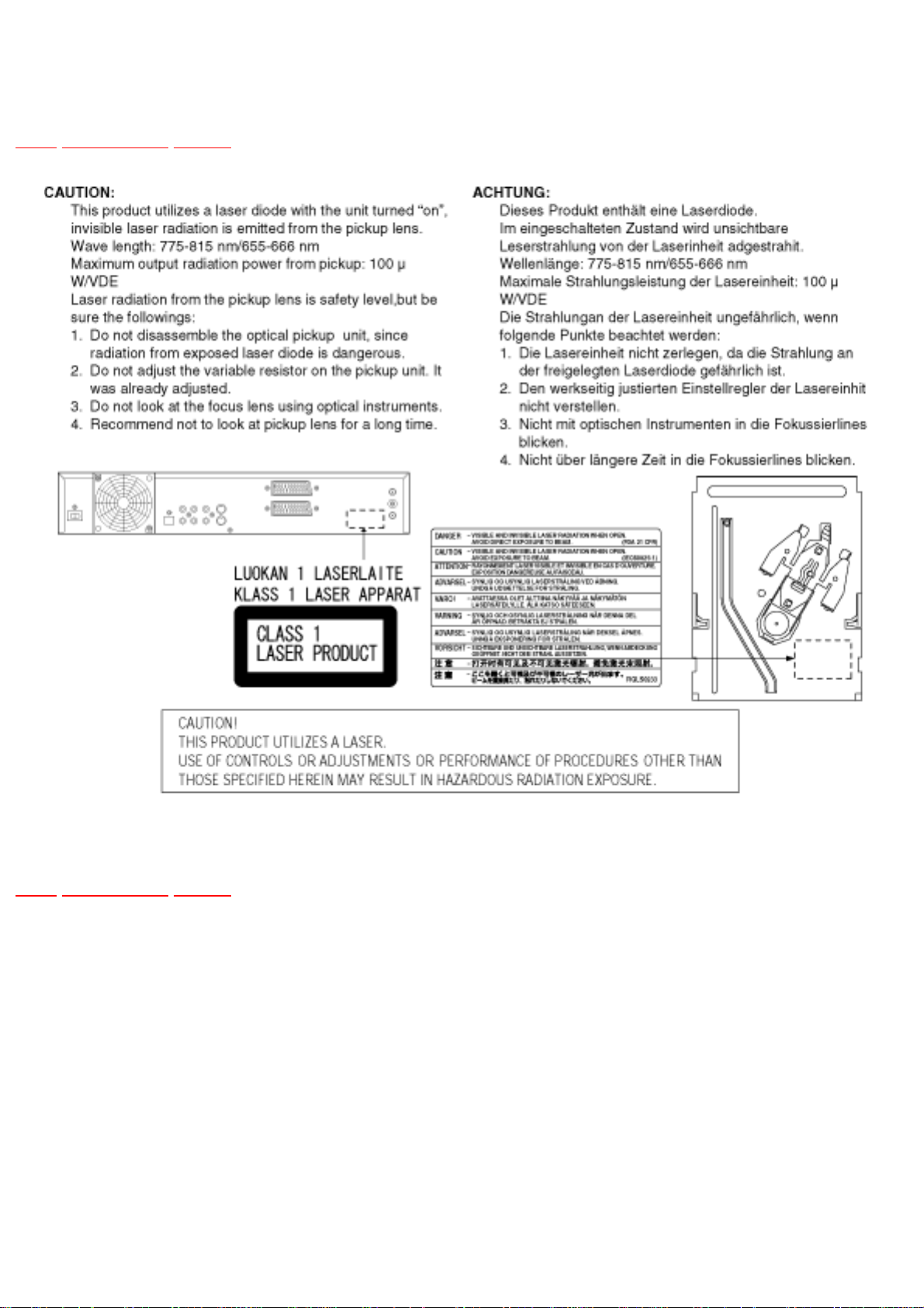
4 Precaution of Laser Diode
TOP PREVIOUS NEXT
TOP PREVIOUS NEXT

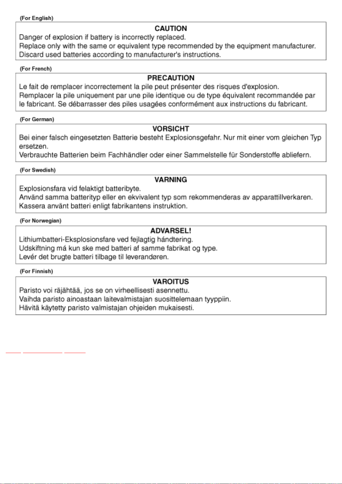
5 How to replace the Lithium Battery
TOP PREVIOUS NEXT
REPLACEMENT PROCEDURE
1. Remove the Top cover and DVD-RAM drive unit with Main P.C.B. by referring the
Disassembling Procedure.
2. Unsolder the Lithium Batteries: B7501 and then replace it into new one.
( As shown in 9.10. The Main P.C.B. )
NOTE:
The lithium battery is a critical component. ( Type No.: CR2354-1GUF Manufactured by Panasonic. )
It must never be subjected to excessive heat or discharge.
It must therefore only be fitted in equipment designed specifically for its use.
Replacement batteries must be of the same type and manufacture.
They must be fitted in the same manner and location as the original battery, with the correct polarity
contacts observed.
Do not attempt to re-charge the old battery or re-use it for any other purpose.
It should be disposed of in waste products destined for burial rather than incineration.
TOP PREVIOUS NEXT

6 Handling the Lead-free Solder
TOP PREVIOUS NEXT
6.1 About lead free solder (PbF)
TOP PREVIOUS NEXT

6.1 About lead free solder (PbF)
TOP PREVIOUS NEXT
Distinction of PbF P.C.B.:
P.C.B.s (manufactured) using lead free solder will have a PbF stamp on the P.C.B.
Caution:
● Pb free solder has a higher melting point than standard solder; Typically the melting point is 50
- 70°F (30 - 40°C) higher. Please use a high temperature soldering iron. In case of the soldering
iron with temperature control,please set it to 700 ± 20°F (370 ± 10°C).
● Pb free solder will tend to splash when heated too high (about 1100°F/600°C).
● When soldering or unsoldering, please completely remove all of the solder on the pins or
solder area, and be sure to heat the soldering points with the Pb free solder until it melts
enough.
TOP PREVIOUS NEXT
 Loading...