

Onkyo HT-RC260 (B) Service Manual
SERVICE MANUAL
AV RECIEVER
MODEL HT-RC260 (B)
HT-RC260
Ref. No. 4194
042010
Black model
120V AC, 60HzBMDC
SAFETY-RELATED COMPONENT
WARNING!!
COMPONENTS IDENTIFIED BY MARK ON THE
SCHEMATIC DIAGRAM AND IN THE PARTS LIST ARE
CRITICAL FOR RISK OF FIRE AND ELECTRIC SHOCK.
REPLACE THESE COMPONENTS WITH ONKYO
PARTS WHOSE PART NUMBERS APPEAR AS SHOWN
IN THIS MANUAL.
MAKE LEAKAGE-CURRENT OR RESISTANCE
MEASUREMENTS TO DETERMINE THAT EXPOSED
PARTS ARE ACCEPTABLY INSULATED FROM THE
SUPPLY CIRCUIT BEFORE RETURNING THE
APPLIANCE TO THE CUSTOMER.
RC-764M

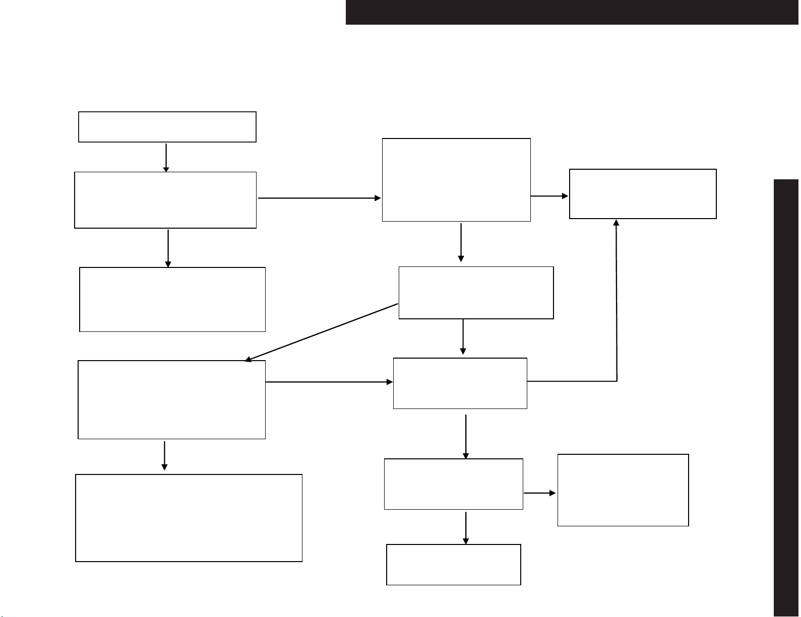
SERVICE PROCEDURE
1. Replacing the fuses
This symbol located near the fuse indicates that the
fuse used is show operating type, For continued protection against
fire hazard, replace with same type fuse, For fuse rating, refer to
the marking adjacent to the symbol.
Ce symbole indique que le fusible utilise est e lent.
Pour une protection permanente, n'utiliser que des fusibles de meme
type. Ce demier est indique la qu le present symbol est apposre.
<Notes>
Canadian model <MDC>:
HT-RC260
REF No.
PART NAME
DESCRIPTION PART N O. REMARKS
F6901 FUSE 12A-TUL-250V 1252301GR <B>
F6902 FUSE 12A-TUL-250V 1252301GR <B>
F901 FUSE 10A-UL/T-233 1252330GR <B MDC>
F901or FUSE 10A-T/UL-ST2 ( 1)252333GR <B MDC>
2. To initialize the unit
1. Press and hold down
2. After " C l e a r " is displayed, the preset memory and each mode stored in the memory are initialized and will
return to the factory settings, and turn to Standby mode.
3. Remove the AC cord from power line.
VCR/DVR
button, then press
ON/STANDBY
button when the unit is powered on.
3. Safety check out
(U.S.A. model only)
After correcting the original service problem, perform the following safety check before releasing the unit to
the customer.
Leakage current Check
Measure the leakage current to a known earth ground (water pipe or conduct etc.) by connecting a leakage current
tester between the earth ground and exposed metal parts of the unit (input/output ground terminals, screw heads or
metal overlays etc.).
Plug the power supply cord directly into a 120Vac 60Hz wall socket and turn
Any current measured must not exceed 0.5mA.
ON/STANDBY
button on.
4. Memory Backup
This model uses a EE-PROM IC in order to retain radio presets and other settings. So, memory contents will be
kept eternally with no care.
TX-SR308/ /508/ 578/ 608 HT-R280/ 380/ 538/ 580/ 680/ 980/ C230/ C260 DTR-20.2/ 30.2
TROUBLE SHOOT-1
No Power
No Power
BAETC-0376/0390 (Power supply)
BADG-0364 (MPU Board)
JL901 4pin +12V
2pin +10V
BAETC-0
Replace Power Supply Board orRepair
Sub Transformer T902 and itsperipheral
circuit.
376/0390 (Power supply)
NO
This is just for general reference and does not including every single case.
BAETC-0376/0390
(Power supply)
BADG-0364 (MPU Board)
YES
After Power on,
Voltage atJL901_1pin is changed
from +12V t o 0V?
NO
YES
BAETC-0376/0390
(Power Supply)
F901 is blown out?
YES NO
BADG-0364 (MPU Board)
Replace Q701 and also
repairits peripheral circuit.
TX-SR308/ /508/ 578/ 608 HT-R280/ 380/ 538/ 580/ 680/ 980/ C230/ C260 DTR-20.2/ 30.2
After replacing F901 on
BAETC-0376/0390
either of F901 on
or F6901/F6902 on BAAF-0341(AF
Board) blows out?
(Power supply)
Power supply
Board
Replacing F901 will not
improve the unit.
YES
BAAF-0355(AF Board)
Replace “AF Board”.
or “D6901 (Power supply diode)”
“Power AMP(Final_TR and A_Class AMP)
and also repair their peripheral circuit.
”
NO
BADG-0346 (MPU Board)
After Power on, Voltage at
P2001 22/21pin +5V
17/18pin +12V
NO
BAETC-0359/0352/0345/
(trans teminal Board)
After Power on, Voltage at
JL952 AC10V
NO
Replace Power
Transformer or
Repair its peripheral
circuit.
YES
YES
BAVD-0375/0389
(Video board)
Replace Video Board or
Repair D901/Q9023/Q9031
and their peripheral circuit.
TX-SR308/ /508/ 578/ 608 HT-R280/ 380/ 538/ 580/ 680/ 980/ C230/ C260 DTR-20.2/ 30.2
A
TROUBLE SHOOT- 2
No Display
1
Fluorescent Display Tube
is not working?
Replace Fluorescent
Display Tube or
2
BADIS-0373/0387(Display
Board).
BAPS-0342/0349/0356
(-VP Board)
Replace -VP Board or
Check for signal line
damage etc. and fix any
damages.
No Display
YES
BCDEFGH
This is just for general reference and does not include every single case.
The above waveforms are got by Oscilloscope of Maximum Horizontal Sensitivity: 100MHz.
The results depend on the oscilloscope.
NO
BAPS-0342/0349/0356(-VP Board)
JL953 between 2pin-4pin:
NO NO
BAPS-0342/0349/0356
(-VP Board)
JL951 1pin-2pin AC3.3V
YES
BAPS-0342/0349/0356
NO
(-VP Board)
R950(8.2 ) is disconnected?
YES
AC3.3V
YES
BAPS-0342/0349/0356 (-VP Board)
JL953 3pin -33V
1pin and 5pin +3.3V
BAPS-0342/0349/0356(-VP Board)
JL951 3pin-4pin AC40V
NO
NO
Replace Power transformeror
Repair its peripheral circuit.
YES
YES
BADIS-0373/ 0387
(Display
P701
26pin FLD_SDD
27pin FLD_CLK
28pin FLD_CS
Transmission of each
of the signals is
Board)
correct?
NO
BADG-0413(MPU Board)
Replace
or Repair Q701 and
their peripheral circuit.
MPU Board.
YES
BADIS-0373/ 0387
(Display
Replace Display Board
or repair Q7003 and
their peripheral circuit.
Board)
BAPS-0342/0349/0356 (-VP Board)
3
Replace R950 (8.2 ) or -VP Board
BAPS-0342/0349/0356 (-VP Board)
Replace -VP Board or
Q960/D960/D962/R961 and
their peripheral circuit.
Repair
FLD_CLK FLD_SDD(DATA) FLD_CS
V:1V/cm
H:02Msec/cm
4
Timing of Serial Communication
V:1V/cm
H:10µsec/cm
1 byte data
address data
1 byte data
data to be
V:1V/cm
H:1µsec/cm
5
TX-SR608 HT-RC260 DTR-20.2/ 30.2TX-SR608 HT-RC260 DTR20.2/ 30.2
Repair
A
TROUBLE SHOOT-3
No Sound
1
No Sound
from HDMI input
BAHDM-0403(HDMI Board)
P8001 16pin HDMI_SPDIF .
15pin HDMI_MCK
13pin HDMI_BCK
11pin HDMI_LRCK
9pin HDMI_FLR
Waveforms are no problem?
2
BADG-0403 (HDMI Board)
JL801
3
4
BAHDM-0403(HDMI Board)
Make sure that JL801 3pin is 12V
Replace HDMI Board
or Replace Q8501(HDMI_4RX)
Q81061(HDMI 1st SW)
5
or Repair its peripheral circuit.
NY Y
1&4pin +12V
YY
BAVD-0375/0389(Video)
Replace Video Board or Repair
D9011/R9013/R9012
and their peripheral circuit.
BCDEF GH
Note:
This is just for general reference and does not include every single case.
The above waveforms are got by Oscilloscope of Maximum Horizontal Sensitivity: 100MHz.
The results depend on the oscilloscope.
Y
N N
BAETC-0359 (torans terminal)
JL952 1-3pin
AC10V
Replace Power
transformer or
Repair its peripheral
circuit.
IJK
No Sound
from COASXL/OPT input
BAHDM-0403(HDMI Board)
DIR_OUT
P8001 3pin DIR_BCK
5pin DIR_LRCK
7pin DIR_FLR
P8002 23pin DIR_MCK
Waveforms are no problem?
BADG-0364(MPU Board)
DSP_OUT
P8002 24pin DSP_FL/R
P8001 8pin DSP_SL/R
,
10pin DSP_CSW
,
4pin CX_SCLK
.
6pin CX_LRCLK
Waveforms are no problem?
Y
NNN
BADG-0364(MPU Board)
P2001 21 22pin +5V
YY
BADG-0364(MPU Board)
Replace MPU Board or
Replace
U131/132 Q301 Q131 or
Repair their peripheral
N
BADG-0403(HDMI Board)
JL801
2pin and 4pin +12V
circuit.
Y
BAHDM-0401(HDMI Board)
Make sure that JL801 2pin & 4pin is
12V. Replace HDMI Board or
Replace Q2001(DSP-IC) or
Repair its peripheral circuit.
BAETC-0359(torans terminal)
JL952 1-3pin
BAVD-0375/0389(Video Board)
Replace Video Board or
Repair
Q9031/D9011/R9013/R9012
and their peripheral circuit.
N
BAETC-0359(torans terminal)
JL952 1-3pin AC10V
Y
BAVD-0375/0389(Video Board)
Replace Video Board or
Repair
D9011/9013/R9012
and their peripheral circuit.
AC10V
N
N
BADG-0364(MPU Board)
DAC_OUT
Analog signal outputs from 4-9
pins of P5502?
4pin----FR 5pin----FL
6pin----SW 7pin----C
8pin----SR 9pin----SL
NN
BADG-0364(MPU Board)
P2001 21 22pin +5V
BAETC-0359(torans terminal)
JL952 1-3pin
AC10V
N
YY
BADG-0364(MPU Board)
Y
Replace MPU Board or
Replace Q302 or
Repair its peripheral
circuit.
BAVD-0382/0389(Video Board)
Replace Video Board or
Repair
Q9031/D9011/R9013/R9012
and their peripheral circuit.
Replace Power
transformer or
Repair its peripheral
circuit.
No Sound
from ANALOG input
Y
BAAF-0355(AF Board)
AUDIO-SEL_OUT
Signal output is no problem?
Each PRE-OUT or
P6600 SBR--1pin SR--3pin
FR--5pin C------7pin FL--9pin
SL--11pin SBL---13pin
BATRM-0368(TRM Board)
JL600(AMP_OUT)
Signal output is no problem?
SR----6pin FR----5pin
C------4pin FL-----3pin
SL-----2pin SBR--7pin
SBL---1pin
Y
BATRM-0368(TRM Board)
JL603 1Pin +22V
Y
BADG-0364(MPU Board)
P5503 3pin (SEC1H)
Voltage changes from 0V to
3V about 2 or 3 seconds after
power-on?
Y
BATRM-0368(TRM Board)
JL610 1pin, 2pin, 3pin, 4pin
Voltage changes from 0V to
3V about 3 or 4 seconds
after power-on?
Y Y
BATRM-0368(TRM Board)
Replace TRM Board or
Repair
R6690, and their peripheral
circuit.
Q6601/6602/6603/6604
BAAF-0355(AF Board)
Q4170 3pin +5V
N
Q4171 3pin -15V
Q4184 E +7V
Q8185 E -7V
N
BCAF-0355(AF Board)
Replace AF Board or
Repair Q4170, Q4171, Q4181,Q4185
and
their peripheral circuit.
Y
BCAF-0355(AF Board)
Replace AF Board or
Repair Q4001 and its
peripheral circuit.
BCAF-0355(AF Board)
N
Replace AF Board or
Repair R4160/4166
D4300/4301/4302/4303 and
their peripheral circuit.
N
N
BCAF-0355 (AF Board)
NN
BADG-0364(MPU Board)
P5503 6pin(I-pro):0V
5pin(V-
8pin(V-olh):0V
JL501 3pin(THE): +1V or lower
pro):0V
P6901(+55V) P6902(-55V)
Y
N
BCAF-0355(AF Board)
Replace AF Board or
Repair Final TR
and their peripheral circuit.
BCAF-0355(AF Board)
BADG-0364(MPU Board)
Replace MPU Board or
Replace Q701 and repair
its peripheral circuit.
BACLA-0362
(A_Class amp Board)
Replace “A_Class amp Board”
and their peripheral circuit.
Replace AF Board or
Replace D6901 F6901
F6902 and repair their
peripheral circuit.
6
DIR_FLR DIR_LRCK DIR_BCK DIR_MCK
HDMI_SPDIF
DSP_FLR/SLR/CSW CX_LRCK CX_SCLK HDMI_MCK
HDMI_FLR HDMI_LRCK HDMI_BCK
7
V:1V/cm H:0.1µ/cm
V:1V/cm H:0.1µ/cm V:1V/cm H:5µ/cm V:1V /cm H:0.1µv/cm V:1V/cm H:0.1µv/cm
8
TX-SR578/ 608 HT-R680/ 980/ RC260 DTR-20.2/ 30.2
A
TROUBLE SHOOT-4
No Pictuer
1
2
BCDEFGH
Note:
This is just for general reference and does not include every single case.
No Picture from Analog
(COMPONENT/ S_VIDEO Input)
Y
No Picture from HDMI
(COMPONENT/S_VIDEO Input)
BADG-0403(HDMI Board)
P2801 2pin V out
4pin Y out
N
6pin B out
8pin R out
Video Signal OK?
No Picture from HDMI
(All HDMI Input)
No Picture from HDMI
(HDMI Input from 1 to 4)
Y
No Picture from HDMI
(Front HDMI Input)
BAVD-0375/0389
(Video Board)
JL952 1-3pin AC10V
3
BAVD-0375/0389
(Video Board)
Q9022 3pin +5V
YNY
Y
NN
N
Replace Power
transformer or
Repair its peripheral
circuit.
4
BAVD-0375/0389
(Video Board)
Replace Video Board or
Replace Q2001 and repair
its peripheral circuit.
BAVD-0375/0389
(Video Board)
Replace Video Board or
Replace Q9022 and repair
its peripheral circuit.
BAVD-0375(Video)
JL952 1-3pin AC10V
BAVD-0375/0389
(Video Board)
Replace Video Board or
Replace D9011/R9013
/R9012 and repair
its peripheral circuit.
BADG-0403(HDMI Board) JL801 2&4pin +12V
Y
BADG-0403(HDMI Board)
Q8200(cannot Replace)
Replace HDMI Board
or Replace Q8501/8801/8802
No Picture from HDMI
(COMPONENT/S_VIDEO Input)
BADG-0403(HDMI Board)
Q8200(cannot Replace)
Replace HDMI Board
or Replace Q8803/8804/8401
and repair its peripheral circuit.
/8803/8804/8806/8807 and repair
its peripheral circuit.
YY
Y
(All HDMI Input)
No Picture from HDMI
No Picture from HDMI
(HDMI Input from 1 to 4)
BADG-0403(HDMI Board)
Q8200(cannot Replace)
Replace HDMI Board
or Replace Q8161/8501/8801/8802
/8803/8804/8806/8807 and repair
its peripheral circuit.
Y
(Front HDMI Input)
No Picture from HDMI
BADG-0403(HDMI Board)
Q8200(cannot Replace)
Replace HDMI Board
or Replace Q8161/8501/8801/8802
/8803/8804/8806/8807 and repair
its peripheral circuit.
5
TX-SA578/ 578V/ 608 TX-SR508/ 608 HT-R680/ 980/ C260 DTR-20.2/ 30.2
A
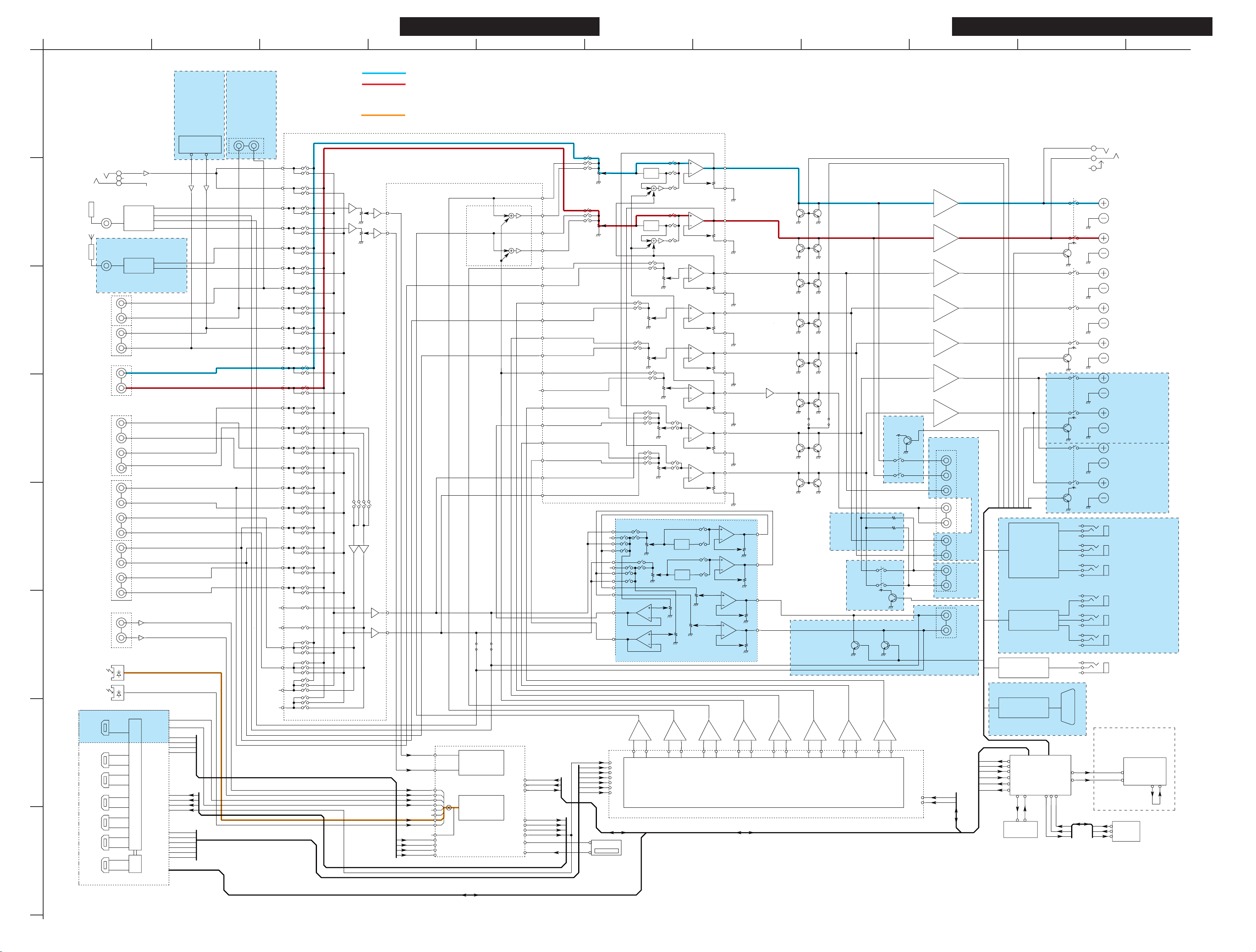
Reference materials
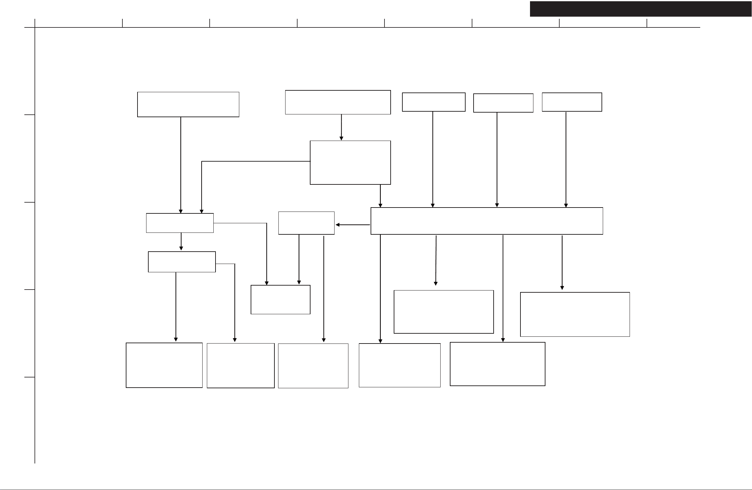
BLOCK DIAGRAMS (
1
2
3
4
5
BAHDM-0403 HDMI Board
TX-SR608, TX-SA608, HT-RC260,
DTR-20.2, DTR-30.2
PC VIDEO IN
ADIN(FFC)
TX-SR608, TX-SA608, DTR-30.2
HDMI
FRONT
TX-SR608, TX-SA608, HT-RC260,
DTR-20.2, DTR-30.2
HDMI IN5
HDMI IN4
HDMI IN3
HDMI IN2
HDMI IN1
BCDEFGH
HDMI Video & Digtal Audio Section)
RGB
VS,HS
I2C
ADINPY
ADINPB
ADINPR
ADINCV
GND
TMDS
CEC
DDC
+5V
HP DET
TMDS
CEC
DDC
+5V
HP DET
TMDS
CEC
DDC
+5V
HP DET
TMDS
CEC
DDC
+5V
HP DET
TMDS
CEC
DDC
+5V
HP DET
TMDS
CEC
DDC
+5V
HP DET
TMDS
CEC
DDC
RPWR
HPD
TMDS
CEC
DDC
RPWR
HPD
TMDS
CEC
DDC
RPWR
HPD
TMDS
CEC
DDC
RPWR
HPD
TMDS
CEC
DDC
RPWR
HPD
TMDS
CEC
DDC
RPWR
HPD
Q8661
TMDS141
Rx Tx
HDMI Buffer
Rx0
Rx1
Q8161
SiI9387
HDMI
Fast Switching
Rx2
Rx3
Rx4
I2S
Tx
I2C
CEC
TMDS
DDC
TMDS
DDC
RPWR
HPD
Rx3
Q8501
SII9233
HDMI
4Rx
Rx2
Rx1
Rx0
OP-1
OP-2
COAX-1
COAX-2
TTL
TC74VCX162827FT x2
12bit x3
Q301
DIR/ 2CH ADC
Q8806
Q8807
Bus switch
HDMI MCK
HDMI BCK
HDMI LRCK
HDMI FLR
HDMI S/PDIF
10bit x3
12bit x3
CH,BH,AH
AVS,AHS
I2C
Q8200
FLI32626
SEQUIOA
Video
Processor
B3P
SV3P
A2P
C4P
TTL in
ARC S/PDIF
TTL out
10bit x3
HDMI MCK
HDMI BCK
HDMI LRCK
HDMI FLR
PCMSLR_DR1
PCMCSW_DL1
PCMSBLR_DR2
HDMI S/PDIF
HDMI MCK
HDMI BCK
HDMI LRCK
HDMI FLR
Q205
TC74VHC157F
DIR MCK
CX LRCK
CX SCLK
DSP FLR
TC74VCX162827FT x4
PCMLRCK_DR0
PCMBCK_DSDCLK
MXK_HDMI
PCMLR_DL0
DIR MCK
Q8803
Q8804
Q8801
Q8802
Bus switch
DIR MCK
DIR BCK
DIR LRCK
DIR FLR
Q8401
12bit x3 DDC
PCMSLR_DR1
PCMCSW_DL1
PCMSBLR_DR2
HDMI S/PDIF
TTL Tx
Q201 DSP
DIR MCK
SII9136
HDMI
Tx
I2S
CEC
+5V Hot Plug
TMDS
CX LRCK
CX SCLK
DSP SBLR
DSP SLR
DSP CSW
DSP FLR
Q302 6CH DAC
HPD
TMDS
CEC
DDC
+5V
HP DET
ARC S/PDIF
HDMI OUT
SBL/ SBR
SL/ SR
C/ SW
FL/ FR
Q131 74HCU04F
ANALOG L/R
BADG-0403 MPU/DIR/DAC Board
TX-SA608 TX-SR608 HT-RC260 DTR-202./ 30.2
Reference materials, (protect detection)
SP_RLSB
SP_RLF
SP_RLZ2
SP_RLCS
1
Thermal Senser
LM61CIZ
G
2
O
V
3
Q6702
2SC2712-GR
220K
R6706
220K
R6716
Q6380
C6631
NM
PC board
33K
R6708
Q6701
2SC2712-GR
D6702
KDS4148U
C6706
21
10/50
D6701
D6704
UDZS3.3B
21
KDS4148U
C6701
100/25
5.6K
R6709
54.5V
NM
R6721
4.7K
R6710
MPU
GNDDG2
+3.3VMPU
THERMAL
VOLH
SEC1H
VPROTECT
IPROTECT
R6701
22K
1
2
3
R6702
2SA1163-BL
1/50
C6704
R6712
2SA1163-BL
1/50
C6714
10K
10K
C6703
Q6703
D6703
C6713
Q6713
D6713
Amplifier PC board
104Z
47K
R6704
UDZS3.3B
104Z
47K
R6714
UDZS3.3B
NPLG-2P29
ID+
ID-
1
3
P6080
(NH)
54.5V
2
1
-54.5V
T901
Q6050
2SC4468
2SC5242
R6140
56K
R6100
0.22(5W)
Q6060
2SA1695
2SA1962
D6000
KDS4148U
Power Amplifier PC board
IPRO
10K
R6150
R6170
12
S4
S3
S2
S1
Q6070
2SC2229
103J
C6050
47K
R6180
47K
R6160
SPL
NM
R6190
NM
D6010
1 2
VPRO
VOLH
+24V
AC_S1L+
33K
*
(1W)
8.2
R6197
AC S1H+
AC S1H-
SN5051
F6901
12A 250V
1
C6911
S1L+
47K
R6903
Q6707
2SC2712-GR
12
102J
D6902
+22V
R6902
1K
NRL-1P10A-DC12-196
1SS352
NRL-1P10A-DC12-196
104J
C6915
SP_RLCS
RL6902
4
3
5
5
3
4
RL6901
1
3
4 5
SP_RLF
Q6601
1
3
4
1
3
4 5
1
2
2
1
RL6600
RN1205
RL6602
RL6603
Q6602
RN1205
6
2
6
2
5
6
2
C6912
334J/100V
C6913
SPL
D10XB60H
334J/100V
D6901
SP_RLZ2
4
RL6605
1
3
4 5
Q6603
SP_RLSB
RL6607
1
3
4 5
Q6604
3
2
RN1205
RN1205
6
2
6
2
Speakers Terminal PC board
54.5V
-54.5V
TX-SA608 TX-SR608 HT-RC260 DTR-202./ 30.2
AC_S1L-
SN5051
F6902
104J
S1L-
1
C6916
Amplifier PC board
TX-SR578/ 608 HT-R680/ 980/ C260 DTR-20.2/ 30.2
MMPU/ VMPU/ DSP Update Procedure-1
Preparation for Update-1
1. PC(Personal Computer) which can play back wav files and output digital audio signal under Windows XP.
2. Software:Given wav-formatted FW Store it in the PC in advance (PC Update) or burn a CD-R with it as a music disc (CD Update).
3. Connection: DIGITAL (OPTICAL/COAXIAL) ourput of PC/CD Player --> DIGITAL (OPTICAL-1/COAXIAL-1) INPUT of TX-SR608 etc.
* PC needs to be able to handle wav files and output digital audio signal.
* For wav-compatible PCs which do not output audio signal at the above specification,
use a commercially-available USB-AUDIO interface unit. e.g. Onkyo-made ND-S1
* PC needs to run Windows XP. Windows Vista and Windows 7 do not work.
* Set wave Volume to Maximum including Volume Control in Control Panel.
For further information, please see Owner’s manual of your PC.
Control Panel
--> Sounds and Audio Devices
--> Volume tab
--> Advanced
* Instead of PC, CD players with DIGITAL output terminal can be used.
--> Turn all the levels to Max.
Note: CD players need to output digital audio signal .
Some CD players and DVD players are not suitable for update because they process audio signal to output.
Burn a CD-R as music disc.
Connection Example
PC(Personal Computer)
USB cable
SYNC/
UNSYNC
PC
d
o
P
i
T
R
O
P
S
N
A
R
Y
B
D
d T
N
o
A
T
iP
S
Y
B
D
N
A
T
S
/
N
O
For a different shape of OPTICAL terminal,
Use a conversion adapter.
DIGITAL
OUT
OPTICAL
DIGITAL
OUT
OPTICAL
OPTICAL
1
(VCR/DVR)
Rear Panel
USB-AUDIO interface unit. e.g. Onkyo-made ND-S1
ANALOG
DIGITAL
OUT
OPTICAL
OUT
REMOTE
CONTROL
DIGITAL
L
OUT
OPTICAL
OPTICAL
1
(VCR/DVR)
CD player
R
Rear Panel
<NOTE 1>
When not display it about 20 seconds later "Writing” .
right digitalaudio signal is not output.
Check the connection and settings and try again.
When another try results in failure again, use the other update method.
<NOTE 2>
DURING FW UPGRADE, DO NOT TURN OFF THE UNIT. DO NOT REMOVE ANY CONNECTIONS.
These operation will not allow FW Upgrade any more, and the whole board or IC will need replacing.
TX-SR578/ 608 HT-R680/ 980/ C260 DTR-20.2/ 30.2
MMPU/ VMPU/ DSP Update Procedure-2
Update Procedure
While the unit is on, hold down [DISPLAY] and then press [ON/STANDBY].
1.
Main FW Version will be shown on Front Display.
e.g.
2.
While Main FW Version is shown, press [+(TONE)].
DSP FW Version will be shown on Front Display.
e.g.
3.
While DSP FW Version is shown, press [RETURN].
M:1.02/10323AE
D:1.02/10416a38
AUTO ALL
* It depends on the version.
* It depends on the version.
ON/STANDBY
TUNING
* TUNING key changes “AUTO COAX1 OPT1.”
(”AUTO” means “COAX1” or “OPT1” will be automatically detected.
* TUNING key changes “ALL MMPUVMPUDSPVSPPORT”.
(TOTAL = MMPU+VMPU+DSP+VSP+PORT)
4. When MMPU VMPU and DSP FWs are upgraded at the same time, select “AUTO ALL” and press “ENTER.”
*The FW data please use Package Wev file.
For separate upgrade, select “MMPU” “VMPU” or “DSP”
and please “ENTER.”
*The partial renewal cannot use Package Wev file.
Please use individual Wav File.
5. PC upgrade: Play back the stored wav file in your PC.
CD upgrade: Play back the FW CD-R with the connected CD player. It takes about 15 minutes.
[NOTE] Make sure that ”dolby dts” is shown before starting playback.
About 20 seconds later, the message will change from S/PDIF Update... to Writing...
When “Writing...” will not be shown, the output music data is not correct.
Check the connection and settings.
S/PDIF Update..
S/PDIF Update..
(about 20 seconds)
Playback starts. (Playback time: about 20 minutes)
+(TONE)
DISPLAY
ENTER
RETURN
DSP Writing...
VMPU Writing
MMPU Setting
FW-Update00000
FW-UpdateFF000
OK:Sum=*************
6. Unplug AC cord and plug it again. Press [ON/STANDBY].
After playback finishes, update will start.
(just after “FF000” is shown)
“********” depends on the version.
Clear
7. Make sure that “Clear” is shown and the unit is turned into the Standby mode.
8. Make sure that the FW versions are the latest.
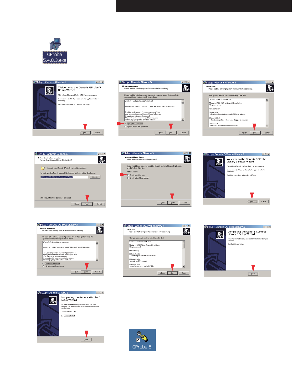
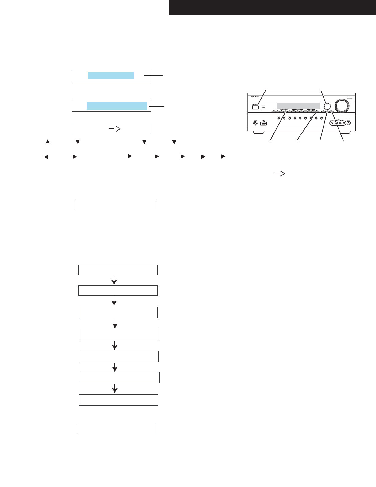
VSP Update Procedure-1
Click the Gprobe exe and begin installation
TX-SR578/ 608 HT-R680/ 980/ C260 DTR-30.2/ 20.2
3
6
Click
Check
Check
2
Click Click
5
Click
1
Click
4
Click
78
Click
10
Click
Click
Icon is displayed to a desktop.
9
Click

TX-SR578/ 608 HT-R680/ 980/ C260 DTR-30.2/ 20.2
VSP Update Procedure-2
㪈 㪤㪸㫂㫀㫅㪾㩷㪙㪸㫋㪺㪿㩷㪽㫀㫃㪼
㪈㪅㪈 㪚㫉㪼㪸㫋㩷㪸㩷㪽㫆㫃㪻㪼㫉㩷㫋㪿㪸㫋㩷㪙㪸㫋㪺㪿㩷㪽㫀㫃㪼㩷㪸㫅㪻㩷㪦㪹㫁㪼㪺㫋㩷㪽㫀㫃㪼㫊㩷㪸㫉㪼㩷㫇㫌㫋㪅
㪠㫅㩷㫋㪿㪼㩷㪼㫏㪸㫄㫇㫃㪼㩷㪹㪼㫃㫆㫎㪃㩷㩷㫋㪿㪼㩷㪽㫆㫃㪻㪼㫉㩷㫅㪸㫄㪼㪻㩷㪪㪼㫈㫌㫆㫀㪸㩿㪘㫉㪹㫀㫋㫉㪸㫉㫀㫅㪼㫊㫊㪀㩷㫀㫊㩷㫄㪸㪻㪼㩷㫌㫅㪻㪼㫉㩷㪚㩷㪻㫉㫀㫍㪼㪅
㪈㪅㪈㪅㪈 㪠㫅㩷㫋㪿㫀㫊㩷㪽㫆㫃㪻㪼㫉㪃㩷㫇㫌㫋㩷㫋㪿㪼㩷㫋㫏㫋㩷㪽㫀㫃㪼㩷㪸㫅㪻㩷㫋㪿㪼㩷㪿㪼㫏㩷㪽㫀㫃㪼㫊㩷㫊㫌㪺㪿㩷㪸㫊㩷㪹㪼㫃㫆㫎㪅㩷
㫀㫊㫇㪶㫊㫇㫀㪶㪼㫏㫋㪶㪍㪋㪤㪅㫋㫏㫋
㫀㫊㫇㪶㫊㫇㫀㪶㪼㫏㫋㪶㪍㪋㪤㪅㪿㪼㫏
㪘㪜㪶㪪㫀㪾㪶㪙㪝㪅㪿㪼㫏
㪪㪼㫈㫌㫆㫀㪸㪦㪥㪢㪶㪈㪇㪊㪇㪌㪸㪅㪿㪼㫏
㪧㫃㪼㪸㫊㪼㩷㪻㫆㫎㫅㫃㫆㪸㪻㩷㫋㪿㪼㫊㪼㩷㪽㫀㫃㪼㫊㩷㪽㫉㫆㫄㩷㫋㪿㪼㩷㪩㪼㫃㪼㪸㫊㪼㩷㪻㪸㫋㪸㩷㪹㪸㫊㪼㩷㫊㪼㫉㫍㪼㫉㪅
㪧㫃㪼㪸㫊㪼㩷㪺㪿㪸㫅㪾㪼㩷㫋㪿㪼㩷㫅㪸㫄㪼㩷㫆㪽㩷㫋㪿㪼㩷㪿㪼㫏㩷㪽㫀㫃㪼㩷㩿㫌㫅㪻㪼㫉㫃㫀㫅㪼㪻㩷㫀㫅㩷㫋㪿㪼㩷㪼㫏㪸㫄㫇㫃㪼㩷㪹㪼㫃㫆㫎㪀㩷㫀㫅㩷㩾㫀㫊㫇㪶㫊㫇㫀㪶㪼㫏㫋㪶㪍㪋㪤㪅㫋㫏㫋㩾㩷㫇㫉㫆㫇㪼㫉㫃㫐
㪸㪺㪺㫆㫉㪻㫀㫅㪾㩷㫋㫆㩷㫋㪿㪼㩷㫍㪼㫉㫊㫀㫆㫅㪅
㪫㪿㪼㩷㪼㫏㪸㫄㫇㫃㪼㩷㪹㪼㫃㫆㫎㩷㪼㫏㫇㫃㪸㫀㫅㫊㩷㫋㪿㪼㩷㫅㪸㫄㪼㩷㫇㪸㫉㫋㫀㫋㫀㫆㫅㫊㩷㫆㪽㩷㫋㪿㪼㩷㪿㪼㫏㩷㪽㫀㫃㪼㪑
㪪㪼㫈㫌㫆㫀㪸㪦㪥㪢㪶㪈㪇㪊㪇㪌㪸㪅㪿㪼㫏
㪪㪼㫈㫌㫆㫀㪸㩷㪑㩷㩷㪸㪺㫉㫆㫅㫐㫄㩷㪽㫆㫉㩷㫋㪿㪼㩷㪭㫀㪻㪼㫆㩷㪧㫉㫆㪺㪼㫊㫊㫆㫉㩷㪚㪿㫀㫇㩷㪪㪼㫈㫌㫆㫀㪸
㪈㪇㪊㪇㪌㪸㪑㩷㩷㩷㪫㪿㪼㩷㪽㫀㫉㫄㫎㪸㫉㪼㩷㫉㪼㫃㪼㪸㫊㪼㩷㪻㪸㫋㪼㪅㩷㪫㪿㪼㩷㪽㫀㪽㫋㪿㩷㫆㪽㩷㫄㪸㫉㪺㪿㩷㪉㪇㪈㪇
VSP Update Procedure-3
2. Connection
2.1 PC(RS232C COM Port) Connection
Connect PC and RS232C straight cable.
Connect Conversion board to flat cable and that RS232C straight cable.
TX-SR578/ 608 HT-R680/ 980/ C260 DTR-20.2/ 30.2
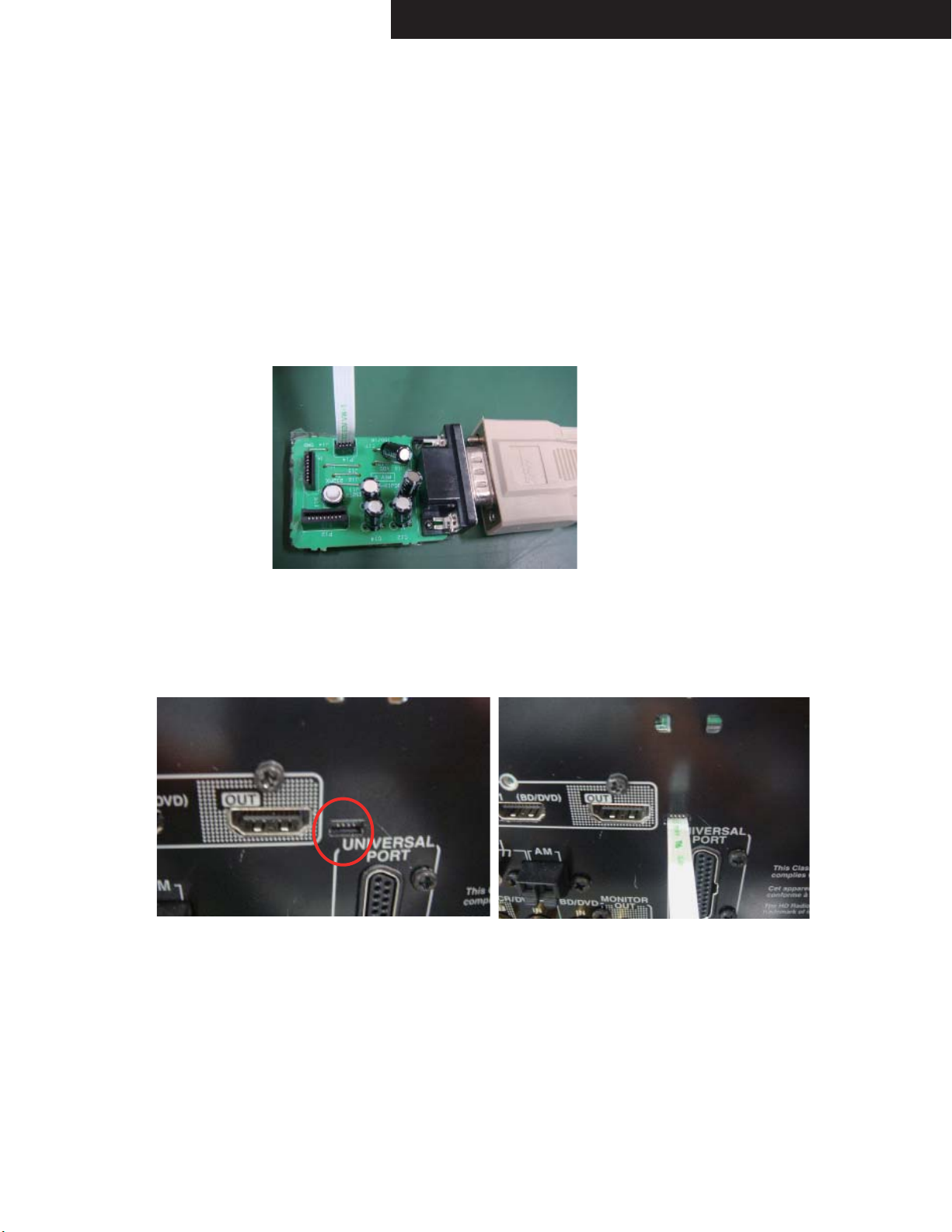
2.2 Unit(Rear Panel Slit) Connection
Connect the flat cable into the connecter in the slit of the rear panel..
㩷
TX-SR578/ 608 HT-R680/ 980/ C260 DTR-30.2/ 20.2
VSP Update Procedure-4
3 Execution of Gprobe
3.1 Click the Gprobe icon and start it.
3.2 Turn on the power supply of AVR.
䇭 If a Log message comes out the red icon shown below appears, it is connected properly.
Please wait for the output of a message to stop before writing the FW.
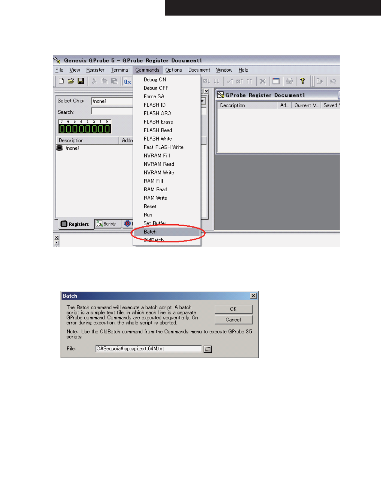
3.3 Batch
3.3.1To click [Commands] in top tool bar.
VSP Update Procedure-5
3.3.2Click [Batch] in [Commands].
TX-SR578/ 608 HT-R680/ 980/ C260 DTR-30.2/ 20.2
3.3.3Choose the batch file that you should write in and click OK.
The file to choose then is text file 㩹㫀㫊㫇㪶㫊㫇㫀㪶㪼㫏㫋㪶㪍㪋㪤㪅㫋㫏㫋㩹㩷㫀㫅㩷㩹㪪㪼㫈㫌㫆㫀㪸㩷㪽㫆㫃㪻㪼㫉㩹㩷㫎㪿㫀㪺㪿㩷㫐㫆㫌㩷㫄㪸㪻㪼㩷㫊㫆㫄㪼㩷㫋㫀㫄㪼㩷㪸㪾㫆㪅
TX-SR578/ 608 HT-R680/ 980/ C260 DTR-20.2/ 30.2
VSP Update Procedure-6
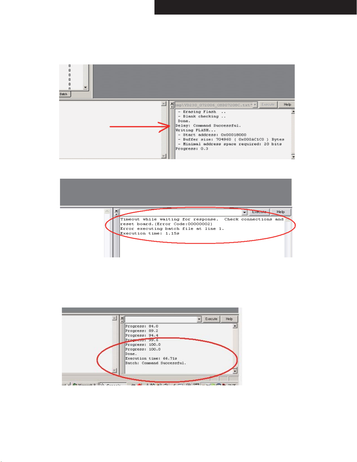
2.3.4Writing begins when "Command Successful. Writiing FLASH. . ." is displayed
If the below message appears, the writing process has failed. Please try again.
3.3.5Batch completion (writing completion).
If the message named "Command Successful" appears as follows, the writing process is done.
Please OFF/ON the power supply.
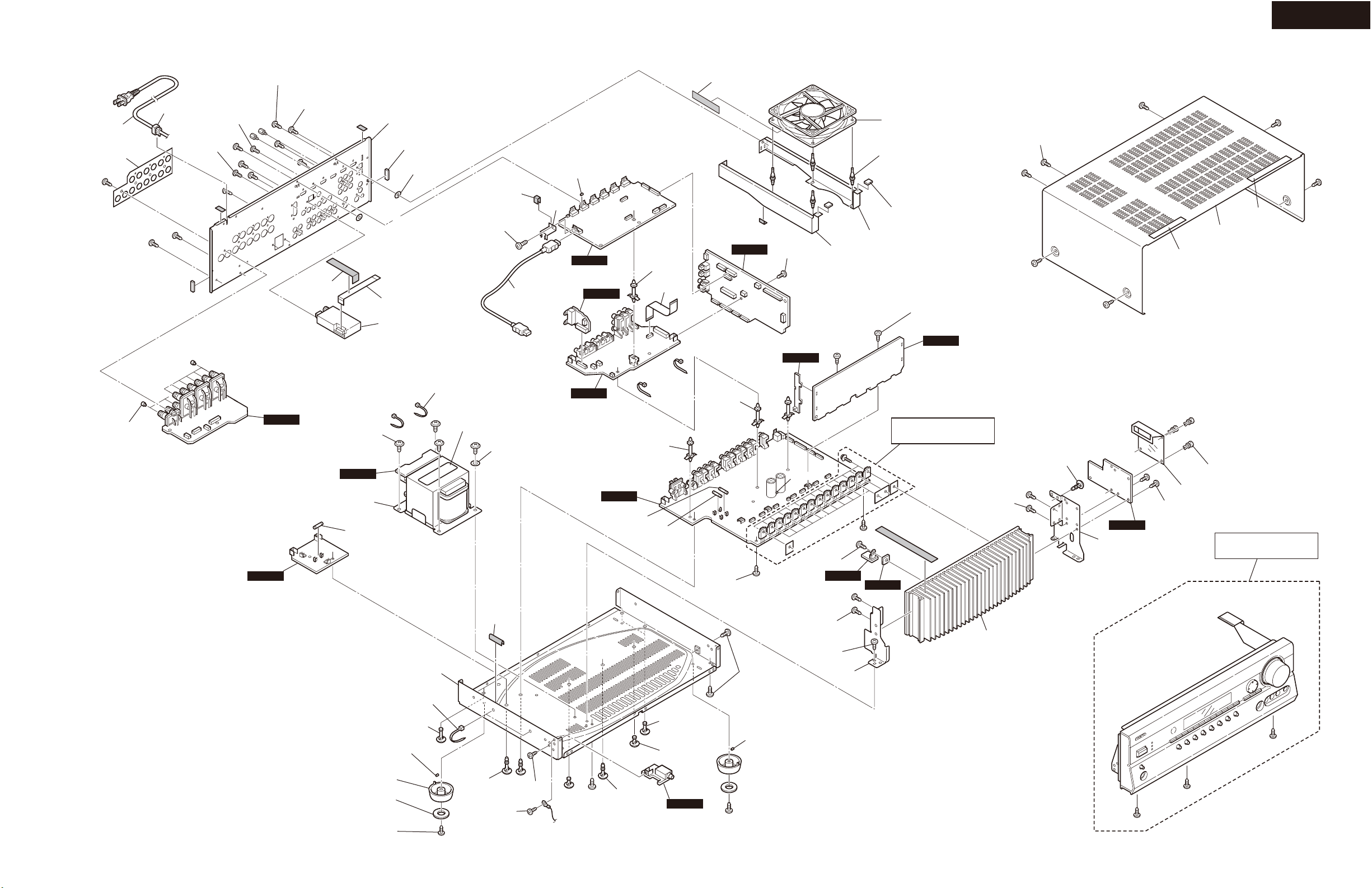
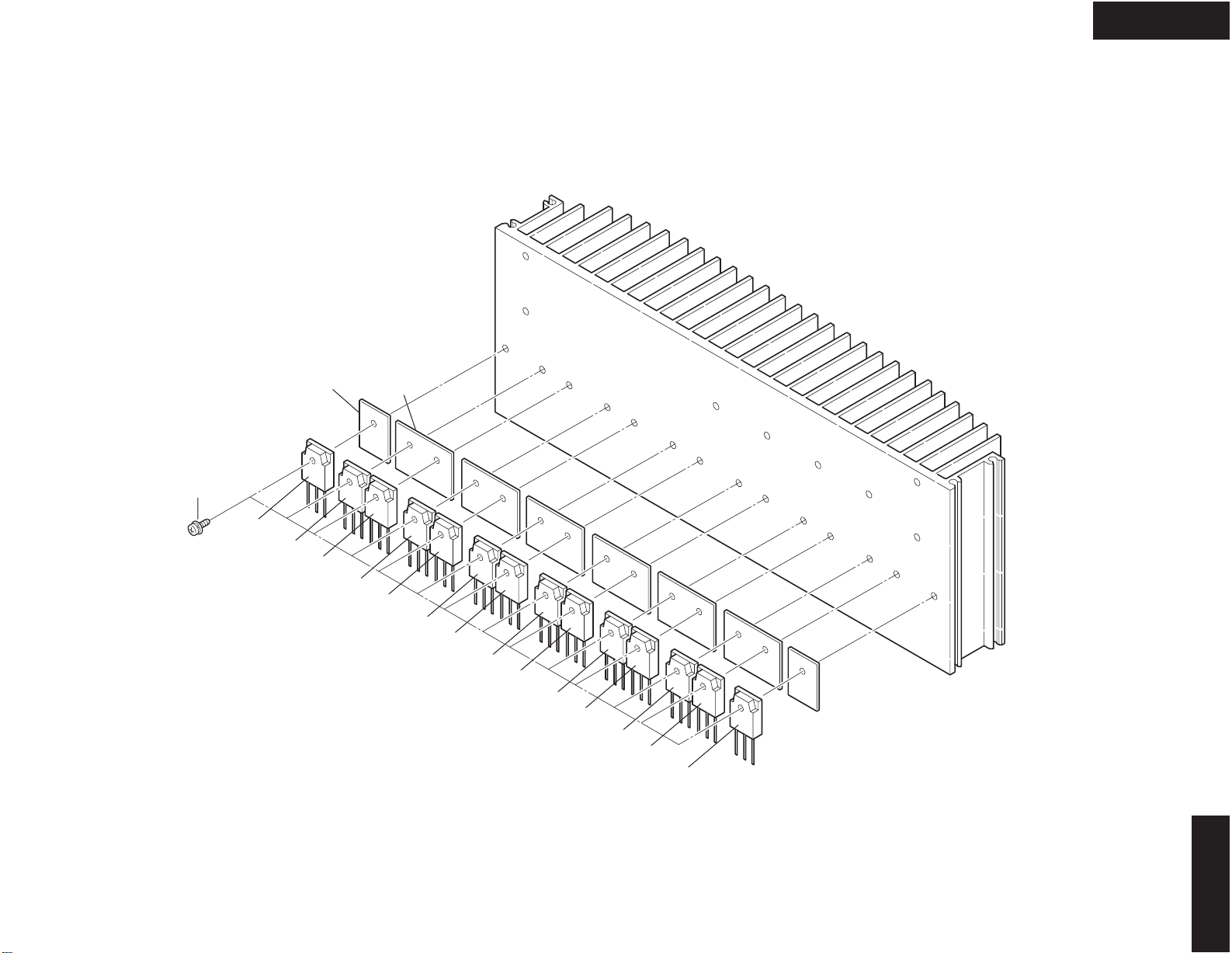
EXPLODED VIEWS-1
HT-RC260
P901
A070
P6601A
x 18 pcs.
A056
A103
x 6 pcs.
A109
x 2 pcs.
U0060
U0043
A1097
x 2 pcs.
A105
x 29 pcs.
A261
A025
x 4 pcs.
U0014
T901
F901
A101
P101
U010
A102
x 2 pcs.
A098
x 2 pcs.
A254
x 9 pcs.
A058
A323
A283
A027
P8651
A281
A104
U0070
U0042
U0031
U0010
F6901
A011
P2801
A023
F6902
A053
U0030
A021
x 2 pcs.
A040
x 2 pcs.
A069
U0021
A287
A091
A054
U0012
A093
U0013
P2510
A095
x 4 pcs.
A099
x 2 pcs.
A068
x 4 pcs.
U0020
Refer to
EXPLODED VIEWS-3
A036
x 2 pcs.
A342
x 7 pcs.
A044
U0064
A034
A362
A051
A040
x 2 pcs.
A360
A340
A052
x 3 pcs.
Refer to
EXPLODED VIEWS-2
A006
x 2 pcs.
A003
x 4 pcs.
A005
x 4 pcs.
A007
x 4 pcs.
A001
A060
x 2 pcs.
A019
A017
A002
A256
x 3 pcs.
A256
A009
x 2 pcs.
A013
x 2 pcs.
A010
x 2 pcs.
U0044
A040
x 2 pcs.
A006
x 2 pcs.
A036
x 2 pcs.
A038
x 2pcs.
A032
A030
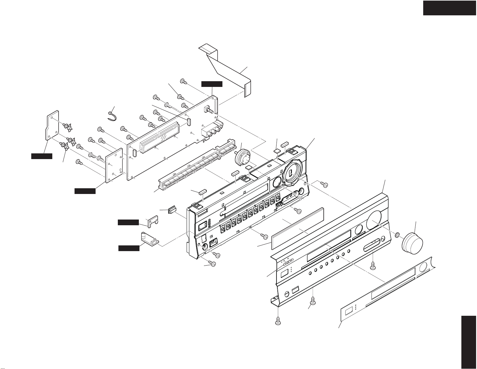
EXPLODED VIEWS-2
HT-RC260
<Fig-1>
U0011
A273
x 3 pcs.
U0041
A254
x 5 pcs.
U0072
A221
A215
A217
A223
x 22 pcs.
A264
x 3 pcs.
U0040
P701
A219
A099
x 2 pcs.
A211
A201
A321
U0071
A255
x 5 pcs.
A250
A207
A260
x 3 pcs.
HT-RC260
A202
EXPLODED VIEWS-3
<Fig-2>
HT-RC260
A050
x 14 pcs.
Q6056
Q6050A
x 2 pcs.
Q6066
Q6054
Q6050B
x 6 pcs.
Q6064
Q6051
Q6061
Q6052
Q6062
Q6050
Q6060
Q6053
Q6063
Q6055
Q6065
HT-RC260
TX-SA608/ TX-SR608/ HT-RC260
A
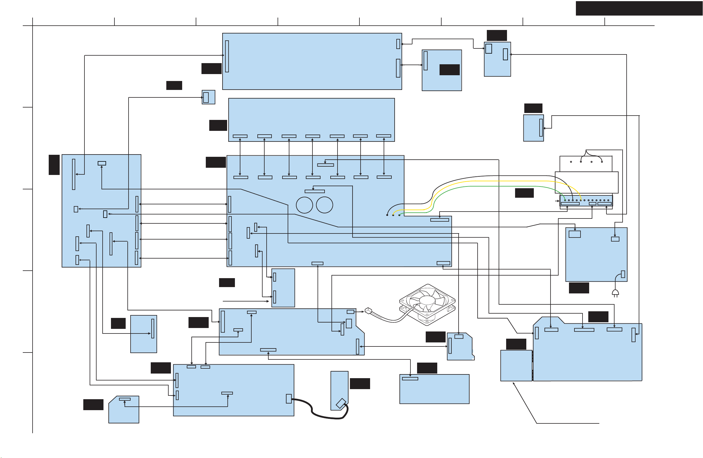
WIRING DIAGRAM
1
2
U0030
JL501B
MPU/DAC BADG-0364
3
P8002A
P8001A
4
31P FFC
P701A
31P FFC
P101A
JL610B
3P CABLE
JL901B
P2001A
11P FFC
U010
24P SOCKET
16P SOCKET
(
U010, Deletion:
BCDEFGH
P5504A
P5503A
P5502A
P5501A
TUNER
UNIT
Japanese model)
U0070
U0012
5P CABLE
7P SOCKET
5P CABLE
9P SOCKET
15P SOCKET
7P SOCKET
31P FFC
U0040
BAETC-0357
JL501A
U0020
U0010
24P SOCKET
U0042
9P FFC
P2801B
JL801B
P701B
P6006A
P6006A
P5504B
P5503B
P5502B
P5501B
U0032
(Japanese
Model Only)
P2801A
P2001B
5P CABLE
DISPLAY
BADIS-0373
AMP(MAIN INPUT)
BACLA-0362
P6004A P6003AP6000A
9P SOCKET 9P SOCKET
P6004A P6003AP6000A
P5507B
JL502A
P5506B
5P SOCKET
JL801A
P6001A
P6001A P6005A
3P SOCKET
P5507AP5506A
VLSC
P6002A
9P SOCKET
P6002A
JL603A
C6901
BAETC-0366
VIDEO
BAVD-0375
P2900A
15P CABLE
9P SOCKET
JL600A
C6902
5P CABLE
5P CABLE
3P CABLE
9P SOCKET
5P CABLE
JL503A
P2510
JL503B
JL952B
P2002A
9P SOCKET
AMP
BAAF-0355
TO FAN
P6005A
9P SOCKET
P6900B
JL953A
JL702A
P6903B
P6904B
9P CABLE
5P CABLE
JL702B
BADIS-0374
JL954B
JL604B
U0031
U0062
U0041
U-PORT
BAETC-0365
JL502B
P2002B
15P SOCKET
U0011
-VP
BAPS0356
9P CABLE
5P CABLE
JL953B
JL951B
BLK CABLE
YEW CABLE
GRN CABLE
7P CABLE
U0061
Z2 SP TRM
BATRM-0368
5P CABLE
U0044
HP JACK
U0014
TRANS TRM
BAETC-0359
JL605A
BAETC-0377
9P CABLE
5P CABLE
JL604B
JL610A
5P CABLE
POWER TRANS
P961:P6904A
P959:P6900A
P957:P6903A
P961
3P CABLE
P956
P960
P959
P957
P958
P955
JL954A
JL901A
POWER SUPPLY
BAETC-0376
U0043
7P CABLE
9P CABLE
U0060
JL603B
SP TRM
SP TRM
BATRM-0368
BATRM-0368
P954
P953
P952
JL952A
P951
P950
JL951A
JL600B
2P CABLE
P911
P901
5P CABLE
JL605B
P8002B
5
U0063
P4900A
P8001B
11P FFC
D-SUB
BAETC-0371
P4900B
P8651
P8662
HDMI
BAHDM-0403
HDMI CABLE
U0071
FRONT HDMI
BAHDM-0404
P2900B
(Japanese Model Only)
D-TERMINAL
BAVD-0370
U0061
Deletion:Canadian Model
USA Model
Taiwanese Model
TX-SA608 TX-SR608 HT-RC260 DTR20.2 DTR-30.2
TX-SA608 TX-SR608 HT-RC260 DTR20.2 DTR-30.2 DTR-20.2/30.2
A
BLOCK DIAGRAMS-1c
AUDIO BLK SECTION
1
FRONT BOARD
MIC
2
3
4
VCR/DVR OUT
5
6
7
8
UPORT OPTION UNIT
SXM ANATENA
AUX IN
(FRONT IN)
TUNER
(MJJ ONLY)
TV/CD
GAME
CBL/SAT
VCR/DVR
DVD/BD
COAX 1
COAX 2
OPT1
OPT2
EXCEPT:DTR-20.2
IN
(FRONT HDMI)
IN5
IN4
HDMI
IN3
IN2
IN1
OUT
UNIVERSAL PORT
UPORT
SXM
ONLY:TX-SR608/DTR-30.2
(
Canadan,USA model)
PC
HDMI
HDMI
MIC AMP
Q7401
MIC DET
SXM
RX
(BL/BR)
(SL/SR)
(CT/SW)
(FL/FR)
TX
U PORT L
ZONE2 L
ZONE2 R
U PORT R
ARC_SPDIF
HDMI_SPDIF
HDMI MCK
HDMI BCK
HDMI LRCK
HDMI FLR
DIR BCK
DIR LRCK
DIR FLR
DIR MCK
CX LRCK
CX SCLK
DSP SBLR
DSP SLR
DSP CSW
DSP FLR
BCDEF GH
AUDIO ANALOG SIGNAL(TV/CD)
FRONT L
FRONT R
EXCEPT:
Japanese model
TUNER
PACK
SPI to Micom
EXCEPT:
DTR-30.2/20.2
(FRONT IN)
MINI JACK IN
85
86
81
82
73
72
78
79
70
71
68
69
66
67
64
65
62
63
60
61
58
59
90
91
75
76
84
83
MAIN L
MAIN R
SUB L
DIGTAL
REC R
REC L
AUDIO SIGNAL(OPT-1)
54
55
47
46
Z2 L
Z2 R
Q4003
Downmix
FL/FR -12dB
SW +3.5dB
SR607/RC260 ONLY
PCM9210
HDMI MCK
HDMI BCK
HDMI LRCK
HDMI FLR
47
48
29
28
3
4
2ch ADC
DIR
31
30
15
7
8
9
10
Q301
RTAD
RTAD
LTAD
SR607/RC260
ONLY
INVERTING
INVERTING
SBL
SBR
(SR)
SR
(SL)
SW
(SBR)
25
24
23
19
18
17
20
40
39
(FR)
FL
CEN
SL
(SBL)
X-TO
X-Tl
94
43
93
(FL)
42
FR
95
38
98
41
97
40
96
39
100
37
99
36
44
45
C
FR
DIG CLK
DIG SD0
DIG SD1
DIR BCK
DIR LRCK
DIR FLR
DIR MCK
Zone2 out(L-ch)
Zone2 out(R-ch)
Zone2 in(R-ch)
SBL
SBR
SL
SR
SW
FL
MCLK
Zone2 in(L-ch)
Q4001
3
28
30
26
2
29
27
31
4
5
39
40
EXCEPT:TX-SR608/TX-SA608/HT-RCRC260
Q401A
LPF
14
DIR MCK
CX LRCK
CX SCLK
DSP SBLR
DSP SLR
DSP CSW
DSP FLR (FL/FR)
6
7
8
9
10
11
X171-XTAL
24.576MHz
SPI
(BL/BR)
(SL/SR)
(CT/SW)
R2A15218FP
TONE
TONE
ZONE2 FUNCTION
TONE
TONE
+6dB
LPF
Q401B
+-
30
29
+-
32
31
Q302
+6dB
Q4810
LPF
Q402B
+-
35
8ch DAC
PCM1690
+6dB
36
FL
23
(FR)
24
FR
21
(FL)
20
CEN
17
18
SL
11
(SR)
12
SR
9
(SL)
8
POWER AMPLIFIER
Subwoofer
SW
15
AV=+20dB
14
TX-SA608
5
(SBR)
6
3
2
SBL
SBR
(SBL)
17
L-out
18
R-out
12
Z2 out(L-ch)
11
Z2 out(R-ch)
ONLY
DTR-20.2
DTR-30.2
ONLY
DTR-30.2
R5709
R5708
ONLY
0
0
ZONE2 OUT
EXCEPT:TX-SA608
LPF
Q402A
+6dB
Q403A
+-
34
33
LPF
37
+-
38
+6dB
Q403B
SPI XTAL-X501
LPF
39
+-
+6dB
40
LPF
Q404A
41
+-
+6dB
42
LPF
Q404B
43
+6dB
+-
44
EXCEPT:
TX-SR608/DTR-20.2
SBRELAY
21
20
IJK
+29dB
+29dB
+29dB
+29dB
+29dB
+29dB
+29dB
FL
FR
C
SW1
SW2
SL
SR
SBL
SBR
EXCEPT:TX-SR608
Z2 L
Z2 R
Z2MUT
(HMDI SLC)
(HMDI SDA)
DIG CLK
DIG SDO
SPI
PREOUT
SBZ2MUT
PRERELAY
SPRLCS
AMUT
SPRLSB
SPRLF
SPRLZ2
12V TRIDDER
CONTROL
EXCEPT:STX-R608/TX-SA608/HT-RC260
IR
REMOTE SENSOR
RI
INTERFACE
RS232
RS232
TRANSMITTERS
EXCEPT:
TX-SR608/TX-SA608/HT-RC260
VMCLK
VMSDO
VMSDI
DIGSDI
DIGSDO
DIGCLK
24
23
MICOM
22
68
69
70
Q701
uPD70F3746
13
12
XIN
XOUT
1
2
5MHz
107
106
HEADPHONES
SPEAKER TERMINALS
FRONT LEFT
FRONT RIGHT
CENTER
SURR. LEFT
SURR. RIGHT
SUUR. BACK
HIGH/WIDE
LEFT
HIGH/WIDE
RIGHT
EXCEPT:
DTR-20.2
ZONE2
ZONE2/HIGH/
WIDE LEFT
ZONE2/HIGH/
WIDE RIGHT
EXCEPT:
SA608/DTR-20.2
12V TRIGGER A
12V TRIGGER B
12V TRIGGER C
IR IN
IR IN
IR OUT
RI
FRONT
7
8
2
5
EEPROM
6
Q705
Q7002
M66005
12
XOUT
500KHz
13
XIN
FLDCLK
51
50
FLDSDO
108
SPI
SDISDI
SDO
CLK
SDO
CLK
HDMI BLOCK DIAGRAM
SPI
TX-SA578/578V/608 TX-SR308/508/578/608 HT-R280/380/538/580/680/980/C230/C260 DTR-20.2/30.2
TX-SA578/578V/608 TX-SR308/508/578/608 HT-R280/380/538/580/680/980/C230/C260 DTR-20.2/30.2
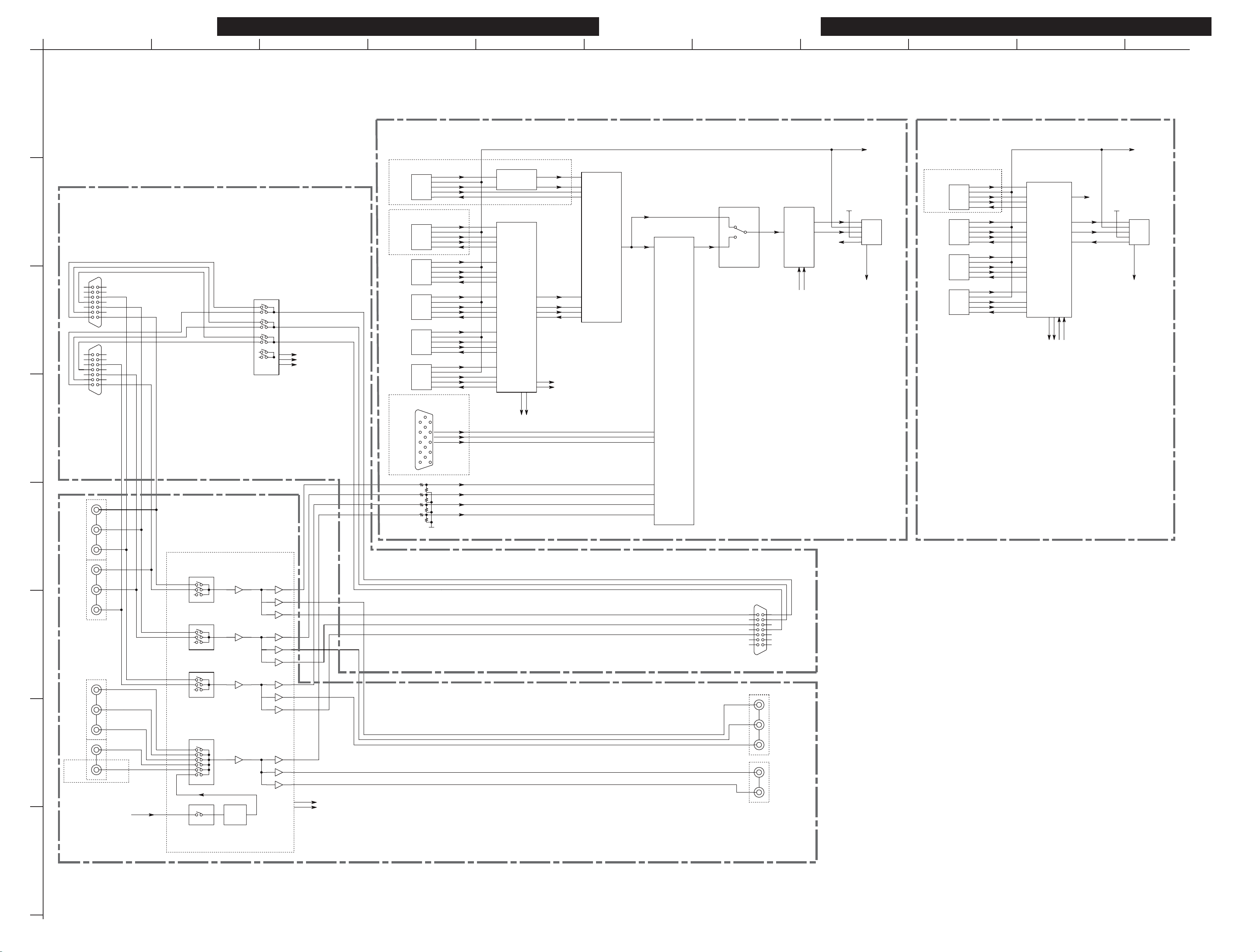
A
SCHEMATIC DIAGRAMS-2
Video BLK Section
1
JAPAN Model only
2
7
14
6
13
12
5
4
11
10
3
9
2
1
3
8
14
13
12
11
10
9
8
D4 VIDEO INPUT
7
6
5
4
3
2
1
BCDEF GH
TC74HC4053
TX-SR578, TX-SR608, HT-R680, HT-R980, TX-SA578, TX-SA608, HT-RC260, DTR-20.2, DTR-30.2
CEC
TX-SR608, TX-SA608, DTR-30.2
TMDS
TMDS
CEC
HDMI
FRONT
TX-SR608, TX-SA608, HT-RC260,
DTR-20.2, DTR-30.2
HDMI IN5
HDMI IN4
HDMI IN3
HDMI IN2
INH
A
B
HDMI IN1
TX-SR608, TX-SA608, HT-RC260,
DTR-20.2, DTR-30.2
CEC
DDC
HP DET
TMDS
CEC
DDC
HP DET
TMDS
CEC
DDC
HP DET
TMDS
CEC
DDC
HP DET
TMDS
CEC
DDC
HP DET
TMDS
CEC
DDC
HP DET
+5V
+5V
+5V
+5V
+5V
+5V
DDC
RPWR
HPD
TMDS
CEC
DDC
RPWR
HPD
TMDS
CEC
DDC
RPWR
HPD
TMDS
CEC
DDC
RPWR
HPD
TMDS
CEC
DDC
RPWR
HPD
TMDS
CEC
DDC
RPWR
HPD
Q8661
TMDS141
Rx Tx
HDMI Buffer
Rx0
Rx1
Q8161
SiI9387
HDMI
Fast Switching
Rx2
Rx3
Rx4
I2S
S/PDIF
TMDS
DDC
TMDS
DDC
Tx
RPWR
HPD
I2C
CEC
Rx3
Rx2
Rx1
Rx0
Q8501
SII9233
HDMI
4Rx
TTL
12bit x3
10bit x3
TTL in TTL out
Q8200
FLI32626
SEQUIOA
Video
Processor
10bit x3
Q8801
Q8802
Q8803
Q8804
TC74VCX162827FT x4
Bus switch
Q8401
12bit x3 DDC
SII9136
TTL Tx
HDMI
Tx
I2S
TMDS
S/PDIF
CEC
HPD
TMDS
CEC
DDC
+5V
HP DET
ARC S/PDIF
HDMI OUT
TX-SR308, TX-SR508, HT-R280, HT-R380, HT-R538, HT-R580, HT-RC230
TX-SR508, HT-R580
HDMI IN4
HDMI IN3
HDMI IN2
HDMI IN1
IJK
CEC
TMDS
TMDS
CEC
CEC
DDC
+5V
HP DET
TMDS
CEC
DDC
+5V
HP DET
TMDS
CEC
DDC
+5V
HP DET
TMDS
CEC
DDC
+5V
HP DET
DDC
RPWR
HPD
TMDS
CEC
DDC
RPWR
HPD
TMDS
CEC
DDC
RPWR
HPD
TMDS
CEC
DDC
RPWR
HPD
Rx Port A
Rx Port B Tx
Q8101
ADV7623
HDMI 4Rx Tx
Rx Port C
Rx Port D
I2S
I2S
S/PDIF
S/PDIF
I2C
TMDS
DDC
HPD
+5V Hot Plug+5V Hot Plug
TMDS
CEC
DDC
HDMI OUT
+5V
HP DET
ARC S/PDIF
4
PC VIDEO IN
Y1
CB1
GND
RGB
VS,HS
I2C
ADINPY
ADINPB
ADINPR
ADINCV
CH,BH,AH
AVS,AHS
I2C
B3P
SV3P
A2P
C4P
5
CR1
Y2
Yin1
CB2
CR2
COMPONENT VIDEO INPUT
Yin2
PBin1
PBin2
6
PRin1
PRin2
DVD
VCR/DVR
CBL/SAT
NJM1326FH2
PY
PB
PR
6dB DRV
DRV6dB
DRV
DRV
DRV6dB
DRV
DRV
DRV
DRV
1
8
2
9
3
10
11
4
5
6
7
12
13
14
Y
CB
D4 OUT
COMPONENT
OUT
7
GAME/TV
AUX1
(FRONT)
COMPOSITE VIDEO INPUT
UPort
Vin2
Vin3
Vin4
Vin5
Vin1
SYin1
CV
YCMIX
6dB
DRV
DRV
DRV
I2C
MUTE
COMPOSITE VIDEO OUTPUT
CR
MONITOR
VCR/DVR
8
TX-SA608/ TX-SR608/ HT-RC260/ DTR-2.02/ DTR-30.2
TX-SA608/ TX-SR608/ HT-RC260/ DTR-2.02/ DTR-30.2
A
SCHEMATIC DIAGRAMS-3c
AUDIO INPUT SECTION
1
2
3
4
5
6
7
8
G
Table:
TX-SR608
DTR-30.2
DC/DD/DF
ADD
A6.4P
U0010
SIR
OHTER
DEL
ONLY:TX-SR608/DTR-30.2 (DC/DD/DF)
G
SIR
ONLY A6
P4001
Rch
TUNER
Lch
J
Rch
TV/CD
Lch
P4002
LIST
L
Rch
L
PC
P4003
Lch
LIST
Rch
GAME
Lch
P4012
LIST
Rch
CBL/SAT
Lch
P4004
LIST
Rch
VCR/DVR
OUT
Lch
Rch
VCR/DVR
Lch
P4005
LIST
Rch
DVD/BD
Lch
TO SD-4c A-3 BAAF-0355
Table:
OHTER
ADD
AMP. ASP
PC BOARD
BAAF-0355
P4000
MSJ-035-22
P4006
GND
SHIELD
SHIELD
L_OUT
AGND
TX
R_OUT
GND
RX
RESET
VIN
2MJ-3516-002
LIST
3
1
2
3
1
2
3
1
2
3
1
2
6
4
5
3
1
2
6
4
5
3
1
2
U0011
1
2
3
JL951B
4
5
NSCT-5P99
(POW AMP Section)
H
TUNER PACK
TX-SA608
DEL
11
10
9
8
7
6
5
4
3
2
1
4
4
4
4
7
7
FLAC1
FLAC2
SEC3_1
SEC3_2
TP4002
C4116
100N
C4215 LIST
C4205 LIST
C4203 102J
LBC2518T2R2M
R4061
1.5K
R4062
1.5K
C4113
NM
R4065
0
R4001
330
R4041
R4002
R4042
330
C4201
NM
R4003
330
R4043
R4004
R4044
330
C4212
NM
R4007
330
R4047
R4008
R4048
330
R4009
330
R4049
R4010
R4050
330
R4013
330
R4053
R4014
R4054
330
R4015
2.2K
R4055
R4016
R4056
2.2K
R4017
330
R4057
R4018
R4058
330
R4019
330
R4059
R4020
R4060
330
C4204
102J
FL/FR uses DVD.and SBL/SBR uses ZONE2 in DVD
-VP PC BOARD
R960
8.2(1/2W)
P5501B NPLG-7P0962
1
RI
L4001
R4000
330
R4021
0
NM
C4114
0
R4235
NM
C4115
J
100K
LIST
C4001
100K
LIST
C4002
100K
221JE
C4007
100K
221JE
C4008
100K
221J
C4003
100K
221J
C4004
100K
221J
C4009
100K
221J
C4010
100K
221J
C4013
100K
221J
C4014
NM
100K
C4015
NM
100K
C4016
100K
221J
C4017
100K
221J
C4018
100K
221JE
C4019
100K
221JE
C4020
Multi ch in for Amp test
-VP (PART 3)
D960
RL1N4003
2 1
D964
NM
R950
8.2(1/2W)
Table:
DTR-2.0.2
DTR-30.2
ADD
BCDEF GH
TO SD-6 K-7
BADG-0364
23456
RI_GND
GND
TUN_L
TUN_R
100K
R4063
152J
C4111
R4064
100K
C4112 152J
(C DIRECT IN)
(SR DIRECT IN)
(SL DIRECT IN)
(FR DIRECT IN)
(FL DIRECT IN)
D961
RL 1N4003
NM
J960
2 1
D965
NM
C960
220/63(VR)
UDZ36B
104J
C950
ZONE2 PREOUT
K
OHTER
DEL
AUDIO ANALOG SIGNAL(TV/CD)
FRONT L
FRONT R
TO SD-9 A-5
7
AGND
3.3(1/2W)
R961
R965
D962
H
R962
8.2K
0
100K
R4068
100K
R4067
DEL:
TX-SA608
TO SD-7 K6
BAVD-0375
BAVD-0389
NSCT-3P874
JL503A
A
2SC2235-O
Q960
R963
8.2K
NM
D963
47/50(VR)
C961
1
Z2 L-CH
Except A6
BAPS-0356
33K
104Z
C962
R964
2
3
GND
Z2 R-CH
Table:
ADD
BAETC-0365
(U-PORT)
NSCT-5P876
JL502A
432
5
GND
U_PORT_L
+3.3VMPU
FL_AC1
-VP
FL_AC2
+3.3VMPU
L
TO SD-6 K-7 BADG-0364
1
1
2345678
-15V
+15V
U_PORT_R
R4202
R4080
100K
R4081
100K
JL953B
1
2
3
4
5
C4061
K
DAC_FR
LTAD
RTAD
0
47/50
C4060
47/50
R4082 100K
5.1K
R4305
R42250R4306
NPLG-5P590
(Display Section Section)
TO SD-10b B-2 BADIS-0388
TO SD-10a C-2 BADIS-0381
PC INPUT
HT-RC260OHTER
DEL
P5502B NPLG-15P0970
DAC_SW
DAC_CT
DAC_FL
81
80
N.C.
79
IN-L9
78
IN-R9
77
N.C.
76
INLA/RECL1
75
INRA/RECR1
74
N.C.
73
IN-L8
72
IN-R8
71
IN-L7
70
IN-R7
69
IN-L6
68
IN-R6
67
IN-L5
66
IN-R5
65
IN-L4
64
IN-R4
63
IN-L3
62
IN-R3
61
IN-L2
60
IN-R2
59
IN-L1
58
IN-R1
57
N.C.
56
AGND
55
ADCR
54
ADCL
53
N.C.
52
AVEE
51
MUTE
50
R4088 10K
5.1K
9
12
10
11
131415
DAC_SL
DAC_SR
DAC_SBR
DAC_SBL
AUX_L
AUX_R
MICOUT
C407147/50
R4078
47K
R4079
47K
R4069
100K
93
91
88
85
83
82
49
10K
R4087
84
TUN
TV/CD
GAME
PC
CBL/SAT
VCR
DVD
CLOCK
DATA
DGND
SUBR
47
48
Z2L_CH
R4089 0
87
86
N.C.
INL11/RECL5
INR11/RECR5
INLB/RECL2
INRB/RECR2
SBLC-IN44SBRC-IN
SUBL
45
46
47/50
C4086
Z2R_CH
0
R4234
90
89
N.C.
N.C.
RECR3
INL10/RECL4
INR10/RECR4
R2A15218FP
Q4001
(Botom view)
FL-IN2
FR-IN2
SR-IN2
42
40
43
41
C4085 47/50
47/25
C4209
220K
R4189
220K
R4190
47/25
C4210
92
N.C.
RECL3
SL-IN2
SW-IN2
39
R4307 5.1K
FL-IN1
TRER
C-IN2
38
NJM4580M
DMIXR
R4090
C4090 101J
R4094
R4095
C4091 101J
R4098
NJM4580M
DMIXL
Downmix
FL/FR -12dB
SW +3.5dB
K
Z2_OUT_R
Z2_OUT_L
7
TO SD-13 F-5 NAAR-0411
TO PART 13(Zone Volume/RS232C)
C407047/50
95
94
FR-IN1
BASS-R2
SBR-IN2
37
36
+15V
C407747/50
C407247/50
97
96
C-IN1
SL-IN1
SW-IN1
SBL-IN1
SBR-IN1
N.C.
BASS-R1
N.C.
SBL-IN2
35
34
223J
C4064
1
Q4003A
12K
10K
10K
12K
7
Q4003B
Z2_LCH_IN
Z2_RCH_IN
JL606ANSCT-7P878
C407447/50
98
SR-IN1
SBL-OUT
SBR-OUT
SR-OUT
SW-OUT
FR-OUT
BASS_L1
BASS-L2
33
823J
C4063
4
8
-15V
GND
1
23456
C407347/50
C407647/50
100
99
N.C.
SBLC
AGND
SBRC
AGND
SLC
SL-OUT
AGND
SRC
N.C.
SWC
AGND
C-OUT
AGND
FLC
FL-OUT
AGND
FRC
N.C.
TREL
N.C.
AVCC
32
31
C4062
R4086
1.8K
R4232
3
R4091
2
R4092
R4096
5
6
CC
0
C407547/50
474J
22K
330
330
R4192
R4099
22K
1
2
3
4
5
6
7
8
9
10
11
12
13
14
15
16
17
18
19
20
21
22
23
24
25
26
27
28
29
30
220K
R4195
R4196
R4193
R4194
C4056
C4055
C4054
C4053
C4057
C4052
C4051
C4050
C4065 474J
C4066 823J
C4067 223J
470/16
C4174
C4175
470/16
R4093
3.3K
R4097
3.3K
TO SD-20 D-2
BAETC-0366
P5506B NPLG-5P0960
12345
DAC_FR
VLSC_FR
DAC_FL
0
R4201
220K
220K
220K
220K
47/25
47/25
47/25
47/25
47/25
220/10
220/10
220/10
R4085
1.8K
*
Q4184
*
2SC2235
D4172
220/25
MTZJ7.5B
C4184
D4171
220/25
C4185
MTZJ7.5B
*
2SA965
Q4185
*
Table:
R4001-02
R4041-42
R4200-01
C4001-02
P4001
P4002
P5506B-08B
VLSC_FL
R4200
1W
R4174
100
R4184
1K
C4186
220/25
C4187
220/25
1K
R4185
1W
R4175
100
J
0
22
R4167
C4167
220/25
220/25
C4166
22
R4166
TX-SA608
TO SD-20 D-1
BAETC-0366
P5507A NPLG-3P0960
1
1234
P5508B
ONLY:
J
TX-SA608
OHTER
ADD
ADD
DEL
221J 152J
ADD
DEL
ADD
DEL
DEL
ADD
DEL
ADD
DEL
TX-SR608
HT-RC260
Table:
DD/DC/DF
B
MP/MB/MO
MA/MQ/MR
R4210
R4211
R4180
R4182
TO SD-6 K-6
BADG-0364
P5503B NPLG-9P0964
3
1
4
5
8
2
3
0
0
JL408A
R4224
R4223
1
-15V
2
+15V
VOLDATA
47/50
C4130
R4220
2 1
2 1
VOLCLK
0
D4305
D4304
9
6
7
PROTECT
SEC1H
AMUT
VOLH
IPROTECT
0
R4221
220
R4130
3
2
221J
C4131
R4131
47K
R4132
15K
5
6
+/- 15V Supply
Q4170 78M15
3
1
O
I
G
2
220/25
C4172
C4173
220/25
1
3
G
O2I
Q4171 79M15
3
4
Q4170A RAD-196
2
1
4
Q4130A
R4133
Q4130B
8
R4180
R4181
R4182
NJM4580M
R4134
C4132 103J
1.2K
NJM4580M
SR_OUT
SL_OUT
FR_OUT
FL_OUT
C4170
C4171
1
10K
7
C_OUT
10/50
10/50
TX-SA608
DEL
ADD
ADD
ADD
ADD
DEL
DEL
DEL
TO SD-6 K-6 BADG-0364
P5504B NPLG-7P0962
3
1
2
4
SR_RST
SBZ2MUT
SR_RXD
Z2MUT
220K
220K
220K
B
0
R4210
R4211
SW_OUT
Subwoofer
AV=20dB
SBR_OUT
SBL_OUT
2W
R4170
3.3
R4172
NM
2W
2W
R4171
8.2
2W
R4173
NM
JJ
567
SR_TXD
SBRELAY
0
R4022
R4222
C
47/50
C4104
C4103
47/50
47/50
C4101
C4100
47/50
PRRLF
0
0
220K
220K
Table:
C4301
C4302
-25V
NM
C4023
C4107
47/50
47/50
C4106
C4105
47/50
R4104
Q4103
R4103
47/50
C4102
1000/35
470/35
DTR-20.2
DTR-30.2
DD/MA
DEL
ADD
ADD
ADD
R4023
0
RN1441
Q4104
LIST
R4114
R4113
LIST
RN1441
220K
R4101
LIST
R4111
R4110
LIST
220K
R4100
C4108
47/50
C4109
47/50
A
D4301
1 2
RL1N4003
1 2
D4302
AMUT
SB2Z2MUT
SB2Z2MUT
Z2MUT/PRE OUT RELAY
NM
C4024
270
sw
RN1441
R4117
Q4107
220K
R4107
Q4106
220K
LIST
R4106
R4116
RN1441
SBR
SBL
Q4105
R4115
LIST
220K
R4105
SR
SL
0
R4226
Q4101
FR
RN1441
FL
Q4100
RN1441
LIST
R4112
220K
R4102
CEN
2.2K
R4118
220K
R4108
220K
R4109
2.2K
R4119
TX-SA608
DEL
M
R4160
0.22 or 2.2 1W
D4300
1 2
1 2
D4303
0.22 or 2.2 1W
R4161
M
RN1441
0
R4236
RN1441
Q4102
Q4108
RN1441
RN1441
Q4109
A
OTHER
ADD
334J
C4300
2.2
0
R4024
100
R4127
LIST
R4126
R4125
LIST
LIST
R4124
R4123
LIST
LIST
R4121
R4120
LIST
LIST
R4122
GND_S1
+24V
S1L-
GND_AMP
S1L+
1W
C6076-77
C6086-87
P6602
JL604A
Table
R4110-14
R4115-16
R4120-24
R4125-26
Q4105-06
Q4110-14
NM
C4025
Q4115-16
RN1441
Q4117
LIST
Q4116
LIST
Q4115
LIST
Q4114
Q4113
LIST
LIST
Q4111
Q4110
LIST
LIST
Q4112
TO SD-4c A-4
TO SD-4c B-8
Table
F
TX-SA608
DTR-30.2
C
JJ/DD/MA
BAAF-0355
BAAF-0355
TX-SR608
HT-RC260
DC/DD/DF
DEL
DEL
ADD
ADD
OTHER
DEL
DEL
DEL
DEL
TO SD-4c A-5 BAAF-0355
( MAIN AMP SECTION)
DTR-20.1
120 2.2K
120
100
100
ADD
ADD
Table:
DD
2.2K
270
100
ADD
ADDADD
ADD
M
0
R4227
OTHER
2.2K
ADD
DEL
DEL
TX-SR608/ DTR-30.2
MP/MB/MO/MA/MQ/MR
0.22(1W)
VOLH
SEC1H
IPROTECT
VPROTECT
00
0
Q4201
RN1402
0
R4231
0
R4230
0
R4229
0
R4228
OHTER
2.2(1W)
Q4200
RN1402
R4168
22
RL4200
8
10
5
3
12
PREOUT RELAY
J4002
J4000
J4003
J4001
R4208
R4209
8
10
5
3
12 1
D4201 KDS4148U
C4211 103K
PREOUT RELAY
1
JL408B
IJK
Table
D
J4000
J4001
J4002
J4003
J4005
R4168
R4128
R4208
R4209
C4200
C4211
D4200
D4201
Q4200
Q4201
RL4200
RL4201
9
4
1
0
RL4201
0
TX-SR608
HT-RC260
DC/DD/DF
MP/MB/MO
MA/MQ/MR
ADD
ADD
DEL
ADD
ADD
DEL
DEL
DEL
DEL
DEL
DEL
DEL
DEL
DEL
DEL
DEL
DEL
TX-SA608
JJ
DEL
DEL DEL
ADD
DEL DEL DEL
DEL
ADD
DEL
ADD
ADD
DEL
ADD
DEL
ADD
DEL
ADD
DEL
Zone2 SPK or High or Wide SPK Leber
NSCT-5P896
JL604A
TO SD-8 F-2 BATRM-0369
D
D4200
KDS4148U
C4200
103K
D4217
D4207
1 2
2 1
J4005
9
4
D4208
D4218
2 1
1 2
R4128
22
DTR-30.2
DTR-20.2
DD
DD/MA
DEL
DEL
DEL
ADD
ADD
ADD
DEL
ADD
DEL
ADD
DEL
DEL
ADD
ADDADD
DEL
DEL
ADD
DEL
ADD
ADD
DEL
ADD
DEL
ADD
DEL
ADD
DEL
ADD
DEL
DEL
ADD
ONLY: TX-SR608(DD/DF)
HT-RC260(MDD)
GND_E
Z2RE
5
4
103J
C6086
Z2LE
3
Z2R
2
1
C6087
Z2L
R4031
LIST
221J
C4031
R4071
LIST
R4030
221J
R4070
C4030
C4207221J
R4028
22K
221J
R4077
C4027
LIST
R4032
LIST
R4072
C4032
C4213LIST
R4034
LIST
220K
R4074
C4034
220K
221J
R4033
R4073
C4033
R4036
220K
LIST
R4076
C4036
R4035
LIST
220K
R4075
C4035
C4214LIST
C4208LIST
C4206
LIST
LIST
C4037
103J
LIST
LIST
100
LIST
LIST
LIST
LIST
LIST
R4029
LIST
R4027
GND
C6077
LIST
SBL
SL
102J
3
SBR
G
SR
G
R
G
C
G
L
G
G
4
4
4
4
C6076
102J
3
2
3
2
3
2
3
2
2
10
11
12
13
1
1
1
1
1
2
3
4
5
6
7
8
9
1
R4030.31
R4070.71
R4032
R4033.34
R4072
R4073.74
R4035.36
R4075.76
R4027
R4029
C4032
C4033.34
C4035.36
C4037
C4206
P4007
P4008
P4009
P4010
P4011
5
4
2
3
1
6
LIST
LIST
1
TX-SR608
HT-RC260
DC/DD/DF
MP/MB/MO
MA/MQ/MR
330
2.2k
100
DEL
22k
DEL
DEL
DEL
DEL
DEL
221J
DEL
DEL
DEL
DEL
ADD
DEL
DEL
DEL
ADD
L
TX-SA608
JJ
100
220K
100
100
220K
220K
100
220K
22k
100
221J
221J
221J
221J
102J
ADD
ADD
DEL
ADD
F
NTM-4PDML422
Table: E
E
P6602
R
NOTE
DEL:Deleton
ADD:Addton
DC Canadian model
DD USA model
DF Taiwanese model
MO Saudi Arabian model
MQ Hong kong model
PA Australian model
PB
MB U.K. model
PP
MP CE(European) country model
MR Chinese model
JJ Japanese model
FRONT R
ZONE2/HIGH/WIDE/RIGHT
P4007
LIST
FRONT L
ZONE2/HIGH/WIDE/LIFT
PRE_C/SW
SW
P4011
LIST
C/SW2
SR
P4008
LIST
SL
PRE_SURR
SBR/HIGH/WIDE R
SW2
ONLY:TX-SR608(DD)
TR-20.2/HT-RC260
CENTER
ONLY:TX-SA608/DTR-30.2
P4009
SBL/HIGH/WIDE L
PRE OUT
PRE_SURRBK
ONLY:TX-SA608/DTR-30.2
SW2(ONLY:TX-SA608/DTR-30.2)
P4010
P6600B
TO SD-4c E-8 BAAF-0355
(POW AMP SECTION)
TO SD-4c F-8 BAAF-0355
(POW AMP SECTION)
P5505B
DTR-30.2
DTR-20.2
DD/MA
DD
100
DEL
DEL
220K
100
100
DEL
100
22k
220K
220K
DEL
100
100
220K
220K
22k
DEL
DEL
DEL
DEL
DEL
DEL
DEL
ADD
ADD
221J
221J
DEL
100
221J
221J
221J
221J
102J
ADD
ADD
DEL
ADD
DELDEL
E
FRONT PRE-OUT:
TX-SA608/DTR-30.2
Zone2 Line OUT:
TX-SR608/HT-RC260
E
E
E

TX-SA608/ TX-SR608/ HT-RC260/ RTR-20.2/ DTR-30.2
TX-SA608/ TX-SR608/ HT-RC260/ DTR-20.2/ DTR-30.2
A
SCHEMATIC DIAGRAMS-4c
MAIN AMP (Input Stage) SECTION
1
HT-RC260
DTR-30.2
2SC4468
2SC4468
2SC4468
2SA1695
2SA1695
2SA1695
TX-SA608
2SC5242
2SC5242
2SC5242
2SA1962
2SA1962
2SA1962
TX-SR608
ONLY:PP
2SC5242
2SC5242
2SC5242
2SA1962
2SA1962
2SA1962
TRANS FIX PC BOARD
345
SEC3_1
SEC3_2
P954
10K
R6702
C6703
Q6703
2SA1163-BL
D6703
10K
R6712
C6713
Q6713
2SA1163-BL
D6713
TO B-4
P6903B
YEW
TO B-4
GRN
TO SD-7 C-8
BAVD-0382
BAVD-0389
2
1
SEC2_1
P956
P955
104Z
2SC2712-GR
47K
R6704
R6706
UDZS3.3B
104Z
47K
R6714
R6716
UDZS3.3B
1
1
P6904B
TP6005
TO SD-4c A-7
BAAF-0355
Q6702
220K
220K
S1H+
S1H-
P951
GND_S1
+24V
VOLH
SEC1H
VPROTECT
IPROTECT
TP6007
TO SD-3c A-3
BAAF-0356
JL951A
1
FLAC1
TP6004
P952
P953
R6701
22K
AC_S1L+
N.C
C6704
C6714
2
FLAC2
1/50
1/50
DTR-20.2
U0012
THERMAL SENSER PC BOARD
NSCT-3P898
JL952A
3
SEC2_2
TP6001
P6903B(YEW)
P957
1
(YEW)
33K
R6708
Q6701
2SC2712-GR
21
D6702
KDS4148U
C6706
10/50
8.2
(1W)
R6197
*
S1L+
1
SN5051
F6901
12A 250V
2
3
4
5
6
7
TX-SR608
Power Tr
EXCEPT:PP
Q6050-52
Q6053-54
Q6055-56
Q6060-62
Q6063-64
Q6065-66
U0012
BAETC-0359
P950
TO SD-3c G-7
BAAF0355
(Audio Input
Section)
TO SD-3c I-2
BAAF0355
(Audio Input
Section)
NSCT-5P896
1
2
TO B-4
3
4
5
2SC4468
2SC4468
2SC4468
2SA1695
2SA1695
2SA1695
NSCT-5P898
BCDEF GH
AUDIO ANALOG SIGNAL
FRONT L
FRONT R
2SC4468
2SC4468
--
2SA1695
2SA1695
--
21
Q6380A
RETAINER
BAETC-0357
TO SD-4c A-8 BAAF-0355
4
321
5
TP6002
TP6006
AC_S1L+_
P6900B(BLK)
P959
P958
1
1
TO SD-4c A-7
BAAF-0355
21
D6701
KDS4148U
NM
C6701
100/25
R6721
4.7K
5.6K
R6710
D6704
R6709
UDZS3.3B
R6902
1K
47K
R6903
Q6707
2SC2712-GR
12
102J
C6911
D6902
1SS352
104J
C6915
LM61CIZ
1
C6630
NM
JL501A
NSCT-3P874
TO SD-6 K-4
BADG-0364
NSCT-5P896
JL954A
TP6003
AC_S1L-_
P6904B(GRN)
P960
P961
1
1
TO SD-4c D-7
BAAF-0355
(GRN)(BLK)
RL6902
4
1
3
2
5
NRL-1P10A-DC12-196
5
2
3
1
4
RL6901
NRL-1P10A-DC12-196
C6631
NM
Q6380
G
2
+3.3VMPU
GNDDG2
2
1
3
V
O
THERMAL
3
TO A-8
C6912
334J/100V
C6913
334J/100V
U0010
BAAF-0355
D10XB60H
3
D6901
4
2
AMP. ASP PC BOARD BAAF-0355
FRONT(L) CH
GND_L
L_IN
P6000B
NPLG-9P0964
(ANP CLASS_A)
TO SD-5 F-4 BACLA-0362
FRONT(R) CH
GND_R
R_IN
P6001B
(ANP CLASS_A)
TO SD-5 F-5 BACLA-0362
CENTER CH
GND_C
C_IN
P6002B
(ANP CLASS_A)
TO SD-5 F-7 BACLA-0362
P6901A
GND_AMP
1
3
D6901A
RAD-196
2
+B1H_B
4
BLK
1
-B1H_B
TO B-4
P6900B
GRAY
1
C6901
LIST
C6902
P6902A
1
+
LIST
+
10000u/69V
1
10000u/69V
TO F-1
TO F-1
WHITE
P6011A
+B1L
9
8
7
6
5
+BL
4
+BL2
3
-BL2
2
TRIML
1
+B1R
9
8
7
6
5
+BR
4
+BR2
3
-BR2
2
TRIMR
1
NPLG-9P0964
+B1C
9
8
7
6
5
+BC
4
+BC2
3
-BC2
2
TRIMC
1
NPLG-9P0964
-B1L
AV=29dB
-B1R
AV=29dB
-B1C
*
R6030
*
R6000
*
R6010
*
R6031
*
R6001
*
R6011
*
R6032
*
R6002
*
R6012
2.2K
4.7K
3.3K
2.2K
4.7K
3.3K
2.2K
4.7K
3.3K
0.8V
-0.4V
-0.4V
0.8V
0.8V
-0.4V
NFL
NFR
Q6000
2SC1740S-S
Q6001
2SC1740S-S
Q6002
2SC1740S-S
54.5V
P6080
NPLG-2P29
ID+
ID-
(NH)
-54.5V
54.5V
P6081
NPLG-2P29
ID+
ID-
(NH)
-54.5V
54.5V
P6082
NPLG-2P29
ID+
ID-
(NH)
-54.5V
Q6050
2SC4468
2SC5242
R6140
56K
R6100
0.22(5W)
2
1
Q6060
2SA1695
2SA1962
D6000
KDS4148U
Q6051
2SC4468
2SC5242
R6141
56K
R6101
0.22(5W)
2
1
Q6061
2SA1695
2SA1962
D6001
KDS4148U
Q6052
2SC4468
2SC5242
R6142
56K
R6102
0.22(5W)
2
1
0
R6301
Q6062
2SA1695
2SA1962
D6002
KDS4148U
10K
R6150
10K
R6151
12
12
10K
12
R6170
47K
R6171
47K
R6172
47K
R6180
47K
R6181
47K
R6152
R6182
47K
Q6070
2SC2229
C6050
Q6071
2SC2229
C6051
Q6072
2SC2229
C6052
103J
1 2
103J
1 2
103J
1 2
R6190
D6010
R6191
D6011
R6192
D6012
NM
NM
NM
NM
NM
NM
VPRO
VOLH
VPRO
VOLH
VPRO
VOLH
R6160
SPL
33K
R6161
SPR
33K
R6162
WHITE
GRAY
TO D-7
TO D-8
#18
P6901B
-B +B
33K
1
1
P6010B
L
PCB HOLD
P6902B
#18
+B1SL
SURROUND(L) CH
GND_SL
SL_IN
(ANP CLASS_A)
TO SD-5 J-2 BACLA-0362
SURROUND(SR) CH
GND_SR
SR_IN
(ANP CLASS_A)
TO SD-5 J-4 BACLA-0362
EXCEPT: DTR-20.2
SURROUND BACK(L) CH
GND_SBL
SBL_IN
(ANP CLASS_A)
TO SD-5 J-5 BACLA-0362
EXCEPT: DTR-20.2
SURROUND BACK(R) CH
GND_SBR
SBR_IN
R
PCB HOLD
1234
P6009B
1234
1234
1234
1234
P6007B
P6008B
P6012B
VOLH
IPRO
VPRO
(ANP CLASS_A)
TO SD-5 J-7 BACLA-0362
NPLG-9P0964
9
8
7
6
5
4
3
2
1
P6003B
NPLG-9P0964
9
8
7
6
5
4
3
2
1
P6004B
NPLG-9P0964
9
8
7
6
5
4
3
2
1
P6005B
NPLG-9P0964
9
8
7
6
5
4
3
2
1
P6006B
AV=29dBAV=29dB
+BSL
+BSL2
-BSL2
TRIMSL
-B1SL
+B1SR
AV=29dB
+BSR
+BSR2
-BSR2
TRIMSR
-B1SR
+B1SBL
AV=29dB
+BSBL
+BSBL2
-BSBL2
TRIMSBL
-B1SBL
+B1SBR
AV=29dB
+BSBR
+BSBR2
-BSBR2
TRIMBSR
-B1SBR
*
R6033
*
R6003
*
R6013
*
R6034
*
R6004
*
R6014
*
R6035
*
R6005
*
R6015
*
R6036
*
R6006
*
R6016
2.2K
4.7K
3.3K
2.2K
4.7K
3.3K
2.2K
4.7K
3.3K
NFSBR
2.2K
4.7K
3.3K
IJK
54.5V
Q6053
NFSR
NFSBL SPSBLNFC SPC
NFSL
0.8V
-0.4V
0.8V
-0.4V
0.8V
-0.4V
0.8V
-0.4V
Q6003
2SC1740S-S
Q6004
2SC1740S-S
Q6005
2SC1740S-S
Q6006
2SC1740S-S
P6083
NPLG-2P29
ID+
ID-
(NH)
-54.5V
54.5V
P6084
NPLG-2P29
ID+
ID-
(NH)
-54.5V
54.5V
P6085
NPLG-2P29
ID+
ID-
(NH)
0
R6305
-54.5V
54.5V
P6086
NPLG-2P29
ID+
ID-
(NH)
-54.5V
2SC4468
2SC5242
R6143
R6103
0.22(5W)
2
1
Q6063
2SA1695
2SA1962
KDS4148U
Q6054
2SC4468
2SC5242
R6144
R6104
0.22(5W)
2
1
Q6064
2SA1695
2SA1962
KDS4148U
Q6055
2SC4468
2SC5242
R6145
R6105
0.22(5W)
2
1
Q6065
2SA1695
2SA1962
KDS4148U
Q6056
2SC4468
2SC5242
R6146
R6106
0.22(5W)
2
1
Q6066
2SA1695
2SA1962
KDS4148U
56K
D6003
56K
D6004
56K
D6005
56K
D6006
10K
R6153
10K
R6154
10K
R6155
10K
R6156
12
12
12
12
R6173
47K
R6174
47K
R6175
47K
R6176
47K
R6183
47K
R6184
47K
R6185
47K
R6186
47K
Q6073
2SC2229
103J
C6053
Q6074
2SC2229
103J
C6054
Q6075
2SC2229
103J
C6055
Q6076
2SC2229
103J
C6056
33K
R6163
SPSL
NM
R6193
NM
D6013
1 2
VPRO
VOLH
33K
R6164
SPSR
NM
R6194
NM
D6014
1 2
VPRO
VOLH
33K
R6165
NM
R6195
NM
D6015
1 2
VPRO
VOLH
33K
R6166
SPSBR
NM
R6196
NM
D6016
1 2
VPRO
VOLH
8
JL954B
TO SD-4c B-3
BAETC-0359
AC_S1L-
SN5051
S1L-
1
F6902
S1L+
TO SD-3c G-7 BAAF-0355
(Audio Input Section)
104J
S1L-
GND AMP
C6916
(PART 3)
SLELECERESRE
SBLE
TO SD-8 D-5
BATRM-0368
(SP TRM Section)
JL620A
SPSBLE
SPSLE
SPLE
SPCE
SBRE
1234567
JL603A
TO SD-8 F-2
BATRM-0368
(SP TRM Section)
SPRE
SPSBRE
SPSRE
+24V
GNDRL
123456789
R_IN
SBR_IN
SR_IN
C_IN
GGG
P6600A NSAS-26P1775
TO SD-3c J-7
BAAF-0355
(Audio Input Section)
1
G
G
SBL_IN
L_IN
SL_IN
G
P5505A
13121110987654321
TO SD-3c J-7
BAAF-0355
(Audio Input Section)
SPSL
JL600A
TO PART 8(SP TRM)
7654321
SPSBR
SPSR
SPR
SPC
SPL
SPSBL
TO BATRM-0368
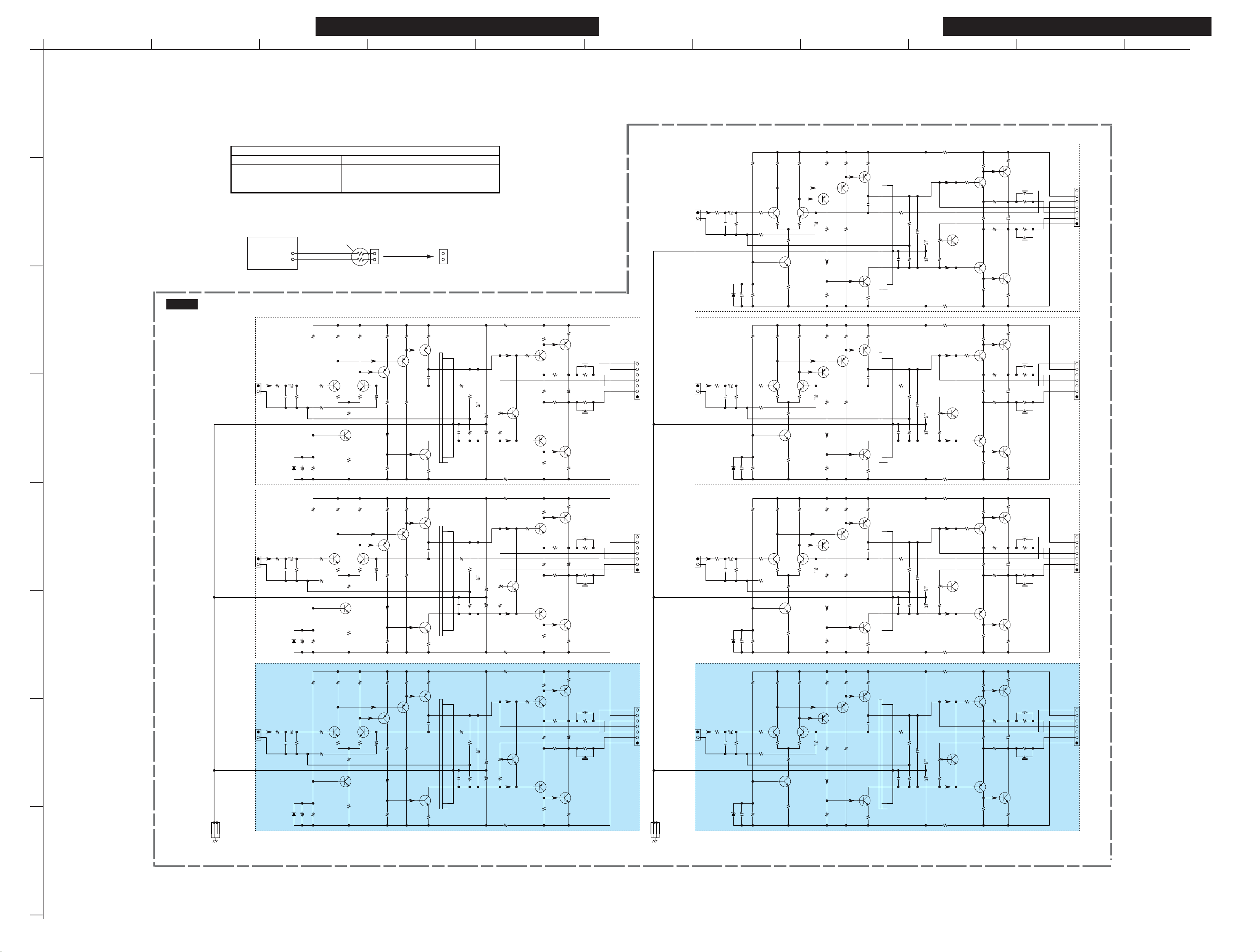
TX-SA608/ TX-SR608/ HT-RC260/ DTR-20.2/ DTR-30.2
TX-SA608/ TX-SR608/ HT-RC260/ DTR-20.2/ DTR-30.2
A
SCHEMATIC DIAGRAMS-5
MAIN AMP (Input Stage) SECTION
1
2
3
4
5
6
7
IDLING CURRENT ADJUSTMENT
U0020
BCDEF GH
a.
Set the voltages at P6080䌾6086 to 1.5mV by adjusting R6040䌾6046, under the condition of
no input and no load, immediately after POWER ON.
c.
4䌾6䇭minutes of heat running.
Re-adjust by following procedure.
d.
All
Below 7mV
Return to 'c' ,after it adjusted to 7mV.
Between 7䌾8mV 8mV
Between 8䌾10mV Leave it as it is.
Over 10mV 10mV
*Set R6040䌾6046 to minimum position before POWER ON.
*Equip series 1/4W 100-ohm resisters near the terminal respectively
in the each poles of the jig used for P6080-6086 terminals.
DC voltmeter
100 ohms
(1/4 watt)
Jig terminal
AMP. (INPUT) PC BOARD BACLA-0362
33K
R5010
C5020
MTZJ5.6B
33K
R5013
C5023
MTZJ5.6B
33K
R5015
C5025
MTZJ5.6B
63.9V[56.6V]
100K
R5090
R5020
R5040
100K
10/50
R5100
63.9V[56.6V]
100K
R5093
R5023
R5043
100K
10/50
R5103
63.9V[56.6V]
100K
R5095
R5025
R5045
100K
10/50
R5105
R5110
330
R5300
1K
-48.2V
-63.9V[-56.6V]
R5113
330
R5303
1K
-48.2V
-63.9V[-56.6V]
R5115
330
R5305
1K
-48.2V
-63.9V[-56.6V]
2.2K
Q5010
Q5000
2SC2240-BL
330
-0.9V
R5050
2.7K
R5060
2.2K
Q5013
Q5003
2SC2240-BL
330
-0.9V
R5053
2.7K
R5063
2.2K
Q5015
Q5005
2SC2240-BL
330
-0.9V
R5055
2.7K
R5065
2.2K
R5120
62.1V[54.8V]
2SC2240-BL
330
R5310
5.6K
Q5050
2SC2240-BL
2.2K
R5123
62.1V[54.8V]
2SC2240-BL
330
R5313
5.6K
Q5053
2SC2240-BL
2.2K
R5125
62.1V[54.8V]
2SC2240-BL
330
R5315
5.6K
Q5055
2SC2240-BL
GND_DecupL
2341
P6007A
FRONT(L) CH
R5000
1.5K
C5010
47/50
C5000
D5000
101J
7
8
P6000A:B
SURROUND
(L) CH
R5003
1.5K
C5013
47/50
C5003
D5003
101J
7
8
P6003A:B
SURROUND
BACK(L) CH
EXCEPT
: DTR-20.2
R5005
1.5K
C5015
47/50
C5005
D5005
101J
7
8
P6005A:B
C5040
C5043
C5045
R5210
470/10
R5150
R5170
R5213
470/10
R5153
R5173
R5215
470/10
R5155
R5175
820
(1/4W)
Q5040
2SA949Y
-61.3V[-54.0V]
1K
(1/4W)
-62.7V[-55.5V]
820
(1/4W)
820
(1/4W)
Q5043
2SA949Y
-61.3V[-54.0V]
1K
(1/4W)
-62.7V[-55.5V]
820
(1/4W)
820
(1/4W)
Q5045
2SA949Y
-61.3V[-54.0V]
1K
(1/4W)
-62.7V[-55.5V]
820
(1/4W)
820
R5140
52.3V
Q5030
-62.4V[-55.1V]
1K
R5080
820
R5143
52.3V
Q5033
-62.4V[-55.1V]
1K
R5083
820
(1/4W)
R5145
52.3V
Q5035
-62.4V[-55.1V]
1K
R5085
(1/4W)
2SA949Y
0V
(1/4W)
Q5070
(1/4W)
2SA949Y
0V
(1/4W)
Q5073
2SA949Y
0V
(1/4W)
R5160
R5220
R5163
R5223
R5165
R5225
Test point
ID+
ID-
120
(1/4W)
Q5060
1
2SA949Y
1.2V
040D
C5080
Q5030A
-1.2V
2
3
2SC2229Y
120
(1/4W)
120
(1/4W)
Q5063
1
2SA949Y
1.2V
040D
C5083
Q5033A
-1.2V
2
3
2SC2229Y
120
(1/4W)
120
(1/4W)
Q5065
1
2SA949Y
1.2V
040D
C5085
Q5035A
-1.2V
2
Q5075
3
2SC2229Y
120
(1/4W)
R5030
C5090
R5033
C5093
R5035
33K
C5095
33K
101J
33K
101J
101J
R5200
R5130
R5203
R5133
R5205
R5135
18K
C5050
18K
18K
C5053
18K
18K
C5055
18K
47/50
C5100
C5110
47/50
C5103
C5113
+BSBL
47/50
C5105
C5115
+BL
22/100
22/100
+BSL
22/100
22/100
22/100
22/100
R5180
(1/4W)
3
R5440
1
R5450
R5190
R5183
(1/4W)
3
R5443
1
R5453
R5193
R5185
(1/4W)
3
R5445
1
R5455
R5195
-0.4V
-0.5V
-0.4V
-0.5V
-0.4V
-0.5V
33K
R5012
C5022
MTZJ5.6B
63.9V[56.6V]
R5092
R5022
R5042
10/50
R5102
100K
330
1K
-48.2V
100K
R5112
R5302
2.2K
Q5002
2SC2240-BL
330
-0.9V
5.6K
R5052
2.7K
R5062
2.2K
R5122
62.1V[54.8V]
2SC2240-BL
Q5012
330
R5312
Q5052
2SC2240-BL
C5042
R5212
470/10
R5152
R5172
820
(1/4W)
Q5042
2SA949Y
-61.3V[-54.0V]
1K
(1/4W)
-62.7V[-55.5V]
820
(1/4W)
820
(1/4W)
R5142
52.3V
Q5032
-62.4V[-55.1V]
1K
R5082
2SA949Y
0V
(1/4W)
Q5072
R5162
1.2V
C5082
-1.2V
R5222
120
(1/4W)
Q5062
2SA949Y
040D
Q5032A
2SC2229Y
120
(1/4W)
1
R5032
33K
18K
R5202
C5052
18K
101J
R5132
C5092
2
3
CENTER CH
R5002
C5012
7
8
1.5K
47/50
101J
P6002A:B
C5002
D5002
-63.9V[-56.6V]
10
2
2K
3.9K
(1/4W)
10
10
2
2K
3.9K
(1/4W)
10
10
2
2K
3.9K
(1/4W)
10
+B1L
R5420
10
(1/4W)
Q5410
2SC1740S-S
+B1SL
R5423
10
(1/4W)
Q5413
2SC1740S-S
+B1SBL
R5425
10
(1/4W)
Q5415
2SC1740S-S
R5270
R5470
R5280
R5273
R5473
R5283
R5275
R5475
R5285
120
(1/4W)
Q5430
R5350
18
(1/4W)
82
R5360
18
(1/4W)
2SA949Y
Q5440
120
(1/4W)
-B1L
120
(1/4W)
Q5433
2SC2229Y
R5353
18
(1/4W)
82
R5363
18
(1/4W)
Q5443
120
(1/4W)
-B1SL
120
(1/4W)
Q5435
R5355
18
(1/4W)
82
R5365
18
(1/4W)
Q5445
120
(1/4W)
-B1SBL
2SC2229Y
(1/4W)
(1/4W)
2SA949Y
2SC2229Y
(1/4W)
2SA949Y
R5370
0.6V
C5440
-0.6V
R5380
R5373
0.6V
C5443
-0.6V
R5383
R5375
0.6V
C5445
-0.6V
R5385
2.2
Q5250
22/50
Q5260
2.2
(1/4W)
2.2
Q5253
22/50
Q5263
2.2
2.2
(1/4W)
Q5255
22/50
Q5265
2.2
(1/4W)
(1/4W)
2SA1930
L5400
R5480
10
R5490
10
L5410
2SC5171
(1/4W)
2SA1930
L5403
R5483
10
R5493
10
L5413
2SC5171
(1/4W)
2SA1930
L5405
R5485
10
R5495
10
L5415
2SC5171
NFL
+B1L
-B1L
+BL
+BL2
-BL2
TRIML
NFSL
+B1SL
-B1SL
+BSL
+BSL2
-BSL2
TRIMSL
NFSBL
+B1SBL
-B1SBL
+BSBL
+BSBL2
-BSBL2
TRIMSBL
9
6
5
4
3
2
(MAIN AMP PWB)
1
TO SD-4c D-3 BAAF-0355TO SD-4c H-3 BAAF-0355TO SD-4c H-5 BAAF-0355
P6000A:A
9
6
5
4
3
(MAIN AMP PWB)
2
1
P6003A:A
9
6
5
4
3
2
(MAIN AMP PWB)
1
P6005A:A
GND_DecupR
2341
P6008A
FRONT(R) CH
R5001
C5011
7
8
1.5K
47/50
101J
P6001A:B
C5001
D5001
SURROUND
(R) CH
R5004
C5014
7
8
1.5K
47/50
101J
P6004A:B
C5004
D5004
SURROUND
BACK(R) CH
EXCEPT
: DTR-20.2
R5006
C5016
7
8
1.5K
47/50
101J
P6006A:B
C5006
D5006
33K
R5011
C5021
MTZJ5.6B
33K
R5014
C5024
MTZJ5.6B
33K
R5016
C5026
MTZJ5.6B
63.9V[56.6V]
R5091
R5021
R5041
10/50
R5101
63.9V[56.6V]
R5094
R5024
R5044
10/50
R5104
63.9V[56.6V]
R5096
R5026
R5046
10/50
R5106
100K
R5111
330
R5301
1K
-48.2V
100K
-63.9V[-56.6V]
100K
R5114
330
R5304
1K
-48.2V
100K
-63.9V[-56.6V]
100K
R5116
330
R5306
1K
-48.2V
100K
-63.9V[-56.6V]
2.2K
Q5001
2SC2240-BL
330
-0.9V
5.6K
R5051
2.7K
R5061
2.2K
Q5004
2SC2240-BL
330
-0.9V
5.6K
R5054
2.7K
R5064
2.2K
Q5006
2SC2240-BL
330
-0.9V
5.6K
R5056
2.7K
R5066
2.2K
R5121
62.1V[54.8V]
2SC2240-BL
Q5011
330
R5311
Q5051
2SC2240-BL
2.2K
R5124
62.1V[54.8V]
2SC2240-BL
Q5014
330
R5314
Q5054
2SC2240-BL
2.2K
R5126
62.1V[54.8V]
2SC2240-BL
Q5016
330
R5316
Q5056
2SC2240-BL
C5041
C5044
C5046
R5211
470/10
R5151
R5171
R5214
470/10
R5154
R5174
R5216
470/10
R5156
R5176
820
(1/4W)
Q5041
2SA949Y
-61.3V[-54.0V]
1K
(1/4W)
-62.7V[-55.5V]
820
(1/4W)
820
(1/4W)
Q5044
2SA949Y
-61.3V[-54.0V]
1K
(1/4W)
-62.7V[-55.5V]
820
(1/4W)
820
(1/4W)
Q5046
2SA949Y
-61.3V[-54.0V]
1K
(1/4W)
-62.7V[-55.5V]
820
(1/4W)
820
R5141
52.3V
Q5031
-62.4V[-55.1V]
1K
R5081
820
(1/4W)
R5144
52.3V
Q5034
-62.4V[-55.1V]
1K
R5084
820
R5146
52.3V
Q5036
-62.4V[-55.1V]
1K
R5086
(1/4W)
2SA949Y
0V
(1/4W)
2SA949Y
0V
(1/4W)
Q5074
(1/4W)
2SA949Y
0V
(1/4W)
R5161
1.2V
C5081
-1.2V
Q5071
R5221
R5164
1.2V
C5084
-1.2V
R5224
R5166
1.2V
C5086
-1.2V
Q5076
R5226
120
(1/4W)
Q5061
2SA949Y
040D
Q5031A
2SC2229Y
120
(1/4W)
120
(1/4W)
Q5064
2SA949Y
040D
Q5034A
2SC2229Y
120
(1/4W)
120
(1/4W)
Q5066
2SA949Y
040D
Q5036A
2SC2229Y
120
(1/4W)
1
R5031
33K
18K
R5201
C5051
18K
101J
C5091
R5131
2
3
1
R5034
33K
18K
R5204
C5054
18K
101J
R5134
C5094
2
3
1
R5036
33K
18K
R5206
C5056
18K
101J
C5096
R5136
2
3
47/50
C5102
C5112
47/50
C5101
C5111
47/50
C5104
C5114
47/50
C5106
C5116
+BC
22/100
22/100
+BR
22/100
22/100
+BSR
22/100
22/100
+BSBR
22/100
22/100
R5182
(1/4W)
3
R5442
1
R5452
R5192
R5181
(1/4W)
3
R5441
1
R5451
R5191
R5184
(1/4W)
3
R5444
1
R5454
R5194
R5186
(1/4W)
3
R5446
1
R5456
R5196
-0.4V
-0.5V
-0.4V
-0.5V
-0.4V
-0.5V
-0.4V
-0.5V
10
2
2K
3.9K
(1/4W)
10
10
2
2K
3.9K
(1/4W)
10
10
2
2K
3.9K
(1/4W)
10
10
2
2K
3.9K
(1/4W)
10
IJK
+B1C
2.2
R5372
(1/4W)
0.6V
C5442
-0.6V
R5382
R5371
0.6V
C5441
-0.6V
R5381
R5374
0.6V
C5444
-0.6V
R5384
R5376
0.6V
C5446
-0.6V
R5386
Q5252
22/50
Q5262
2.2
(1/4W)
2.2
Q5251
22/50
Q5261
2.2
2.2
Q5254
22/50
Q5264
2.2
2.2
Q5256
22/50
Q5266
2.2
(1/4W)
(1/4W)
2SA1930
L5402
R5482
10
R5492
10
L5412
2SC5171
(1/4W)
2SA1930
L5401
R5481
10
R5491
10
L5411
2SC5171
(1/4W)
(1/4W)
2SA1930
L5404
R5484
10
R5494
10
L5414
2SC5171
(1/4W)
(1/4W)
2SA1930
L5406
R5486
10
R5496
10
L5416
2SC5171
NFC
+B1C
-B1C
+BC
+BC2
-BC2
TRIMC
NFR
+B1R
-B1R
+BR
+BR2
-BR2
TRIMR
NFSR
+B1SR
-B1SR
+BSR
+BSR2
-BSR2
TRIMSR
NFSBR
+B1SBR
-B1SBR
+BSBR
+BSBR2
-BSBR2
TRIMSBR
9
6
5
4
3
2
1
(MAIN AMP PWB)(MAIN AMP PWB)(MAIN AMP PWB)(MAIN AMP PWB)
P6002A:A
9
6
5
4
3
2
1
P6001A:A
9
6
5
4
3
2
1
P6004A:A
9
6
5
4
3
2
1
TO SD-4c H-6 BAAF-0355 TO SD-4c H-4 BAAF-0355 TO SD-4c D-4 BAAF-0355 TO SD-4c D-5 BAAF-0355
P6006A:A
R5422
10
(1/4W)
Q5412
2SC1740S-S
+B1R
R5421
10
(1/4W)
Q5411
2SC1740S-S
+B1SR
R5424
10
(1/4W)
Q5414
2SC1740S-S
+B1SBR
R5426
10
(1/4W)
Q5416
2SC1740S-S
R5272
R5472
R5282
R5271
R5471
R5281
R5274
R5474
R5284
R5276
R5476
R5286
120
(1/4W)
Q5432
2SC2229Y
R5352
18
(1/4W)
82
(1/4W)
R5362
18
(1/4W)
Q5442
120
(1/4W)
-B1C
120
(1/4W)
Q5431
R5351
18
82
(1/4W)
R5361
18
(1/4W)
Q5441
120
(1/4W)
-B1R
120
(1/4W)
Q5434
2SC2229Y
R5354
18
(1/4W)
82
(1/4W)
R5364
18
(1/4W)
Q5444
2SA949Y
120
(1/4W)
-B1SR
120
(1/4W)
Q5436
2SC2229Y
R5356
18
(1/4W)
82
(1/4W)
R5366
18
(1/4W)
Q5446
2SA949Y
120
(1/4W)
-B1SBR
2SA949Y
2SC2229Y
2SA949Y
8
BACLA-0362
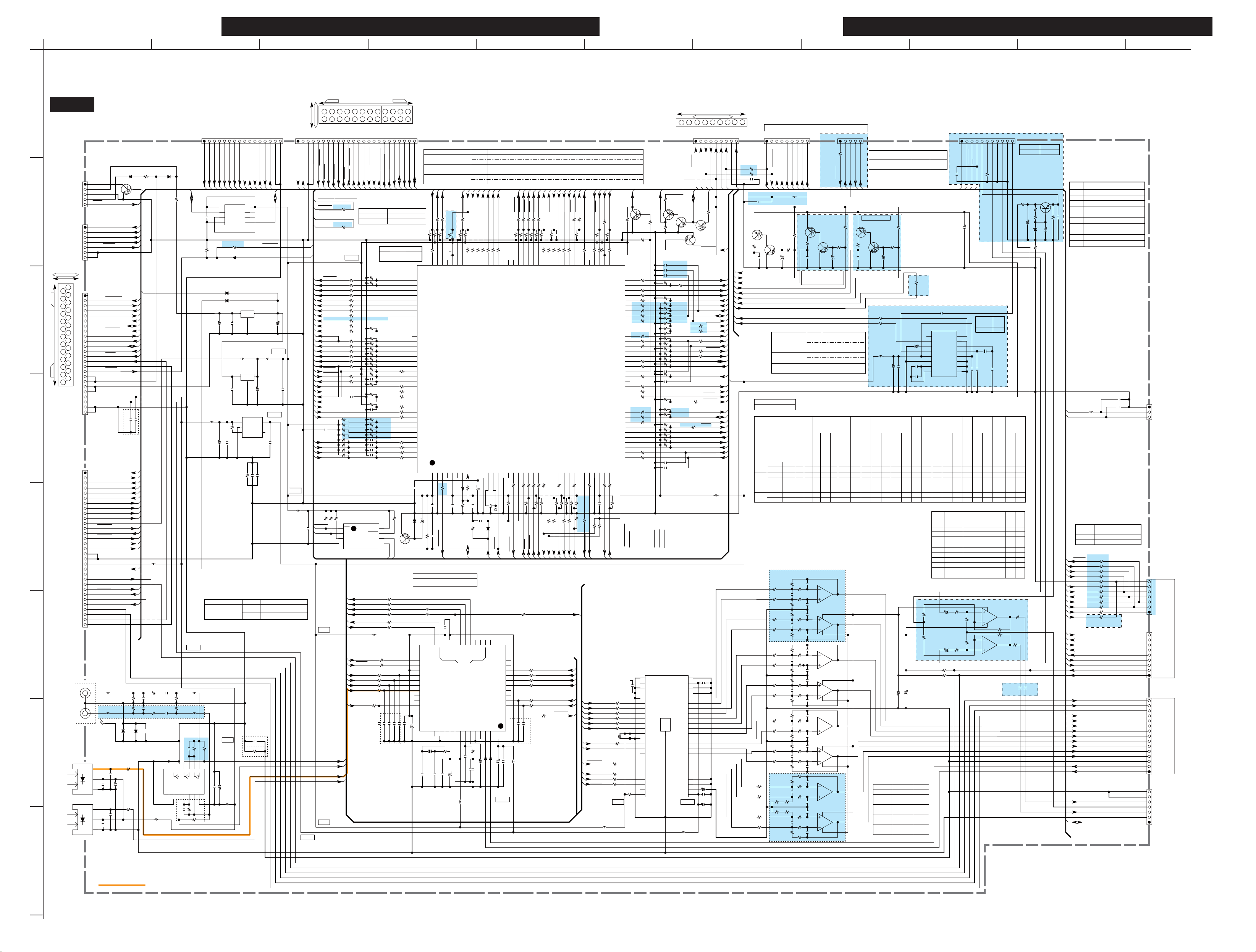
TX-SA578/608 TX-SR308/508/578/608 HT-R280/380/538/580/680/690/C230/C260 DTR-20.2/30.2
TX-SA578/608 TX-SR308/508/578/608 HT-R280/380/538/580/680/690/C230/C260 DTR-20.2/30.2
A
SCHEMATIC DIAGRAMS-6
MPU/ DIR/ DAC Section
1
U0030
MPU, DIR, DAC PC BOARD
BADG-0364
BADG-0364
D183
RL1N4003
MPOWERD
1
+10VS
2
GNDDG
3
JL901B
+12VD_ST
4
POFF
5
TO SD-11a D2 BAETC-0376
TO SD-11b D2 BAETC-0390
1 2
KRC105S
2
SPRLF
1
SPRLCS
2
SPRLSB
3
JL610B
SPRLZ2
4
HPDET
5
GNDDG
6
7
(608 ONLY)
TO SD-8 F3 BATRM-0368
UNDER-TOP
1
2
4
Front
6
8
3
10
12
14
16
18
20
22
Rear
24
26
1
3
5
7
9
11
13
15
17
19
21
23
25
N.C
2
3
P2001A
4
5
6
7
8
9
10
11
12
13
14
15
TO SD-7a K4 BAVD-0375
TO SD-7b K4 BAVD-0389
16
17
18
19
20
21
22
23
24
FANCTRL
UPTDET
UPTTXD
UPTRXD
UPTSCL
UPTSDA
UPTRST
UPTDETINT
VDSWDCTL
VSWSDA
VSWSCL
VMUT
AUX_V
GNDV_AUX
POFF2
+12VD
GNDDG
+5VD_CODEC
+5VA_CODEC
GNDA
SR-608 ONLY
4
(DEL)
LEDPURE
1
REMIN
2
FLDRST
3
P701A
FLDCS
4
FLDCLK
5
FLDSDO
6
KEY0
7
KEY1
8
KEY2
9
KEY3
10
+3.3S
11
KEYINT0
12
LEDSTBY
13
KEYINT1
5
14
VOLA
15
VOLB
16
17
GNDDG
18
+5.0VDIS_
19
LEDZONE2
20
TO SD-10b K3 BADIS-0387
TO SD-10a K3 BADIS-0373
21
22
23
24
25
26
27
28
29
30
31
-15V
MICOUT
+15V
MICDET
MICMUT
AUX_R
LEDTHRU
AUX_L
GNDA_AUX
AUX_V
GNDV_AUX
6
P131
COAX1
COAX2
3
1
4
LBC2518T2R2M
2
LBC2518T2R2M
L131
L132
5
D131
2 1
KDS4148U
7
U131
OPT1
JSR1165-001recieving
U132
OPT2
JSR1165-001recieving
VCC
GND
VCC
GND
1
IN
3
2
1
IN
3
2
104Z
104Z
C141
C142
C143
C144
330J
C145
330J
47
220/10
R142
47
MPOWER
Q181
104Z
C703
C702 104Z
(GNDMIC)
75
R131
75
R132
D132
1 2
R141
UTSP
+12VD
R181
4.7(1/2W)
L746
BLM18PG181SN
R133
10
C131
101J
101J
R134
C132
10
104Z
C130
KDS4148U
LBC2518T470M
KDS4148U
+5.6V_MPU
Q131
L133
+10V
D182
2 1
C133
104K
C134
104K
GND
74HCU04F
OUT49IN4
8
R182
1(1/2W)
CEC
+5.0VA
L135
open
R135
L136
open
R136
C135 080D
OUT511IN512OUT613IN614VCC
10
080D
82K
C136
BCDEF GH
Front
20
22
21
aue9111t24
2021222324
(HDMIINT2)
(HDMIINT_TX)
CEC
DIGSDO
VMUT
DIGSDI
HDMIMUT
POFF2_2
DELETION ITEMS
R706
C521,R615
TX-SR308/HT-R280/HT-R380
HT-R538/HT-RC230 only
(DEL)
R624
10K
R626
10K
R639
10K
R641
10K
R643
10K
R645
10K
R647
10K
R649
10K
R691
10K
R652
R651
10K
1M
R653
C526 102K
R655
R654
10K
R656
R678
10K
R657
(DEL) (DEL)
27K
R659
R658
102K
C524
R660
R661
INT3
R662
Val
INT2
R664
Val
INT1
R666
Val
BAND
R668
Val
102K
R670
C518
102K
C519
R672
102K
C520
R674
102K
C527
R676
R151 10K
8
7
6
5
SI
ROMCLK
ROMSDO
47
R312
47
R313
150
R314
** *
150
R315
47
R316
330
R317
330
330
330
330
330
330
221J
330J
C310 330J
C311
C312
C308 330J
C309 330J
del
del
del
del
24
23
***MPU OPTION RESISOTRS
REF. No.
R539,R540,R541,R542,R633,
R635,R690
R524,R702,R704,R705
VSWSDA
R637
VDSWDCTL
VSWSCL_1
ROMSDI
ROMCLK
ROMSDO
220
47
10K
R619
R623
R621
(NO MIC)
1K
220
220
220
220
220
220
4.7K
4.7K
4.7K
4.7K
KDS4148U
KRC104S
104Z
C307
47
R618
R620
10K
R622
10K
107
106
108
109
110
111
112
113
114
115
116
117
118
119
120
121
122
123
124
125
126
127
128
129
130
131
132
133
134
135
136
137
138
139
140
141
142
143
144
*
C509
D601
1 2
Q601
R502
TX-SA578V/TX-SR608/TX-SA608
HT-RC260/DTR-20.2/DTR-30.2 only
25
26
27
28
29
30
31
32
33
34
35
36
C306
PDL3/AD3
PDL5/AD5/FLMD1
PDL6/AD6
PDL7/AD7
PDL8/AD8
PDL9/AD9
PDL10/AD10
PDL11/AD11
PDL12/AD12
PDL13/AD13
PDL14/AD14
PDL15/AD15
PDH0/A16
PDH1/A17
PDH2/A18
PDH3/A19
PDH4/A20
PDH5/A21
PDH6/A22
PDH7/A23
P715/ANI15
P714/ANI14
P713/ANI13
P712/ANI12
P711/ANI11
P710/ANI10
P79/ANI9
P78/ANI8
P77/ANI7
P76/ANI6
P75/ANI5
P74/ANI4
P73/ANI3
P72/ANI2
P71/ANI1
P70/ANI0
1
2
106K
C2125
104Z
C503
C501
4.7/50
47K
C502 104Z
R501
RESET
(FAN CONTROL)
L301 LM182
L302 LM182
24
MC/SCL
MS/ADR1
MODE
RXIN7/ADR1
RXIN6/ALRCKI0
RXIN5/ABCKI0
RXIN4/ASCKI0
RXIN3
RXIN2
RST
RXIN1
VDDRX
RXIN0
470/10
37
X171
180J
180J
C172
C173
PDL2/AD2
109
AVREF0
1
AVSS
3
R502
FANCTRL
23
GNDRX
38
R331
220
104Z
C313
ADD/DEL
104
BVDD
102K
C521
103
MICMUT
220
R617
R616
10K
102
PCT7
BVSS
ADD
DEL
ADD
DEL
ADD
DEL
VOLB
MICDET
10K
R614
1K
R6131KR611
100
101
PCT5
PCT6/ASTB
R698,R706
NO MIC
100
R615
C522 104Z
105
PDL0/AD0
PDL1/AD1
PDL4/AD4
AVREF1
FLMD0
P11/ANO1
P01/TIP60/TOP60
P00/TIP61/TOP61
7
5
6
104Z
C504
R503
18
19
20
BCK
SCKO
DGND
MDI/SDA
MDO/ADR0
9
8
0
R504
10K
C505
10K
R505
FLMD0
17
LRCK
DOUT
VDD
*
C506
16
MPIO_B3
P10/ANO0
4
220
SR-608 & HIGHER ONLY
104Z
C305
21
22
DVDD
Q301
PCM9210
XTO
FILT
AGND42VCC
41
L304
VCOM45AGNDAD46VCCAD
43
44
472K
C315
C320 223K
C316 473K
LBC2518T4R7M
XTI
39
40
470/10
C314
REMARK(MODEL)
TX-SR308 / TX-SR508 / HT-R280/ HT-R380 / HT-R538/ HT-R580/ HT-RC230
TX-SR578 / TX-SR608 / TX-SA578 / TX-SA608 / HT-R680 / HT-R980 / HT-RC260 / DTR-20.2 / DTR-30.1
TX-SR578 / TX-SR608 / TX-SA578 / TX-SA608 / HT-R680 / HT-R980 / HT-RC260 / DTR-20.2 / DTR-30.1
TX-SR308 / TX-SR508 / HT-R280/ HT-R380 / HT-R538/ HT-R580/ HT-RC230
DTR-20.2 / DT-R30.2
OTHERS
VOLA
LEDTHRU
47
1K
R609
R631
99
PCT4/RD
REGC
VSS
11
10
4.7/50
104Z
C507104Z
D111
14
15
MPO0
MPO1
MPIO_B2
NPCM/INT1
ERROR/INT0
47
680
R332
47/25
C319
LEDPURE
LEDSTBY
LEDZONE2
47
R60647R607
R608 47
95
96
97
PCT298PCT3
PCT1/WR1
X1
12
13X214
X501
1 2
KDS4148U
POFF
RESET
13
MPIO_B1
MPIO_B0
MPIO_C3
MPIO_C2
MPIO_C1
MPIO_C0
MPIO_A3
MPIO_A2
MPIO_A1
MPIO_A0
VINL
VINR
48
470/10
C318
DACRST
47
R716
R715
10K
10K
92
93
91
PCS694PCS7
PCS4
PCS5
PCT0/WR0
Q701
MPD70F3746
P03/INTP0/ADTRG
XT1
XT2
P02/NMI
RESET
15
17
16
18
220
R506
1M
TP01
R508
SYSOUT
R342
12
11
10
R308
9
R307
8
R306
7
R305
6
5
4
R304
3
R333
2
1
NC
C304
del
104Z
L305
LBC2518T4R7M
C317
DIRCS
DACMUT
DACCS
47
220
R60247R603
R605
R708
R709
R604
10K
10K
89
88
PCM490PCM5
40
39
38
37
P05/INTP2/DRST
P04/INTP1
20
19
21
47
220
220
R509
R512
R510
R511
47K
DRST
SYSIN
REMIN2
0
330
330
330
*
330
330
*
R301
330J
C303
del
DSPINT2
DSPRST
DSPINT0
DSPCS
DIRRST
DIVIDE
FHS
47
R599
R601
10K
47
220
R600
10K
R597
R598
85
86
87
PCM0/WAIT
PCM2/HLDAK
PCM3/HLDRQ
PCM1/CLKOUT
DIRINT0
R596
10K
220
R595
84
PCS3/CS3
DSPINT1
C528
104Z
220
220
220
R593
R694
R594
82
81
83
PCS2/CS2
PCS1/CS1
PCS0/CS0
P913/A13/INTP4
74
P915/A15/INTP6/TIP50/TOP50
P914/A14/INTP5/TIP51/TOP51
75
76
CECIO
DSPINPSEL
47
47
R591
R592
47
220
R590
10K
R585
R589
76
79
77
78
PCD280PCD3
PCD0
PCD1
P97/A7/SIB1/TIP20/TOP20
P96/A6/TIP21/TOP21
P95/A5/TIP30/TOP30
P912/A12/SCKB3
P94/A4/TIP31/TOP31
73
P93/A3/TIP40/TOP40
P92/A2/TIP41/TOP41
P91/A1/KR7/RXDA1/SCL02
P90/A0/KR6/TXDA1/SDA02
P80/RXDA3/INTP8
P613/TIP81/TOP81
P612/TIP80/TOP80
P69/TIP70/TOP70
P53/SIB2/KR3/TIQ00/TOQ00/RTP03/DDO
P52/TIQ03/KR2/TOQ03/RTP02/DDI
P51/TIQ02/KR1/TOQ02/RTP01
P50/TIQ01/KR0/TOQ01/RTP00
P55/SCKB2/KR5/RTP05/DMS
P54/SOB2/KR4/RTP04/DCK
P41/SOB0/SCL01
P42/SCKB025P30/TXDA0/SOB4
P06/INTP3
P40/SIB0/SDA01
22
23
24
47
47
R514
R515
R681
R682
47K
10K
VMSDI
VMSDO
VMCLK
47
P34/TIP10/TOP10
P31/RXDA0/INTP7/SIB4
26
R518
10K
R520
R51747R516
RS232TXD
RS232RXD
P3632P37
P35/TIP11/TOP11
P32/ASCKA0/SCKB4/TIP00/TOP00
P33/TIP01/TOP01
27
29
28
31
30
47
47
R688
R686
R519
R523
10K
10K
]
10K
R524
[
)
)
47
47
47
10K
R698
R521
VMRDY
R522
HDMIMUT
R690
(
(
INPSEL
()
ECONRST
10K
VMRST
33
47
R527
R683
10K
DAC_MCK
HDMI_FLR
HDMI_LRCK
33
HDMI_BCK
HDMI_MCK
HDMI_SPDIF
ARC_SPDIF
47
DIRINT0
CX_LRCK
CX_SCLK
DSPSBLR
DSPSLR
DSPCSW
DSPFLR
DAC_MCK
DACRST
DACMUT
DIGSDO
DIGCLK
DACCS
FCLK
REMIN
UPTDETINT
220
R584 10K
R582
220
10K
R581
R583
74
75
73
P911A11/SOB3
P910/A10/SIB3
P99/A9/SCKB1
P98/A8/SOB1
P81/TXDA3
P611/TOP71
P610/TIP71
P68/SCKB5
P67/SOB5
P66/SIB5
P65/RTP15
P64/RTP14
P63/RTP13
P62/RTP12
P61/RTP11
P60/RTP10
P39/RXDA2/SCL00
EVSS
P38/TXDA2/SDA00
EVDD
34
35
36
47
47
R529
R530
104Z
C508
R687
10K
ECONRXD
ECONTXD
22
22
22
22
22
22
C351
470/10
R354
220
R350
R361
R352
R351
+5.0VA
(508-608 UTSJ)
L401
LBC2518T4R7M
1
100
47
47
47
1K
1K
47
47
47
47
47
47
47
47
47
4.7K
4.7K
220
R725
)(
)
)
10K
(DEL)
*
*
*
SYSIN
R577
R538
R723
KRA107S
Q753
10K
R721
SYSOUT
C517 104Z
*
C516 101J
*
C515 101J
*
R576
R693
R572
R570
R568
R566
R563
R562
R707
R559
R557
R554
R552
R551
R586
C514 101J
R588
C513 101J
R543
(
R635
(
R633
10K
R537
R536
R535
R534
C512
C511
KRC102S
Q754
Q756
KRC102S
47
10K
27K
27K
2.2K
2.2K
10K
10K
1K
2.7K
10K
10K
10K
10K
10K
10K
10K
10K
10K
(
R539
22K
22K
22K
22K
102K
102K
(del)*
R544
)
)
10K
R580
47
R579
P615
P614
10K
R531
CECIO
27K
R726
R727
DEL ALL VER.
72
R578
71
70
R575
69
R574
68
R573
67
R571
66
R569
65
R567
64
R565
63
62
61
R560
60
R558
59
R556
58
57
56
R550
55
R548
54
CECOUT
53
R587
52
51
R547
50
R546
49
R545
48
47
R542
46
(
R541
45
(
R540
44
43
42
41
40
39
38
R533
37
R532
Q757
KRC107S
10K
***
*
*
220
220
220
220
220
220
*FOR TX-SR308/508 APPLICATION
23.(HDMISDA)
21. (HDMIINT_TX)
22.(HDMIINT)
27.(HDMIRST)
24.(HDMISCL)
28.(HDMIPDN)
29.(HDMIINT2)
Q302
PCM1690
1
RSV2
2
104Z
C352
R362
4.7K
RSV1
3
RSV2
4
RSV1
5
RSV2
6
LRCK
7
BCK
8
DIN1
9
DIN2
10
DIN3
11
DIN4
12
VDD
13
DGND
14
SCKI
15
RST
16
ZERO1
17
ZERO2
18
AMUTEI
19
AMUTEO
20
MD/SDA/DEMP
21
MC/SCL/FMT
22
MS/ADR0/RSV
23
TEST/ADR1/RSV
24
MODE
C357
104Z
R360
R359
R358
R357
R356
R355
330
330
330
330
+3.3V +5.0VA
RSV2
VCC2
AGND2
RSV2
VOUT1-
VOUT1+
VOUT2-
VOUT2+
THERMALPAD
VOUT3-
VOUT3+
VOUT4-
ePAD
VOUT4+
49
VOUT5-
VOUT5+
VOUT6-
VOUT6+
VOUT7-
VOUT7+
VOUT8-
VOUT8+
RSV2
AGND1
VCOM
VCC1
L402
LBC2518T4R7M
TOP-----------------BOTTOM
23
45
WRITING PORT
P751A
12345
RESET
FLMD0
FLRXD
FSI
RI
+5.6V_MPU
R724
Q755
KRA107S
SYSOUT
FSO
FSI
DIGCLK
DIGSDO
DIGSDI
STEREO
SD
PLLSDA
PLLSCL
47
SR_RST
R564
*
R561
*
SR_RXD
470
SR_TXD
47
UPTTXD
R697
UPTRXD
47
UPTRST
R553
47
UPTSCL
R696
UPTSDA
RDSCLK
RDSDATA
FLDCLK
FLDSDO
FLDCS
220
FLDRST
VSWSCL
VSWSDA
VDSWDCTL
)
47
VMUT
OC_DMS
OC_DCK
OC_DDO
OC_DDI
KEYINT1
KEYINT0
BLM18PG181SN
48
C355
47
46
104Z
45
44
43
42
41
40
39
38
37
36
35
34
33
32
31
30
29
28
C356
27
47/25
26
25
C354
104Z
C353
470/10
7
689
678
FHS
FCLK
FLTXD
+3.3VMPU
FSO
100
+3.3VD
L744
(508/608 UTSJ)
9
0
*
R684
MPOWER_W
0
*
R685
C629 104Z
C630 104Z
Q752
KRA102S
3
2
1K
R712
C613
AMUT
AMUT_C
SBZ2MUT
SBZ2MUT_C
Z2MUT
Z2MUT_C
PRERLSB
PRERLSB_C
RDSCLK
RDSDATA
R560,R561,R564
DD/DC model only
***MPU INITIAL SETTING VALUE***
BAND
INIT1
INIT2
INIT3
SBL-
SBL+
SBR+
SBR-
SL-
SL+
SR+
SR-
SW+
SW-
R410
FL-
15K
R400
FL+
15K
R401
FR+
15K
R411
FR-
15K
TO SD-13 H-8 BAAR-0411
JL601A
12345
RS232TXD
1
KRC104S
2
3
474K
C2125
MODEL
VERSION
C-
C+
678
TRGC
TRGB
Z2VOLCLK
VOLDATA
L600
BLM18PG181SN
R714 10K
R713
2.2K
C751
0.47/50
(SIRIUS)
R669
R668
R667
R666
R665
R664
R663
R662
TRGA
R763
C762
DEL:TX-SR308/HT-R280
HT-R380/HT-RC230
HT-R538/TX-SA608
TX-SR308
DD
PP
PB
DC
MO
DF
MR
MQ
MA
33K
DEL
10K
DEL
DEL
0
DEL
DEL
DEL
DEL
RS232RXD
ECONRST
Q751
1
***MUTE DRIVER SECTION OPTION***
C761,C762,Q761,Q762
R761,R762,R763
C771,C772,Q771,Q772
R771,R772,R773
R784
UP
DOWN
UP
DOWN
UP
DOWN
UP
DOWN
DEL:TX-SR308/HT-R380/HT-R538
R415
15K
R405
15K
R406
15K
R416
15K
R413
15K
R403
15K
R404
15K
R414
15K
R412
15K
R402
15K
R407
15K
R417
15K
R420*R440
R421*R441
22K
R475
R455
1.8K
R465
471J
C405
1.8K
22K
R445
22K
R466
C416
R446
1.8K
R476
471J
C406
1.8K
22K
C426
R456
22K
C423
R473
R453
1.8K
471J
R463
C403
1.8K
R443
22K
22K
C414
R464
R444
1.8K
R474
471J
C404
1.8K
R454
22K
C424
22K
R472
C422
R452
1.8K
R462
471J
C402
1.8K
R442
C412
22K
22K
R467
R447
1.8K
R477
471J
C407
1.8K
22K
R457
C427
*
R430
*
C420
R450
R470
*
*
R460
C400
*
*
C410
C411
R461
*
*
*
R471
C401
*
*
C421
R451
*
R431
9
Z2MUT
DTR-20.2 / DTR-302 ONLY
Q762
KRA102S
3
1
Q761
2
KRC104S
2
1K
3
474K
C2125
ADD/DEL
ADD
TX-SR308/HT-R280/HT-R380
DEL
HT-R538/HT-RC230/TX-SA608
ADD
DEL
ADD
DEL
HT-R280
HT-RC230
DC
33K
10K
10K
10K
DEL
NC
NC
0
0
0
33K
33K
10K
10K
00
DEL
DEL
0
0
00
C425
101J
2
Q404:B
3
NJM4580M-D
101J
C415
NJM4580M-D
4
101J
5
Q404:A
6
8
101J
101J
2
Q403:B
3
NJM4580M-D
C413
101J
NJM4580M-D
4
101J
5
Q403:A
6
8
101J
101J
2
Q402:B
3
NJM4580M-D
101J
NJM4580M-D
4
C417
101J
5
Q402:A
6
8
101J
*
2
Q401:B
3
NJM4580M-D
*
NJM4580M-D
*
4
5
Q401:A
6
8
*
R762
1
VER.REFERENCE No.
OTHERS
OTHERS
TX-SA608
DT-R30.2
OTHERS
HT-R380
MOPPDD
10K
DEL
NC
0
33K
10K
10K
DWL
2.2K
C761
1
7
1
7
1
7
1
7
JL602A
123
0
R704
+10V
REMIN2
R761 10K
0.47/50
HT-R538
PP
10K
DEL
NC
0
33K
10K
10K
10K
5
4
ECONRXD
ECONTXD
+3.3VMPU_232
DEL:TX-SA608
Q772
3
2
1K
R773
474K
C772
C2125
BLM18PG181SN
TX-SR508
DC
PP
PB
MO
MR
MQ
DEL
10K
0
DEL
33K 33K
10K 10K
DEL
DEL
0000
DEL
DEL
REF. No.
R684 R685
R704 L600 C630 JL602A
KRA102S
1
Q771
KRC104S
2
3
R107
R108
DDDCMO
DEL
0
33K
10K
33K
10K
DEL
0
L101
1
100
100
HT-R580
10K
DEL
33K
10K
33K
10K
DEL
0
R772
2.2K
C771
0.47/50
C10410/50
R771 10K
C105104Z
DD PP
DC
DF
DEL
0
DEL
0
DEL
0
DEL
0
TX-SR578
MO
MR
MA
MQ
10K
DEL
DEL
0
DEL
0
DEL
0
-15V
+15V
C498
100/25
***LPF OPTION(FL/FR CHANNEL)***
TX-SA608 MJJ
331J
C400,C401
C410,C411
470J
C420,C421
R420,R421
22K
R430,R431
R440,R441
22K
R450,R451
R460,R461
2.2K
R470,R471
DTR-20.2
DTR-30.2
ADD
R784
C103
10/50
C106
331J
C113
221J
10K
33K
DEL
0
NC
0
DEL
0
C499
100/25
OTHERSREF. No.
471J
101J
10K
12K
1.8K
DEL
0
ONLY
DTR-30.2
1
2
3
4
5
6
7
8
TX-SA578
DC PP DD
33K
10K
DEL
R484
R485
OTHERS
C110 331J
RDSID
RDDA
VREF
MPXIn
Vdda
Vssa
FLout
C In9TEST
HT-R980
DEL
DEL
00NC
33K33K
10K10K
㪁㪁㪁㩷㪤㪬㪫㪠㪥㪞㩷㪪㪜㪫㪫㪠㪥㪞㩷㪭㪘㪣㪬㪜㩷㪁㪁㪁
R802
R806
R807
R808
R810
R811
R813
R822
R823
R824
10K
10K
R499
R498
TO SD-15a G1 BAHDM-0401
TO SD-15b G1 BAHDM-0403
P8001A
1
2345678
[CT/SW]
[BL/BR]
HDMI_MCK
ARC_SPDIF
HDMI_LRCK
HDMI_BCK
HDMI_SPDIF
DSPSBLR
DSPCSW
Q704
1
1OE
VCC
2
1A
2OE
3
1B
104Z
4
C710
GND
SN74CB3Q3305PWR
R702
10K
R110
D110 KDS4148U
1 2
D701 KDS4148U
1 2
D702
KDS4148U
1 2
S812C56AUA
+10S
104Z
C706
C709
470/16
BLM18PG181SN
S812C33AUA
C701
104Z
L742
BLM21PG221SN1
R371
1K
C748100/10
C744104Z
*COAX2 OPTION
ITEMS ADD/DEL VER.
L132,C132,C134,C136,
C308,R132,R134,R136
R138,R140,R323,L136
0
0
+5.0V
82K
10K
R139
R137
1234567
220/10
UTSP
C140 104Z
C139
10K
R138
R140
L134
LBC2518T470M
9
101112
[SL/SR]
DIR_FLR
HDMI_FLR
CX_LRCK
DSPSLR
8
7
6
2B
5
2A
0
Q703
IGO
L747
Q702
IGO
UTSP
C707 100/10
Q746
BH33FB1WG
1
VOUT
VIN
2
GND
3
NC
STBY
GNDA
NC
C800 104Z
R800
ADD OTHERS
DEL
OPTION
C802 104Z
R803
131415
16
DIR_LRCK
GNDA
DIR_BCK
CX_SCLK
CECIO
POFF2_2
POFF2_1
UTSP
C708
470/10
+3.3VS
L743
BLM18PG181SN
106K
C705
+3.3VD
5
4
C745
C2125
106K
C801 103K
+3.3VS
BLM18PG181SN
TX-SR308/HT-R380/HT-R538
NC
TOP-UNDER
P8002A
1234567
[FL/FR]
DIR_MCK
DSPFLR
GNDDG
MPOWER_W
C525 104Z
L153
ROMCS
104Z
C151
ROMSDI
+5.0VA
Rear
246
135
TO SD-15a H2 BAHDM-0401
TO SD-15b H2 BAHDM-0403
(HDMIINT)
DSPINT1
DSPINT2
VMSDI
POFF2_2
REMIN2
(HDMIINT_TX)
VSWSCL_1
VSWSCL
8
7
9
8
1011121314
(HDMISDA)
(HDMISCL)
DSPINT0
DSPCS
VMCLK
VMSDO
(HDMIINT_TX)
0
R706
0
R705
10 121416
9111315 171819
1516171819
(HDMIPDN)
(HDMIRST)
DIGCLK
DSPRST
VMRST
VMRDY
***CONNECTION OPTION
MODEL
TX-SR308/SR508 R702,R704,R705
TX-SR578/SR608
+3.3VS
ROMCS
FLMD1
TRGC
TRGB
TRGA
Z2MUT_C
SBZ2MUT_C
AMUT_C
Z2VOLCLK
VOLDATA
VOLCLK
PRRLF
SPRLF
SPRLCS
SPRLSB
SPRLZ2
PRERLSB_C
MPOWER
HPDET
POFF2_1
SEC1H
IPROTECT
PROTECT
RCPOWER
UPTDET
THERMAL
VOLH
KEY3
KEY2
KEY1
KEY0
10K
R154
+3.3V
0
R627
220
R628
220
R629
220
R630
47
R632
47
R634
47
R636
47
R637
47
R638
47
R640
220
R642
220
R644
220
R646
220
R648
220
R692
220
R650
0
R701
220
R695
C523 102K
R663
Val
R665
Val
R667
Val
R669
Val
2.7K
R671
2.7K
R673
2.7K
R675
2.7K
R677
Q153
2.2K
R1EX25064ASA00A
1
R152 10K
R153
CS
2
SO
3
WP
4
GND
HOLD
DIR_FLR
DIR_LRCK
DIR_BCK
DIR_MCK
DIGSDI
DIGSDO
L303 LBC2518T4R7M
DIGCLK
DIRCS
COAX2
COAX1
OPTI2
OPTI1
47
R625
DIRRST
COAX1
COAX2
OPTI1
OPTI2
+3.3V
DTR ONLY
Vcc
SCK
R321
R322
R323
R324
R325
R326
R327
220
ADD
DEL
Q101
LC72725V
DC
DF
DEL
0
10K 10K
DEL
DEL
DELDELDEL
0
REF_NO
C470
10/50
C471
10/50
IJK
TO TUNER PACK
P101A
3
RDCL
RST
Xout
Vddd
Vssd
MODE
TX-SR308
10
10
C102
16
15
14
13
XIn
12
11
10
TX-SR608
PP
PB
MO
MR
MA
MQ
NC
NC
DEL
HT-R380
HT-R280
HT-R538
DEL
DEL
ADD
DEL
DEL
ADD
ADD
DEL
ADD
ADD
R482
22K
R483
22K
4
2
1
PLLSCL
SD
STEREO
PLLSDA
104Z
C753
470/10
OTHERS
C108150J
C107
104Z
TX-SA608
DD DDPP
MJJMJJ
10K10K10K
33K
33K
10K
10K10K
DEL DEL DEL
HT-RC230
TX-SR508
HT-R580
TX-SR578
R480
27K
27K
R481
JJ/ DC
DD/ DF
3
2
6
5
9
567
8
11
10
VDD_SEL
TU_RI
FM_RDS
GNDTU
GNDTU
+9VTU
TU_LI
0
DEL
R102
DEL
ADD
X101
C109150J
DTR-20.2
TX-SA578
DTR-30.2
DD MA
DEL
DEL
0
0
10K
10K 10K
DEL
DEL DEL
10K
10K
10K
DEL
10K
0
10K
TX-SR608
HT-RC260
DTR-20.2
TX-SA608
R490
1
1K
10K
10K
R491
7
1K
105K
C473
HT-RC260
10K
DEL
10K
10K10K
00000
DELDELDELDEL
000000
HT-R680
HT-R980
TX-SA578
DEL ADD ADD
ADD ADD ADD
DEL DEL DEL
ADD ADD ADD
ADD ADD ADD
DEL DEL DEL
DEL DEL DEL
ADD DEL ADD
DEL DEL DEL
DEL DEL DEL
DEL: TX-SA578/TX-SA608
4
NJM4580M-D
Q405:A
8
R486
R487
Q405:B
NJM4580M-D
DEL: TX-SA578/TX-SA608
OTHERS
22(1W)
R112
C114
10K
DEL
10K10K
10K
10K
10K
DTR-30.2
JJ
47/25
DEL
2SC2235-Y
R113
220
D112
0
R116
ADD
220
R114
MTZJ10VD
NOTE
DEL:Deletion
ADD:Addition
DC Canadian model
DD USA model
DF Taiwanese model
Q111
MO Saidi Arabian model
MQ Hong kong model
33K
PA Australian model
PB U.K. model
R115
C112 104Z
PP
47/25
MP CE(European) country model
C111
MR Chinese model
JJ Japanese model
When don't connect tuner pack, Assemble R116
BLM18PG181SN
+3.3VD
THERMAL
3PIN Socket
5PIN Socket
HPDET
SPRLF
SPRLZ2
SPRLCS
HPGND
PRERLSB
SR_TXD
SR_RXD
SR_RST
SBZ2MUT
Z2MUT
PRRLF
AMUT
VOLH
SEC1H
IPROTECT
PROTECT
VOLCLK
VOLDATA
+15V
-15V
MICOUT
AUX_R
GNDA_AUX
AUX_L
DAC_SBL
DAC_SBR
DAC_SL
DAC_SR
DAC_C
DAC_SW
DAC_FL
DAC_FR
RTAD
LTAD
105K
+15V
-15V
C472
TUNER PACK-GND : SEPARATION
LPF_GND
TU_LO
TUNER_GND
TU_RO
IR_GND
RI
GNDDG
C552
C551 104Z
L500
*P5504A OPTION
TX-SR508/TX-SR578/TX-SA578
TX-SA580/HT-R680/HT-R980
TX-SR508/TX-SR578
OTHERS7PIN Socket
R823
0
R807
0
SPRLB_SPB
R811
0
R813
0
R824
0
R812
0
R810
0
R808
0
R806
0
R822
0
R801
0
R802
0
DTR30.2/608MJJ
VLSC-GND(608MJJ)1117
104Z
1
2
3
JL501B
TO SD-4a J7 BAETC-0343
TO SD-4b H8 BAETC-0350
TO SD-3c B2 BAETC-0357
7
6
5
4
3
2
1
P5504A
9
8
7
6
5
4
3
2
1
P5503A
TO SD-3a F2 BAAF-0341
TO SD-3b F2 BAAF-0348
TO SD-3c F1 BAAF-0355
15
14
13
12
11
10
9
8
7
6
5
4
3
2
1
P5502A
TO SD-3b C2 BAAF-0348
TO SD-3a D2 BAAF-0341
TO SD-3c C1 BAAF-0355
7
6
5
4
3
2
1
P5501A
TO SD-3a B2 BAAF-0341
TO SD-3b B2 BAAF-0348
TO SD-3c B1 BAAF-0355
8
DIGTAL
AUDIO SIGNAL(OPT-1)
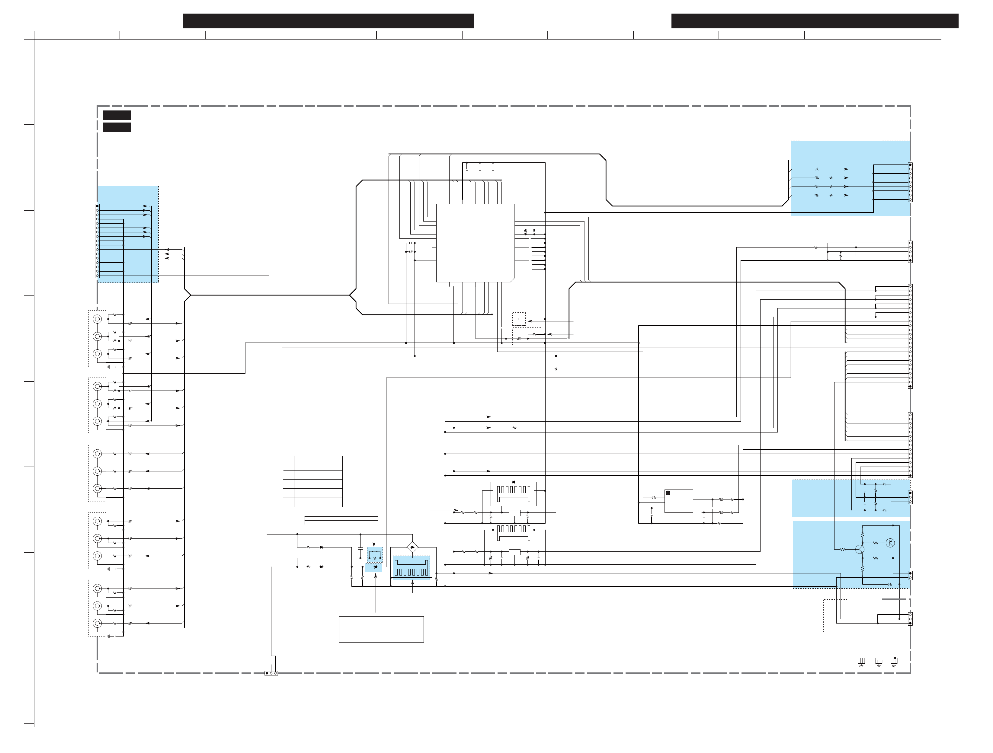
TX-SA578/608 TX-SR308/508/578/608 HT-R280/380/538/580/680/980/C230/C260 DTR-20.2/30.2
TX-SA578/608 TX-SR308/508/578/608 HT-R280/380/538/580/680/980/C230/C260 DTR-20.2/30.2
A
SCHEMATIC DIAGRAMS-7
Video Section
1
U0042 VIDEO PC BOARD BAVD-0375
U0042 VIDEO PC BOARD BAVD-0389 (DTR-20.2/ 30.2 Only)
2
TX-SA578/TX-SA608
ONLY
PR_IN2
1
PB_IN2
2
Y_IN2
3
P2900A
4
5
PR_IN1
6
PB_IN1
7
Y_IN1
8
9
10
PROUT_2
11
To D4 PWB
PBOUT_2
3
PR
(VCR/DVR)
4
COMPONENT
IN2
(DVD)
COMPONENT
IN1
5
COMPONENT
OUT
PB
Y
PR
PB
Y
PR
PB
6
GAME/TV
(VIDEO3 IN)
CBL/SAT
(VIDEO2 IN)
VCR/DVR OUT
(VIDEO1 OUT)
VCR/DVR
(VIDEO1 IN)
7
DVD IN
MONITOR
OUT
12
TO BAVD-0370
13
14
15
16
17
3
P2203
2
1
4
9
7
P2203
6
5
8
12
P2203
11
P2202
P2201
10
13
6
5
4
3
2
1
6
5
4
3
2
1
Y
YOUT_2
DCTRL
GND_VD
+5V
R2116
75
R2115
75
R2157
0
R2114
75
C2203
103K
R2113
75
R2156
0
R2112
75
R2155
0
R2111
75
R2110
75
R2109
75
R2108
75
R2107
75
R2106
75
R2105
75
C2202
102K
7
R2104
75
R2103
75
R2102
75
C2201
102K
7
(D Treminal)
PR_IN2
C2116
1/50
PB_IN2
C2115
1/50
Y_IN2
C2114
1/50
PR_IN1
C2113
1/50
PB_IN1
C2112
1/50
Y_IN1
C2111
1/50
C2110
470/6.3
C2109
470/6.3
C2108
470/6.3
C2107
10/50
C2106
10/50
C2105
470/6.3
C2104
10/50
C2103
10/50
C2102
470/6.3
BCDEF GH
PRIN_2
PBIN_2
YIN_2
PRIN_1
PBIN_1
YIN_1
PROUT_3
PBOUT_3
YOUT_3
VIN_5
VIN_4
VOUT_1
VIN_3
VIN_2
VOUT_MON
DCTRL
SEC2-1
SEC2-2
NOTE
DEL:Deletion
ADD:Addition
DC Canadian model
DD USA model
DF Taiwanese model
MO Saidi Arabian model
MQ Hong kong model
PA Australian model
PB U.K. model
PP
MP CE(European) country model
MR Chinese model
JJ Japanese model
TX-SR308 HT-R280/ 380/ 538/ C230
R9012
1(1/2W)
R9013
1(1/2W)
OTHER
D9014
KDS4148U
D9015
KDS4148U
VOUT_2
POFF2
J2054 TA Jumper
F9001 5A125V
J2054
C9012
334/50
F9001
5A/125V
C9013
4.7/50
R9014
D9016
UDZS6.2B
100K
6 5
DEL:TX-SR308/HT-R380/HT-R538/TX-SR508/HT-R560
HT-RC260/TX-SR608/DTR-20.2/DTR-30.2
TX-SR308(MM,MP)/HT-R380(MM,MP)
TX-SR508(MM,MP)
TX-SA578/TX-SA608
OTHER
YOUT_3
YOUT_1
YOUT_2
PBOUT_1
PBOUT_2
PBOUT_3
C9029
104Z
C9028
470/6.3
According to S2 output
D9011
3
D5SBA20
4
1
2
D9011B
RAD-083
(HDMI No Upcon)
D9016
UDZS7.5B
UDZS6.8B
UDZS5.6B
UDZS6.2B
27
28
29
30
31
32
33
34
35
36
37
38
39
PBOUT3
PBOUT2
PBOUT1
YOUT3
YOUT2
YOUT1
VCC
SCOUT3
SCOUT2
SCOUT1
VCC
SYOUT3
SYOUT2
C9011
PROUT_1
26
PROUT1
SYOUT141GND
40
10000/16
105Z
C2021
C2022
PRIN_1
PRIN_2
PROUT_3
PROUT_2
25
PROUT2
+12V_HD (To HDMI)
+12VMMP
23
24
GND
PROUT3
VOUT2
VOUT3
43
42
VOUT_MON
R9020
8.2(1W)
R9031
3.3(2W)
+12VTRG
20
21
22
PRIN3
PRIN1
PRIN2
Q2001
NJW1326FH2
VIN1
VOUT1
45NC46
44
VOUT_1
(AUX)
(To DSP)+12S
(To U.Port)
R9021
8.2(1W)
R9032
3.3(2W)
(To LAN)
105Z
105Z
C2020
YIN_2
PBIN_2
PBIN_1
15
16
18
17
19
YIN2
YIN3
PBIN1
PBIN3
PBIN2
VIN3
VIN551SYIN152SYIN2
VIN2
VIN4
48
50
47
49
VIN_4
VIN_3
VIN_5
VIN_2
(GAME/TV)
(CBL/SAT)
(VCR/DVR)
(DVD)
2 1
10/50
C9023
2 1
220/25
C9030
YIN_1
14
YIN1
MUTE
SCL
SDA
VCC
GND
SCIN5
SCIN4
SCIN3
SCIN2
SCIN1
SYIN5
SYIN4
SYIN3
105Z
C2011
R9033
1(1/2W)
D9023
KDS4148U
RAD-157
Q9022B
Q9022
NJM78M05
1
I
RAD-140
Q9031B
Q9031
MPC2905BHF
1
I
104Z
C9031
C2025
105Z
C2101
10/50
G
2
G
2
13
12
11
10
9
8
7
6
5
4
3
2
1
C9026
C9027
470/6.3
C2019105Z
C2018105Z
C2017105Z
C2016105Z
C2015105Z
C2014105Z
C2013105Z
C2012105Z
104Z
VMUT
VD_SW_SCL
VD_SW_SDA
H3, D2
ONLY
(AUX_V)
R2101
75
3
O
C9025
470/6.3
3
O
C9033
C9032
470/6.3
AUX_V
R9022
+5V_VD
N.M
EXCEPT
1(1/2W)
H3, D2
(AUX_V)
C2001
10/50
C2002
1
2
3
104Z
Q2002
Vout
VGND
GND
V+
NJM2505AF
C2003
5
4
Vin
C2006
C2004
470J
470/6.3
C2005
470J
470/6.3
R2003
1M
R2001
22
R2002
22
IJK
DEL:TX-SR308/ HT-R380, HT-R538
TX-SR508/ HT-R580
(For HDMI Upcon)
VOUT_2
YOUT_1
PBOUT_1
PROUT_1
C2120
470/6.3
470/6.3
C2119
C2118
470/6.3
C2117
470/6.3
R9043
0.22(1W)
R2119
R2118
R2117
0
0
0
(UPORT LROUT)
DEL:TX-SA578/TX-SA608
ONLY:
(FAN)
TX-SA578V/TX-SR608/TX-SA608
HT-RC260/DTR-30.2/DTR-20.2
R9042
FCTRL
4.7K
R2503
0
GND_DG(GND_VD(MPUGND))
MMPSDA
MMPSCL
MMPRST
MMPRXD
MMPTXD
MMPDET
MMPDETINT
471J
C2031
471J
C2033
22K
R2501
R2502
Q2502
2SC1815
D2, D3
R2505
R2504
330
ONLY
(RS232)
+12VTRG
GND_VD
+5VA_CODEC
+5VD_CODEC
10/50
C2030
220K
R2030
220K
10/50
R2032
C2032
1.2K
2SA950
1.8K
GND_A
ADINPY
ADINPB
ADINPR
+12V_HD
+12V_HD
GNDDSP
AUX_GNDV
VD_SW_SCL
VD_SW_SDA
MMPDETINT
DCKDET1
DCKDET2
Composite
Q2501
C2501
220/25
ADINCV2
GNDP
GNDP
GNDA
GNDA
GND_VD
+12VD
+12VD
POFF2
AUX_V
VMUT
DCTRL
MMPRST
MMPSDA
MMPSCL
MMPRXD
MMPTXD
MMPDET
FCTRL
SDA
SCL
RESET
GND_V
GND_D
Z2_R
Z2_GND
Z2_L
+12V
GND_P
SUBL
GND_SUB
SUBR
1
2
3
P2801A
4
5
6
7
8
9
5
4
3
2
1
24
23
22
21
20
19
18
17
16
15
14
13
12
11
10
9
8
7
6
5
4
3
2
1
15
14
13
RX
12
TX
11
10
9
8
7
6
5
4
3
2
1
1
2
3
1
2
3
2
1
To HDMI PWB
TO SD-16b A-3 BAHDM-0403
JL801A
To HDMI PWB
TO SD-15a J-1 BAHDM-0401
TO SD-18b K-4 BAHDM-0403
To DSP PWB
TO SD-6 A-3 BADG-0364
P2001B
P2002A
TO SD-9 C-3 BAETC-0365
To Universal Port PWB
JL503B
TO SD-3b J-4BAAF-0348
TO SD-3a J-2 BAAF-0341
TO SD-3c B-1 BAAF-0355
To ASP PWB
P2510
From FAN
JL607A
To RS232 PWB
TO SD-20 E-5 BAAR-0411
BAVD-0375
2341
E9002
2341
E9001
NC
321
8
JL952B
TO SD-4a B-8 BAPS-0342
TO SD-3b J-7 BAPS-0349
TO SD-4c B-3 BAPS-0356
To PTRANS FIX PWB
BAVD-0389
2341
E9003
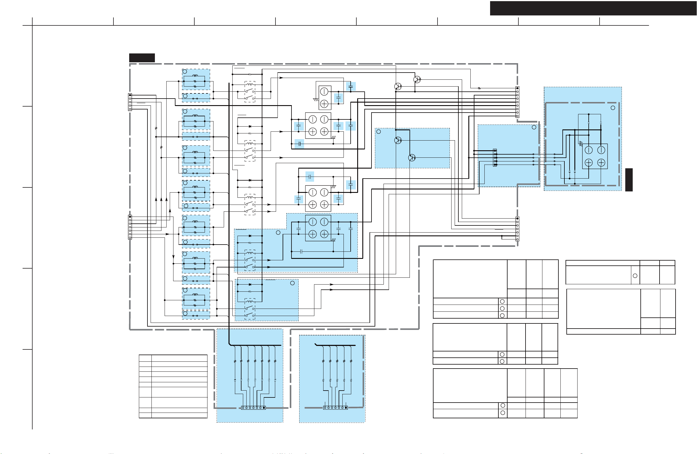
TX-SA578/608 TX-SR508/578/608 HT-R580/680/980/C260 DTR-20.2/30.2
A
SCHEMATIC DIAGRAMS-8
SPEAKER OUTPUT SECTION
1
TO SD-10a B-2 BAETC-0377
TO SD-10b B-7 BAETC-0391
2
3
TO SD-4b F-8 BAAF-0348
TO SD-4c F-8 BAAF-0355
4
5
BCDEFGH
U0060 SP TERMINAL PC BOARD BATRM-0368
BATRM-0368
JL605B
HPL
1
SPLE
2
HPR
3
HPDET
4
5
(TO HP PWB)
GNDDG
R6691
390(1/2W)
R6692
390(1/2W)
JL600B
SPSBL
1
SPSL
2
SPL
3
SPC
4
SPR
5
SPSR
6
SPSBR
7
(MAIN PWB PWB)
NOTE
DEL:Deleton
ADD:Addton
DC Canadian model
DD USA model
DF Taiwanese model
MO Saudi Arabian model
MQ Hong kong model
PA Australian model
PB
MB U.K. model
PP
MP CE(European) country model
MR Chinese model
JJ Japanese model
EXCEPT: 1A/1C
A
L6602 S1.3C
R6602
22
R6612
22
B
J6602
A
L6600 S1.3C
R6600
22
R6610
22
J6600
A
L6601
R6601
22
R6611
22
B
J6601
A
S1.3C
L6603
R6603
22
R6613
22
J6603
B
A
L6604
S1.3C
R6604
22
R6614
22
B
J6604
C
L6605
R6605
22
R6615
22
B
J6605
C
L6606 S1.3C
R6606
22
R6616
22
B
J6606
S1.3C
S1.3C
SPRLCS
1
3
C
L
R
SL
SR
SBL
SBR
4 5
SPRLF
1
3
4 5
SPRLCS
1
3
4 5
SPRLSB
1
3
4 5
1
3
4 5
ONLY:
TX-SR608/ TX-SA608
DTR-30.2/ HT-RC260
SBL
SL
(1W)
(1W)
R6130
8.2
R6135
8.2
R6133
(50V)
(50V)
C6033
C6030
C6035
473J
473J
SBLE
TO SD-4c D-8 BAAF-0355
(MAIN AMP PWB)
C6602
103J
RL6602
D6600
2 1
1SS133
C6600
103J
RL6600
1SS133
2 1
D6603
C6603
103J
RL6603
1SS133
2 1
D6605
C6605
103J
RL6605
1SS133
2 1
D6607
C6607
103J
RL6607
L
(1W)
8.2
(50V)
473J
LE
SLE
R6132
C6032
567
6
2
6
2
6
2
6
2
SPRLZ2
6
EXCEPT: DTR-20.2
2
R
C
(1W)
(1W)
R6134
R6131
8.2
8.2
(50V)
(50V)
C6031
C6034
473J
473J
RE
SBRE
SRE
CE
JL620B
3
4
1
2
D
EXCEPT: DTR-20.2
SR
SBR
(1W)
(1W)
8.2
R6136
8.2
(50V)
(50V)
C6036
473J
473J
C6640
C6650
102J
C6643
C6645
D
P6601
3
C
P6602
2
L
102J
C6655102J
SBL
SL
R
P6603
SR
SBR
HIGHT/WIDE RIGHTHIGHT/WIDE LEFT
103J
103J
103J
1
C6653
2
1
2
1
ONLY:DTR-20.2
SL
(1W)
R6130
R6133
8.2
(50V)
C6033
C6030
473J
TO SD-4c D-8 BAAF-0355
(MAIN AMP PWB)
(1W)
SLE
4
3
4
3
4
3
8.2
2
1
L
(50V)
473J
LE
567
5
5
P6604
5
(1W)
R6132
C6032
CE
4
C6642
C6641
C6644
C6646
C
8.2
(50V)
473J
RE
3
(1W)
R6131
C6031
SRE
2
103J
103J
103J
8.2
(50V)
473J
103J
R
1
C6652
C6651
C6654
C6656
(1W)
R6134
C6034
SR
8.2
(50V)
473J
JL620B
102J
102J
102J
102J
Q6602
RN1205
D
EXCEPT: DTR-20.2
RN1205
Q6603
Q6601
RN1205
SPRLSB
RN1205
Q6604
EXCEPT: DTR-20.2
SPRLZ2
SPRLF
SPRLCS
R6690
10(1/2W)
ONLY:
TX-SR508/TX-SR578/TX-SA508/TX-SA578
HT-R580/ HT-R680/ HT-R980
TX-SR607_(DD/DC/DF)
HT-RC260_(DD/DC)
JL604B
5
Z2RE
4
Z2LE
3
2
Z2R
Z2L
1
TO SD-3b I-3 BAAF-0348
TO SD-3c I-3 BAAF-0355
+22V
GNDRL
SPSBRE
SPSRE
SPRE
SPCE
SPLE
SPSLE
SPSBLE
JL603B
1
2
3
4
5
6
7
8
9
TO SD-4b E-7 BAAF-0348
TO SD-4b E-7 BAAF-0355
(POW AMP PWB)
F
(AUDIO INPUTO PWB)
SPRLF
SPRLCS
SPRLSB
SPRLZ2
HPDET
GNDDG
DEFERENCE NO
L6600-04/ R6600-04/ R6610-14 DEL ADD ADD
LJ604B/ J6600-04 ADD DEL DEL
L6605-06/ R6605-06/ R6115-16 DEL DEL ADD
DEFERENCE NO
JL620B/ C6030-36/ R6103-36 DEL DEL ADD
JL620B/ C6030-34/ R6103-34 DEL ADD DEL
DEFERENCE NO
JL604B ADD ADD DEL DEL
P6607/ J6611-14
C6647/ C6648/ C6657/ C6658
B
1
2
3
JL610A
4
5
6
7
TX-SR508
TX-SR578
TX-SA508
TX-SA578
HTR-580
HTR-680
HTR-980
DC/DD/DF
(DAC/MPU PWB)
TO SD-6 A-2 BADG-0364
DTR-20.2 OTHER
DD ALL
JJ
A
B
C
TX-SR508
TX-SR578
TX-SA508
TX-SA578
HTR-580
HTR-680
HTR-980
DTR-20.2 OTHER
E
H
TX-SR508
TX-SR578
TX-SA508
TX-SA578
HTR-580
HTR-680
HTR-980
ALL
TX-SR608
HT-RC260
DC/DD/DF
F
G
DEL DEL DEL ADD
ONLY:
TX-SR608_(MP/MB//MO/MA/MQ/MR)
TX-SA608/ DTR-30.2/ HT-RC260_PP
BATRM-0369
Zone2 SPK
Banana
102J
102J
C6658
C6657
5
2
J6614
J6613
J6612
J6611
DTR-20.2
DD ALL
P6607
103J
103J
C6647
C6648
RL6605/ C6605/ D6605/ P6604
C6645/ C6646/ C6655/ C6656
RL6607/ C6607/ D6607
OTHER
Z2RZ2L
3 4
1
HIGHT/WIDE RIGHTHIGHT/WIDE LEFT
DEFERENCE NO DT-R20.2 OTHER
Q6603 Q6604
DEFERENCE NO
C6640-44/ C6650-54 ADD DEL
G
U0061
Z2 SP TERMINAL (Banana) PC BOARD
BATRM-0369
DEL ADD
D
TX-SR508
TX-SR578
TX-SR608
DTR-30.2
HT-RC260
HTR-680
HTR-980
PP/PB/MO
MQ/MR/MP
OTHER
ALL
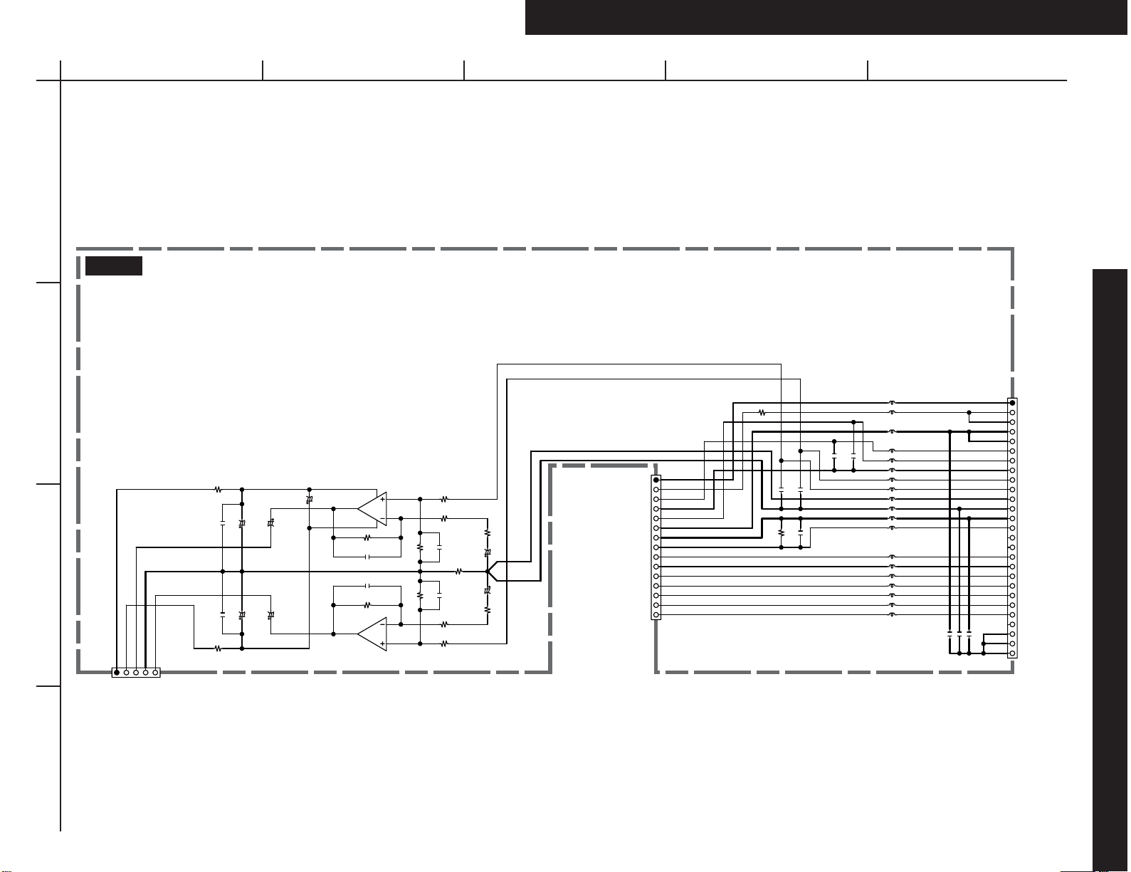
TX-SA578/608 TX-SR308/508/578/608 HT-R380/538/580/680/980/C260 DTR-20.2/30.2
A
SCHEMATIC DIAGRAMS-9
U. Port Unit Section
1
U0031
2
3
TO SD-3a C-2 BAAF-0341
TO SD-3b C-2 BCAF-0348
TO SD-3c C-2 BCAF-0355
TO Audio Input PWB
U. PORT PC BOARD BAETC-0365
R2848
22
C2888
100/25
C2830
104Z
C2889
100/25
R2849
22
104Z
C2829
-15V
1
+15V
U_PORT_R
3
2
JL502B
GND
U_PORT_L
5
4
UTSP
C2877
UTSP
C2878
10/50
10/50
UTSP
UTSP
C2879
BCDE
AUDIO_R
AUDIO_L
1
2
3
4
5
6
7
8
9
10
11
12
13
14
15
16
17
18
19
20
21
22
23
24
25
26
27
P2081
GND_P
+12V
+12V
Z2_L
Z2_R
Z2_GND
TO UP-A1L
TO iPod Dock
10/50
UTSP
NJM4580M-D
7
Q2804:A
R2811
22K
C2880
101J
C2881
101J
R2810
22K
1
Q2804:B
NJM4580M-D
L2800 BLM18PG181SN1D
R2800
FRU090
GND_A
GND_P
1
+12V
2
Z2_L
3
Z2_GND
4
Z2_R
5
GND_D
6
GND_V
7
Composite
8
DCKDET2
9
DCKDET1
10
TX
11
RX
12
RESET
13
SCL
14
SDA
15
P2002B
BAETC-0365
C2851
R2852
R2806
R2807
22K
22K
R2809
22K
R2804
22K
C2882
C2883
R2805
22K
R2808
22K
101J
R2830
101J
AUDIO_R
1M
R2820
C2884
C2885
R2821
470
470
10/50
10/50
UTSPUTSP
MMPDETINT
MMPDET
MMPTXD
MMPRXD
MMPRST
MMPSCL
MMPSDA
TO VIDEO PWB
4
5
6
8
2
3
TOSD-7 K-5 BCVD-0375/BCVD0389
471J
75
C2850
C2852
C2886
471J
470J
L2801 BLM18PG181SN1D
L2802 BLM18PG181SN1D
L2818 BK1608LM182-T
L2817 BK1608LM182-T
471J
471J
C2887
L2816 BK1608LM182-T
L2803 BK1608LM182-T
L2804 BK1608LM182-T
L2805 BK1608LM182-T
L2806 BK1608LM182-T
L2807 BK1608LM182-T
L2808 BK1608LM182-T
L2809 BK1608LM182-T
L2810 BK1608LM182-T
L2811 BK1608LM182-T
L2812 BK1608LM182-T
L2813 BK1608LM182-T
L2814 BK1608LM182-T
L2815 BK1608LM182-T
C2855
104Z
C2854
NC
C2853
NC
TX-SA578/608 TX-SR308/508/578/608 HT-R380/538/580/680/980/C260 DTR-20.2/30.2
4
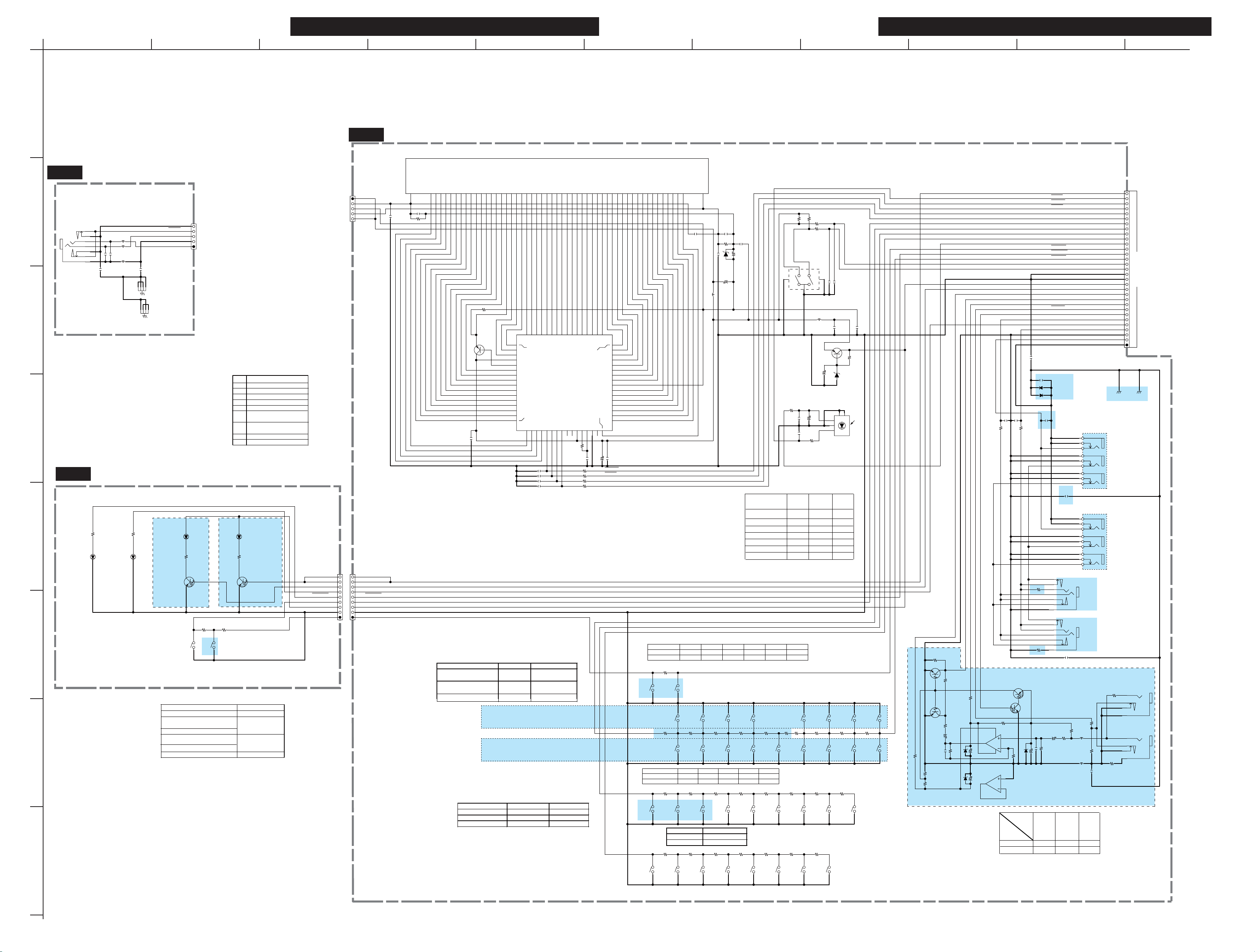
TX-SA578/608 TX-SR308/508/578/608 HT-R280/380/538/580/680/980/C230/C260
S7136
DC,DD,DF,JJ DIMMER
Others RT/TPTY/TP
S7134 S7132
TX-SA578/ 578V CINEMA FILTER LATE NIGHT
TX-SA608 Re-EQ LATE NIGHT
Others MEMORY TUNING
TX-SR508/ 578/ 608
HT-R580/ 680/ 980/ C260
TX-SA578/608 TX-SR308/508/578/608 HT-R280/R380/538/580/680/980/C230/C260
A
SCHEMATIC DIAGRAMS-10a
Display Section
1
U0044 HP PC BOARD BAETC-0377
BAETC-0377
2
GND_DG
HPDET
HPR
SPLE
HPL
EXCEPT T6/A6/HT26
*
T6/A6/HT26 ONLY
E7202
*
*
D7153
GREEN
SLR-342MGTE7P
**
R7153
TX-SR508/TX-SR578/HT-R580/HT-R680
HT-R980/TX-SR608/HT-RC260 ONLY
STBY
TX-SR308/HT-R280/HT-R380/HT-R538
HT-R580/HT-R680/C230
TX-SR508/TX-SR578 (DC,DD)
TX-SR508/TX-SR578/TX-SR608
(EXCEPT:DC,DD)
TX-SA578/TX-SA608
TX-SR608/HT-RC260 (DC,DD)
3
4
5
6
7
8
P7201
5
4
2
3
7
8
MSJ-064-05A_SR
EXCEPT A57/T6/A6/HT26
1
U0041
R7151
RED
D7151
SLI-343URC-TE7
L7201
LBC2518T2R2M
L7202
LBC2518T2R2M
102J
102J
L7203
223K
C7202
*
LBC2518T2R2M
C7203
C7204
*
*
EXCEPT A57/A6
EXCEPT A57/A6
C7201
2341
2341
102J
E7201
KEY SWITCH PC BOARD BADIS-0374
2.2K
STBY
R7152
D7152
YELLOW
SLI-343Y8C-TE7
2.2K
HDMI THROUGH
BCDEF GH
DISPLAY PC BOARD BADIS-0373
Q7002
16-BT-162GNK
P6
P5
P2
16G
15G
14G
18
19
22
24
20
49
50
51
52
53
54
55
56
57
58
59
60
61
62
63
64
26
25
46
48
47
SEG4
SEG3
SEG2
SEG1
SEG0
VCC2
DIG15/SEG39
DIG14/SEG38
DIG13/SEG37
DIG12/SEG36
DIG11
M66005-0001AHP
DIG10
DIG9
DIG8
DIG7
DIG6
DIG5
DIG4
DIG03
DIG02
2
3
1
C7002 104Z
C7003 101J
C7004 101J
C7005 101J
S7106 S7108
SP-A SP-B
ZONE-2 ZONE-2
RIHD
MUSIC OPTIMIZER
27
45
SEG5
DIG01
4
223K
C7017
2G
3G
1G
F11
1
C7011223K
R7007
220
4G
6
8
5
7
TX-SR308
HT-R280/ 380/ 538/ C230
9G
6G
8G
7G
9
11
10
C7001
10G
14
3
2
223K
11G
15
R7001
10K
Q7004
13G
12G
16
17
KTC3875-GR
1
TX-SA578/ 578V/ 608
DEL: TX-SR608/TX-SA608/HT-RC260
ONLY:TX-SR608/TX-SA608/HT-RC260
28
44
SEG6
DIG00
5
P9
P8
29
30
42
SEG7
Q7003
_CS
_RESET
7
6
P10
SEG943SEG8
SCK
P11
31
41
SEG10
SDATA
8
P12
32
40
SEG11
P1
9
N.C.
P13
33P734
39
SEG12
10P011
N.C.
P14
38
SEG13
VCC1
R7002
R7003
R7004
R7005
P15
35
37
SEG14
XOUT
12
R7006
P16
36P437P338
36
SEG15
SEG19
XIN
13
10K
C7007
35
SEG16
VSS
14
N.C.
101J
3.3K
3.3K
220
220
P1823P17
34
SEG17
SEG34
SEG35
15
C7008
39P140
33
SEG18
SEG20
SEG21
SEG22
SEG23
SEG24
SEG25
SEG26
SEG27
SEG28
SEG29
SEG30
SEG31
SEG32
SEG33
16
100/6.3
FLDRST
FLDCS
FLDCLK
FLDSDO
P2021P19
VP
KEY0_1
KEY1
KEY2
KEY3
P21
41
32
31
30
29
28
27
26
25
24
23
22
21
20
19
18
17
104Z
C7009
P22
P24
P25
P23
P26
42
44
47
43
45
46
48
DEL:HT-RC260
ADD:HT-RC260
S7106
ZONE2
TX-SR608/TX-SA608
S7132
TUNING
S7150
TUN UP
P33
P32
P2912P2813P27
P31
P30
50
CODE
515G52
R7103
470
R7106
270
R7115
270
R7123
270
P34
54
53
OFF
S7108
**
S7113
U.PORT
S7114
U.PORT
U.PORT
S7134
MEMORY
*
S7152
49
*
******
CODE
HT-RC260
*
PRESET UP
P35
55
R7107
S7114
DEL
R7116
R7124
C7010
223K
0
TV/CD
330
TV/CD
U.PORT
330
DIMMER
330
ENTER
F22
59
S7115
S7116
*
S7116
TV/CD
U.PORT
S7136
*
S7154
L7032
R7107 R7108 R7109R7106
330
270
R7108
470
R7117
R7125
C7012 223K
R7008
C7016223K
D7002
UDZS8.2B
C7013
33/50
LBC2518T2R2M
S7117
TUNER
S7118
TV/CD
TUNER
S7118 S7120
TUNER
TV/CD
470
S7138
GAME
470
S7156
DOWN
PRESET
470
330
*
C7015
220
C7014
223K
47/16
R7109
560
R7118
560
R7126
560
TUNER
TUNER
AUX
AUX
AUX
MUSIC
TUN DOWN
10K
R7023
10K
R7021
1
4
2
S7002
LBC2518T2R2M
R7041
100
102J
C7042
102J
C7043
TX-SR608 TX-SR308
TX-SA608 HT-R380
R7110 R7130
820
560
R7130
0
PC
AUX
S7122
*
PC
AUX
R7120
S7142
MOVIE/TV
S7160
RETURN
HT-RC260 HT-R538
ADD DEL
DEL ADD
ADD DEL
ADD DEL
ADD DEL DEL
DEL DEL
0270
820
R7111
1.2K
S7124 S7123
GAME GAME
1.2K
S7144
TONE
R7128
1.2K
S7162
SETUP
C7304㩷C7306 C7309
D7301䇭D7302
E7301A
E7301
P7312 R7305
䌐7311 R7304 DEL ADD ADD
䌐7302
䌐7301
560
470
S7119
R7110
820
S7120
*
S7122
R7119
820
S7140
R7127
820
S7158
10K
R7022
10K
R7024
3
5
C7022103K
EC12E2425WITH_WASHER
L7031
Q7033
KTC3875-GR
C7033
C7041
100/6.3
R7042
1K
S7125
CBL/SAT
R7112
2.2K
S7126
CBL/SAT
R7121
2.2K
+
S7146
R7129
2.2K
S7164
DISPLAY
C7021
223K
C7031
312
1
10/16
2
4
3
2
1
U7041
KSM-603TE5B
O䌔HERS
ADD
ADD
DEL
DEL
ADD
R7113
3.9K
R7122
3.9K
103K
R7033
D7033
UDZS3.9B
5
VCR/DVR
VCR/DVR
-
82
S7127
S7128
S7148
C7032
223K
R7114
12K
S7129
BD/DVDBD/DVD
S7130
R7412
DTC114TKA
Q7404
470
220K
100K
NSCT-5P896
5
4
3
2
1
JL605A
FROM SP-OUT PWB
TO SD-8 B-1 BATRM-0368
FROM AMP PWB
TO SD-4a K-4 BAAF-0341
NOTE
DEL:Deletion
ADD:Addition
DC Canadian model
DD USA model
DF Taiwanese model
MO Saidi Arabian model
MQ Hong kong model
PA Australian model
PB
MB U.K. model
PP
MP CE(European) country model
MR Chinese model
JJ Japanese model
*
D7154
S7104
PURE
BLUE
SCB3318E-D2
*
R7154
R7102
330
*
ZONE 2
180
*
Q7153
DTC123JKA
R7101
S7102
CODE
HT-R980
270
PURE AUDIO
120
TX-SR508/TX-SR578
*
Q7154
DTC123JKA
S7104
THX
MUSIC OPTIMIZER
PURE AUDIO
DEL
(EXCEPT:DD/DC)
TX-SA578/TX-SR608
TX-SA608 ONLY
BADIS-0374
U0040
BADIS-0373
1
2
3
4
5
NSCT-5P876
TO -VP PWB
TO SD-3a C-7 BAPS-0342
TO SD-3b C-7 BAPS-0349
9
LEDPURE
8
LEDZONE2
7
LEDTHRU
6
LEDSTBY
5
KEY0
4
+5.0VDIS
3
GNDDG
2
KEY0_1
1
JL953A
TO SD-3c C-7 BAPS-0356
NSCT-9P880
9
8
7
6
5
4
3
2
1
JL702B NSCT-9P880
JL702A
+3.3VMPU
FLAC1
-VP
FLAC2
+3.3VMPU
LEDPURE
LEDZONE2
LEDTHRU
LEDSTBY
KEY0
+5.0VDIS
GNDDG
KEY0_1
R7420
47K
Q7403
DTC114TKA
R7413
R7414
IJK
R7410
R7409
C7405
330J
C7404
220
220
10/16
33K
R7408
D7412
UDZS6.8B
R7411
D7411
UDZS6.8B
470
C7411
C7412
47/16
47/16
C7301
C7302
471J
471J
330
R7301
R7302
Q7005
KRA102S
Q7007
KRC102S
R7406
330
4
5
7
Q7401:A
6
8
NJM4580M-D
NJM4580M-D
1
Q7401:B
1K
R7407
3
2
䌐7401䇭䌒7415 DEL DEL
䌐7402䇭䌒7416
LEDPURE
REMIN
FLDRST
FLDCS
FLDCLK
FLDSDO
KEY0
KEY1
KEY2
KEY3
+3.3S
KEYINT0
LEDSTBY
KEYINT1
VOLA
VOLB
GNDDG
GNDDG
+5.0VDIS
LEDZONE2
-15V
MICOUT
+15V
MICDET
MICMUT
AUX_R
LEDTHRU
AUX_L
GNDA_AUX
AUX_V
GNDV_AUX
104Z
C7305
C7304
*
104Z
D7301
KDS4148U
*
D7302
KDS4148U
*
*
C7309
101J
330
*
C7306
104Z
5
4
R7304
2
*
3
0
7
8
1
5
4
2
3
7
8
R7305
1
*
0
C7303
104Z
P7301
*
1
2
3
4
5
6
7
8
9
NPJ-3PDB693
NPJ-3PDB693
1
2
3
4
5
6
7
8
9
P7302
*
P7311
*
MSJ-035-05ABAGSRLF
P7312
*
MSJ-035-05ABAGSRLF
DEL:TX-SR308/ HT-R280/ HT-R380
HT-R538/ HT-RC230
100
R7401
4.7K
R7404
LBC2518T2R2M
220
LBC2518T2R2M
TX-SR308
HT-R280
HT-R380
HT-R538
HT-RC230
R7403
L7401
L7402
O䌔HERS
ADD
R7402
C7421
220K
102J
C7401
10/16
47K
C7402 101J
R7405
C7403 47/16
D7401
UDZS5.1B
TX-SR608
TX-SA608
HT-RC260
ADD DEL DEL
31
30
29
28
27
26
25
24
23
22
21
20
19
18
17
16
15
14
13
12
11
10
9
8
7
6
5
4
3
2
1
NSCT-31P2161
P701B
E7301A E7302A
**
AUX VIDEO IN
AUX AUDIO L IN
AUX AUDIO R IN
AUX VIDEO IN
AUX AUDIO L IN
AUX AUDIO R IN
AUX PORTABLE IN
AUX PORTABLE IN
SETUP MIC
R7415
2
*
0
5
4
1
P7401
MSJ-035-05CBAGSRtype
*
2
5
4
T6/A6/HT26 ONLY
1
R7416
*
P7402
*
0
MSJ-035-05CBAGSRtype
SETUP MIC
ALL 31P
TO SD-6a A-5 BADG-0364
FROM DIR/DAC/MPU PWB
 Loading...