

Page 1

NSE-8/9 Repairhints
Customer Care Europe & Africa Version 5.0 Approved
Technical Services Training Group Date: 05.09.2001
CONFIDENTIAL 1 (48)
Repairhints
3210
NSE-8/9
© 2001 Nokia Mobile Phones
Checked by:
CC Training Group
Approved by:
Technical Services
Page 2

NSE-8/9 Repairhints
Customer Care Europe & Africa Version 5.0 Approved
Technical Services Training Group Date: 05.09.2001
CONFIDENTIAL 2 (48)
GENERAL
How to use this document
Put the QUICK REPAIR & COMPONENT FINDER layouts behind this manual.
Now you are able to follow these specifications with graphical layouts and it is easier for you to find the
components and measuring points.
Component characteristics:
Some components contain important data.
Several described steps are only practicable if you are able to reflash/realign the phone and/or rewrite
IMEI/SIMlock data in certain cases. Please pay attention to separate notes.
Underfills, broken balls, µBGA
It is not possible to change underfilled components. The trial will damage the PCB surely.
All replaceable µBGA-components must be renewed after removing.
Check soldering points, remove oxidated solderings (broken balls) very careful.
µBGA´s must be soldered only with NMP approved µBGA-rework machines (e.g. Zevac/OK International).
Soldering CSP´s with Hot Air Fan is strictly forbidden!
– refer to General Service Bulletin 106.
Use only recommended fluxtype and always an appropriate amount of it.
PCB handling
Use appropriate cleaning materials only, do not use scratching or rubbing tools. Clean PCB carefully after
every rework and take great pains over the keyboard area. Do not make any loose wiring connections
anywhere.
If it is necessary to change any item located under the metal shields, first remove the shield, do not cut
partially or bend it.
Realign after repair
Characteristics of replacement parts are different.
To prevent additional faults after repair (e.g. low standby time, loosing network etc.) it is necessary
to retune phone values after repair.
© 2001 Nokia Mobile Phones
Checked by:
CC Training Group
Approved by:
Technical Services
Page 3

CONFIDENTIAL 3 (48)
NSE-8/9 Repairhints
Customer Care Europe & Africa Version 5.0 Approved
Technical Services Training Group Date: 05.09.2001
Introduction
IMPORTANT:
This document is intended for use by authorized NOKIA Service Centers only.
The purpose of this document is to provide some further service information for NOKIA 3210 phones.
It contains a lot of collected tips and hints to find failures and repair solutions easily.
It also will give support to inexperienced technicians.
Saving process time and improving the repair quality is the aim of using this document.
We have build it up based on fault symptoms (listed in "Contents") followed by detailed description for further
analysis.
It is to be used additionally to the service manual and other service information like Service Bulletins, for that
reason it does not contain any circuit descriptions or schematics.
All measurements are made with following equipment:
Nokia repair SW : WinTesla Version 6.43
DLL version : NSE8 version 311.02.00 / 13.03.2001
Nokia Module Jig : MJS-13
Digital multimeter : Fluke 73
Oscilloscope : Fluke PM 3380 B
Spectrum Analyzer : Advantest R 3131 with an analogue probe
RF-Generator / : Rohde & Schwarz CMU 200
GSM Tester
While every endeavour has been made to ensure the accuracy of this document, some errors may exist. If any errors
are found by the reader, NOKIA should be notified in writing, using following procedure:
Please state:
Title of the Document + Issue Number/Date of publication.
Page(s) and/or Figure(s) in error.
Please send to: Nokia GmbH
Service & Competence Center Europe
Meesmannstr.103
D-44807 Bochum / Germany
Email: training.sace@nokia.com
Copyright © Nokia Mobile Phones.
This material, including documentation and any related computer programs, is protected by copyright, controlled by Nokia Mobile
Phones. All rights are reserved. Copying, including reproducing, modifying, storing, adapting or translating, any or all of this
material requires the prior written consent of Nokia Mobile Phones. This material also contains confidential information, which
may not be disclosed to others without the prior written consent of Nokia Mobile Phones.
© 2001 Nokia Mobile Phones
Checked by:
CC Training Group
Approved by:
Technical Services
Page 4

CONFIDENTIAL 4 (48)
NSE-8/9 Repairhints
Customer Care Europe & Africa Version 5.0 Approved
Technical Services Training Group Date: 05.09.2001
Contents
PREFACE GENERAL 2
Introduction 3
CHAPTER 1 HW CHANGES IN NSE-8/9 7
-Most importand changes-summary 7
-Charging problems 8
-Not charging 8
-Poor or no service 8
-Time and ringtone problems 8
-Phone does not switch on 9
-L102 soldering problems 9
-Keypad problems 9
-PCN PA Buffer change 9
-N500/501 Philips poweramplifier 10
-Different CCONT N100 versions implemented 10
-New COBBA N200 version implemented 10
-COBBA N200 underfilled 10
-New GSM TX filter 10
HW changes summary for GF boards 12
CHAPTER 2 PHONE DOES NOT SWITCH ON 14
CHAPTER 3 NOT CHARGING FAILURES 22
New PCB (GD7) component & vendor changes 10
-Z700 71MHz filter – New ceramic package 10
HW changes summary for GD7 boards 11
-Does not switch on with battery (also with service battery) 14
-X504 related faults 14
-Power switch S416 faulty 14
-L102 broken soldered 14
-VB line faulty 14
-DC/DC converter V105 faulty 15
-Flash D301 / SRAM D302 related faults 15
-G701 faulty 16
-MAD D300 faulty 17
-CCONT N100 faulty 17
-B100 faulty 17
-Phone does not switch on: SectionDC/DC converter (Flowchart) 19
-Phone does not switch on: Section CCONT (Flowchart) 20
-Phone does not switch on: Flash update not possible (Flowchart) 21
-X101/102 and X503 faulty 22
-F100 faulty 22
-R103 faulty or broken 22
-R125 to R127 connection faulty 22
-C100 broken 22
-Charging problems with ACP – 8/9 charger 22
-Not charging (Flowchart) 23
© 2001 Nokia Mobile Phones
Checked by:
CC Training Group
Approved by:
Technical Services
Page 5

CONFIDENTIAL 5 (48)
NSE-8/9 Repairhints
Customer Care Europe & Africa Version 5.0 Approved
Technical Services Training Group Date: 05.09.2001
CHAPTER 4 LOW STANDBY TIME 25
-Low standby time (Flowchart) 25
-C111, C112, C113, C115 faulty 26
CHAPTER 5 PHONE SWITCHES OFF 27
-Phone switches off (Flowchart) 27
CHAPTER 6 CONTACT SERVICE FAILURES 28
-D301 Flash / D302 SRAM - faulty or poor soldered 28
-D303 EEPROM faulty 28
-COBBA serial fail 28
-CCONT interface fail 28
-Flash update not possible 28
-Contact service: COBBA serial/parallel bus failed (Flowchart) 29
-Contact service: Eeprom tune checksum failed (Flowchart) 30
CHAPTER 7
CHAPTER 8
USER INTERFACE FAULTS 31
Buzzer failed 31
-B400 / board connection broken 31
-Clocktime / Ringtone too fast or too slow - B100 faulty 31
Display faults 32
-Black lines on LCD 32
-No display function 32
-No LCD backlight 32
Keypad faults 32
-Keymat faulty 32
-Board / Dome sheet soiled 32
Internal audio faults 33
-L202/203 faulty 33
-Speaker – no, quiet or distored received audio signal 33
-Microphone – no, quiet or distored transmitted audio signal 33
-X503 – Bottom connector 33
-N200 COBBA faulty 33
-Internal audio failed (Flowchart) 34
SIMCARD FAILURES 35
-“Insert SIMcard” 35
-SIMcard not accepted 35
-X100 Simcard reader 37
-N100, CCONT 37
-V112 faulty 37
-CCONT N100 faulty 37
-“Insert Simcard” failure (Flowchart) 37
© 2001 Nokia Mobile Phones
Checked by:
CC Training Group
Approved by:
Technical Services
Page 6

CONFIDENTIAL 6 (48)
NSE-8/9 Repairhints
Customer Care Europe & Africa Version 5.0 Approved
Technical Services Training Group Date: 05.09.2001
CHAPTER 9 RF PART FAILURES 38
-Low receiver signal strength indicator – antenna faulty 38
-No service or long time to get network coverage 38
-Z501 faulty (low RX quality / GSM 1800 38
-G701 VTCCXO faulty 38
-N600 CRFU faulty / Z600 faulty: “Failed to set high reference…” 38
-No RX in PCN mode only 38
-Z700 faulty – RX calibration fault: “failed to set high reference…” 39
-Z701 faulty – RX calibration fault: “failed to set low reference…” 39
-G700 faulty 39
-N700 faulty 39
-N200 COBBA faulty 41
-No service GSM 900 (Flowchart) 42
-No service GSM 1800 (Flowchart) 43
CHAPTER 10
-Z500 faulty – (low TX power / GSM 900) 44
-Z504 faulty (low TX power / GSM 1800) 44
-N500 / N501 faulty (low TX power GSM 900 / 1800) 44
-TX phase faulty 45
-TX phase faulty in high channel range (GSM 1800) 45
-Faulty spectrum COBBA faulty, CCONT and COBBA broken solderings 46
-TX failure (Flowchart) 47
TX POWER FAULTS 44
Change history 48
© 2001 Nokia Mobile Phones
Checked by:
CC Training Group
Approved by:
Technical Services
Page 7

CONFIDENTIAL 7 (48)
NSE-8/9 Repairhints
Customer Care Europe & Africa Version 5.0 Approved
Technical Services Training Group Date: 05.09.2001
HW changes in NSE–8/9, 3210
MOST IMPORTANT CHANGES - SUMMARY:
Check L102 - version and soldering if phone switches off or does not switch on.
Page# 9 & 14
Clock/Time & ringtone problems - HW changes (SB 17).
Page# 8 & 16
Check R103 version if phone does not charge and check C-Cover version (Time dial removal – SB 24).
Page# 8 & 22
Charging problems with ACP-7 charger if battery is totally discharged (SB 42).
page# 6 & 22
Check if protective label is added / problems to switch on the phone (SB 11).
Page# 9 & 12
Check version of key dome sheet / keypad problems – high keypress force (SB 28 & SB 032).
Page# 7 & 32
Check version of G701 („A“ version must be changed to „B“ version) / poor or no service (SB 018).
Page# 6 & 16
Poweramplifier change and modul version GD7 (SB 030).
Page# 10
New version of 71MHz filter (ceramic package – SB 030).
Page# 10
New CCONT versions (Vs. H to I and to M)– these are not vice versa compatible (SB 030 & SB 040).
Page# 10
New COBBA versions (Vs. 3.1 to 4.1) – these are not vice versa compatible (SB 035).
Page# 10
COBBA underfilled (SB 037).
Page# 10
© 2001 Nokia Mobile Phones
Checked by:
CC Training Group
Approved by:
Technical Services
Page 8

CONFIDENTIAL 8 (48)
NSE-8/9 Repairhints
Customer Care Europe & Africa Version 5.0 Approved
Technical Services Training Group Date: 05.09.2001
CHARGING PROBLEMS
Check if R103 is broken – if resistor was broken or missing: Change N101, too.
Check C-Cover version, cut the arrow of the time dial in cover or change C-Cover if necessary.
(Service Bulletin 024).
NOT CHARGING (with ACP-7 charger only)
If battery is totally discharged – R132 must be changed to 150k / 1% tolerance and R131 must be changed to
82k / 1% tolerance resistor.
For detailed information see Service Bulletin 042.
POOR OR NO SERVICE
13MHz oscillator (G701) must be changed from version “A“ (NGK3092A) to new version “B“ (NGK3092B).
This version “A” VCTCXO is a component used for phones labeled “Made in Finland”, but only within the
IMEI range below mentioned.
First NSE-8 IMEI 448896/10/274359/9
Last NSE-8 IMEI 448896/10/422812/8
First NSE-9 IMEI 448898/10/098643/6
Last NSE-9 IMEI 448898/10/149081/8 (Service Bulletin 018)
TIME & RINGTONE PROBLEMS
In some cases the ringtone and/or the clock work too slow or too fast – in these cases C148 must be changed to 47p, J 50V and
C153 to 18p, J 50V and check 32.768kHz sine- & squarewave signals of B100.
Change oscillator if necessary (Service Bulletin 017).
© 2001 Nokia Mobile Phones
Checked by:
CC Training Group
Approved by:
Technical Services
Page 9

CONFIDENTIAL 9 (48)
NSE-8/9 Repairhints
Customer Care Europe & Africa Version 5.0 Approved
Technical Services Training Group Date: 05.09.2001
PHONE DOES NOT SWITCH ON
Check if track (R132 to L102), located at C110, is printed as upper layer and if this line is 0 Ohm. Also place an isolation label on
this track (see pictures) to protect it for short cuts to D-Cover. This is necessary in IMEI number range below 448896/20/485419/5
and 448896/10/205064/9 (Service Bulletin 011).
L102 SOLDERING PROBLEMS
Check soldering of L102 – In some cases the soldering of the coil can be broken on both sides – change if necessary.
Note the different (approved) versions of L102.
The first (oldest version with soldering problem)
The new versions for better reliability below.
KEYPAD PROBLEMS
High key press force (eg. Navikey,2,5,8,0)
These problems occure due to process change at PCB vendor.
IMEI range: First 448903/10/729000/0
Last 449142/10/432508/8
The PCB´s can be identified by a double arrow symbol on the keypad of the PCB. In this case a new modified keydome sheet is
available to solve this problem.
(Service Bulletin 028 & 032)
PCN PA BUFFER CHANGE
The PCN PA buffer amplifier (N502) is changed from NEC (µpc2771) to RFMD (RF2367) version –
changes apply to HW versions 5.xx. Also the attenuator between the buffer and the PA (R513, R514, R515) is changed from 2dB
to 7dB to compensate the higher saturated power from the RFMD buffer (relative to the NEC buffer
)
© 2001 Nokia Mobile Phones
Checked by:
CC Training Group
Approved by:
Technical Services
Page 10

CONFIDENTIAL 10 (48)
NSE-8/9 Repairhints
Customer Care Europe & Africa Version 5.0 Approved
Technical Services Training Group Date: 05.09.2001
NEW PCB (GD_7), COMPONENT & VENDOR CHANGES
Z700 71MHz FILTER – NEW CERAMIC PACKAGE
If it is necessary to change this filter, please note: The old and the latest type are not compatible and cannot be changed one for
the other!
Old
New
N500 / N501 PHILIPS POWERAMPLIFIER
These are used with GD_7xx PCB only and are not compatible with Hitachi amplifiers (different prints). In case of replacement of
any poweramplifier type, it is necessary to tune the sidebands (CH1 and CH124 for GSM900 and CH512 and CH885 for GSM1800)
in addition to the mid channels (CH60 and CH700) – for tuning instructions see Service Bulletin 020.
DIFFERENT CCONT N100 VERSIONS IMPLEMENTED
1st change is CCONT version 2H to version 2I – This new version can replace the old version, but not vice versa!
nd
2
change is CCONT version 2I to version 2M – New version can replace the old version, but not vice versa!
For detailed information see Service Bulletin 030 & 040
NEW COBBA N200 VERSION IMPLEMENTED
New version COBBA 4.1 can replace the old version COBBA 3.1, but not vice versa!
For detailed information see Service Bulletin 035
COBBA N200 UNDERFILLED
To prevent that symptoms of dropping calls or loosing service appear - resulting from broken solderings under µBGA – underfilling
of COBBA is the solution for those cases. It has been used since IMEI 449143/10/716000/x
NOTE: IT IS NOT POSSIBLE TO REWORK OR REPLACE AN UNDERFILLED µBGA COMPONENT!
For detailed information see Service Bulletin 037
New GSM TX Filter (Z601)
The ceramic version of Z601 is changed to a new version – changes apply to HW versions 5.xx / 55.xx.
These versions can be changed against one for the other.
© 2001 Nokia Mobile Phones
Checked by:
CC Training Group
Approved by:
Technical Services
Page 11

CONFIDENTIAL 11 (48)
NSE-8/9 Repairhints
Customer Care Europe & Africa Version 5.0 Approved
Technical Services Training Group Date: 05.09.2001
OLD NEW
left side: old version / right side: new CSSP version
HW CHANGES SUMMARY FOR GD - BOARD
PCBVers.
GD7_18 54.06 =>
HW
changes.
54.10
Delete Add Remarks
71MHz Filter (4511109)
R717 220Ω (1430734)
R718 220Ω (1430734)
R701 470Ω (1430744)
R606 2.7kΩ (1430832)
C749 1.5pF (2320516)
C617 68pF (2320556)
C618 68pF (2320556)
L600 180nH (3643037)
L601 180nH (3643037)
L701 330nH (3645031)
71MHz Filter (4511161)
R717 330Ω (1430740)
R718 330Ω (1430740)
R701 5.6kΩ (1430772)
R606 5.6kΩ (1430772)
C749 1.8pF (2320518)
C617 82pF (2320558)
C618 82pF (2320558)
L600 220nH (3643079)
L601 220nH (3643079)
L701 390nH (3640077)
GD7_21
GD7_18
to _21
GD7_21 55.45 =>
55.10 =>
55.45
55.60
R315 0Ω (1430690)
C529 1pF (2320629)
D300 MAD V5 (4370489)
C145 100pF (2320560)
C320 10nF (2320620)
C149 1.5pF (2320915)
N100 CCONT 2H (4370393)
71MHz Filter (4511109)
C529 1pF (2320508)
C170 100nF (2320805)
D300 MAD V9 (4370591)
C149 1pF (2320915)
N100 CCONT 2I (4370467)
71MHz Filter (4511161)
New Philips poweramplifier
Atmel Flash IC partially in use
New 71MHz Filter
New CCONT version 2I
New MAD V9 (C07)
MAD V5 HW-ID: 55.82
MAD V5 / GD7_18 HW-ID: 55.16
varistor R103 shifted
GD7_21 55.60 =>
55.61
GD7_21 55.61 =>
R319 680kΩ (1430826)
N200 COBBA 3.1 (4370575) N200 COBBA 4.1 (4370643) New COBBA version 4.1
Change of interrupt level for
CARDDETX in BB
55.75
GD7_21 55.75 =>
Z601 Filt 902MHz (4511015) Z601 Filter 902MHz (4511155) New TX-Filter
55.76
GD7_21 55.76 =>
N100 CCONT2M (4370467) N100 CCONT 2M (4370719) New CCONT version 2M
55.85
GD7_21 55.85 =>
55.91
D300 MAD V9 (4370591) D300 MAD V16 (4370687)
C308 27pF (2320546)
New MAD version 16 ROM 6
GD7_25 New board with selective OSP
© 2001 Nokia Mobile Phones
Checked by:
CC Training Group
Approved by:
Technical Services
Page 12

CONFIDENTIAL 12 (48)
NSE-8/9 Repairhints
Customer Care Europe & Africa Version 5.0 Approved
Technical Services Training Group Date: 05.09.2001
HW CHANGES SUMMARY FOR GF - BOARD
PCB-Version HW-
changes
Delete Add Remarks
GF7_17 3.00 =>
3.02
GF7_17 3.02 =>
3.05
GF7_17 3.05 =>
3.06
GF7_18 4.00 =>
4.05
GF7_18 4.05 =>
4.06
GF7_18 4.06 =>
4.10
GF7_18 4.10 =>
4.
15
GF7_18 =>
GF7_20
4.06 =>
5.00
N114 (4219941)
C153 27pF (2320546)
C232 27pF (2320546)
C233 27pF (2320546)
C242 27pF (2320546)
C243 27pF (2320546)
C148 100pF (2320560)
C153 22pF (2320544)
C232 27pF (2320546)
C233 27pF (2320546)
C242 27pF (2320546)
C243 27pF (2320546)
C148 100pF (2320560)
C153 22pF (2320544)
71MHz Filter (4511109)
R717 220Ω (1430734)
R718 220Ω (1430734)
R701 47Ω (1430744)
R606 2.7kΩ (1430832)
C749 1.5pF (2320516)
C617 68pF (2320556)
C618 68pF (2320556)
L600 180nH (3643037)
L601 180nH (3643037)
L701 330nH (3645031)
D300 MAD V5 (4370489)
C145 100pF (2320560)
C320 10nF (2320620)
C149 2.2pF (2320915)
N100 CCONT 2IH (4370393)
R104 10Ω (1430700)
R619 22Ω (1430710)
R605 1kΩ (1430754)
R727 1.5kΩ (1430758)
R135 330kΩ (1430816)
C307 1nF (2312401)
C613 27pF (2320546)
C205 33nF (2320783)
C122 10µF (2610003)
D300 MAD V5 (4370489)
V114 (4219941)
C153 22pF (2320544)
To get a better TDMA-noise
C148 47pF (2320552)
C153 18pF (2320604)
To get a better TDMA-noise
C148 47pF (2320552)
C153 18pF (2320604)
71 MHz Filter (4511161)
R717 330Ω (1430740)
R718 330Ω (1430740)
R701 5.6kΩ (1430772)
R606 5.6kΩ (1430772)
C749 1.8pF (2320518)
C617 82pF (2320558)
C618 82pF (2320558)
L600 220nH (3643079)
L601 220nH (3643079)
L701 390nH (3640077)
D300 MAD V9 (4370591)
C149 2.2 pF (2320915)
N100 CCONT 2I (4370467)
R619 18Ω (1430708)
R727 1.8kΩ (1430760)
C205 10nF (2320805)
D300 MAD V9 (4370591)
R630 22Ω (1430710)
R320 100Ω (1430726)
R620 270Ω (1430738)
R621 270Ω (1430738)
R335 330kΩ (1430816)
R314 0Ω (1430690)
R327 1kΩ (1430754)
C122 1µF (2312401)
C318 1µF (2312401)
C245 1µF (2320481)
C332 27pF (2320546)
C650 27pF (2320546)
C320 10nF (2320620)
Improvement of amplitude
of 32kHz oscillator
uplink performance
To improve the start up of
32kHz oscillator
uplink performance
To improve the start up of
32kHz oscillator
New CCONT Version 2I
New MAD V9 (C07)
New MAD Version 9 (C07)
© 2001 Nokia Mobile Phones
Checked by:
CC Training Group
Approved by:
Technical Services
Page 13

CONFIDENTIAL 13 (48)
NSE-8/9 Repairhints
Customer Care Europe & Africa Version 5.0 Approved
Technical Services Training Group Date: 05.09.2001
GF7_20 5.00 =>
5.15
GF7_20 5.15 =>
5.16
C145 100pF (2320560)
C320 10nF (2320620)
C149 2.2pF (2320915)
N100 CCONT 2IH (4370393)
R508 47Ω (1430718)
R319 680KΩ (1430826)
C149 2.2pF (2320915)
N100 CCONT 2I (4370467)
R508 68Ω (1430722)
New CCONT version 2I
Improvements in RF/PCN (R508)
Changed interrupt level for
CARDDETX in BB (R319)
GF7_20 5.16 =>
5.30
GF7_20 5.30 =>
5.31
GF7_20 5.31 =>
5.86
GF7_20 5.89 =>
5.90
GF7_20 5.87 =>
5.94
GF7_22 New board with selective OSP
N200 COBBA 3.1 (4370575) N200 COBBA 4.1 (4370643) New COBBA Version 4.1
Z601 Filter 902MHz (4511015) Z601 Filter 902MHz (4511155) New TX-Filter
N100 CCONT 2M (4370467) N100 CCONT 2M (4370719) New CCONT version 2M
L103 60R/100MHz (3203717) L103 470R/100MHz (3203737) L103 changed, which improves
600 KHz modulation spectrum
R514 10Ω (1430700)
R513 470Ω (1430744)
R515 470Ω (1430744)
N502 RF Ampl. (4340263)
R514 47Ω (1430718)
N502 RF Ampl. (4340263)
New PCN PA buffer
RFMD=>
damp adaption: (R513,R514,R515)
© 2001 Nokia Mobile Phones
Checked by:
CC Training Group
Approved by:
Technical Services
Page 14
CONFIDENTIAL 14 (48)
NSE-8/9 Repairhints
Customer Care Europe & Africa Version 5.0 Approved
Technical Services Training Group Date: 05.09.2001
PHONE DOES NOT SWITCH ON
At first always check mechanical appearance of battery connectors X101/X102 if bent or dirty etc. –
defect connectors could cause additional faults like “not charging” or the phone switches off intermittently.
Does not switch on with battery (nor with service battery)
Check if phone works properly in service jig.
Check if BTEMP AD value is in range of 300.
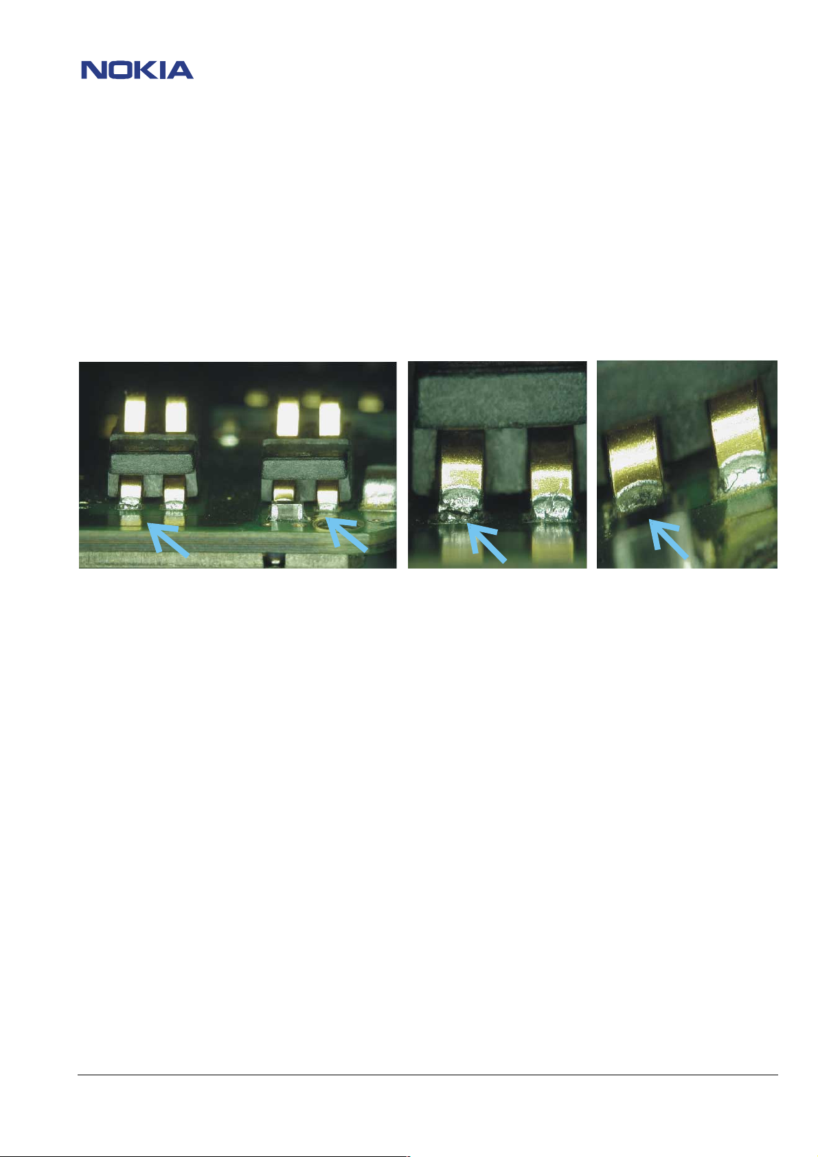
Check battery connectors X101 / X102 for broken solderings or bent spring contacts (see pictures below).
Check if phone works also after connecting LCD module in jig (short circuit in VBB line from LCD possible).
X504 related fault
Check if connector X504 has its correct position – especially after rework in its area.
If it is misplaced or bent, it could cause possible short circuits to D - Cover with throughholes.
POWER switch S416 faulty
Check mechanical condition of S416.
Check if PWRON at R413 drops to 0V during pressing power switch.
Change powerswitch S416 or continue with CCONT chapter on page#17.
L102 broken/poor soldered
Check soldering of L102.
Check resistance of L102 = 0Ω.
Resolder coil or change if necessary.
See the different versions of coil in HW changes chapter on page#9.
VB line faulty
Check battery voltage VB 2.7VDC at L102.
Check VB 2.8VDC at R132.
Check connection (0Ω) between R132/L102.
See HW changes chapter on page#9 for additional PCB protection.
© 2001 Nokia Mobile Phones
Checked by:
CC Training Group
Approved by:
Technical Services
Page 15

CONFIDENTIAL 15 (48)
NSE-8/9 Repairhints
Customer Care Europe & Africa Version 5.0 Approved
Technical Services Training Group Date: 05.09.2001
DC/DC Converter V105 faulty
Check the difference between V101 cathode 3.2VDC / anode 2.6VDC.
Check at V105 – pin 4, 5, 12, and 13: switching frequency 600kHz.
Check 1.2VDC at V105, pin 15.
Check at V105, pin3: 0V. If not, check the respective voltage dividers R131, R132, R134, R143, R144.
If all ok – change V105.
FLASH D301 / SRAM D302 related faults
Check if the current consumption is approximately 20mA.
Try to flash the phone – if this does not work go to chapter “FLASH update not possible” on page#30.
Check also near the service contacts on the PCB - If any component is missing (like on picture below) – flashing will not work!
Torn off components are the result of sliding the phone on the service battery – the contacts can be damaged, too.
NOTE: Always handle the phone in combination with the service battery with care to prevent those failures!
© 2001 Nokia Mobile Phones
Checked by:
CC Training Group
Approved by:
Technical Services
Page 16

CONFIDENTIAL 16 (48)
NSE-8/9 Repairhints
Customer Care Europe & Africa Version 5.0 Approved
Technical Services Training Group Date: 05.09.2001
G701 faulty
Check VCC 2.8VDC at C750 (Phone must be set in local mode).
Check control voltage (AFC) 0.1 – 2.3V at C715.
Check 13MHz reference frequency ±50 Hz (900mVpp) at R743.
NOTE:
If you have to change the oscillator, pay attention to use the correct one
– also see HW changes chapter on page#8
False
Correct
© 2001 Nokia Mobile Phones
Checked by:
CC Training Group
Approved by:
Technical Services
Page 17

CONFIDENTIAL 17 (48)
NSE-8/9 Repairhints
Customer Care Europe & Africa Version 5.0 Approved
Technical Services Training Group Date: 05.09.2001
MAD D300 faulty
Check 32.768 kHz SLEEPCLK squarewave at C145 3Vpp.
Check 13MHz RFC at C301 900 mVpp.
Check VBB 2.8 VDC at C117.
Check SLEEPX 2.8 VDC at J340.
Check PURX 2.8 VDC at R303.
CCONT N100 faulty
Check at R413, if 3.2VDC drops to 0V during pressing powerswitch.
Check SLEEPCLK 32.768kHz squarewave at C145: 3Vpp.
Check VBB 2.8VDC at C117.
Check Vref 1.5VDC at C123.
Check PURX 2.8VDC at R303.
Check VXO 2.8 VDC at C102.
© 2001 Nokia Mobile Phones
Checked by:
CC Training Group
Approved by:
Technical Services
Page 18

CONFIDENTIAL 18 (48)
NSE-8/9 Repairhints
Customer Care Europe & Africa Version 5.0 Approved
Technical Services Training Group Date: 05.09.2001
B100 faulty
Check 32.768kHz sinewave at C153 – 600mVpp.
Check Sleepclock area: C147, C148, C149, C153 and R121-R124.
Check 32.768kHz squarewave at C145 – 3Vpp.
© 2001 Nokia Mobile Phones
Checked by:
CC Training Group
Approved by:
Technical Services
Page 19

CONFIDENTIAL 19 (48)
NSE-8/9 Repairhints
Customer Care Europe & Africa Version 5.0 Approved
Technical Services Training Group Date: 05.09.2001
PHONE DOES NOT SWITCH ON: SECTION DC/DC CONVERTER
Phone does not switch
on, section: DC/DC
converter
Check VB (Battery
2.4V-3V) on L102
OK
Check soldering
and resistance of L102
"0 Ohm"
OK
Check connection
between L102 to R132
(0 Ohm)
OK
Check pin 3 from V105
on="low"status 0V
nOK
nOK
nOK
nOK
Check connector X101/
X102 change if bent or
soiled
Resolder or change L102
Swap the phone if the
connection is open
Check V109 and the
respective voltage deviders
R131,132,134,143,144
OK
Check voltage at
V101 anode 2.6V;
cathode 3.2V
OK
DC/DC converter is ok!
continue with
section CCONT
© 2001 Nokia Mobile Phones
Check 600kHz
nOK
Checked by:
switching frequency at
pin 4,5,12,13 of
V105
Yes
Check 1.2V operation voltage at
Pin 15 of V105
CC Training Group
nOK
nOK
Check soldering of V105 or
change if necessary
Check soldering of V105 or
change if necessary. Also
check R102, R105, R112
Approved by:
Technical Services
Page 20

CONFIDENTIAL 20 (48)
NSE-8/9 Repairhints
Customer Care Europe & Africa Version 5.0 Approved
Technical Services Training Group Date: 05.09.2001
PHONE DOES NOT SWITCH ON: SECTION CCONT
( First disable Watchdog )
Phone does not switch on,
section: CCONT
Check if PWRON (3.2VDC)
drops to 0V during pressing
powerswitch at R413.
OK
Check 32.768 kHz sinewave
(600mVpp) on C153
OK
Check 32.768 kHz
squarewave (3Vpp)l at
C145
OK
Check VXO (2.8VDC) at
C102
OK
nOK
nOK nOK
nOK
nOK
Change S416 if it is
mechanically
damaged
Change B100 if frequency
or amplitude failed
Change N100
Change N100
Check C147/148/153,
R121-124
Check Vbb (2.8VDC) at
C117
OK
Check PURX at R303
(2.8VDC) after pressing
powerswitch
OK
Check 13MHz CLK
frequency
at C301
OK
Try to flash the phone
© 2001 Nokia Mobile Phones
nOK
nOK
nOK
nOK
Checked by:
Change N100
Change N100
Check 13MHz at G701
Continue with section
Flash update not possible
nOK
CC Training Group
Check soldering of G701 or
change if necessary
Approved by:
Technical Services
Page 21

CONFIDENTIAL 21 (48)
NSE-8/9 Repairhints
Customer Care Europe & Africa Version 5.0 Approved
Technical Services Training Group Date: 05.09.2001
PHONE DOES NOT SWITCH ON / FLASH UPDATE NOT POSSIBLE
Does not switch on,
section: FLASH update
not possible
Change Service jig or
Service battery to local mode
if the phone switches off
OK
"MCU boot failure"
appears during flashing
Check 32.768kHz squarewave
at C145 (3Vpp)
OK
Check 13MHz RFCLK
at C301 900mVpp
OK
Check VBB 2.8V DC at C117
OK
Try to flash the phone, if
curre nt consumption is around
20mA
nOK
nOK
nOK
"External RAM error"
appears
during flashing
Continue with section
CCONT
Continue with section
CCONT
Continue with section
CCONT
Swap the phone -
MAD or PCB might be
the reason
© 2001 Nokia Mobile Phones
Yes
nOK
Change FLASH
and try to update again
OK
Phone is OK
Checked by:
nOK
CC Training Group
Yes
Resolder SRAM or
change if necessary
try to update again
OK
Phone is OK
Approved by:
Technical Services
Page 22

CONFIDENTIAL 22 (48)
NSE-8/9 Repairhints
Customer Care Europe & Africa Version 5.0 Approved
Technical Services Training Group Date: 05.09.2001
NOT CHARGING FAILURES
If you are using WinTesla NSE-8/9 with DLL 2.41.03 or lower, the error message “current calibration fail”
will appear in every charge tuning calibration test!
See additional information in Service Manual:
Chapter “Service Software Instructions”, page# 21 (Energy Management Calibration)
X101/102 and X503 faulty
First of all check the mechanical condition of all connectors and clean connector-pads (X503) on PCB and/or change bent or
damaged connectors if necessary –also see pictures on page # 14.
If any connector is poor soldered – additional faults will be the result!
F100 faulty
Check resistance of fuse F100 (0Ω).
Check resistance of V_CHARGE_IN line to GND – should be around 10KΩ.
If the line is in lower-Ohm range, check the PCB for possible liquid or mechanical damages.
R103 faulty or broken
If the phone does not charge when ACP-9 fast charger is connected:
Check mechanical condition of R103 (some versions of this resistor can be broken through mechanical stress)
If the component is broken or is completely missing – change R103 and additional PSCC N101.
(PSCC defect by using charger with broken or missing R103)
If a broken resistor is the reason for this fault, check also C-Cover and cut away the arrow in time dial (by using e.g. scalpel)
or replace it if necessary – see HW changes page# 8 for additional information.
R125 to R127 connection faulty
Check with WinTesla/local mode/Testing/ADC readings if any AD value is out of limits – especially BTEMP (317 ≅≅≅≅ 25°).
Check connection between R125 (near CCONT) and R127 (near X101) = 0Ω and check the resistance of R127 = 47kΩ.
If R127 is broken or poor soldered, the battery indication bar on LCD will appear flashing when charger is connected to phone.
C100 broken
Display-message “Not charging”
Check mechanical condition of C100 (near PSCC) – change capacitor if broken (sometimes only hairline crack)
Check C-Cover (bent or damaged) if C100 is broken – change if necessary
Charging problems with ACP – 8/9 charger
(Sometimes charging stops after LCD light turned off)
Check if the problems do appear with these chargers only and if the phone works properly with ACP – 7 charger.
Check R117 (10kΩ) and R142 (10kΩ) in CHARG_CTRL line if these are poor soldered or in MΩ range – change if necessary.
Check V200 in CHARG_CTRL line for shorts to GND.
Check CHARG_CTRL line to GND.
© 2001 Nokia Mobile Phones
Checked by:
CC Training Group
Approved by:
Technical Services
Page 23

CONFIDENTIAL 23 (48)
NSE-8/9 Repairhints
Customer Care Europe & Africa Version 5.0 Approved
Technical Services Training Group Date: 05.09.2001
NOT CHARGING (1)
Not charging (1)
confirmation or error message/
beep is not coming from phone, if
charger is plugged in
Check V_CHARGE_IN at C100
OK
Check voltage divider R100/101
OK
Change CCONT
nOK
Check system connector
X503, clean contacts & PCB
or change if necessary
OK
Check resistance of fuse (F100)
and L100 (0 Ohm), change if
necessary
© 2001 Nokia Mobile Phones
Checked by:
CC Training Group
Approved by:
Technical Services
Page 24

CONFIDENTIAL 24 (48)
NSE-8/9 Repairhints
Customer Care Europe & Africa Version 5.0 Approved
Technical Services Training Group Date: 05.09.2001
NOT CHARGING (2)
Not charging (2)
error message/beep is
coming from phone if
charger is plugged in
nOK OK
Charge voltage failed
Yes
Try energy
management
calibration
Check BTEMP
A/D in ADC readings
(317=25°C)
Check VCHAR
at voltage divider
R100 / R101
(10:1)=0.8V
nOK
nOK
nOK
OK
Try to charge
after calibration
Check
connection R125
to R127
OK
Check NTC resistor
R127 (47Kohm)
Change N100
(CCONT)
nOK
Swap the phone
if disconnected
© 2001 Nokia Mobile Phones
Battery voltage failed
Checked by:
Yes
Check resistance of
fuse (F100) and
L100 (0 Ohm),
change if necessary
OK
Check R103 if
broken or missing
Check voltage
divider R106/R111
(1:2)
nOK
Check battery
connector X101
X102 change if bent
Yes
Change R103 and
N101 (PSCC)
OK
CC Training Group
Change N100
(CCONT)
Approved by:
Technical Services
Page 25

CONFIDENTIAL 25 (48)
NSE-8/9 Repairhints
Customer Care Europe & Africa Version 5.0 Approved
Technical Services Training Group Date: 05.09.2001
LOW STANDBY TIME
Low standby time
YES
Off state curren t
0-1mA
YES
Sleepmode current
2-8mA
OK
Change N100
Check
charging circuit, try
energy management
calibration
OK
NO nOK
NO
Check resistance
of CCONT output lines
to GND
Check components in
nOK
corresponding lines
Lift L103
OK
Lift C111/112/113
nOK
Lift L505
nOK
OK
Lift L102
OK
Check C109/110,
change V105
Check C107/115,
change N101
Change capacitors
OK
Change N500
nOK
Calibrate RX/TX
values
OK
NOTE: Standby time depends also on
network`s side, signal strength , location
update and users phone handling.
© 2001 Nokia Mobile Phones
Lift L506
nOK
Lift L105 OK
nOK
Change N100
Checked by:
CC Training Group
OK
Change N501
Change N702
nOK
Check consumption of
G700-lift R741
G702-lift R742
nOK
Check capacitors
C718/721/737/739/
754/742, change N700
Approved by:
Technical Services
Page 26

CONFIDENTIAL 26 (48)
NSE-8/9 Repairhints
Customer Care Europe & Africa Version 5.0 Approved
Technical Services Training Group Date: 05.09.2001
C111, C112, C113, C115 faulty
Check the current consumption in different operation modes (refer to the table below).
Check if high current consumption resulting from VB, Vout or output voltages of CCONT.
Disconnect L105 (N702 supply) L505, L506 (PA´s supply) coil by coil and check consumption after every removing.
Check and desolder C111, C112, C113 and C115.
Try Energy Management Calibration if charging stops too early or battery is too hot after charging.
see chapter “NOT CHARGING FAULTS” for additional information.
Current consumption values
Function mode Minimum current in mA Maximum current in mA
Off state 0 1
Sleep mode 2 8
Call mode GSM 900 < 100* < 370**
Call mode GSM 1800 < 100* < 350**
CH60, Power level 19 CH700 Power level 15
Ch60, Power level 5 CH700 Power level 0
Measured with TDS-7
© 2001 Nokia Mobile Phones
Checked by:
CC Training Group
Approved by:
Technical Services
Page 27

CONFIDENTIAL 27 (48)
NSE-8/9 Repairhints
Customer Care Europe & Africa Version 5.0 Approved
Technical Services Training Group Date: 05.09.2001
PHONE SWITCHES OFF
Phone switches off
intermittently
Check if this happens
only with 5V SIM-cards
and if the phone works properly
with 3V SIMcards
nOK
Check 5V
supply voltage at C136
with oscilloscope
nOK
Change C131 if the noise is
higher than 350mVpp
OK
Check X101
and X102,
if poor soldered,
bent or soiled
OK
Check amplitude
of 32.768kHz square
wave at C145, 3Vpp
OK
Check amplitude
of 13MHz RF Clk at
C301 (900mVpp)
OK
Check VBB 2.8V DC
at C117
nOK
nOK
nOK
not OK
Resolder, change or clean
the connectors
Change or check
soldering of B100, C147,
C148, C153, N100
Change or check
soldering
of G701, V702
Change or check
soldering
of N100, C117
C136 10µF/10V
Check if the phone does not switch off with 3V SIM Cards.
Check if VSIM at C136 is approximately 4.8V-5.2V, with maximal 350mVpp noise overlap - see diagram below.
Diagram of normal noise at C136.
© 2001 Nokia Mobile Phones
Checked by:
CC Training Group
Approved by:
Technical Services
Page 28

CONFIDENTIAL 28 (48)
NSE-8/9 Repairhints
Customer Care Europe & Africa Version 5.0 Approved
Technical Services Training Group Date: 05.09.2001
CONTACT SERVICE FAILURES
D303 EEPROM faulty
Check using WinTesla if IMEI or product data are somehow corrupted.
Check 2.8VDC at pin 8 of EEPROM.
Do not use the option "Full factory set" with WinTesla. Otherwise the original IMEI will be changed to "65656565…"
Change EEPROM if it is permitted to you and rewrite all phone data (IMEI, product code…).
If you are not authorized to change EEPROM and the IMEI is missing, write a note with a short comment, and send it together
with the phone to a higher level NOKIA Service Center.
COBBA serial fail
After changing COBBA N200 – take care that all components in the periphery of COBBA are not shifted from their position!
Especially check R765, R766, R233 for the correct position.
CCONT interface failed
Remove Display and check selftest again. If failure persists, change CCONT and check for oxidized pads.
Flash update not possible
D301 FLASH / D302 SRAM - faulty or poor soldered
“Contact service “ appears on LCD
Check with
WinTesla/Testing/Self tests – which of the MCU self test fails
If “MCU ROM Checksum failed” appears or if the phone does not switch on:
Check current consumption. If continuously around 20mA, try to flash the phone.
If the fault remains after flashing:
Check soldering of SRAM D302
Change Flash D301 and try to flash the phone again.
If “MCU RAM Interface failed” or
if “MCU RAM Component failed” appears:
Check 32.768KHz Sleepclock squarewave at C145 (3Vpp).
Check 13MHz RFC at C301 (900mVpp).
Check VBB at C117 – 2.8VDC.
Resolder SRAM D302 and try to flash the phone.
If any error message appears during flashing (“External RAM error”), change SRAM D302 and retry.
If error message persists, change Flash D301 and flash again.
If the failure persists, probably MAD D300 or PCB faulty.
© 2001 Nokia Mobile Phones
Checked by:
CC Training Group
Approved by:
Technical Services
Page 29

CONFIDENTIAL 29 (48)
NSE-8/9 Repairhints
Customer Care Europe & Africa Version 5.0 Approved
Technical Services Training Group Date: 05.09.2001
CONTACT SERVICE - COBBA PARALLEL / SERIAL BUS FAILED
COBBA parallel/
serial bus failed
Check COBBACLK 13MHz
3.6Vpp at J201
OK
Check VBB 2.8V at C117
OK
Check VCOBBA 2.8V DC at C248
nOK
nOK
nOK
Check 13MHz RFC
at C301 900mVpp
OK
Swap the phone, as
MAD or PCB might
be the reason
Check soldering or
change N100, C117
Change or check
soldering of N100,
C248
nOK
Check soldering or
change G701, V702
Check COBBA reset impulse
during initialization routine
Change the COBBA
© 2001 Nokia Mobile Phones
OK
at J343
OK
not OK
Checked by:
Swap the phone, as
MAD or PCB might
be the reason
CC Training Group
Approved by:
Technical Services
Page 30

CONFIDENTIAL 30 (48)
NSE-8/9 Repairhints
Customer Care Europe & Africa Version 5.0 Approved
Technical Services Training Group Date: 05.09.2001
CONTACT SERVICE – EEPROM TUNE CHECKSUM FAILED
EEPROM tune
checksum failed
Check with WinTesla
all product information,
if any phone data like IMEI, product
code, PSN, etc. is anyhow
corrupted
Yes
Reset the phone
No
do not use full factory
set if it is not pe rmitted to you
to rewrite the IMEI
Check 2.8V DC at
EEPROM pin 8
EEPROM
internal fault
OK
nOK
OK
Phone is ok if CONTACT SERVICE
dissapears
nOK
Check VBB at C117
© 2001 Nokia Mobile Phones
Change EEPROM if it is
permitted to you, to rewrite
the IMEI
For detailed
information see
General Service Bulletin 026
Checked by:
CC Training Group
Send these phones to a
higher level
NOKIA Service Center
if it is not permitted to you to
rewrite the IMEI
Approved by:
Technical Services
Page 31

CONFIDENTIAL 31 (48)
NSE-8/9 Repairhints
Customer Care Europe & Africa Version 5.0 Approved
Technical Services Training Group Date: 05.09.2001
USER INTERFACE FAULTS
BUZZER FAILURE
Buzzer failure
Check
buzzer control signal
from MAD 2.8Vpp at
N400 pin 3
OK
Check VDC_OUT
3.9V DC at N 400 pin 1 and
"+" at B400
OK
buzzer signal 5Vpp at N400
Check
pin 6 and "-" of B400
OK
Change B400
nOK
nOK
nOK
Swap the phone because
MAD or PCB might be
the reason
Check connection to
VDC_OUT at V105,
pin 1/16
Check VBB 2.8V DC at
pin 2 of N400
OK
Change N400
nOK
Check VBB 2.8V DC
at C117
B400 / board connections broken
Check buzzer control signal from MAD at N400, pin 3: 2.8Vpp / 1kHz
(use WinTesla/Testing/Audio Level 1, 1000Hz)
Check VDC_OUT 3.9VDC at N400, pin 1 and at Plus-pin of buzzer.
Check VBB 2.8VDC at N400, pin 2.
Check buzzer signal at Minus-pin of buzzer: 5Vpp, 1kHz.
Check board connection N400, pin 6 to Minus-pin of buzzer.
Change buzzer if all ok.
Clock time / Ringtone too fast or too slow - B100 faulty
Check Sleepclock 32.768kHz squarewave at C145 – 3Vpp
Check B100, C147, C148, C153, N100.
See Service Bulletin 017 for additional information (value change: capacitors C148, C153).
© 2001 Nokia Mobile Phones
Checked by:
CC Training Group
Approved by:
Technical Services
Page 32

CONFIDENTIAL 32 (48)
NSE-8/9 Repairhints
Customer Care Europe & Africa Version 5.0 Approved
Technical Services Training Group Date: 05.09.2001
Display Faults
If one or more lines are missing completely as in picture below, change LCD unit
Faulty display sample
Black lines on LCD
Check VBB 2.8VDC at C400 and R421
If voltage ok, change LCD
No display function
If backlight works, but no symbol on LCD appears, in the most cases there are broken solderings under CCONT N100
No LCD backlight
Check VDC_OUT = 3.2VDC at V406, V409, V412, V413
Use WinTesla/Testing/User Interface/1.Test Pattern “on”/”off”.
Check LCD_LED line at N400, pin 9: 1.2VDC in “on” mode / 1.9VDC in “off” mode.
Check cathode of V406, V409, V412, V413: 1.2VDC “on”/ 1.9VDC “off”.
Check LCD_LIGHT line at N400, pin 7: 2.8VDC “on”.
Check also soldering of R415 and/or for shorts to GND.
KEYPAD FAILURE
Keymat faulty
Check the bottom of keymat for broken pins or mechanical damage.
Board / Dome Sheet soiled
If there are only one or two keys without function, check and clean the keyboard area and Dome Sheet if soiled.
NOTE: Different versions of Dome Sheets are available If all faulty keys are in the same ROW or COL line, check connections between the corresponding keys and to GND.
If any line is disconnected between the keys, swap the unit as PCB is faulty.
see HW changes on page# 9.
© 2001 Nokia Mobile Phones
Checked by:
CC Training Group
Approved by:
Technical Services
Page 33

CONFIDENTIAL 33 (48)
NSE-8/9 Repairhints
Customer Care Europe & Africa Version 5.0 Approved
Technical Services Training Group Date: 05.09.2001
INTERNAL AUDIO FAULTS
L202, L203 faulty
Check resistance from L202, L203 to speaker pads normal 0Ω.
Check resistance from L202, L203 to GND and between both lines, Normal: high resistance range >1MΩ.
Speaker - No, quiet or distorted received audio signal.
Check mechanical condition of speaker.
Check resistance of speaker - around 30Ω.
Microphone – No, quiet or distorted transmitted audio signal.
Check contact pads of microphone.
Check resistance of microphone - around 800Ω.
Check microphone voltage 1.7VDC at C242 (use WinTesla/ Testing/ Audio/ internal/ Loop on).
Check audio signal at C258 and C259.
X503 – Bottom connector
Check microphone contact springs in connector.
Check contact springs to the board. Change connector if bent.
Clean the contact pads on PCB.
N200 COBBA faulty
Check VBB 2.8VDC at C117 near CCONT.
Check VCOBBA 2.8VDC C248 near COBBA.
Check COBBACLK 3.6Vpp at J201 - see diagram at page# 41.
Check COBBARESET impulse during initialization routine at J343 (see diagram "COBBA RESET").
Change COBBA (if not underfilled) and rewrite IMEI and SIMlock data.
If error persists - MAD or PCB might be the reason.
SWAP the unit because MAD is not changeable.
Note:
Rewrite SIMlock and IMEI entries with Nokia Security Password and make a SW-update or send these
phones to a higher level NOKIA Service Center!
© 2001 Nokia Mobile Phones
Checked by:
CC Training Group
Approved by:
Technical Services
Page 34

CONFIDENTIAL 34 (48)
NSE-8/9 Repairhints
Customer Care Europe & Africa Version 5.0 Approved
Technical Services Training Group Date: 05.09.2001
INTERNAL AUDIO FAILURE
Internal audio failure
Speaker does not work
(received audio)
Microphone
does not work
Check
Yes
connection L202, L203
to speaker pads
(0 Ohm)
OK
nOK
Check the mechanical
appearence and
impedance of speaker
nOK
(around 30 Ohm)
Check contact springs
Yes nOK
and impedanc e of microphone
(800 Ohm)
Ok
Check microphone bias
voltage 1.7V at C242
(audio loop enable)
nOK
Change L202 or L203
Change speaker
Change microphone
Check voltage at R214
nOK
nOK
nOK
Check resistance
between lines and
GND: >1MOhm
Change COBBA
(N200)
Check if the
connection X503 to
PCB is soiled
Change N200
COBBA
Change
N200 COBBA
© 2001 Nokia Mobile Phones
Ok
Check audio signal
at C258, C259
Ok
Check 2.8V DC VBB at C117
and 2.8V DC VCOBBA at C248
Ok
Check
COBBACLK 13MHz 3.6Vpp at
OK nOK
J201and COBBARESET at J343
during initialization
Checked by:
nOK
nOK
Follow signal back to
the microphone
continue with CCONT
chapter on page #17
Swap the phone because
MAD or PCB might
be the reason
CC Training Group
Approved by:
Technical Services
Page 35

CONFIDENTIAL 35 (48)
NSE-8/9 Repairhints
Customer Care Europe & Africa Version 5.0 Approved
Technical Services Training Group Date: 05.09.2001
SIMCARD FAILURES
First of all – always check the mechanical condition of all connectors: X100, X101, X102 and
change if contact springs are bent, soiled or possible torn off traces/pads under X100.
Also check solderings of connectors and areas for possible liquid damages.
“INSERT SIMCARD”
Check if the phone works properly with a Test SIM.
If Test SIM works check R115, R116 (both 100
Check at SIMcard reader if VSIM is pulsed to 3/5Vpp, refer to VSIM picture – if not, change N100 if necessary.
Check SIM lines and especially V112 for shorts to GND.
Check components in SIM lines (R115, R116 and C137 – C141) for short circuits or capacity loss.
Ω) if these are in a high Ohm range.
“SIMCARD NOT ACCEPTED”
Open with WinTesla/View/Quick-RF-info, to see if a possible SIMlock is activated.
Compare the data listed in MCC & MNC with SIMlock list for the respective product code.
If SIMlock settings are ok, but the MSIN data field is closed to any special IMSI data range:
ONLY the provider is allowed to open this SIMlock!
If the listed data does not fit to the product code:
Correct SIMlock settings with NOKIA Security Password, if this procedure is permitted to you.
If SIMlock is not active and/or SIMcard is still not accepted after correct data input – change COBBA N200
NOTE:
After rework of COBBA it is necessary to rewrite SIMlock data with NOKIA Security Password if it is permitted to you.
© 2001 Nokia Mobile Phones
Checked by:
CC Training Group
Approved by:
Technical Services
Page 36

CONFIDENTIAL 36 (48)
NSE-8/9 Repairhints
Customer Care Europe & Africa Version 5.0 Approved
Technical Services Training Group Date: 05.09.2001
If other SIMcard problems appear, check the following signals at SIMcard reader pins:
SIMclock (pin x), SIMdata (pin 4) – but note:
These signals are only present when SIMcard is active (e.g. when phone registers to the network).
SIMreset (SIMRST_0) is low active, which means that SIMcard will be reseted when SIMreset is 0V.
This is the case after switching on the phone (see next diagram).
While VSIM is already high, SIMreset keeps low for a few milliseconds – in this time SIMcard will be reset.
© 2001 Nokia Mobile Phones
Checked by:
CC Training Group
Approved by:
Technical Services
Page 37

CONFIDENTIAL 37 (48)
NSE-8/9 Repairhints
Customer Care Europe & Africa Version 5.0 Approved
Technical Services Training Group Date: 05.09.2001
X100, SIMcard reader
Check soldering
Check contacts - change connector if bent
N100, CCONT
Check SIMDATA (Pin 4 SIMreader), SIMClock 3.25MHz (Pin 3 SIMreader), SIMReset (Pin 2 SIMreader) and
VSIM 3V/5VDC (Pin 1/5 SIMreader) depends on used SIMcard
See diagramss on page# 36.
V112 faulty
Change component if SIMDATA, SIMClock, SIMReset or VSIM is short circuited to GND
Check R115, R116, C137, C138, C139, C140, C141 for short circuits or capacity loss
CCONT N100 faulty
Refer to “Insert SIM Card” procedure – see Flowchart on page# 37.
COBBA N200 faulty
Change COBBA if all SIM LOCK entries and SIMcard signals from CCONT are ok
Swap the phone if component is underfilled!
Note:
Rewrite SIMlock and IMEI entries with Nokia Security Password and make a SW-update or send these phones
to an authorized NOKIA Service Center.
“Insert Simcard” failure
Insert SIMcard
the phone does not
register the SIMcard
Check soldering and
contacts of X100,
SIM-reader
OK
Check SIM-data,-clock,-reset and
VSIM for shorts to GND
OK
Change N 100 CCONT
nOK
nOK
Resolder X100 or change if any
contact spring is bent
Change V112 if SIM -DATA,
-CLOCK, -RESET or VSIM is short
circuited to ground
OK
Check R115,R116,
C137,C138,C139,
C140, C141
nOK
Swap the phone whether
any contact pad of
SIM-reader is torn off
© 2001 Nokia Mobile Phones
Checked by:
CC Training Group
Approved by:
Technical Services
Page 38

CONFIDENTIAL 38 (48)
NSE-8/9 Repairhints
Customer Care Europe & Africa Version 5.0 Approved
Technical Services Training Group Date: 05.09.2001
RF PART FAILURES
In case of any fault you suppose in the RF part of your phone: Try to calibrate RX/TX-values first to define the fault.
Refer to spectrum samples on page#46
Low receiver signal strength indicator – Antenna faulty
Check the fixed position of the antenna – do not touch the conductive area with bare fingers!
Check spring connector X501 – change if spring contacts are bent (the GND spring will always look bend down a bit)
Check the indicator level with a new antenna.
No service or long time to get network coverage
Check sleepclock frequency 32.768kHz at B100 – change B100 if frequency does not fit
(see also chapter “Phone does not switch on – B100 faulty”)
Z501 faulty (low RX Quality / GSM1800)
If RX calibration fails – see RF part faults in previous chapter
If RX calibration works or in some cases the low reference level cannot be set – check if Z501 bent
Change Z501 if necessary
No service failures summary
At first set the RF-Generator to a high RF-level output: e.g. –40dBm
Use WinTesla to set the phone in the following mode: Local mode/Testing/RF Controls/Active unit “RX”/continuous mode
G701 – VCTCXO faulty
Check 13MHz reference frequency at SUMMA N700, pin 15 – frequency error ±50Hz / 900mVpp
(see also chapter “Phone does not switch on – G701 faulty”)
If all voltages ok and no frequency deviation is realized, but intermittent call interrupts occuring over and over again - it is also
possible that G701 has a not detectable internal failure – so change G701 if the phone has those intermittent call problems.
N600 CRFU faulty / Z600 faulty: “failed to set high reference …”
Check the incoming RF-frequency (e.g. GSM/CH60: 947MHz) at N600, pin 27
Check LNA_AGC (FRACTRL) at N600, pin 28: 2.8VDC
Check VRX_1 at N600,
Check LNA_OUT 2.3VDC at N600, pin 23 and output of Z600 (attenuation in/out ~15dBm) at N600, pin 18, 19
(In some cases it could be possible that Z600 shorts LNA_OUT)
Check UHF LO frequency (GSM/CH60 = 2036MHz) at N600, pin 4 (app. –20dBm) –
Check 71MHz intermediate frequency output at N600, pin 15, 16.
Check soldering of N600 and/or change CRFU if necessary.
pin 33, 38, 45, 46: 2.8VDC
No RX in PCN-mode only
Check IF 187MHz at N600 pin 45, 46 (out) and pin 11, 12 (in)
Check IF 71MHz at N600 pin 15, 16 (out)
Check ¼ VHF 116MHz at N600 pin 9
Check V_VHF = 2.8V at N600 pin 13 – if not ok, change CCONT N100
for additional information see Service Bulletin 018
Frequency deviation 0Hz!
© 2001 Nokia Mobile Phones
Checked by:
CC Training Group
Approved by:
Technical Services
Page 39

CONFIDENTIAL 39 (48)
NSE-8/9 Repairhints
Customer Care Europe & Africa Version 5.0 Approved
Technical Services Training Group Date: 05.09.2001
Z700 faulty – RX calibration fault: “failed to set high reference …”
Check 71MHz intermediate frequency at Z700 in and out (attenuation ~15dBm)
Check components in output lines of Z700 (C701, C704, C749, L701, R701) if output amplitude is different between both lines.
Check for possibly broken solderings under the component.
Z701 faulty – RX calibration fault: “failed to set low reference …”
Check 13MHz intermediate frequency output at N700, pin 30
Check 13MHz IF input at N700, pin 25, 26 (attenuation in/out ~20dBm)
Check 13MHz IF at Z701 (attenuation in/out ~5dbm)
Check soldering of Z701 or change if necessary
Check IF input lines (N700, pin 25, 26) to GND - 10k
Ω - and periphery of Z701 (R717, R718, R719, C706)
G700 faulty
Check UHF frequency at G700 for high spurios emission and/or frequency deviation
Check VDC_OUT at N702, pin 6 and also VDC_OUT connection to L103
Check connection from N702, pin 4 to R741
Check VCP 5VDC supply voltage at N700, pin 13, 22
If VCP lower than 4.8VDC check components in VCP line back to CCONT and/or change N100 if necessary
Check UHF VC at N700, pin 21: 1.9V – 3.2VDC depending on the used channel
Check VC with oscilloscope for noise – check especially soldering of R733
Check C136 (e.g. for capacity loss) if UHF frequency is not adjustable only in higher channel range
Change G700 if necessary
N700 faulty
Check 13MHz reference frequency at N700, pin 15: 900mVpp (frequency deviation ±50Hz)
Check VRX_2 at N700, pin 35: 2.8VDC
Check incoming 71MHz IF at N700, pin 37, 38 and outgoing 13MHz IF (measurable level approximately -20dBm) at N700, pin 30
If 13MHz IF does not exist or a frequency error appears – check VHF_LO at N700, pin 8
Check VCC of G700 and G702 (check connection between both oscillator VCC´s to N702, pin 4) and R745
Check VP1/VP2 at N700, pin 9, 19: 2.8VDC
Check VCP 5VDC at N700, pin 13, 22
Check PLL control signals at N700, pin 5 (SCLK), pin 6 (SDAT), pin 7 (SENA) – see following diagrams
Check VC of G700 at N700, pin 21 (PD2) depending on the used channel and VC of G702 at N700, pin 12 (PD1): 2.2VDC
Check soldering of N700 or change SUMMA if necessary
© 2001 Nokia Mobile Phones
Checked by:
CC Training Group
Approved by:
Technical Services
Page 40

CONFIDENTIAL 40 (48)
NSE-8/9 Repairhints
Customer Care Europe & Africa Version 5.0 Approved
Technical Services Training Group Date: 05.09.2001
© 2001 Nokia Mobile Phones
Checked by:
CC Training Group
Approved by:
Technical Services
Page 41

CONFIDENTIAL 41 (48)
NSE-8/9 Repairhints
Customer Care Europe & Africa Version 5.0 Approved
Technical Services Training Group Date: 05.09.2001
N200 COBBA faulty
Check 13MHz IF at N700, pin 23, 24 – if the generator level (-80dBm….-105dBm) is changing - amplitude of IF must also change
Check RXC signal at N700, pin 36 – if the generator level is changed – the amplitude of signal must also change
Check R725 if these signals are not measurable or too low in amplitude –
Check VBB 2.8VDC at C117 (near CCONT)
Check VCOBBA 2.8VDC at C248 (near COBBA)
Check COBBACLK at J201: 3.6Vpp –
see diagram below
If all signals and voltages are ok – set the phone in call mode with CMU/CMD
Check the RX/TX values while knocking (with a nonmetallic item) around COBBA
If any error appears – probably broken solderings under COBBA - change N200 if possible (if not underfilled)
If the errors persist after rework of COBBA – MAD or PCB might be the reason
NOTE: If COBBA or MAD is underfilled – swap the phone, because these components are not changeable!
If COBBA was changed - SIMlock and IMEI entries must be rewritten with NOKIA Security Password, if this
procedure is permitted to you!
see diagram below
© 2001 Nokia Mobile Phones
Checked by:
CC Training Group
Approved by:
Technical Services
Page 42

CONFIDENTIAL 42 (48)
NSE-8/9 Repairhints
Customer Care Europe & Africa Version 5.0 Approved
Technical Services Training Group Date: 05.09.2001
NO SERVICE GSM900 - First check TX spectrum if it is only a receiver fault, see spectrum samples on page# 46.
Failed to set low
reference
Change Z700
Change Z701
nOK
nOK
Failed to set high
reference
Check 71MHz IF
at C617/C618
OK
Check IF 71MHz at
N700 pin 37/38
OK
Check IF 13MHz
in/out at Z701
nOK
Check 13MHz
Ref.frequency at
N700, pin 15
OK
Check
GSM LNA
947MHz at N600,
pin 27
OK
Check 947 MHz
in/out at Z600
nOK
nOK
nOK
Change G701
Check Z500/503
Change Z600
OK
Check IF
Change N700
nOK
13MHz at N700
pin 23/24
OK
Change COBBA
(N200)
NOTE : If COBBA or D301 has been changed,
SIMLOCK & IMEI data have to be rewritten.
Also realign RX/TX values.
OK
OK
Check UHF2036
MHz at N600 pin 4
OK
Check UHF
2036MHz at G700
nOK
Check Vc&Vcc
at G700
nOK
nOK
Change N600
Change G700
© 2001 Nokia Mobile Phones
Checked by:
CC Training Group
Approved by:
Technical Services
Page 43

CONFIDENTIAL 43 (48)
NSE-8/9 Repairhints
Customer Care Europe & Africa Version 5.0 Approved
Technical Services Training Group Date: 05.09.2001
NO SERVICE GSM1800 - First check TX spectrum if it is only a receiver fault, see spectrum samples on page# 46.
Failed to set low
reference
Check Z501 if bent
OK
Check PCN_LNA at
N600, pin 34
OK
Check 1842.8MHz
in/out at Z602
OK
Check 13MHz RFCLK
900mVpp
OK
Check UHF 2029.8MHz
at G700 & N600, pin 4
OK
Check 187MHz at
N600, pin 45/46
OK
Check 1/4 VHF 116MHz
at N600, pin 9
nOK
nOK
nOK
nOK
nOK
nOK
nOK
OK
Change Z501
Check PCN_LNA at
Z504, Z503, X501, X500
Change Z602
Change G701
Change G700
Change N600
Check 71MHz IF at
C617/C618
OK
Check 71MHz IF at
N700, pin 37/38
OK
nOK
nOK
Change N700
Change Z700
© 2001 Nokia Mobile Phones
Check values at N700
and G702
NOTE : If COBBA or D301 has been
changed, SIMLOCK & IMEI data
have to be rewritten.
Also realign RX/TX values.
Checked by:
Check 13MHz IF at
Z701, in/out
OK
Check 13MHz IF at
N700, pin 23/24
OK
Change COBBA
CC Training Group
nOK
nOK
Change Z701
Change N700
Approved by:
Technical Services
Page 44

CONFIDENTIAL 44 (48)
NSE-8/9 Repairhints
Customer Care Europe & Africa Version 5.0 Approved
Technical Services Training Group Date: 05.09.2001
TX Power faults
FOR DETAILED TROUBLESHOOTING AND FURTHER INFORMATION SEE SERVICE MANUAL CHAPTER 4/GSM & 5/PCN TRANSMITTER
Z500 faulty – (low TX power / GSM900)
Check TX power level difference at Z500 between TX pad & Antenna pad
Check soldering of Z500
Z504 faulty (low TX power / GSM1800)
Check switching voltage at Z504 (C507): 1VDC
Check TX power difference at Z504 between TX pad & Antenna pad
If the difference > 2dBm – change Z504
N500 / N501 faulty (low TX power GSM900 / GSM1800)
All hints are always for both bands (GSM/PCN) – so take only the band depending on your faulty one
Check VDC_OUT 3.2V …. 4.2V (depending on power level) at N500 / N501
Check input / output power difference at N500 / N501
Check CTL_GSM signal at N500 (1.2Vpp …. 1.9Vpp – depending on the used power level) at N700, pin 31
Check CTL_PCN signal at N501(1.0Vpp …. 1.6Vpp – depending on the used power level) at N700, pin 28
(see diagram below)
Change corresponding PA if control lines are ok
CTL_PCN signal at N700, pin 28 – in this example measured at power level 0
© 2001 Nokia Mobile Phones
Checked by:
CC Training Group
Approved by:
Technical Services
Page 45

CONFIDENTIAL 45 (48)
NSE-8/9 Repairhints
Customer Care Europe & Africa Version 5.0 Approved
Technical Services Training Group Date: 05.09.2001
TX phase faulty
Check TX spectrum with analyzer – refer to page# 46
If the following spectrum appears – check components in TX I/Q lines for shorts:
In some cases (especially after rework in COBBA area) R708, R710, C708, C709 (near COBBA N200) could be misplaced.
If the components are ok – change COBBA N200 if not underfilled.
NOTE:
If COBBA was changed - SIMlock and IMEI entries must be rewritten with NOKIA Security Password, if this procedure is
permitted to you!
TX phase faulty in high channel range in GSM1800
Check TX spectrum with analyzer – refer to page# 46
Check mechanical appearance of Z504
If measurements are ok – change Z504 – in some cases the bottom side of this component could be teared off because of
mechanical stress, which only could be seen if the component is removed.
© 2001 Nokia Mobile Phones
Checked by:
CC Training Group
Approved by:
Technical Services
Page 46

CONFIDENTIAL 46 (48)
NSE-8/9 Repairhints
Customer Care Europe & Africa Version 5.0 Approved
Technical Services Training Group Date: 05.09.2001
Faulty spectrum – COBBA faulty, COBBA and CCONT broken solderings
1)
Normal spectrum 3) Spectrum of faulty COBBA
2)
Spectrum with broken solderings under CCONT 4) Spectrum of faulty oscillator G500
Turns to picture 1 if CCONT is pushed
careful with some nonmetallic item
© 2001 Nokia Mobile Phones
Checked by:
CC Training Group
Approved by:
Technical Services
Page 47

CONFIDENTIAL 47 (48)
NSE-8/9 Repairhints
Customer Care Europe & Africa Version 5.0 Approved
Technical Services Training Group Date: 05.09.2001
TX FAILURE
GSM900 faulty GSM1800 faulty
OK
Check 116MHz
at N700, pin 44/45
OK
Check 116MHz
at N600, pin 25/26
OK
Check UHF 2036MHz
at N600, pin 4
OK
nOK nOK
nOK
Check 13MHz RFCLK 900mVpp
at N700, pin15.
Change if faulty.
OK
Check VHF 464MHz
at N700, pin 8
Change N700
Check Z702
Check/change G700
OK
nOK
nOK
nOK
Change G702
Check 232MHz at
N700, pin 46
Check 232MHz at
N600, pin 35/37
Check UHF 1979.8MHz
at N600, pin 4
OK
OK
OK
Check
PA_GSM 902MHz at
N600, pin 22
OK
Check
PA_GSM 902MHz
at N500, pin1
OK
Check PA_GSM at
N500, pin 4
OK
Check PA_GSM at L500,
Z503/Z500, X500/X501
Change Z504
nOK
nOK
nOK
Change N600
Check Z601 (in/out)
Check Z603,N502,Z502
Check at N500/501, pin 2:
CTL_GSM=0.7-1.7Vpp
CTL_PCN=0.12-0.2Vpp
( squarew ave, de pends on Pow er-level )
OK
Check VC at Z504
0.9Vpp squarewave
nOK
nOK
nOK
nOK
OK
Check PA_PCN
1747.8MHz at N600,
pin 40
OK
Check PA_PCN
at N501, pin 1
OK
Check PA_PCN
at N501, pin 4
OK
Check PA_PCN
at Z504 (Ant. conn.)
nOK
Check/change L503
OKI
Check/change:
a) N600 / b) N100
if not ok, MAD faulty
© 2001 Nokia Mobile Phones
Check at N503:
nOK
Checked by:
a) pin 2 BAND_SEL (lowlevel)
b) pin 1 VTX 2.8V pulsed
CC Training Group
Check PA_PCN
at Z503, X500/501
Approved by:
Technical Services
Page 48

CONFIDENTIAL 48 (48)
NSE-8/9 Repairhints
Customer Care Europe & Africa Version 5.0 Approved
Technical Services Training Group Date: 05.09.2001
Change history
Originator Status Version Date Comment
Jose
Marquez
Jose
Marquez
Jose
Marquez
Holger
Klein
TS-TrainingGroup
TS-TrainingGroup
TS-TrainingGroup
Draft 0.2 22.10.1999 First draft version for the repair group
Draft 0.3 02.11.1999 Insert comments from the repair team, add layout
"Test Points"
approved 1.0 05.11.1999 First AMS version
approved
approved
2.0
3.0
04.02.2000
07.09.2000
“not charging” reference to SB024 added
Additions to chapter “no service”
SIM-Locks updated
Flowcharts page 15, 21 VCOBBA at C148 corrected
to C248
New appearance, RF- descriptions, Flowcharts and
HW changes added. All documents reworked.
approved 4.0 20.10.2000 Headers changed.
approved 4.2 31.10.2000 Last SIMlock-list and Comments added.
TS-TrainingGroup
TS-TrainingGroup
draft 4.6 27.08.2001 Comments from repair team added, SIMlock list
removed (separated)
approved 5.0 05.09.2001
© 2001 Nokia Mobile Phones
Checked by:
CC Training Group
Approved by:
Technical Services
 Loading...