

Page 1

PAMS Technical Documentation
NSE–8/9 Series T ransceivers
Troubleshooting
Issue 1 07/99
Page 2

NSE–8/9
PAMS
Troubleshooting
Technical Documentation
CONTENTS
Abbreviations in fault finding charts 3. . . . . . . . . . . . . . . . . . . . . . . . . . . . . . . . .
Baseband Trouble Shooting 4. . . . . . . . . . . . . . . . . . . . . . . . . . . . . . . . . . . . .
4.1. Phone is totally dead 5. . . . . . . . . . . . . . . . . . . . . . . . . . . . . . . . . . . .
4.2. Flash programming doesn’t work 6. . . . . . . . . . . . . . . . . . . . . . . . .
4.3. Power doesn’t stay on or phone is jammed 11. . . . . . . . . . . . . . . .
4.4. Display Information: Contact Service 13. . . . . . . . . . . . . . . . . . . . . .
4.5. The phone doesn’t register or phone doesn’t make a call 13. . . .
4.6. Plug in SIM card is out of order . 17. . . . . . . . . . . . . . . . . . . . . . . . . .
4.7.Audio fault. 20. . . . . . . . . . . . . . . . . . . . . . . . . . . . . . . . . . . . . . . . . . . . .
4.8. Charging Fault 23. . . . . . . . . . . . . . . . . . . . . . . . . . . . . . . . . . . . . . . . .
RF Troubleshooting 25. . . . . . . . . . . . . . . . . . . . . . . . . . . . . . . . . . . . . . . . . . . . .
PCB Bottom view(GF7) 26. . . . . . . . . . . . . . . . . . . . . . . . . . . . . . . . . . . . . . . . . . .
PCB Top view (GF7 + GD7) 26. . . . . . . . . . . . . . . . . . . . . . . . . . . . . . . . . . . . . . .
2. GSM Receiver 27. . . . . . . . . . . . . . . . . . . . . . . . . . . . . . . . . . . . . . . . . . . . . . . . .
2.1 .General instructions for GSM RX troubleshooting 27. . . . . . . . . . . . . . . .
2.2 .Path of the received GSM signal 27. . . . . . . . . . . . . . . . . . . . . . . . . . . . . . .
2.3.Fault finding chart for GSM receiver 28. . . . . . . . . . . . . . . . . . . . . . . . . . . . .
3. PCN Receiver 31. . . . . . . . . . . . . . . . . . . . . . . . . . . . . . . . . . . . . . . . . . . . . . . . .
3.1 .General instructions for PCN RX troubleshooting 31. . . . . . . . . . . . . . . . .
3.2 Path of the received PCN signal 31. . . . . . . . . . . . . . . . . . . . . . . . . . . . . . . .
3.3 Fault finding chart for PCN receiver 32. . . . . . . . . . . . . . . . . . . . . . . . . . . . .
4. GSM Transmitter 36. . . . . . . . . . . . . . . . . . . . . . . . . . . . . . . . . . . . . . . . . . . . . .
4.1 General instructions for GSM TX troubleshooting 36. . . . . . . . . . . . . . . . .
4.2 Path of the transmitted GSM signal 36. . . . . . . . . . . . . . . . . . . . . . . . . . . . . .
4.3 Fault finding chart for GSM transmitter 37. . . . . . . . . . . . . . . . . . . . . . . . . . .
5. PCN Transmitter 38. . . . . . . . . . . . . . . . . . . . . . . . . . . . . . . . . . . . . . . . . . . . . .
5.1 General instructions for PCN TX troubleshooting 40. . . . . . . . . . . . . . . . . .
5.2 Path of the transmitted PCN signal 40. . . . . . . . . . . . . . . . . . . . . . . . . . . . . .
5.3. Fault finding chart for PCN transmitter 41. . . . . . . . . . . . . . . . . . . . . . . . . .
6. Synthesizers 44. . . . . . . . . . . . . . . . . . . . . . . . . . . . . . . . . . . . . . . . . . . . . . . . . .
6.1 General instructions for Synthesizer troubleshooting 44. . . . . . . . . . . . . . .
6.2 13 MHz reference oscillator 44. . . . . . . . . . . . . . . . . . . . . . . . . . . . . . . . . . . .
6.3.VHF VCO 44. . . . . . . . . . . . . . . . . . . . . . . . . . . . . . . . . . . . . . . . . . . . . . . . . . . .
6.4.UHF VCO 45. . . . . . . . . . . . . . . . . . . . . . . . . . . . . . . . . . . . . . . . . . . . . . . . . . . .
6.5.Fault finding chart –UHF VCO and 13 MHz ref. oscillator 46. . . . . . . . . . .
Page 2
Issue 1 07/99
Page 3

PAMS
NSE–8/9
Technical Documentation
Abbreviations in fault finding charts
BB Baseband
DC Direct Current
ESD Electro Static Dicharge
f: Frequency of signal (measured with Spectrum Analyzer)
LO Local Oscillator
P: Power of signal –dB) (measured with Spectrum Analyzer)
PA Power Amplifier
PCB Printed Circuit Board
PLL Phase Locked Loop
RF Radio Frequency
Troubleshooting
RX Receiver
T: Time between pulses
TX Transmitter
UHF Ultra High Frequency
V: Voltage of signal (measured with oscilloscope)
VCO Voltage controlled oscillator
VHF Very High Frequency
Issue 1 07/99
Page 3
Page 4

NSE–8/9
PAMS
Troubleshooting
Technical Documentation
Baseband Trouble Shooting
The following hints should facilitate finding the cause of the problem when the circuitry seems to be faulty. This troubleshooting instruction is divided into the following
section.
4.1 Phone is totally dead
4.2 Flash programming doesn’t work
4.3 Power doesn’t stay on or phone is jammed
4.4 Display Information: Contact Service
4.5 The phone doesn’t register to the network or phone doesn’t make a call
4.6 Plug in SIM card is out of order ( insert SIM card or card rejected).
4.7 Audio fault.
4.8 Charging Fault
The first thing to do, is carry out a through visual check of the module.
Ensure in particular that:
a) there is not any mechanical damage (especially battery connector X101, X102)
b) solder joints are OK
NOTE: X201 is a connection that is ONLY present in the production. Therefore it is
not applicable for the PAMS repair.
Service interface J100 - J105 should be used along with service tools:
– TDS–7 ( Service battery )
– MJS–13 ( Module repair Jig )
The diagnostics on the following pages assumes that the tranceiver bd. Is placed in
the MJS–13 jig.
Page 4
Issue 1 07/99
Page 5
PAMS
NSE–8/9
Technical Documentation
Troubleshooting
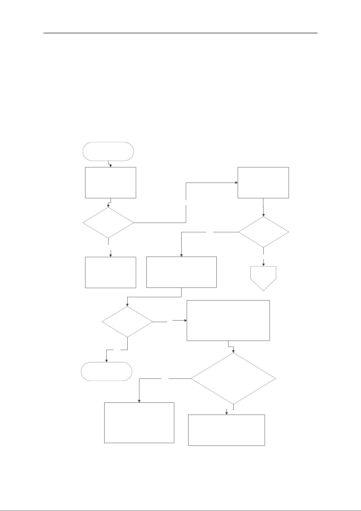
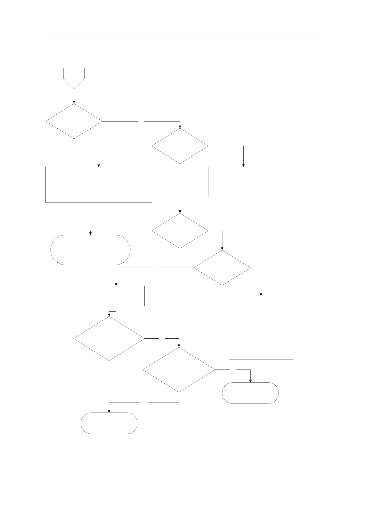
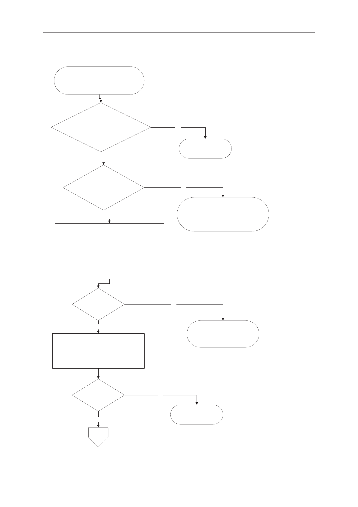
4.1. Phone is totally dead
This means that the phone doesn’t take current at all when the power switch S416 is
pressed or when the watchdog disable pin (X201 pin 11) is grounded. Used battery
voltage must be higher than 1,9 V. Otherwise the hardware of the switcher V105 and
CCONT (N100) will not operate reliable.
Phone is totally dead.
Measure Vb voltage at
C115
Yes
Measure Vdc_out
voltage
at Vibra pad E103
> 1,9 V
No
Failure in VB.
Check X101, X102 and
Jig or tester
Voltages OK?
Yes
Power doesn’t stay on.
Measure voltage at
2,85v>C117 (Vbb) > 2.7V
2,85V >C102 (VXO) > 2.7V
When PWR switch is pressed or
WDOGDISABLE is grounded.
Measure ”PWRON” voltage at R413
No
Yes
when pwr–switch (S416) is pressed or
Yes
WDDIS is grounded
(R424 connected to gnd).
Voltage less than 0,5V
(Will be low only during
power–up of CCONT
if power switch
is pressed.)
> 3.1V
No
Switcher
Figure 4–1
Issue 1 07/99
– PCB
Faulty:
– N100 circuit
– 32KHz or RFclk osc.
– Row0 on MAD
– Insufficient supply
capability of V105 circuit
No
Check R413, V410, S416, R423
N100
Check WDDIS line
Page 5
Page 6
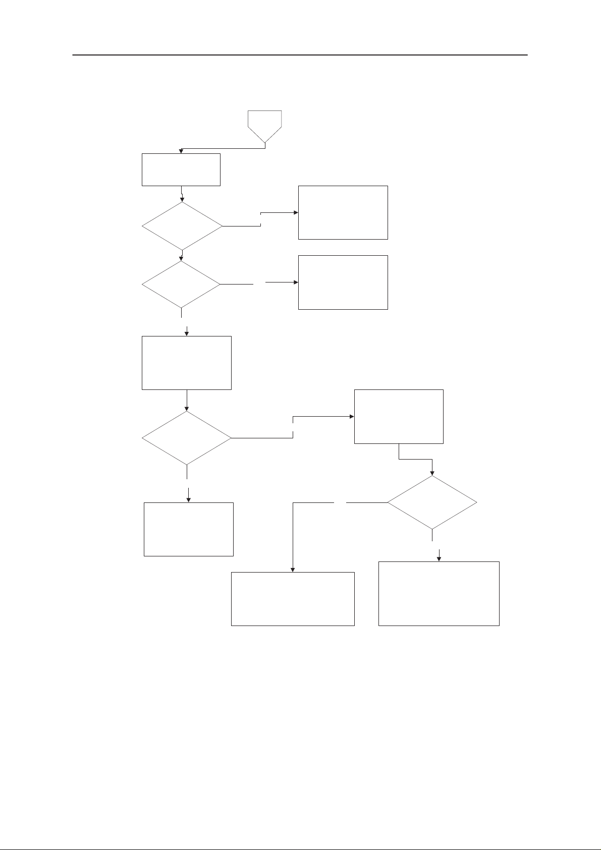
NSE–8/9
PAMS
Troubleshooting
Check voltage at
C109
less than 4,8 V
> 3.1 V
No
Switcher
No
Yes
Technical Documentation
Switcher feedback
somehow faulty
check circuitry arround
V105, V108, V109
Check L103 and
capacitors
C111 to C113
Check voltage at
pin 3 of V105
< 0,4 V
No
Check
L102, V101 and
circuitry arround
V109
Yes
Check capacitors C109
to
C113 and coil L103
Yes
Measure voltage
at V105 pin 15
app. 1.25 V
No
Check feedback circuitry
R102, R105, R112
and arround
V108. Or replace V105
Figure 4–2
4.2. Flash programming doesn’t work
The flash programming can be done via panel connector X201 or via service interface J100 - J105.
Page 6
Issue 1 07/99
Page 7

PAMS
NSE–8/9
Technical Documentation
In production, the first programming is done via panel connector X201. After this, the
panel connector is cut away, thus other flash programming must be done via service
interface J100 - J105.
The main differences between these are:
a) FLASH programming voltage is produced different way.
b) Signal routings are different.
The fault finding diagrams for flash programming are shown in Figure 4–3, Figure
4–4 and Figure 4–5.
In flash programming error cases the flash prommer can give some information
about a fault.
The fault information messages could be:
– MCU doesn’t boot
– Serial clock line failure
– Serial data line failure
– External RAM fault
– Algorithm file or alias ID don’t find
– MCU flash Vpp error
Troubleshooting
Issue 1 07/99
Page 7
Page 8
NSE–8/9
PAMS
Troubleshooting
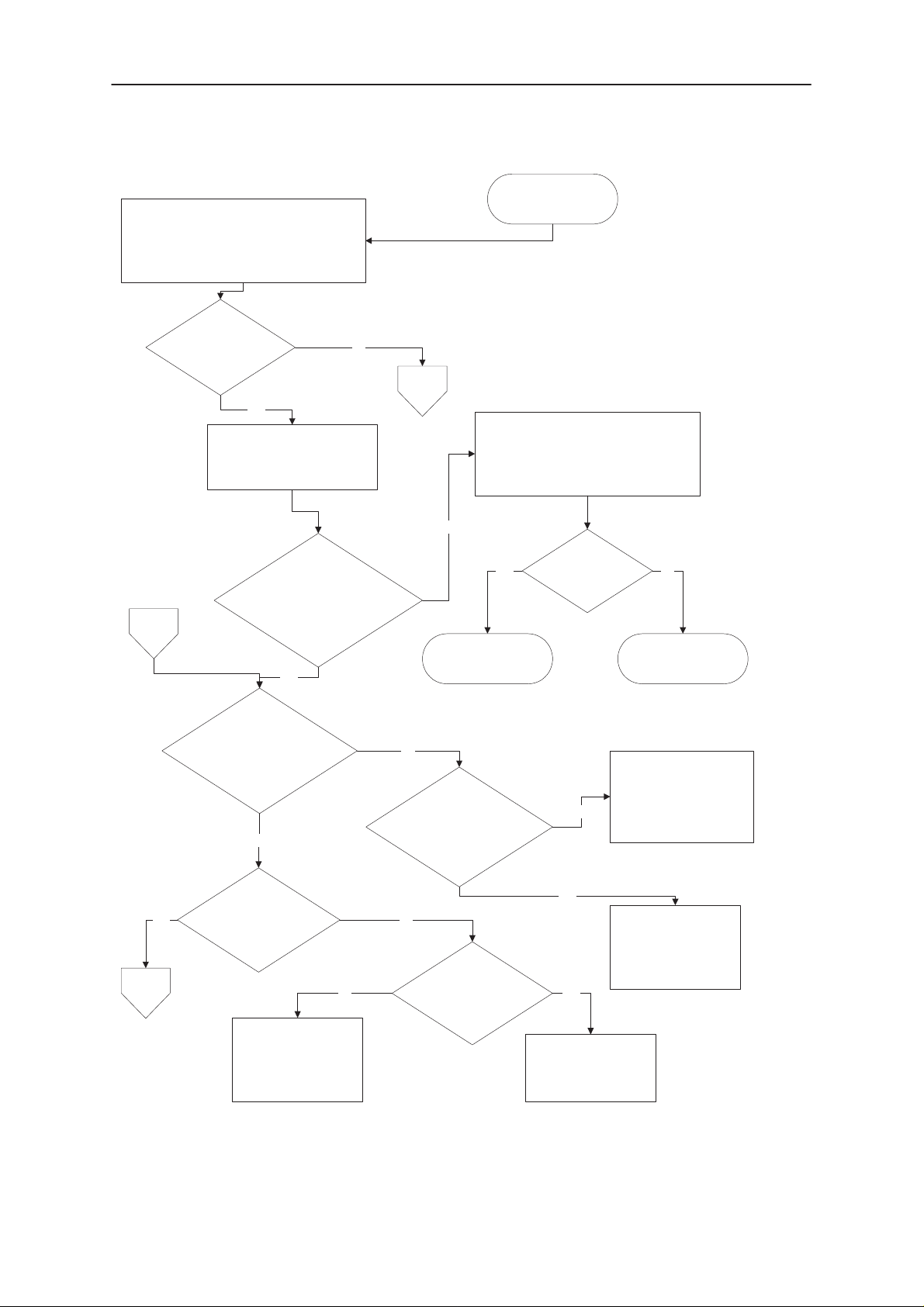
Check if fault information from
Prommer is one of the following:
a) MCU doesn’t boot
b) serial dataline failure
c) serial clock line failure
failure is one of the
above mentioned?
Connect watchdog disable
(WDDIS R424 ) to GND.
Technical Documentation
FLASH Programming
doesn’t work.
No
A
Yes
Check WDDIS line:
X201 pin 11 –> R424
No
C117 (Vbb) is typ 2.8V
C102 (VXO) is typ 2.8V
C
Master RESET
(PURX R303) is ”1” (2.8V)
after ca. 62ms
Yes
Yes
B
13MHz clock
C301 towards MAD
500mVpp min.
Yes
and
?
See section ”Phone is
totally dead”.
No
Check sleep clock
(R118 end towards CCONT )
32kHz square wave
No
No Yes
RFC 13MHz
800mV min.
V702 collector
Line OK?
No
Yes
NoYes
Faulty PCB
Check sleep clock circuit.
R121, R122, R123, R124,
C147, C148, C153, B100
and C149
Faulty N100 or
overloaded PURX line
Page 8
Check R727, V702,
R728, R714, G701
Figure 4–3
Check
R743 & C301
Issue 1 07/99
Page 9
PAMS
NSE–8/9
Technical Documentation
B
Check that the following lines are OK:
FCLK (M–BUS) line: J102, X201 pin 3 –> C306
FTX (fbus_tx) line: J103, X201 pin 1 –> C314
FRX (fbus_rx) line: J104, X201 pin 2 –> C305
(value on all should be 100 ohm)
Check also pull–up and –down resistors: R309, R310, R311
GND: J100, X201 pin 7 –> GND
OK? Repair or defect PCB
Troubleshooting
No
Yes
Check Service tool
TDS–7 & MJS–13
and
connections
Check that phone is
responding to flash
programming tool as
shown in fig. 4–3 to 4–5
MAD or FLASH faulty.
Figure 4–4
Issue 1 07/99
Page 9
Page 10
NSE–8/9
PAMS
Troubleshooting
A
External RAM fault?
Yes
Check pins of SRAM (D302)
Check control lines of SRAM:”MEMC(4:0)”
Technical Documentation
No
ID problem?
NO
Yes
Check type of FLASH
Check soldering of FLASH
Unknown fault. Check for noise on
communication lines
Try phone totally dead.
Check connection from
J105 to R307
Voltage at
R307 >1.7V & <3.6V
during flashing?
Yes
No
Yes
MCU FLASH Vpp
Error
No
Voltage at R307 12V +/–
5% during flashing?
Yes
Flashing from
X201?
Check
– that Vpp is not shorted by
R307 or C304.
– connection from R307 to
X201 pin 10
– Check Vpp
– Vbb=2.8V
– Vpp=12V +/– 5%
– Noise on MBUS/FBUS
lines
No
Vpp outside supported
YesNo
range.
Page 10
Defect FLASH or
flashing–SW has wrong
version.
Figure 4–5
Issue 1 07/99
Page 11

PAMS
NSE–8/9
Technical Documentation
Troubleshooting
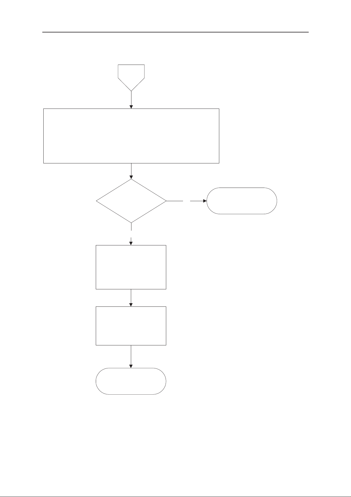
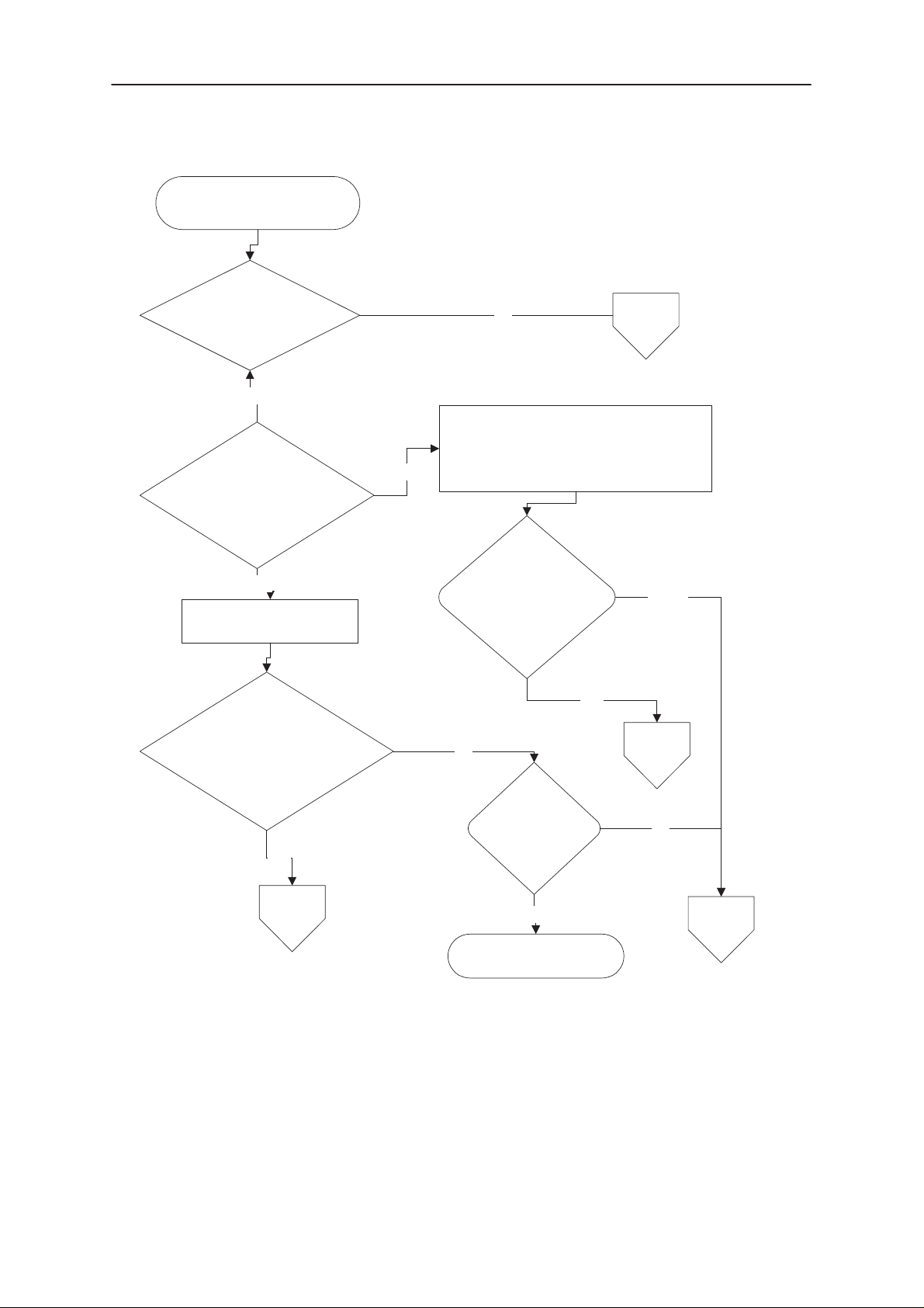
4.3. Power doesn’t stay on or phone is jammed
If this kind of fault has come after flash programming, there are most probably open
pins in ICs. The soldered joints of ICs: D300 (MAD2Pr1), D301 (FLASH), N100
(CCONT), D302 (SRAM) are useful to check at first.
Normally the power will be switched off by CCONT (N100) after 32 seconds, if the
watchdog of the CCONT can not be served by software.
Check watchdog is updated. Check that PWRON (at R413) is high and that
CCONTCSX (J337) toggles. In the normal case there is a short burst of pulses every
8 seconds.
The power off function of CCONT can be prevented by connecting a short circuit
wire from R424 to ground (Watchdog disabled).
Issue 1 07/99
Page 11
Page 12
NSE–8/9
PAMS
Troubleshooting
Power doesn’t stay on or
phone is jammed
C109 voltage <4,2V or
>3,1V ?
Check that
CCONTCSX J337
is pulsing and that PWRON
(R413) is high.
Is
Yes
Yes
Technical Documentation
No
Software is able to run in phone,
acknowledging watchdog.
If power is switched off after a few
seconds, check circuit arround V109.
Switcher
No
Connect R424 to GND
Check
VBB typ 2.8V at C117
and
VXO typ 2.8V at C102
and that they are
stable
Yes
C
Figure 4–6
Power doesn’t
stay on or phone is
jammed in idle
or call mode
Call
No
Is
Vdc_out stable
and within
limits?
Yes
N100 circuitry is faulty
No call
Switcher
Call
No
Switcher
Page 12
The LABEL “C” refers to Figure 4–3, The Label “Switcher” referes to Figure 4–2
Issue 1 07/99
Page 13
PAMS
NSE–8/9
Technical Documentation
Troubleshooting
4.4. Display Information: Contact Service
This fault means that software is able to run and thus the watchdog of CCONT
(N100) can be served.
Selftest functions are run when power is switched on and software is started to excute from flash.
If any of selftests is failed, contact service information will be shown on display.
a) Check Selftest status in WinTesla
b) Check that content of EEProm D303 and flash D301 is correct
c)
4.5. The phone doesn’t register to the network or phone doesn’t make a
call
If the phone doesn’t register to the network or the phone doesn’t make a call, the
reason could be either the baseband or the RF part.
The phone can be set to wanted mode by Wintesla service software and determinate if the fault is in RF or in baseband part (RF interface measurements).
The control lines for RF part are supplied both the System Asic (MAD2;D300) and
the RFI (Cobba_GJP; N200). MAD2Pr1 handles digital control lines ( like synthena,
TxP etc.) and Cobba handles analog control lines (like AFC, TxC etc.).
The DSP software is constructed so that operation states of DSP (MAD2Pr1) can be
seen in external flag (DSPXF) output pin J308.
After power up, DSP signals all completed functions by changing the state of the XF
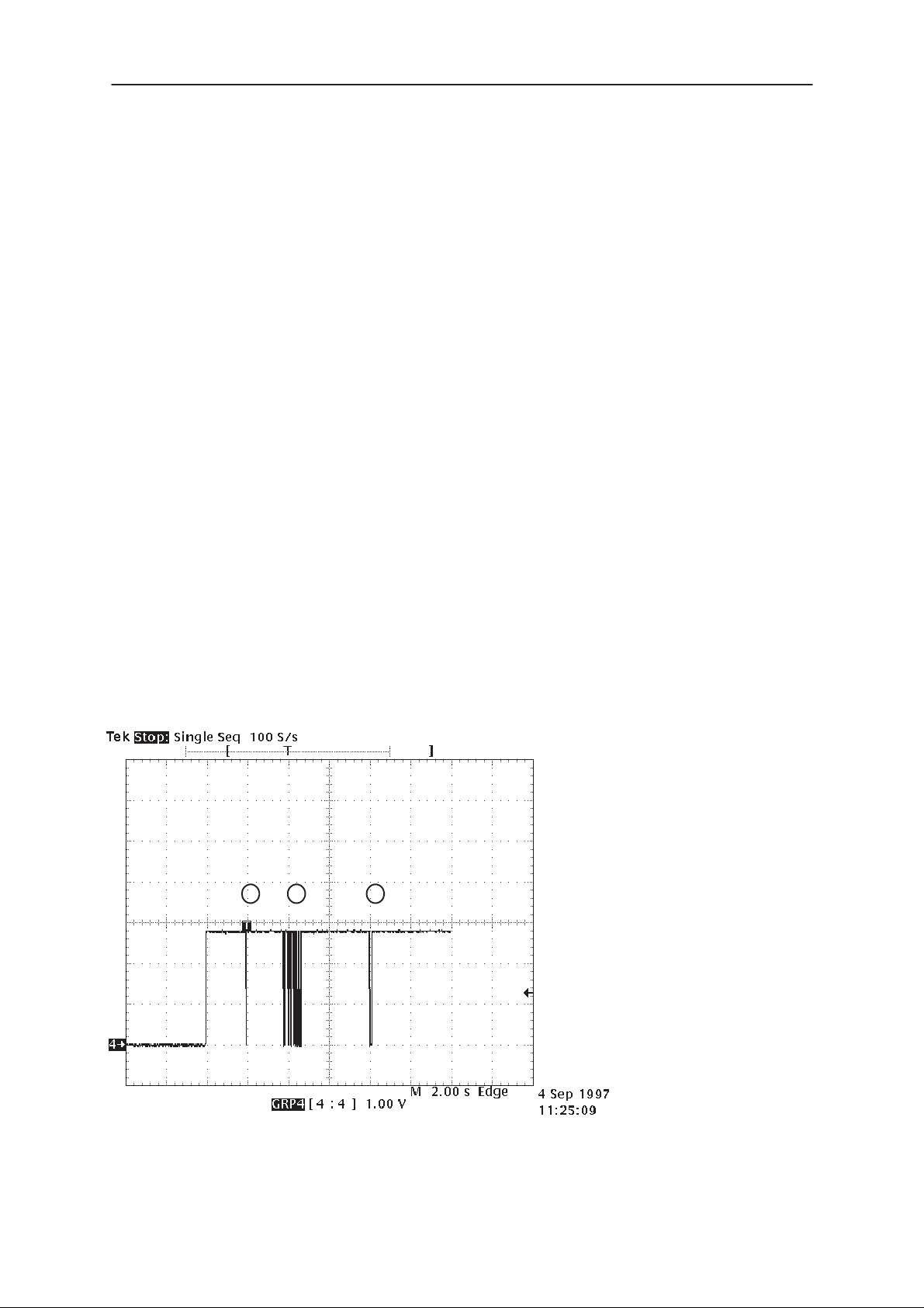
pin (see Figure 4–7, Figure 4–8, Figure 4–9 and Figure 4–10).
1. DSP initialization
done
2.Synchronization to
networknetwork
Network done
1 2 3
3. Registration to
Network done.
MAD2Pr1 pin D8
(DSPXF)
J308
The states of DSP (MAD2) after power on
Figure 4–7
Issue 1 07/99
Page 13
Page 14
NSE–8/9
PAMS
Troubleshooting
1
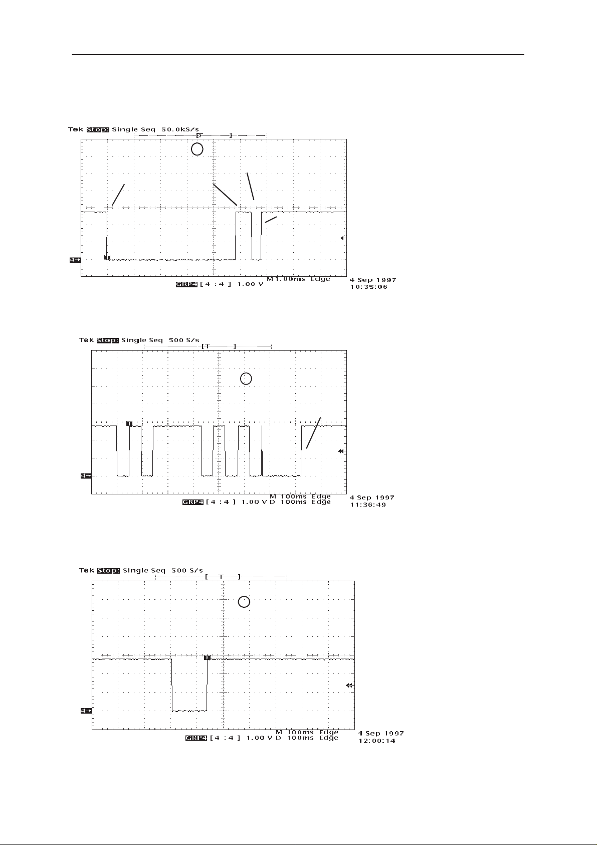
init
initialize
The states of DSP after power on
Figure 4–8
patch code
download
dsp
constants
download
initializatio
done
n
Technical Documentation
MAD2Pr1 pin D8
(DSPXF)
J308
PSW
search last PSW
channel
scan starts
The states of DSP after power on
Figure 4–9
send RACH
RACH OK
2
3
go SDCCH
imediate
OK
assigment
OK
synchronizatio
OK
n
MAD2Pr1 pin D8
(DSPXF)
J308
MAD2Pr1 pin D8
(DSPXF)
The states of DSP after power on
Figure 4–10
Page 14
J308
Issue 1 07/99
Page 15
PAMS
NSE–8/9
Technical Documentation
Phone doesn’t register to
the network or
phone doesn’t make a call
Analog supply
voltage to
COBBA is > 2.7V
(C218) and stable
?
Yes
Analog reference
to COBBA is 1.5V
(C205) and stable
?
Yes
Check:
Supply voltage Vcp (C132) > 4.8V
Supply voltage VRX_1 (C101) > 2.7V
Supply voltage VRX_2 (C104) > 2.7V
Supply voltage VSYN_2 (C103) > 2.7V
during the receiving slot
Supply voltage VTX (C125) > 2.7V
during the transmitting slot
Troubleshooting
No
Check N100
No
Check R207, C205, C123
and C124.
Check Vref and load on it
All OK?
Yes
Synthesizer lines:
SEna1 R724
SClk R722
SData R722
Pulses 0–>1 during receiving slot
All OK ?
Yes
D
No
Check N100, D300 and load in
RFon defective lines
No
Check D300
Figure 4–11
Issue 1 07/99
Page 15
Page 16

NSE–8/9
PAMS
Troubleshooting
D
RF control lines:
RxC (R725) 0–>2.3Vmax during receiving slot
AFC (C747) 0– 1.2V typ. during receiving slot
OK?
Yes
Analog data signals:
RxIP & RxIN 0–>1.5V DC during receiving slot
Recieved signal is biased to DC, amplitude
50mVpp nominal and frequency 13MHz
Technical Documentation
No
Check N200
OK?
Yes
RF control lines:
TxC (C700) 0–>2.3Vmax during transmit slot
TxP (R706) 0–>2.8V (logical signal) during
transmit slot
OK?
No
Check N200 if TxC fail
else
Check D300
No
Check N200 if DC fail
Yes
Analog data signals:
TxIN & TxIP (C709) 0–>0.8V DC during transmit slot
TxQN & TxQP (C708) 0–>0.8V DC during transmit slot
Transmit signal is biased to DC, amplitude 300mVpp
and frequency 64kHz
RF part
OK?
or
NoYes
Page 16
Check RF part Check N200
Figure 4–12
Issue 1 07/99
Page 17

PAMS
NSE–8/9
Technical Documentation
Troubleshooting
4.6. Plug in SIM card is out of order ( insert SIM card or card rejected).
The hardware of the SIM interface from MAD2Pr1 (D300) to the SIM connector
(X100) can be tested without SIM card.
When the power is switched on, all the used lines (VSIM, RST, CLK, DATA) rises up
to 3V one time and 5V tree times (see fig 5).
Thus ”Insert SIM card” faults can be found without SIM card.
The fault information ”Card rejected” means that ATR message (the first message is
always sent from card to phone) is sent from card to phone but the message is
somehow corrupted, data signal levels are wrong etc. or factory set values (stored to
the EEPROM) are not correct.
Issue 1 07/99
Page 17
Page 18

NSE–8/9
PAMS
Troubleshooting
Insert SIM card fault
VSIM (C137), DATA_0
(C140), SIMRST_0 (C139) and
SIMCLK_0 (C138) lines rise up to 3V on the
first puls and then 5V the next tree pulse
after power on with out simcard
No
Technical Documentation
Yes
Check soldring and springs
on X100
SIMIF(4:0) lines
SIMPWR (J321), SIMCardData (J325),
SIMCardRst (J324), SIMCLK (J323),
SIMIOC (J322)
rise to 2.8V after power on
No
Faulty D300
Yes
Faulty PCB, N100
Page 18
Figure 4–13
Issue 1 07/99
Page 19

PAMS
NSE–8/9
Technical Documentation
Card rejected fault
VSIM according
2.8Vmin (3V card) 3,2Vmax
4.5Vmin (5V card) 5,2Vmax
ATR data can be
seen at C140
Troubleshooting
to spec.
No
Faulty PCB, N100
Yes
No
Yes
ATR data can be seen
at J325 on D300
Yes
SIM_IOControl line (J322)
on D300 is ”1” during ATR
message
Yes
Check N100
Check X100, R115
No
Check N100
No
Check D300
Figure 4–14
Issue 1 07/99
Page 19
Page 20

NSE–8/9
PAMS
Troubleshooting
Technical Documentation
4.7. Audio fault.
Upon disassembly it is wise to check the spring contacts of the audio transducers and bottom connector
Uplink and downlink are
broken
Voltage on V202 pin 4
(HOOKDET) is 2.8V without
external audio devices
Yes
No
Check R226, R225,
R212, V202
Voltage on R200
(HEADDET) is 0,65V
without external audio
devices
Yes
Frequency at E200 on
(N200 PCMSclk) is 8kHz
square wave logical
level during call
Yes
Check for uplink and for
downlink broken
Figure 4–15
No
Check V200, R200,
R202
No
Check N200
Page 20
Issue 1 07/99
Page 21

PAMS
NSE–8/9
Technical Documentation
Uplink is broken
Voltage at C230 is 1.8V
Voltage at C231 is 0.3V
during call
Yes
DC–Voltage
on COBBA side of C258 & C259
is 1.4V
during call
Troubleshooting
No
Check:
microphone connections on X503
micbias components (C219, R214,
C220,R215, R216)
No
Yes
Audio voltage
(few millivolts)
on COBBA side of C258 & C259
during call
Yes
Check N200
Figure 4–16
Check N200 COBBA
No
Check C226, C229, R230,
R219, R220
MICRO–PHONE
and PCB
Issue 1 07/99
Page 21
Page 22

NSE–8/9
PAMS
Troubleshooting
Downlink broken
Voltage on C221 &
C222 is 1.4VDC
during call
Audio signal on L202
& L203 during call
when speaker should
emit sound
Technical Documentation
No
Check C221, C222,
C223, C224, B201, L202,
L203 and N200
Yes
No
Check L202, L203
B201, N200 & D300
Yes
Is earpiece
properly mounted
Yes
Check if springs are
damages
Figure 4–17
No
Repair or new module
Page 22
Issue 1 07/99
Page 23

PAMS
NSE–8/9
Technical Documentation
4.8. Charging Fault
Nothing happens when
charger is connected
Voltage level at R101 is
higher than 0.35V when
charger is connected
Yes
Troubleshooting
No
Check if pcb fuse F100 is
blown and
check X503, L100,L101
R100,R101 and C146
Check N100,
R104,N101,V114
Figure 4–18
and R137
Issue 1 07/99
Page 23
Page 24

NSE–8/9
PAMS
Troubleshooting
Voltage at C155 is about 0.5V,
power on, BTEMP value 47k
32Hz (fast charger) or
1Hz (slow charger) at
Technical Documentation
Display information:
Not charging
Yes
No
Check R125, C127,
C155 and N100
Yes
Check charg_ctrl
No
R142
Check N100 and R142
andR117
Yes
Is voltage the
same on both side on
switcher? C110 (3.2–4.1V)
and at V101 (2.0–3.0V)
Yes
Go to Switcher on fig4.2
No
voltage over R137
when charger is connected
ACP7~70mV
ACP9~190mV
Yes
Returning theCharger
Calibration with Wintesla
No
Check N101, R104, R137
V114 and C122
Page 24
Figure 4–19
Issue 1 07/99
Page 25

PAMS
NSE–8/9
Technical Documentation
RF Troubleshooting
Measurements should be done using Spectrum Analyzer with
high–frequency 500 ohm passive probe (LO–/reference frequencies and
RF–power levels) and Oscilloscope with a 10:1 probe (DC–voltages and
low frequency signals).
RF–section is mainly build from two ASICS CRFU3 (N600) and SUMMA
(N700), external filters, MMIC PA–modules (N500, N501) and two
synthesizers. For easier troubleshooting, this RF troubleshooting
document is divided into five sections: GSM Receiver, GSM Transmitter,
PCN Receiver, PCN Transmitter and Synthesizer parts. The tolerance is
specified for critical signals/voltages.
Before changing either of the ASIC’s, please check the following things:
The soldering and connections of pins of the ASIC’s are OK, supply
voltages are OK and the signals of the synthesizers are coming to ASIC’s.
This will prevent the unnecessary changing of the ASIC’s.
Troubleshooting
Please note that the grounding of the PA–module is directly below
PA–module so it is difficult to check. The PA–module is static discharge
sensitive! So ESD protection must be used when dealing with
PA–module (ground straps and ESD soldering irons). The PA’s are class 3
moisture sensitive so parts must be dry bake.
There are still a lot of discrete components (resistors, inductors and
capacitors) which troubleshooting is done just by checking that component
is soldered or it is not missing from PCB.
Issue 1 07/99
Page 25
Page 26
NSE–8/9
PAMS
Troubleshooting
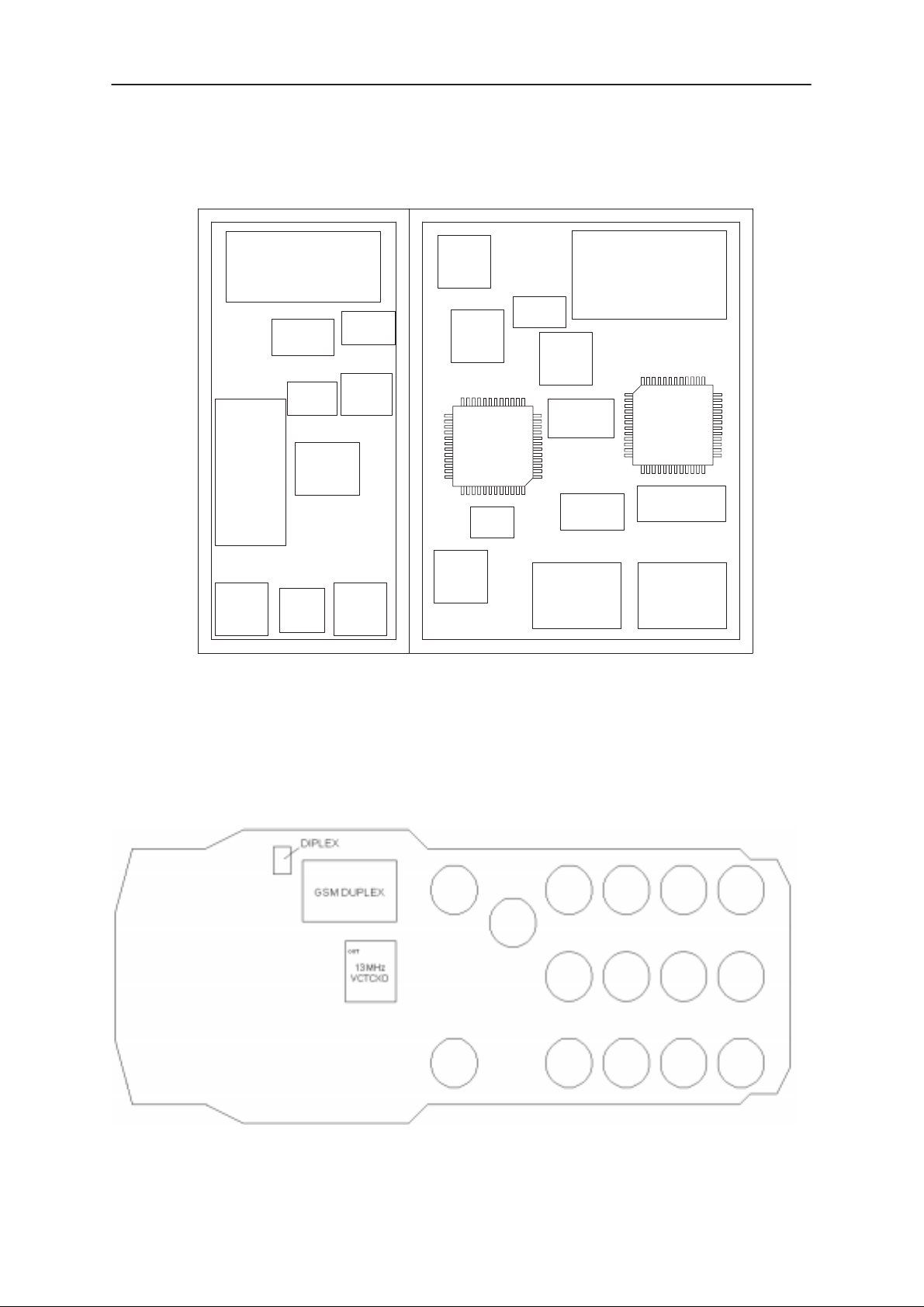
PCB Bottom view(GF7)
N500
PA
GSM
Z504
PCN
Switch
L503
Coupler
PCN
14
4
N502
PCN
Buffer
Z501
RX
PCN
1
PA
PCN
N501
Z502
TX
PCN
1
4
L500
Coupler
GSM
Z505
Diplexer
Z603
TX
PCN
Z601
TX
GSM
Z600
RX
GSM
25
N600
CRFU3
37
T600
PCN
Balun
Z602
RX
PCN
TX GSM
116MHz
13
1
Z702
TX PCN
232MHz
LO Filter
116MHz
RX
187MHz
G702
VHF VCO
Technical Documentation
71 MHz
SAW
Z700
1
37
N700
SUMMA
25
13MHz
Filter
Z701
G700
UHF VCO
OUT
Vcc
13
Vcc
OUT
PCB Top view (GF7 + GD7)
Page 26
Issue 1 07/99
Page 27

PAMS
NSE–8/9
Technical Documentation
Troubleshooting
2. GSM Receiver
2.1 . General instructions for GSM RX troubleshooting
Start WinTesla–Service–Software and
Select: P
Select: Te
roduct Alt+p
B
and b
SM g
G
sting Alt+e
F Controls r
R
R
X Continuous Alt+r
nt. Mode Ch: 60 Alt+o, 60
Co
Front E
Apply a 947.0 MHz (channel 60) –50 dBm signal to MJS–13
RF–connector. This signal is tracked through RX–path and will make the
troubleshooting of the RX easier.
nd On (if Front End is off,
2.2 . Path of the received GSM signal
This path defines the general route of the received signal:
Antenna, Diplexer (Z503), Duplexer (Z500), CRFU3 (LNA N600), GSM
Filter (Z600), CRFU3 (Mixer N600), SAW 71MHz Filter (Z700), SUMMA
(N700), 13Mhz Filter (Z701), SUMMA, COBBA_GJP (N200).
The related component number(s) are defined inside (.).
Alt+e)
Issue 1 07/99
Page 27
Page 28

NSE–8/9
PAMS
Troubleshooting
2.3. Fault finding chart for GSM receiver
.
Oscilloscope
SUMMA N700 pin 41 VREF Vdc = 1.5 Volt
SUMMA N700 pin 35 VRX_2 Vdc = 2.8 Volt
CRFU3 N600 pin 8, 47 VSYN_2 Vdc = 2.8 Volt
CRFU3 N600 pin 13, 33 VRX_1 Vdc = 2.8 Volt
OK
YES
Spectrum analyser
Verify 500 ohm passive probe
Measure at Diplexer (Z503)
antenna port
947 MHz
NO
Check
BaseBand
Technical Documentation
Pin = –50 dBm
Spectrum analyser
CRFU3 N600 pin 27
Pin = –54 dBm
Spectrum analyser
CRFU3 N600 pin 23
Pout = –35 dBm
.
YES
947 MHz
YES
947 MHz
YES
NO
NO
NO
Check
Spectrum analyser,
probe and signal
generator
Check
Diplexer (Z503)
Duplexer (Z500)
Check
CRFU3 (N600)
pin 24, BandSelect
pin 28, FraCtrl
Page 28
Issue 1 07/99
Page 29

PAMS
NSE–8/9
Technical Documentation
.
Spectrum analyser
CRFU3 N600 pin 18,19
947 MHz
NO
Pin = –47 dBm
YES
Spectrum analyser
CRFU3 N600 pin 15,16
71 MHz
Troubleshooting
Check
GSM Filter (Z600)
Pout = – 23 dBm
YES
Spectrum analyser
SUMMA N700 pin 37,38
71 MHz
Pin = –37 dBm
YES
Spectrum analyser
SUMMA N700 pin 30
13 MHz
NO
NO
Spectrum analyser
CRFU3 N600 pin 4
2036 MHz
Pin = –8 dBm
YES
Check
CRFU3 (N600)
Check
71 MHz SAW Filter
NO
Check
UHF Syntheziser
.
Issue 1 07/99
Page 29
Page 30

NSE–8/9
PAMS
Troubleshooting
.
Pout = –3 dBm
Spectrum analyser
SUMMA N700 pin 25
Pin = –22 dBm
13 MHz
YES
NO
NO
Technical Documentation
Check
SUMMA
Pin 36, RXC
Check
13 MHz Filter
Spectrum analyser
SUMMA N700 pin 23, 24
13 MHz
Pout = –3 dBm
Check
BaseBand
.
YES
YES
NO
Check
SUMMA
Page 30
Issue 1 07/99
Page 31

PAMS
NSE–8/9
Technical Documentation
Troubleshooting
3. PCN Receiver
3.1 . General instructions for PCN RX troubleshooting
Start WinTesla–Service–Software and
Select: P
Select: Te
roduct Alt+p
B
and b
CN p
P
sting Alt+e
F Controls r
R
R
X Continuous Alt+r
nt. Mode Ch: 700 Alt+o, 700
Co
Front E
Apply an 1842.8 MHz (MID channel) –50 dBm signal to MJS–13
RF–connector. This signal is tracked through RX–path and will make the
troubleshooting of the RX easier.
nd On (if Front End
3.2 . Path of the received PCN signal
This path defines the general route of the received signal:
Antenna, Diplexer (Z503), TX/RX Switch (Z504), PCN Filter (Z501),
CRFU3 (LNA N600), PCN Filter (Z602), CRFU3 (Mixer N600), LC 187
MHz Filter (L604), CRFU3 (Mixer N600), SAW 71MHz Filter (Z700),
SUMMA (N700), 13Mhz Filter (Z701), SUMMA, COBBA_GJP (N200).
The related component number(s) are defined inside (.).
is off, Alt+e)
Issue 1 07/99
Page 31
Page 32

NSE–8/9
PAMS
Troubleshooting
3.3 Fault finding chart for PCN receiver
.
SUMMA N700 pin 41 VREF Vdc = 1.5 Volt
SUMMA N700 pin 35 VRX_2 Vdc = 2.8 Volt
CRFU3 N600 pin 8, 47 VSYN_2 Vdc = 2.8 Volt
CRFU3 N600 pin 13, 33 VRX_1 Vdc = 2.8 Volt
OK
YES
Spectrum analyser
Verify 500 ohm passive probe.
Measure at Diplexer (Z503)
antenna port
1842.8 MHz
Oscilloscope
NO
BaseBand
Technical Documentation
Check
Pin = –50 dBm
YES
Spectrum analyser
CRFU3 N600 pin 34
1842.8 MHz
Pin = –53 dBm
YES
Spectrum analyser
CRFU3 N600 pin 38
1842.8 MHz
Pout = –35 dBm
NO
NO
NO
Check
Spectrum analyser,
probe and signal
generator
Check
Diplexer (Z503)
TX/RX Switch (Z504)
PCN Filter (Z501)
Check
CRFU3 (N600)
pin 24, BandSelect
pin 28, FraCtrl
.
Page 32
YES
Issue 1 07/99
Page 33

PAMS
NSE–8/9
Technical Documentation
. .
Spectrum analyser
CRFU3 N600 pin 42,43
1842.8 MHz
Pin = –47 dBm
NO
YES
Spectrum analyser
CRFU3 N600 pin 45,46
187 MHz
Check
PCN Filter (Z602)
Troubleshooting
Pout = –28 dBm
YES
Spectrum analyser
CRFU3 N600 pin 11,12
187 MHz
Pin = –31 dBm
YES
NO
NO
Spectrum analyser
CRFU3 N600 pin 4
2029.8 MHz
Pin = –7 dBm
YES
Check
CRFU3 (N600)
Check
187 MHz Filter
NO
Check
UHF Syntheziser
Spectrum analyser
CRFU3 N600 pin 15,16
71 MHz
. .
Issue 1 07/99
Page 33
Page 34

NSE–8/9
PAMS
Troubleshooting
.
Pout = –26 dBm
Spectrum analyser
SUMMA N700 pin 37,38
71 MHz
YES
NO
Spectrum analyser
CRFU3 N600 pin 9
116 MHz
Pin = –8 dBm
YES
Check
CRFU3 (N600)
L600, L601
Technical Documentation
Check
NO
VHF Syntheziser
Pin = –39 dBm
YES
Spectrum analyser
SUMMA N700 pin 30
13 MHz
Pout = –5 dBm
YES
Spectrum analyser
SUMMA N700 pin 25
13 MHz
NO
NO
Check
71 MHz SAW Filter
Check
SUMMA
pin 36, RXC
.
Page 34
Pin = –24 dBm
YES
NO
Check
13 MHz Filter
Issue 1 07/99
Page 35

PAMS
NSE–8/9
Technical Documentation
.
Spectrum analyser
SUMMA N700 pin 23, 24
13 MHz
Pout = –3 dBm
YES
Check
BaseBand
Troubleshooting
Check
NO
SUMMA
.
Issue 1 07/99
Page 35
Page 36

NSE–8/9
PAMS
Troubleshooting
Technical Documentation
4. GSM Transmitter
4.1 General instructions for GSM TX troubleshooting
Apply a RF–cable to the MJS–13 RF–connector to allow the transmitted
signal act as normal. RF–cable should be connected to measurement
equipment or to at least a 10–dB attenuator, otherwise the PA may be
damaged.
Start WinTesla–Service–Software and
Select: P
Select: Te
roduct Alt+p
B
and b
SM g
G
sting Alt+e
R
F Controls r
Power Level : BASE Alt+x, b
TX
ontinous Alt+c
TX C
ata Type: Random Alt+d, r
TX D
Chan
nel: 60 Alt+n, 60
pply Alt+a
A
4.2 . Path of the transmitted GSM signal
This path defines the general route of the transmitted signal:
COBBA_GJP (N200), SUMMA(N700), 116 MHz Filter (L703, L704, L708),
CRFU3 (Upconverter N600), GSM Filter (Z601), MMIC PA (N500),
Directional Coupler (L500), Duplexer (Z500), Diplexer (Z503), Antenna.
The related component number(s) are defined inside (.).
There is also power detection (V500) and power control circuits inside
SUMMA for transmitter power control.
Page 36
Issue 1 07/99
Page 37
PAMS
NSE–8/9
Technical Documentation
Troubleshooting
4.3 . Fault finding chart for GSM transmitter
. .
SUMMA N700 pin 41 VREF Vdc = 1.5 Volt
SUMMA N700 pin 27, 47 VTX Vdc = 2.8 Volt
SUMMA N700 pin 32 TXP Vdc > 2.5 Volt
CRFU3 N600 pin 8, 47 VSYN_2 Vdc = 2.8 Volt
CRFU3 N600 pin 39 VTX Vdc = 2.8 Volt
OK
YES
SUMMA N700 pin 1 TXQN Vac = 0.4 Vpp, Vdc = 0.8 V
SUMMA N700 pin 2 TXQP Vac = 0.4 Vpp, Vdc = 0.8 V
SUMMA N700 pin 3 TXIP Vac = 0.4 Vpp, Vdc = 0.8 V
SUMMA N700 pin 4 TXIN Vac = 0.4 Vpp, Vdc = 0.8 V
Oscilloscope
NO
Oscilloscope
Check
BaseBand
OK
YES
Spectrum analyser
SUMMA N700
pin 44, 45
116 MHz
Pout = –9 dBm
YES
Spectrum analyser
CRFU3 N600
pin 25, 26
116 MHz
. .
NO
NO
Check
SUMMA
VHF Synthesizer
Check
BaseBand
Issue 1 07/99
Page 37
Page 38

NSE–8/9
PAMS
Troubleshooting
. .
Check
Pin = –5 dBm
YES
Spectrum analyser
CRFU3 N600 pin 22
902 MHz
Pin = +9 dBm
NO
NO
116 MHz LC Filter
Spectrum analyser
CRFU3 N600 pin 4
2036 MHz
Technical Documentation
YES
Spectrum analyser
GSM PA N500 pin 1
902 MHz
Pin = 0 dBm
YES
WinTesla
TX_Data T ype: Random
TX Power Level: 10
NO
Pin = –8 dBm
YES
Check
CRFU3
Check
GSM Filter (Z601)
Alt+d,r
Alt+x,10
NO
Check
UHF Synthesizer
Spectrum analyser
GSM PA N500 pin 4
902 MHz
. .
Page 38
Issue 1 07/99
Page 39

PAMS
NSE–8/9
Technical Documentation
.
Pout = +21 dBm
YES
Spectrum analyser
MJS–13 RF–connector
902 MHz
Pout = +20 dBm
NO
NO
Troubleshooting
Check
GSM PA (N500)
Check
Power Loop
Detector (V500)
SUMMA N700 pin 31
SUMMA N700 pin 34 – TXC
Check
Directional Coupler (L500)
Duplexer (Z500)
Diplexer (Z503)
YES
GSM TX
OK
.
Issue 1 07/99
Page 39
Page 40

NSE–8/9
PAMS
Troubleshooting
Technical Documentation
5. PCN Transmitter
5.1 . General instructions for PCN TX troubleshooting
Apply a RF–cable to the MJS–13 RF–connector to allow the transmitted
signal act as normal. RF–cable should be connected to measurement
equipment or to at least a 10–dB attenuator, otherwise the PA may be
damaged.
Start WinTesla–Service–Software and
Select: P
Select: Te
roduct Alt+p
B
and b
CN p
P
sting Alt+e
F Controls r
R
TX
Power Level: BASE Alt+x, b
ontinous Alt+c
TX C
ata Type: Random Alt+d, r
TX D
nel: 700 Alt+n, 700
Chan
A
pply Alt+a
5.2 . Path of the transmitted PCN signal
This path defines the general route of the transmitted signal:
COBBA_GJP (N200), SUMMA (N700), 232 MHz SAW Filter (Z702),
CRFU3 (Upconverter N600), PCN Filter (Z603), PCN Buffer (N502), PCN
Filter (Z502), MMIC PA (N501), Directional Coupler (L500), TX/RX Switch
(Z504), Diplexer (Z503), Antenna.
The related component number(s) are defined inside (.).
There is also power detection (V500) and power control circuits inside
SUMMA for transmitter power control.
Page 40
Issue 1 07/99
Page 41
PAMS
NSE–8/9
Technical Documentation
Troubleshooting
5.3. Fault finding chart for PCN transmitter
. .
SUMMA N700 pin 41 VREF Vdc = 1.5 Volt
SUMMA N700 pin 27, 47 VTX Vdc = 2.8 Volt
SUMMA N700 pin 32 TXP Vdc > 2.5 Volt
CRFU3 N600 pin 8, 47 VSYN_2 Vdc = 2.8 Volt
CRFU3 N600 pin 39 VTX Vdc = 2.8 Volt
OK
YES
Oscilloscope
Check
NO
BaseBand
Oscilloscope
SUMMA N700 pin 1 TXQN Vac = 0.4 Vpp, Vdc = 0.8 V
SUMMA N700 pin 2 TXQP Vac = 0.4 Vpp, Vdc = 0.8 V
SUMMA N700 pin 3 TXIP Vac = 0.4 Vpp, Vdc = 0.8 V
SUMMA N700 pin 4 TXIN Vac = 0.4 Vpp, Vdc = 0.8 V
OK
YES
Spectrum analyser
SUMMA N700 pin 46
232 MHz
Pout = –11 dBm
NO
NO
Check
SUMMA
VHF Synthesizer
Check
BaseBand
YES
Spectrum analyser
CRFU3 N600 pin 35, 37
232 MHz
. .
Issue 1 07/99
Page 41
Page 42

NSE–8/9
PAMS
Troubleshooting
.
Pin = –11 dBm
Spectrum analyser
CRFU3 N600 pin 40
1747.8 MHz
Pin = 0 dBm
YES
YES
NO
NO
Technical Documentation
Check
232 MHz SAW Filter
Spectrum analyser
CRFU3 N600 pin 4
1979.8 MHz
Spectrum analyser
PCN Buffer N502 pin 1
1747.8 MHz
Pin = –7 dBm
YES
Spectrum analyser
PCN Buffer N502 pin 4
1747.8 MHz
NO
Pin = +6 dBm
YES
Check
CRFU3
Check
PCN Filter (Z603)
NO
Check
UHF Synthesizer
.
Page 42
Pout = +1 dBm
YES
NO
Check
PCN Buffer (Z502)
Issue 1 07/99
Page 43

PAMS
NSE–8/9
Technical Documentation
. .
Spectrum analyser
GSM PA N500 pin 1
1747.8 MHz
NO
Pin = –1 dBm
YES
WinTesla
TX_Data T ype: Random
TX Power Level: 10
Check
PCN Filter (N502)
Alt+d,r
Alt+x,10
Troubleshooting
Spectrum analyser
PCN PA N501 pin 4
1747.8 MHz
Pout = +8 dBm
YES
Spectrum analyser
Diplexer (Z503)
Antenna port
1747.8 MHz
Pout = +8 dBm
YES
NO
NO
Check
PCN PA (N501)
Check
Power Loop
Detector (V500)
SUMMA N700 pin 28
SUMMA N700 pin 34 – TXC
Check
Directional Coupler (L500)
TX/RX Switch (Z504)
Diplexer (Z503)
PCN TX
OK
. .
Issue 1 07/99
Page 43
Page 44

NSE–8/9
PAMS
Troubleshooting
Technical Documentation
6. Synthesizers
There are three oscillators generating the needed frequencies for
RF–section. 13 MHz reference oscillator, 464 MHz VHF VCO and UHF
VCO.
The frequency range for UHF VCO is GSM TX: 2012.4 ... 2061.6 MHz,
PCN TX: 1942.2 ... 2016.8 MHz,
GSM RX: 2012.4 ... 2061.6 MHz,
PCN RX: 1992.2 ... 2066.8 MHz.
6.1 . General instructions for Synthesizer troubleshooting
Start WinTesla–Service–Software and
Select: P
roduct Alt+p
and b
B
G
SM g
Select: Te
sting Alt+e
F Controls r
R
X Continuous Alt+r
R
Co
nt. Mode Ch: 60 Alt+o, 60
6.2 .. 13 MHz reference oscillator
The 13 MHz oscillator (G701) is controlled by COBBA_GJP (N200). This
13 MHz signal is pulse–shaped and connected to SUMMA (N700) and it is
also buffered, filtered and connected to MAD2 (D300).
6.3. VHF VCO
The 464 MHz VHF VCO (G702) signal is used to generate the 116 MHz–
and 232 MHz signals inside SUMMA. The 116 MHz signal is used in GSM
transmitter and in PCN receiver. The 232 MHz signal is used in PCN
transmitter.
Page 44
Issue 1 07/99
Page 45

PAMS
NSE–8/9
Technical Documentation
Fault finding table for VHF VCO
Troubleshooting
The fault finding is as described for UHF VCO with following exceptions:
UHF VCO VHF VCO
1 SUMMA N700 pin 21 changed to SUMMA N700 pin 12 Vdc = 1.8 ... 3.0 Volt
2 UHF VCO G700 changed to VHF VCO G702
3 SUMMA UHF PLL changed to SUMMA VHF PLL
4 UHF VCO G700 OUT–pin changed to VHF VCO G702 OUT–pin Pout > –3 dBm
The exceptions will be inside (.) in the fault finding chart for the UHF VCO.
6.4. UHF VCO
UHF VCO (G700) is used to generate the first injection for RX (GSM
2012.4 ... 2061.6 MHz, PCN 1992.2 ... 2066.8 MHz) and the final injection
for TX (GSM 2012.4 ... 2061.6 MHz, PCN 1942.2 ... 2016.8 MHz). The
output frequency of the module depends on the DC–control voltage
coming from SUMMA.
Issue 1 07/99
Page 45
Page 46

NSE–8/9
PAMS
Troubleshooting
6.5.
.
Fault finding chart –UHF VCO and 13 MHz ref. oscillator
Oscilloscope
SUMMA N700 pin 21
Vdc = 1.8 ... 3.0 Volt
Oscilloscope
SUMMA N700 pin 15
Technical Documentation
(12)
YES
OK
NO
Vac = >2 Vpp,
13 MHz
NO
Oscilloscope
VCTCXO G701 OUT–
pin
Vdc = 1.4 Volt
Vac = app. 1 Vpp,
13 MHz
NO
Oscilloscope
VCTCXO G701
VCC–pin
Vdc = 2.8 Volt
YES
YES
YES
VCTCXO G701 is OK
Check
Pulse–shaper D700
Check
VCTCXO G701
.
Page 46
NO
Issue 1 07/99
Page 47

PAMS
NSE–8/9
Technical Documentation
. .
Troubleshooting
Check
BaseBand
Oscilloscope
SUMMA N700 pin 41 VREF Vdc = 1.5 Volt
SUMMA N700 pin 13, 22 VCP Vdc > 4.0 Volt
SUMMA N700 pin 9, 16, 19 VSYN_2 Vdc = 2.8 Volt
UHF VCO G700 VCC–pin VSYN_2 Vdc = 2.7 Volt
SUMMA N700 pin 5
SUMMA N700 pin 6
SUMMA N700 pin 7
OK
YES
WinTesla
RX Burst Mode
Oscilloscope
=
=
=
OK
Check
NO
BaseBand
Synthesizer clock
Synthesizer data
Synthesizer enable
Check
NO
BaseBand
Issue 1 07/99
YES
..
Page 47
Page 48

NSE–8/9
PAMS
Troubleshooting
.
Spectrum analyser
C608
2036 MHz
Technical Documentation
Spectrum analyser
SUMMA pin 8
464 MHz
.
.
Check
NO
VHF VCO G702
Pout > –10 dBm
.
YES
Check
Pout > –10 dBm
NO
UHF VCO G700
YES
Spectrum analyser
SUMMA N700 pin 18
1018 MHz
YES
Pin > –10 dBm
UHF (VHF) Synthesizer
seems to be OK
Check
discrete components
NO
Check
CRFU3
.
.
Page 48
Issue 1 07/99
 Loading...