

Page 1

Customer Care Solutions
Technical Documentation
T roubleshooting Instructions
ISSUE 1 02/2004 COMPANY CONFIDENTIAL 1
Copyright © 2003 Nokia. All Rights Reserved.
Page 2

RM-4/RM-5
CCS Technical Documentation Troubleshooting Instructions
[This page left intentionally blank]
2 COMPANY CONFIDENTIAL ISSUE 1 02/2004
Copyright © 2003 Nokia. All Rights Reserved.
Page 3
RM-4/RM-5
Troubleshooting Instructions CCS Technical Documentation
Table of Contents
Page No
Baseband troubleshooting .............................................................................................5
Baseband testpads .......................................................................................................5
Component side (PWB backside) ............................................................................. 5
Display connector (PWB front side) ........................................................................ 5
Close up of testpads .................................................................................................. 6
Fault Finding Charts ...................................................................................................... 8
Phone is dead .............................................................................................................. 8
Flash programming does not work .............................................................................. 9
Power doesn't stay on or phone is jammed ............................................................... 10
Display information: "Contact Service" ....................................................................11
No network or no call ................................................................................................ 12
SIM related faults ......................................................................................................13
SIM-Card rejected ..................................................................................................14
Audio related faults ................................................................................................... 15
No sound in earpiece ..............................................................................................15
Microphone does not work .....................................................................................16
Headset microphone does not work ........................................................................ 17
Headset earpiece does not work .............................................................................17
No sound from IHF or headset ...............................................................................18
Handsfree speaker does not work ........................................................................... 19
Charging faults .......................................................................................................... 20
General RF Troubleshooting ....................................................................................... 23
RF Key component placement ..................................................................................24
General Instructions for GSM900 RX Troubleshooting ........................................... 26
Troubleshooting Chart for GSM900 Receiver .......................................................27
General Instructions for GSM1800 RX Troubleshooting ......................................... 29
Troubleshooting Chart for GSM1800Receiver ......................................................30
Measurement points in the receiver ........................................................................ 31
RM-4/RM-5 Transmitter troubleshooting ................................................................. 33
Measurement points for the transmitter .................................................................. 33
General instructions for RM4/RM-5 GSM TX troubleshooting ............................... 34
PCN Transmitter General instructions for PCN TX troubleshooting ....................... 36
Synthesizer ................................................................................................................ 37
26 MHz Reference Oscillator (VCXO ) .................................................................37
VCO ........................................................................................................................37
Troubleshooting diagram for PLL Synthesizer ......................................................38
Phone fails after power on ......................................................................................39
Measurement points at the VCXO .......................................................................... 39
Measurement points at the PLL/VCO ....................................................................40
Manual Alignment using Phoenix ............................................................................... 41
RX calibration ...........................................................................................................41
GSM1800 RX calibration .........................................................................................42
RX channel select filter ............................................................................................. 43
RX Band Filter Response.......................................................................................... 44
Tx Power tuning ........................................................................................................ 45
ISSUE 1 02/2004 COMPANY CONFIDENTIAL 3
Copyright © 2003 Nokia. All Rights Reserved.
Page 4

RM-4/RM-5
CCS Technical Documentation Troubleshooting Instructions
TX power tuning GSM ...........................................................................................45
TX power tuning PCN ............................................................................................ 48
I/Q tuning .................................................................................................................. 50
RF control .................................................................................................................52
Call testing ................................................................................................................53
General instructions for RM-4/5 FM radio Troubleshooting ...................................... 54
Location of testpoints ................................................................................................ 54
Phoenix control ......................................................................................................... 54
Fault finding guide ....................................................................................................56
4 COMPANY CONFIDENTIAL ISSUE 1 02/2004
Copyright © 2003 Nokia. All Rights Reserved.
Page 5
RM-4/RM-5
Troubleshooting Instructions CCS Technical Documentation
Baseband troubleshooting
Baseband testpads
Component side (PWB backside)
Figure 1: Component side (PWB backside)
Display connector (PWB front side)
Figure 2: Display connector (PWB front side)
ISSUE 1 02/2004 COMPANY CONFIDENTIAL 5
Copyright © 2003 Nokia. All Rights Reserved.
Page 6
RM-4/RM-5
CCS Technical Documentation Troubleshooting Instructions
Close up of testpads
Production test pads for programming FLASH and service functions (J396)
RFBUS RF I/Q signals
6 COMPANY CONFIDENTIAL ISSUE 1 02/2004
Copyright © 2003 Nokia. All Rights Reserved.
Page 7
RM-4/RM-5
Troubleshooting Instructions CCS Technical Documentation
FLASH
CBUS / DBUS / FBUS / MBUS / SLEEPX / PURX / AUDIO
SHUTDOWN
ISSUE 1 02/2004 COMPANY CONFIDENTIAL 7
Copyright © 2003 Nokia. All Rights Reserved.
Page 8
RM-4/RM-5
CCS Technical Documentation Troubleshooting Instructions
Fault Finding Charts
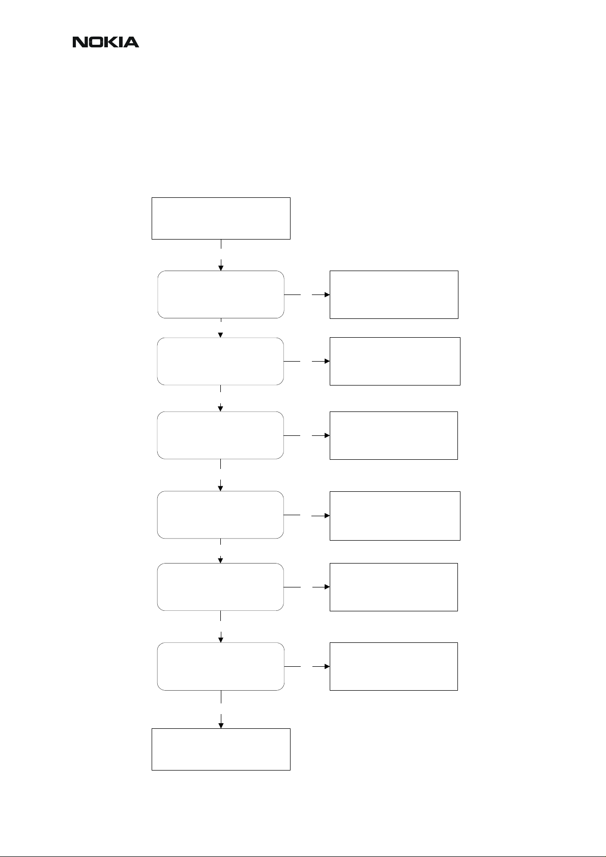
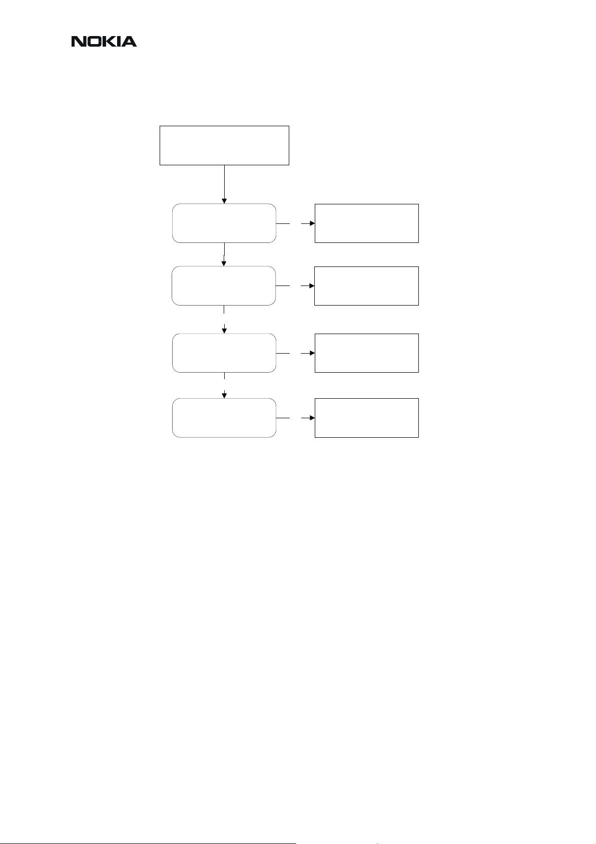
Phone is dead
Nominal battery voltage is 3.7 VDC. The phone (UEM) wont startup at battery/supply levels below 3.1 VDC. The software will turn off the phone at 3.21 VDC.
Phone is dead
Yes
X105
VBAT = 3,6VDC
Yes
L260,L261,L262,L263,L264,L265
C260,C261,C262,C263,C264,C265
Voltage = 3,6VDC
Yes
J404
Sleep-clock is
32.768 kHz, 1,8Vpp
Yes
J402
PURX = 1,8VDC,
1 sec. after power-key
is pressed
Yes
C227
VR3 = 2,78VDC
No
No
No
No
No
Check :
X105
Check :
L260,L261,L262,L263,L264,L265
C260,C261,C262,C263,C264,C265
Check :
B200, C209, C210, PWB. Else
defective D200*
Check :
PWB.
Else defective D200*
Check :
C227, PWB.
Else defecti v e D200*
Yes
26 MHz clock min. 300mVACpp,
R426
probe Cin=10-13 pF/10M
Yes
No
Check :
C227, PWB.
Else defecti v e D200*
Check :
D450 (Flash).
Else defective D200*
8 COMPANY CONFIDENTIAL ISSUE 1 02/2004
Copyright © 2003 Nokia. All Rights Reserved.
Page 9
RM-4/RM-5
Troubleshooting Instructions CCS Technical Documentation
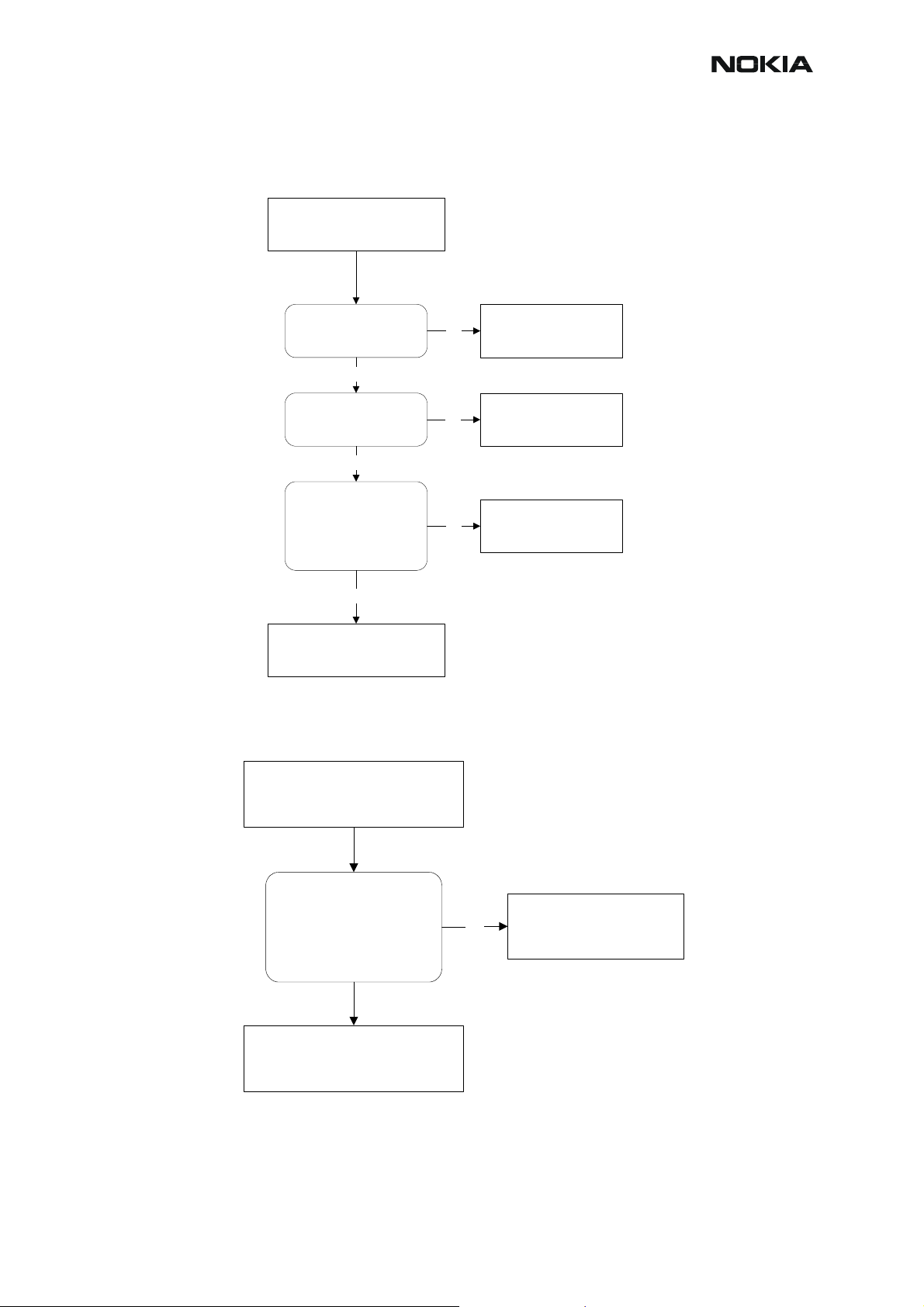
Flash programming does not work
.
Flash prgramming
do not work
Error from prommer:
"Phone doesn't set
FBUS_TX line low"
Yes
J396, R108
Check connection between
pad 1,2 & 3 on J396
and R108
Yes
J409, J410, J411, J412
Voltage level at 1,8VDC
Yes
Try reading MCU ID
with Phoenix.
Reading OK?
Yes
Try reading Flash ID
with Phoenix.
Reading OK?
Yes
No
No
No
No
Check :
R108, PWB
Check :
PWB.
Else defective D200*
Check :
PWB.
Else defictive D400*
Check :
Replace D450
Reflash phone
ISSUE 1 02/2004 COMPANY CONFIDENTIAL 9
Copyright © 2003 Nokia. All Rights Reserved.
Page 10
RM-4/RM-5
CCS Technical Documentation Troubleshooting Instructions
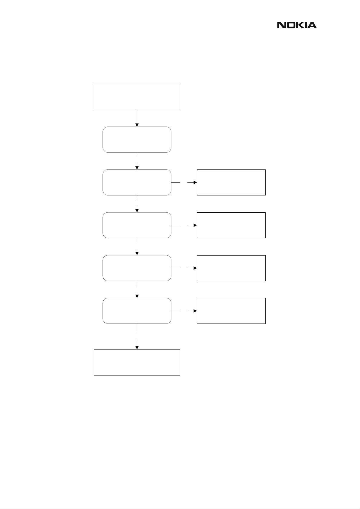
Power doesn't stay on or phone is jammed
If for some reason the MCU does not service the watchdog register within the UEM, the operations watchdog will run out after approximately 32 seconds and should initiate a reset.
Power doesn't stay on,
or phone is jammed
J404
Sleep clock = 32.768 kHz,
1.8Vpp
Yes
J402
PURX = 1,8VDC,
1 sec. after power-key is
pressed
Yes
UI functionality,
and keys react
to pressure?
Yes
R426
26 MHz clock min.
300mVACpp,
probe Cin=10-13 pF/10M
Yes
No
No
No
No
Check :
B200, C209, C210, PWB.
Else defective D200*
Check :
PWB.
Else defective D200*
Check :
D450, Keymat,
Lightguide, PWB.
Else defective D400*
Check :
C420, C426, R420,
R426, N600(Mjoelner)
Reflash phone
10 COMPANY CONFIDENTIAL ISSUE 1 02/2004
Copyright © 2003 Nokia. All Rights Reserved.
Page 11
RM-4/RM-5
Troubleshooting Instructions CCS Technical Documentation
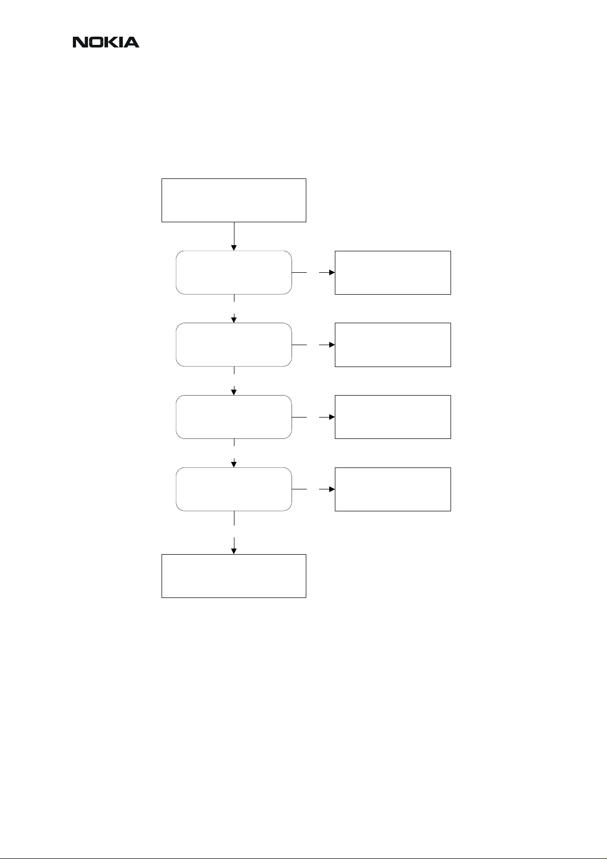
Display information: "Contact Service"
This message shows when internal self-tests have failed. If any of the following cases fails the
display will show the message: "Contact Service".
The lineup below has no chronological order. Use common sense and experience to decide
which test case to start error hunting at.
Display shows
"Contact Service"
Yes
EarDa & MicDa
between
UPP and UEM?
MBUS interface
between
UPP and UEM?
AuxDa & UEMInt
between
UPP and UEM?
SleepX & SleepClk
between UPP & UEM?
TXI/QD & RXI/QD?
SIM interface between
UPP & UEM
No
Check :
PWB.
Else defective D200*
or D400*
Key is stucked
Flash checksum
y ASIC version vs. compilation flag, PMM checksum
y PMM validity
y Warrenty Information State
y SIM-Lock
Check :
A-cover, Keymat, Lightguide,
PWB.
Reflash phone
Check :
PWB.
Else defective D450 (FLASH)
ISSUE 1 02/2004 COMPANY CONFIDENTIAL 11
Copyright © 2003 Nokia. All Rights Reserved.
Page 12
RM-4/RM-5
CCS Technical Documentation Troubleshooting Instructions
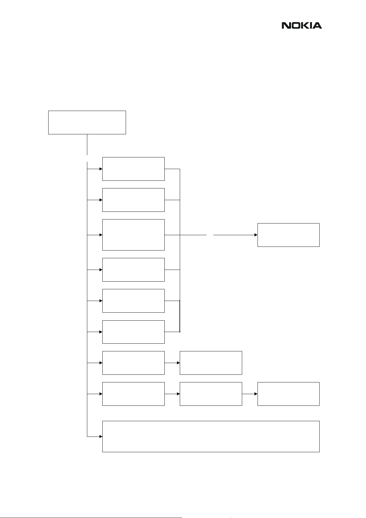
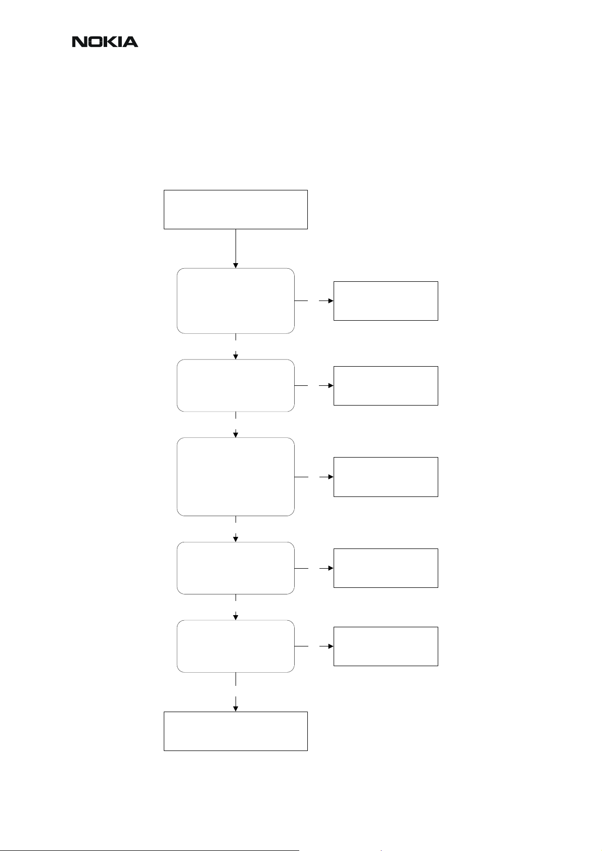
No network or no call
If the phone doesn't register to the network, the fault can be in either BB or RF. Only few signals
can be tested since several signals is 'buried' in one or more of the inner layers of the PWB.
First of all check that it’s not a SIM LOCK causing the error by using a Test-SIM card and connect the phone to a tester.
Phone do not register to
network
or phone cannot make a call
C222, C223, C224, C225,
C226, C227
Voltage = ~2,78VDC
All during GSM frame-
call mode.
Use TXP on C646 as trigger
Yes
C230, C231
Voltage = ~1,35VDC
All during GSM frame (call mode)
Use TXP on C646 as trigger
Yes
J421, J422, J423
Check RF serial bus during
GSM-frame :
Logic HIGH = 1,8VDC
Logic LOW = 0VDC
RFBUSCLK (J421),
RFBUSDA (J422),
RFBUSEN1X (J423)
Yes
R601, R603
Check analog signals during
GSM-frame (RX slot):
RXIP/N (R601) = 0-1,45VDC
RXQP/N (R603) = 0-1,45VDC
No
No
No
No
C222,C223, C224, C225,
C226, C227, PWB.
Else defective D200 or D400*
C230, C231, PWB.
Else defective
D200* or D400*
Else defective D200*
Else defective D200*
Check :
Check :
Check :
PWB.
or D400*
Check :
PWB.
or D400*
Yes
R610, R611
Check analog signals during
GSM-frame (TX slot):
TXIP/N (R610) = 1-1,75VDC
TXQP/N (R611) = 1-1,75VDC
Yes
No
Check :
R610, R611,PWB.
Else defective D200*
or D400*
Check RF
12 COMPANY CONFIDENTIAL ISSUE 1 02/2004
Copyright © 2003 Nokia. All Rights Reserved.
Page 13
RM-4/RM-5
Troubleshooting Instructions CCS Technical Documentation
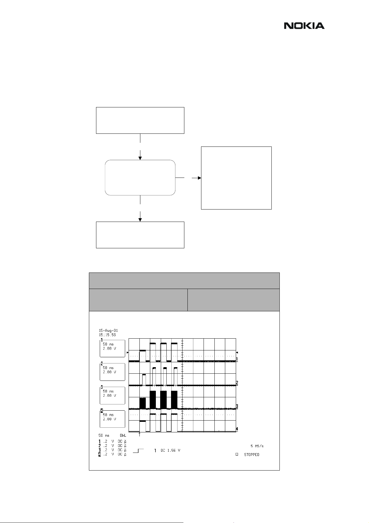
SIM related faults
The hardware of the SIM interface from UEM (D200) to the SIM connector (X387) can be tested
without a SIM card. When the power is switched on the phone first check for a 1.8V SIM card
and then a 3V SIM card. The phone will try this four times, whereafter it will display ”Insert SIM
card”.
Display shows :
"Insert SIM Card"
Yes
Check :
X387
Verify that phone checks for
1,8V-SIM, and t h en 3V -SIM
during power-up.
(See illustration below)
Yes
No
X387, R386, PWB.
Else defective D200*
Message can also appear if
BSI signal from battery is not
present or only working
intermittently .
Please check BSI.
SIM Interface OK
Check for SIM voltage during power-up
Ch1: VSIM
Ch2: RESET
Ch3: CLOCK
Ch4: DATA
ISSUE 1 02/2004 COMPANY CONFIDENTIAL 13
Copyright © 2003 Nokia. All Rights Reserved.
Page 14
RM-4/RM-5
CCS Technical Documentation Troubleshooting Instructions
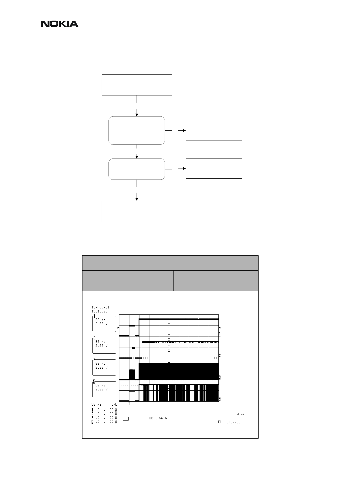
SIM-Card rejected
Display shows :
"SIM Card Rejected"
Yes
VSIM = min. 1,6V(1,8V Card)
X387
VSIM = min. 2,8V(3V Card)
(See illustration below)
Yes
X387
ATR data can be seen at
SIM data pin.
Yes
SIM Interface OK
No
No
Check :
R386, PWB.
Else defective D200*
Check :
X387, R386, PWB.
For reference a picture with normal SIM power-up is shown below.
Normal SIM power-up sequence
Ch1: VSIM
Ch2: RESET
Ch3: CLOCK
Ch4: DATA
14 COMPANY CONFIDENTIAL ISSUE 1 02/2004
Copyright © 2003 Nokia. All Rights Reserved.
Page 15
RM-4/RM-5
Troubleshooting Instructions CCS Technical Documentation
Audio related faults
Earpiece = Speaker mounted in display assy.
IHF = Integrated handsfree. Speaker mounted in back cover (D-cover).
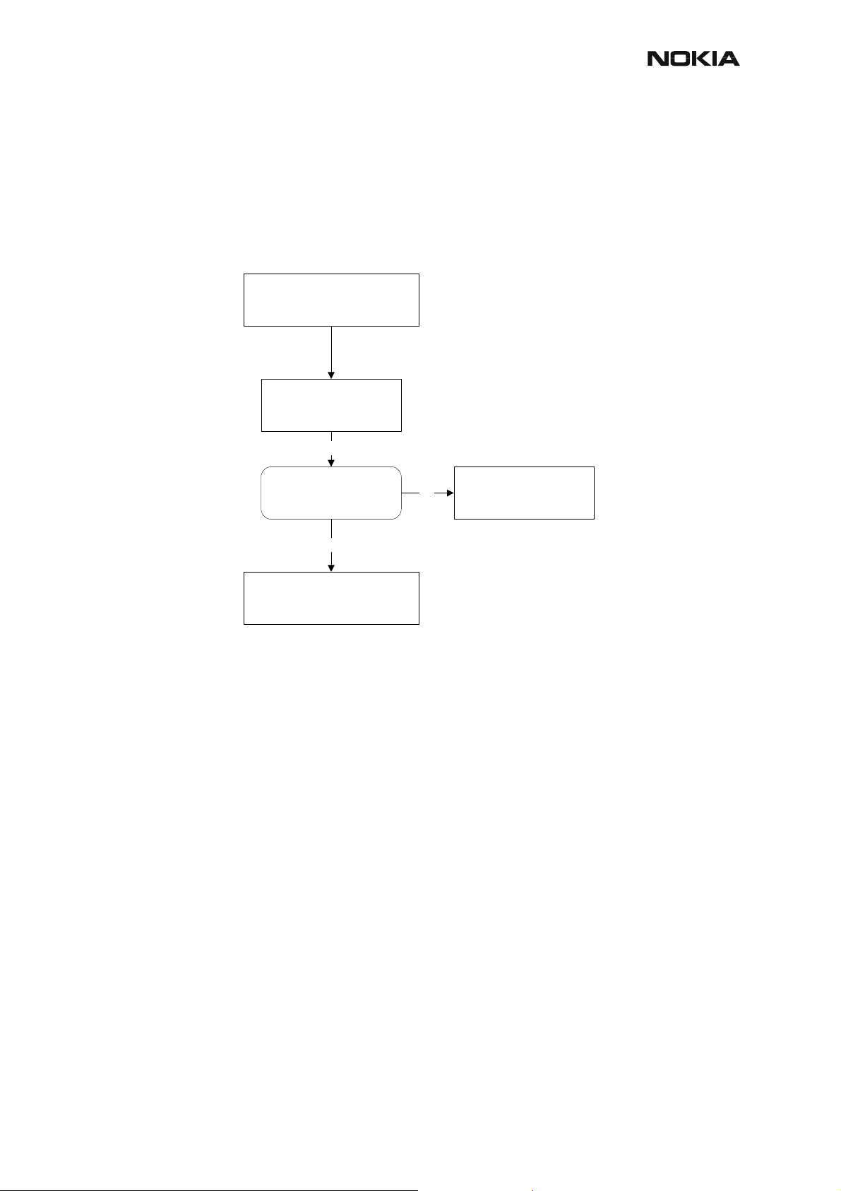
No sound in earpiece
Earpiece do not work
Replace :
Earpiece
Error still present
Z150, R161
Check Z150, R161 is
working correctly
(no short/open-circuit)
Yes
Defective D200*
(or PWB error)
No
Replace :
Z150 / R161
ISSUE 1 02/2004 COMPANY CONFIDENTIAL 15
Copyright © 2003 Nokia. All Rights Reserved.
Page 16
RM-4/RM-5
CCS Technical Documentation Troubleshooting Instructions
Microphone does not work
Microphone do not work and
it's not a mechanical
problem
Z100
Check Z100 is
working correctly
(no short/open-circuit)
C101,C102 & C103
Check for short-circuit.
Error still present
R165
Check voltage level on
R165 towards UEM (bias)
= 2,1V
Yes
R153
Check voltage level on
R153 towards mic-lines (bias)
= 1,0V - 1,4V
No
No
No
No
Replace :
Z100
Replace :
C101, C102, C103
Check :
R165, C168, PWB.
Else defctive D200*
Check :
R152, R153, R155, R157,
R164, C151, C152, C153,
C154, PWB.
16 COMPANY CONFIDENTIAL ISSUE 1 02/2004
Copyright © 2003 Nokia. All Rights Reserved.
Page 17
RM-4/RM-5
Troubleshooting Instructions CCS Technical Documentation
Headset microphone does not work
Headset microphone do not
work and it's not a
mechanical problem
Check voltage level on R166
Check voltage level on R151
R166
towards UEM (bias) = 2,1V
R151
towards UEM (bias)
= 1,0V - 1,4V
R154, R156, R160,
R162, R168, C172,
C170, C173, C174,
Z101
Check XMIC line to UEM
(D200)
Error still present
Defective D200*
Headset earpiece does not work
Yes
Yes
No
No
No
Replace :
R166 and/or Z101
Check :
R166, R151, C171
Replace :
Defective component
Headset earpiece do not
work.
R183, Z102, C123,
C124
Check that components are
working correctly
Defective D200*
No
Replace :
R183 and/or Z102, C123,
C124
ISSUE 1 02/2004 COMPANY CONFIDENTIAL 17
Copyright © 2003 Nokia. All Rights Reserved.
Page 18
RM-4/RM-5
CCS Technical Documentation Troubleshooting Instructions
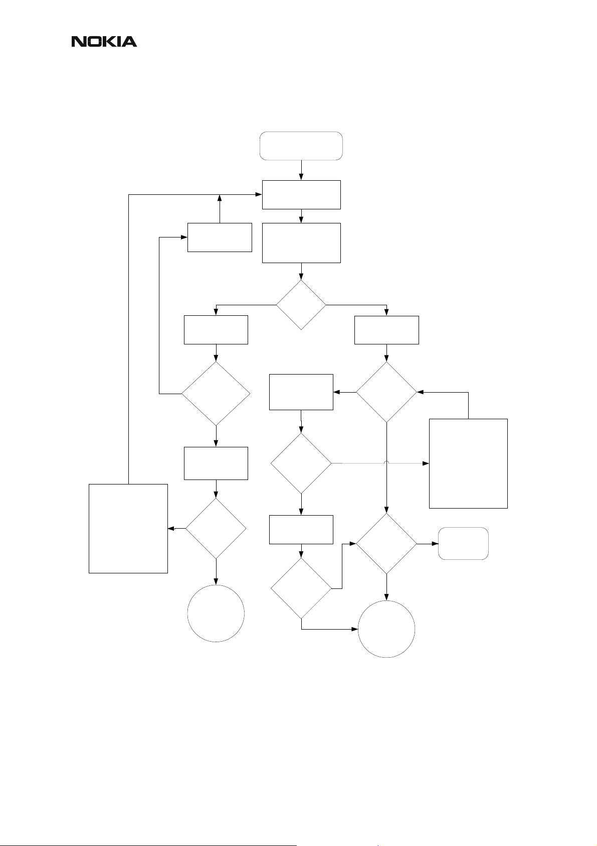
No sound from IHF or headset
START
Insert headset
(working reference)
Clean PWB and system
connector (replace if
defect)
Risk of decreased phone
performance if PWB
pads are corroded or
badly scratched. Reliable
repair might be
impossible.
Clean/Replace
system connector
Check system
connector switch
Yes
Is there a
malfunction or
dirt in the
switch?
No
Check PWB and
connector springs
on the system
connector
Yes
Dirty, dusty,
scratched or
corroded?
Go to "Headset
earpiece do not
work".
No
Turn on radio and tune in
to a station (using menu
navigation). Increase
volume with navigation
key.
No
Sound in
headset?
Check IHF pads on
PWB and spring
contacts on IHF
speaker
Dirty, dusty,
scratched or
corroded?
No
Change IHF
speaker.
(working reference)
Yes
Sound in
IHF?
No
Yes
Yes
Enable radio
through loudspeaker
No
Sound in
IHF?
Yes
Distorted
sound?
Yes
Go to "Handsfree
speaker do not
work".
Clean PWB and IHF
speaker contact springs.
Risk of decreased phone
performance if PWB
pads are corroded or
badly scratched. Reliable
repair might be
impossible.
No
IHF OK
18 COMPANY CONFIDENTIAL ISSUE 1 02/2004
Copyright © 2003 Nokia. All Rights Reserved.
Page 19

RM-4/RM-5
Troubleshooting Instructions CCS Technical Documentation
Handsfree speaker does not work
A FM signal generator at 88 MHz (1KHz LF) and 99% modulation was used a s “radio station ”.
START
Check input on N180.
(R181/R159) Fig.1
input ok?
Input ok
Check VBAT on C182
voltage
above 3.2
VDC?
yes
Check TP J150
Boomer is activated if signal
is high.
no
no
(possible PWB or N180 solder
Check :
C159, C180, C181, C183,
C186, R159, R181
(D200)
Are you sure the module is
powered on?
error)
Check output at IHF pads
(J151 / J152) Fig.2
Output ok?
yes
Assemble
phone.
FIG.1 - Input of N180
no
Check/Replace :
L180, L181, C 189, C190
Signal high?
(1.8 VDC)
yes
Check output on N180
(at C184 / C185) Fig.2
Output looks
OK?
yes
no
Check :
Short circuit of N180, PWB
error or D400. (make sure IHF
is activated in software!).
no
Check/Replace :
C184, C185, C189, C190
(change N180)
FIG.2 - Output of N180
ISSUE 1 02/2004 COMPANY CONFIDENTIAL 19
Copyright © 2003 Nokia. All Rights Reserved.
Page 20

RM-4/RM-5
CCS Technical Documentation Troubleshooting Instructions
Charging faults
Phone is OFF - battery is
completely empty
(<=3,1VDC)
and no current from
charger when connected
L100
VCHAR > 2,1VDC
Yes
Defective D200*
Display info when
charger is connected :
"Not charging"
R206
Voltage on R206 towards
D200 is ~0,8VDC
when power is connected.
(BSI must be 75K)
Yes
R207
Voltage (use scope) on R207
towards D200 is ~0,9VDC at
peak.
(BSI must be 47K)
No
No
No
F100, L100, V100, C100,
R200, R100 (NTC resistor)
System-connector.
X105, R202, R206, C240.
X105, R202, R207, C220.
Check :
Check :
Check :
Yes
R200
Voltage on R200 towards
D200 same as VBAT voltage
Yes
R200
Voltage rises slowly on
R200 towards D200 when
charger is connected.
Yes
No
No
Check :
R200, PWB.
Else defective D200*v
Check :
PWB.
Else defective D200*
Check :
PWB
20 COMPANY CONFIDENTIAL ISSUE 1 02/2004
Copyright © 2003 Nokia. All Rights Reserved.
Page 21

RM-4/RM-5
Troubleshooting Instructions CCS Technical Documentation
Phone is ON or OFF - battery
nominal voltage (~3,7VDC)
and no current from
charger when connected
L100
VCHAR > 3,7VDC
Yes
Defective
D200 or D400*
No
Check :
F100, L100, V100, C100,
R200, System-connect o r .
ISSUE 1 02/2004 COMPANY CONFIDENTIAL 21
Copyright © 2003 Nokia. All Rights Reserved.
Page 22

RM-4/RM-5
CCS Technical Documentation Troubleshooting Instructions
[This page left intentionally blank]
22 COMPANY CONFIDENTIAL ISSUE 1 02/2004
Copyright © 2003 Nokia. All Rights Reserved.
Page 23

RM-4/RM-5
Troubleshooting Instructions CCS Technical Documentation
General RF Troubleshooting
Two types of measurements are used in the following. It will be specified if the measurement
type is "RF" or "LF".
• RF measurements are done with a Spectrum Analyser and a highfrequency 500 ohm passive probe, for example HP54006A. (Note that
when measuring with the 500 ohm probe the signal will be around 20 dB
attenuated. The values in the following will have these 20 dB subtracted
and represent the real value seen on the spectrum analyser).
Note that the testjig have some losses which must be taken into consideration when calibrating
the test system.
• LF (Low frequency) and DC measurements should be done with a 10:1
probe and an oscilloscope. The probe used in the following is 10 Mohm,
8pF passive probe. If using another probe then bear in mind that the
voltages displayed may be slightly different.
Always make sure the measurement set-up is calibrated when measuring RF parameters on
the antenna pad. Remember to include the loss in the module repair jig when realigning the
phone.
Most RF semiconductors are static discharge sensitive.
plied during repair (ground straps and ESD soldering irons). Mjoelner and Bifrost is moisture
sensitive so parts must be pre-baked prior to soldering.
Apart from key-components described in this document there are a lot of discrete components
(resistors, inductors and capacitors) for which troubleshooting is done by checking if soldering
of the component is done properly and checking if the component is missing from PWB. Capacitors can be checked for short-circuiting and resistors for value by means of an ohmmeter,
but be aware in-circuit measurements should be evaluated carefully.
So, ESD protection must be ap-
ISSUE 1 02/2004 COMPANY CONFIDENTIAL 23
Copyright © 2003 Nokia. All Rights Reserved.
Page 24

RM-4/RM-5
CCS Technical Documentation Troubleshooting Instructions
RF Key component placement
Figure 3: RF key components
Table 1: RF component placement
N600 Mjoelner RF IC
Z601 PCN RX SAW
Z602 EGSM RX SAW
Z603 EGSM TX SAW
B600 26 MHz crystal
G600 VCO (4.0 GHz UHF VCO )
N700 Power Amplifier (PA)
Z700 RX/TX switch
24 COMPANY CONFIDENTIAL ISSUE 1 02/2004
Copyright © 2003 Nokia. All Rights Reserved.
Page 25

RM-4/RM-5
Troubleshooting Instructions CCS Technical Documentation
Refer to the picture below for measuring points at the UEM (D200).
Figure 4: Supply points at UEM (D200)
Figure 5: Supply point at Mjoelner (N600)
ISSUE 1 02/2004 COMPANY CONFIDENTIAL 25
Copyright © 2003 Nokia. All Rights Reserved.
Page 26

RM-4/RM-5
CCS Technical Documentation Troubleshooting Instructions
General Instructions for GSM900 RX Troubleshooting
Connect the phone to a PC with the module repair jig.
Start Phoenix and establish connection to the phone
Phoenix commands
RF Controls .Band GSM 900 RX .Continuous mode
Channel 37 .AGC 8 FEG ON + 46 dB
The setup should now look like this:
Figure 6: GSM900 RF Controls window
26 COMPANY CONFIDENTIAL ISSUE 1 02/2004
Copyright © 2003 Nokia. All Rights Reserved.
Page 27

RM-4/RM-5
Troubleshooting Instructions CCS Technical Documentation
Troubleshooting Chart for GSM900 Receiver
Figure 7: EGSM Receiver Troubleshooting chart
Apply -55dBm
942.4 MHz
offset 67.71kHz
from generator
to
antenna conn
YES
Oscilloscope
at RX i/Q
signal 588mVpp
DC offset 1.35V
Freq.67.71kHz
YES
EGSM
chain
OK
Check RX/TX
switch at
RX900
Z700
-56dBm
YES
Spectrum analyzer
EGSM SAW filter
Z602
output
-65dBm
YES
Spectrum analyzer
check signal after
inductors
L602 and L603
-65DbM
NO NO
NO
Oscilloscope
check
VC1 and VC2
at Z700
Signal = 0V
NO
YES
Check
RX/TX
switch
Check
SAW filter
Z602
Check
Inductor
L603, L602
Check Mjoelner
YES
YES
Oscilloscope
VRX 2.7V
Check Mjoelner
serial
interface
NO
Check
Baseband
ISSUE 1 02/2004 COMPANY CONFIDENTIAL 27
Copyright © 2003 Nokia. All Rights Reserved.
Page 28

RM-4/RM-5
CCS Technical Documentation Troubleshooting Instructions
By measuring with an oscilloscope at RXIP or RXQP on a working GSM 900 receiver this picture should be seen.
Signal amplitude peak-peak 789 mV
DC offset 1.2 V
Figure 8: RX900 I/Q signal waveform
28 COMPANY CONFIDENTIAL ISSUE 1 02/2004
Copyright © 2003 Nokia. All Rights Reserved.
Page 29

RM-4/RM-5
Troubleshooting Instructions CCS Technical Documentation
General Instructions for GSM1800 RX Troubleshooting
Connect the phone to a PC with the module repair jig.
Start Phoenix and establish connection to the phone
Phoenix commands
RF Controls .Band GSM 1800 RX .Continuous mode
Channel 700 .AGC 8 FEG ON + 46 dB
The setup should now look like this:
Figure 9: GSM1800 RF control window
ISSUE 1 02/2004 COMPANY CONFIDENTIAL 29
Copyright © 2003 Nokia. All Rights Reserved.
Page 30

RM-4/RM-5
CCS Technical Documentation Troubleshooting Instructions
Troubleshooting Chart for GSM1800Receiver
Figure 10: GSM1800 receiver Troubleshooting chart
Apply -55dBm
1842.8 MHz
offset 67.71kHz
from generator
to
antenna conn
YES
Oscilloscope
at RX i/Q
signal 588mVpp
DC offset 1.35V
Freq.67.71kHz
YES
EGSM
chain
OK
Check RX/TX
switch at
RX1800
Z700
-56dBm
YES
Spectrum analyzer
EGSM SAW filter
Z601
output
-65dBm
YES
Spectrum analyzer
check signal after
inductors
L601 and L611
-65DbM
NO NO
NO
Oscilloscope
check
VC1 and VC2
at Z700
Signal = 0V
NO
YES
Check
RX/TX
switch
Check
SAW filter
Z602
Check
Inductor
L603, L602
Check Mjoelner
YES
YES
Oscilloscope
VRX 2.7V
Check Mjoelner
serial
interface
NO
Check
Baseband
30 COMPANY CONFIDENTIAL ISSUE 1 02/2004
Copyright © 2003 Nokia. All Rights Reserved.
Page 31

RM-4/RM-5
Troubleshooting Instructions CCS Technical Documentation
XIP or RXQP on a working GSM 1800 receiver this picture should be seen.
Signal amplitude peak-peak 460 mV
DC offset 1.2 V
Figure 11: RX1800 I/Q signal waveform
Measurement points in the receiver
Figure 12: RX measurements point at the RX/TX Switch - Z700
ISSUE 1 02/2004 COMPANY CONFIDENTIAL 31
Copyright © 2003 Nokia. All Rights Reserved.
Page 32

RM-4/RM-5
CCS Technical Documentation Troubleshooting Instructions
Figure 13: Measurements points at the RX-Filters – Z601/Z602
Figure 14: RX I/Q Signals, Baseband shielding can UEM (D200)
32 COMPANY CONFIDENTIAL ISSUE 1 02/2004
Copyright © 2003 Nokia. All Rights Reserved.
Page 33

RM-4/RM-5
Troubleshooting Instructions CCS Technical Documentation
RM-4/RM-5 Transmitter troubleshooting
Measurement points for the transmitter
Figure 15: TX measurement points in the PA (N700) shielding can
Figure 16: TX measurement points in Mjolner (N600) shielding can
ISSUE 1 02/2004 COMPANY CONFIDENTIAL 33
Copyright © 2003 Nokia. All Rights Reserved.
Page 34

RM-4/RM-5
CCS Technical Documentation Troubleshooting Instructions
General instructions for RM4/RM-5 GSM TX troubleshooting
Apply a RF-cable to the RF-connector to allow the transmitted signal act as normal. RF-cable
should be connected to measurement equipment or to at least a 10-dB attenuator, otherwise
the PA may be damaged.
Start Phoenix-Service-Software and establish a connection to the phone e.g. FBUS.
Select File and Product.
Select: Maintenance, Testing and RF Controls
Band: GSM 900
Active Unit: TX
Tx Power Level: 19
Tx Data Type: All 1
Your screen should look like:
Figure 17: GSM900 RF controls window
Measure the output power of the phone; it should be around 32.5 dBm.
Remember the loss in the jig; around 0.3 dB.
34 COMPANY CONFIDENTIAL ISSUE 1 02/2004
Copyright © 2003 Nokia. All Rights Reserved.
Page 35

RM-4/RM-5
Troubleshooting Instructions CCS Technical Documentation
Figure 18: VPCTRL_G and TXC signal
ISSUE 1 02/2004 COMPANY CONFIDENTIAL 35
Copyright © 2003 Nokia. All Rights Reserved.
Page 36

RM-4/RM-5
CCS Technical Documentation Troubleshooting Instructions
PCN Transmitter General instructions for PCN TX troubleshooting
Apply a RF-cable to the RF-connector to allow the transmitted signal act as normal. RF-cable
should be connected to measurement equipment or to at least a 10-dB attenuator, otherwise
the PA may be damaged.
Start Phoenix-Service-Software and establish a connection to the phone e.g. FBUS.
Phoenix commands
RF Controls .Band GSM 1800 RX .Continuous mode
Channel 700 .AGC 14 FEG ON + 24 dB
Your screen should look like:
Figure 19: RF controls window
Measure the output power of the phone; it should be around 28.5 dBm. Remember the loss in
the jig; around 0.7 dB.
36 COMPANY CONFIDENTIAL ISSUE 1 02/2004
Copyright © 2003 Nokia. All Rights Reserved.
Page 37

RM-4/RM-5
Troubleshooting Instructions CCS Technical Documentation
Synthesizer
There is only one PLL synthesizer generating Local Oscillator frequencies for both RX and TX
in both bands (PCN and EGSM). The VCO frequency is divided by 2 for PCN operation or by
4 for EGSM operation inside the Mjoelner IC.
26 MHz Reference Oscillator (VCXO )
The 26 MHz oscillator is located in the Mjoelner IC (N600). The coarse frequency for this oscillator is set by an external crystal (B600). The reference oscillator is used as a reference frequency for the PLL synthesizer and as the system clock for BaseBand. The 26MHz signal is
divided by 2 to achieve 13MHz inside the UPP IC (D400).
The 26 MHz signal from the VCXO can be measured by probing R425 (must be measured on
the UPP side of R425 i.e. the end not
700mVpp. Frequency of this oscillator is adjusted by changing the AFC-register inside the
Mjoelner IC. This is done via the Mjoelner serial interface.
Example Signal Measured at VCXO output (R425)
connected to C425). The level at this point is approx.
Figure 20: VCXO 26 MHz waveform
VCO
The VCO is an ASIC with all the frequency determining parts inside.
In order to reduce the requirements of the tuning voltage and coverage of the VCO, the VCO
core is composed of four VCOs in parallel. This VCO circuit enables a very wide tuning range
of 3.4 - 4.0 GHz .
ISSUE 1 02/2004 COMPANY CONFIDENTIAL 37
Copyright © 2003 Nokia. All Rights Reserved.
Page 38

RM-4/RM-5
CCS Technical Documentation Troubleshooting Instructions
Troubleshooting diagram for PLL Synthesizer
Figure 21: PLL Troubleshooting diagram
38 COMPANY CONFIDENTIAL ISSUE 1 02/2004
Copyright © 2003 Nokia. All Rights Reserved.
Page 39

RM-4/RM-5
Troubleshooting Instructions CCS Technical Documentation
Phone fails after power on
If the phone stops working a short time after the power is turned ON, a possible reason for this
could be that the 26MHz system clock signal is not getting to the UPP clock-input in BaseBand.
In this case check the following:
1 Turn on the phone and check
2 VCXO Power supply (C620) = 2.7V
3 VCXO output (R420 – end not connected to C425) is 26MHz and approx. 700mVpp
If this is not the case check the reference crystal (B600) and Mjolner (N600) as well as R420,
R426, C420, C426.
Measurement points at the VCXO
Figure 22: Measurement point for VCXO supply
Figure 23: Measurement point for VCXO output
ISSUE 1 02/2004 COMPANY CONFIDENTIAL 39
Copyright © 2003 Nokia. All Rights Reserved.
Page 40

RM-4/RM-5
CCS Technical Documentation Troubleshooting Instructions
Measurement points at the PLL/VCO
Figure 22: Measurement point for PLL
40 COMPANY CONFIDENTIAL ISSUE 1 02/2004
Copyright © 2003 Nokia. All Rights Reserved.
Page 41

RM-4/RM-5
Troubleshooting Instructions CCS Technical Documentation
Manual Alignment using Phoenix
In Phoenix select connection Fbus and Product Gemini. If you power up the board before selecting Fbus, it works without any error messages.
Use Jig or other device for RF and bus connection. Attenuation in the probe alone is 0.5dB for
900 and 1dB for 1800. Use CMD55 or other suitable device. Default channels are 37 for
GSM900 and 700 for GSM1800. The alignments and calibrations must be performed in the order shown to give reliable results.
The way to save data to the phone and to load data from the phone is made different in the
various tunings. Always look what is shown in the windows regarding these issues and act accordingly.
To vary a selected parameter you can use + and – key or in some cases directly type the new
value. + and – steps the value for every press. Repeat function seems not to work. In I/Q you
can use the side arrows.
RX calibration
Select Maintenance, Tuning, RX Calibration
Select Band: GSM 900
Select Automatic and follow the prompts
The result should be like the shown:
Figure 23: RX calibration window
ISSUE 1 02/2004 COMPANY CONFIDENTIAL 41
Copyright © 2003 Nokia. All Rights Reserved.
Page 42

RM-4/RM-5
CCS Technical Documentation Troubleshooting Instructions
GSM1800 RX calibration
1 The existing data in the phone is shown
2 Calibrate, and the new data is shown
3 Stop, and the little window pops up where you can select to save or not
4 Select GSM1800 in the top bar and repeat at channel 700
Figure 24: GSM1800 RX calibration window
1 The existing data in the phone is shown
2 Calibrate, and the new data is shown
3 Stop, and the little window pops up where you can select to save or not
42 COMPANY CONFIDENTIAL ISSUE 1 02/2004
Copyright © 2003 Nokia. All Rights Reserved.
Page 43

RM-4/RM-5
Troubleshooting Instructions CCS Technical Documentation
RX channel select filter
1 Select Maintenance, Tuning, Rx Channel Select Filter Calibration.
2 Press Start and you can select to load values from the phone or not.
3 Press AutoTune
4 Press Stop and you can select to save values to the phone or not to..
Figure 25: RX channel selection window
Note: This calibration requires no input signal
ISSUE 1 02/2004 COMPANY CONFIDENTIAL 43
Copyright © 2003 Nokia. All Rights Reserved.
Page 44

RM-4/RM-5
CCS Technical Documentation Troubleshooting Instructions
RX Band Filter Response
1 Select Maintenance, Tuning, Rx Band Filter Response Compensation
2 Press Start, Read from PM area and you can select to load values from the phone
or not
3 Press Manual Tuning
4 Set the Signal generator according to the pop-up windows
5 When finished press Stop, Write to PM area and you can select to save values to
the phone or not
6 Repeat for GSM1800
Figure 26: RX Band filter response window
Note: This calibration requires a lot of different frequencies from the generator. If you have a signal
generator with a frequency list option you can with advantage use Auto Tuning (Dwell should be
around 10ms).
44 COMPANY CONFIDENTIAL ISSUE 1 02/2004
Copyright © 2003 Nokia. All Rights Reserved.
Page 45

RM-4/RM-5
Troubleshooting Instructions CCS Technical Documentation
Tx Power tuning
Select Maintenance, Tuning, Tx Power Level Tuning
TX power tuning GSM
1 Select edge off, GSM 900
Figure 27: TX power tuning window1
2 Press Start and select from where to load values. It is best to have PC saved data
from a good phone. The data from a "good" phone can be saved to PC for use
later.
ISSUE 1 02/2004 COMPANY CONFIDENTIAL 45
Copyright © 2003 Nokia. All Rights Reserved.
Page 46

RM-4/RM-5
CCS Technical Documentation Troubleshooting Instructions
Figure 28: TX power level tuning window 2
1 Select the modulation 1, 0 or random in Tx Data Type. Select random if a GSM
tester is used. Then it can synchronise to the burst.
2 Select Tx PA Mode High
3 Tune the highlighted values to the wanted power (Use average burst power)
4 Tune base level to –28dBm (Close to lowest level CMD55 can keep synchronisa-
tion)
5 Calculate coefficients
46 COMPANY CONFIDENTIAL ISSUE 1 02/2004
Copyright © 2003 Nokia. All Rights Reserved.
Page 47

RM-4/RM-5
Troubleshooting Instructions CCS Technical Documentation
Figure 29: TX power level tuning 3
1 Select Tx PA Mode low and tune the high lighted values.
2 The base level coefficient is taken from the high mode. Do not change it.
3 Calculate and select Stop
Figure 30: Stop TX power level tuning dialogue
If you are satisfied with the coefficients and the power, then save to the Permanent memory.
You can also save the table to the PC, so that you can load it to an other phone. Or you can
select not to do anything by removing both ticks.
Only way to end the tuning session is with Yes
ISSUE 1 02/2004 COMPANY CONFIDENTIAL 47
Copyright © 2003 Nokia. All Rights Reserved.
Page 48

RM-4/RM-5
CCS Technical Documentation Troubleshooting Instructions
TX power tuning PCN
Figure 31: PCN (GSM1800) TX power tuning window
Figure 32: Start TX power level tuning dialogue
1 Select GSM 1800 band (PCN)
2Start
3 Select where to get values from. Normally Permanent Memory
4OK
48 COMPANY CONFIDENTIAL ISSUE 1 02/2004
Copyright © 2003 Nokia. All Rights Reserved.
Page 49

RM-4/RM-5
Troubleshooting Instructions CCS Technical Documentation
Figure 33: GSM1800 TX power level tuning window
1 Select the wanted modulation. Random if a GSM tester is used, so that you can
synchronise the burst.
2 Only high mode is possible
3 Tune the highlighted values to the wanted power
4 Tune base level to –27dBm
5Stop
Figure 34: Stop TX power level tuning dialogue
6 Select where to save the values, one, both or no one can be selected.
7 Yes. That’s the only way to end tuning.
ISSUE 1 02/2004 COMPANY CONFIDENTIAL 49
Copyright © 2003 Nokia. All Rights Reserved.
Page 50

RM-4/RM-5
CCS Technical Documentation Troubleshooting Instructions
I/Q tuning
Select Maintenance, Tuning, Tx IQ tuning
Set CMD55 to Narrow Spectrum on the same band as the phone. Selected in the top menu.
Figure 35: I/Q tuning window
1 Select where to get values. Normally select Load From Product
2Start
3 Tune offset values to lowest carrier. Use Side arrows or +, - .
4 Tune Amplitude and phase to lowest sideband.
5 Check eventually with other modulation (0).
50 COMPANY CONFIDENTIAL ISSUE 1 02/2004
Copyright © 2003 Nokia. All Rights Reserved.
Page 51

RM-4/RM-5
Troubleshooting Instructions CCS Technical Documentation
Figure 36: TX I/O tuning window
Note: Remember to tick Save to Product if you want to save the values in the phone.
1 Stop to end the tuning with the selected save option
2 Same procedure for PCN as for GSM.
3 Remember to tick Save To Product.
4 Stop. Ends tuning and does what you have ticked.
ISSUE 1 02/2004 COMPANY CONFIDENTIAL 51
Copyright © 2003 Nokia. All Rights Reserved.
Page 52

RM-4/RM-5
CCS Technical Documentation Troubleshooting Instructions
RF control
This menu can be placed in maintenance or in tuning depending on the Phoenix.
It is meant to check the receiver or transmitter without going in call. It works very much like a
call, but you have control via the PC, and not via the tester.
The TX mode GSM900 can select between Free, High and low mode. It changes the PA mode,
but changes also the power level if a level is selected that is not supported in that mode.
If you want to tune at other channels than the default, then you must select it first in RF control
and then start the tuning.
Figure 37: RF control window
52 COMPANY CONFIDENTIAL ISSUE 1 02/2004
Copyright © 2003 Nokia. All Rights Reserved.
Page 53

RM-4/RM-5
Troubleshooting Instructions CCS Technical Documentation
Call testing
If all tunings are done, and the phone TX and RX is working a call is the ultimate test of the
phone.
Set CMD55, or similar tester, to manual test and switch the phone to normal if it was in local.
Remember to have a test sim card in the phone.
When the phone has made a registration a call can be made, and it is possible to let the phone
answer via Phoenix. In the Autocaller (Maintenance Testing) you can answer by ticking Answer
when button pushed and then posh the button.
ISSUE 1 02/2004 COMPANY CONFIDENTIAL 53
Copyright © 2003 Nokia. All Rights Reserved.
Page 54

RM-4/RM-5
CCS Technical Documentation Troubleshooting Instructions
General instructions for RM-4/5 FM radio Troubleshooting
Location of testpoints
C372
R362
R362/N360 R385
C367
R360
R385
C360
Phoenix control
Connect the phone to a PC with the module repair jig.
Start Phoenix and establish connection with the phone.
Select “FM Radio Control” in the Testing menu.
The setup should look like this:
54 COMPANY CONFIDENTIAL ISSUE 1 02/2004
Copyright © 2003 Nokia. All Rights Reserved.
Page 55

RM-4/RM-5
Troubleshooting Instructions CCS Technical Documentation
Turn on the FM radio through the key marked “Power” and select Tuning.
The setup should look like this:
It is now possible to tune the radio for the wanted frequency.
The troubleshooting guide requires that the radio is turned on.
ISSUE 1 02/2004 COMPANY CONFIDENTIAL 55
Copyright © 2003 Nokia. All Rights Reserved.
Page 56

RM-4/RM-5
CCS Technical Documentation Troubleshooting Instructions
Fault finding guide
Radio does not work
Voltmeter at
C367
2.6<Vdc<2.9
Yes
Voltmeter at C372
2.7<Vdc<2.9
Yes
Osciloscope
at R362/N360
13 MHz signal
amplitude
1.3Vpp
No Replace D200No
Check R363 Replace N360No Fail OK
Osciloscope
No
at R362
13 MHz signal
amplitude
1.8Vpp
Voltmeter at
R360 (Vflash2)
2.7<Vdc>2.86
Yes
Check R360 Replace R360Fail
Replace D400No
YesYes
Set radio for 87.5
MHz
Check R362
Replace N360OK
A
56 COMPANY CONFIDENTIAL ISSUE 1 02/2004
Copyright © 2003 Nokia. All Rights Reserved.
Page 57

RM-4/RM-5
Troubleshooting Instructions CCS Technical Documentation
A
Set radio for 87.5
MHz
Voltmeter at
C373
0.7<Vdc<1.2
Yes
Set radio for 108
MHz
Voltmeter at
C373
1.6<Vdc<2.2
No
No
Check C373-
C374-R364-
V360-V361-L362-
L363
Measure audio
level at R385
480mVpp <Vac<
590mvpp@Sinus
Yes
Set radio for 107
MHz
Replace N360OK
No Replace N360OK
Check C360-
C361-R371-
L360-L361
Measure audio
level at R385
480mVpp <Vac<
590mvpp@Sinus
OK
Fail
Check C360-
C361-R371-
L360-L361
OK
Apply signal from
Set radio for 88
MHz
Apply signal from
generator, 88
MHz@50 kHz
deviation level :
-60 dBm at C360
generator, 107
MHz@50 kHz
deviation level :
-60 dBm at C360
Radio OK
Replace N360
ISSUE 1 02/2004 COMPANY CONFIDENTIAL 57
Copyright © 2003 Nokia. All Rights Reserved.
Page 58

RM-4/RM-5
CCS Technical Documentation Troubleshooting Instructions
[This page left intentionally blank]
58 COMPANY CONFIDENTIAL ISSUE 1 02/2004
Copyright © 2003 Nokia. All Rights Reserved.
 Loading...