

Page 1

CCS Technical Documentation
RH-17 Series Transceivers
System Module
Issue 1 04/2003 Confidential Nokia Corporation
Page 2

RH-17
System Module CCS Technical Documentation
Page 2 Nokia Corporation Confidential Issue 1 04/2003
Page 3

RH-17
CCS Technical Documentation System Module
Contents
Page No
Introduction ..................................................................................................................5
Operational Modes.................................................................................................... 5
Engine Module............................................................................................................... 7
Environmental Specifications ......................................................................................7
Temperature Conditions ..............................................................................................7
Baseband Module........................................................................................................... 8
UEM ............................................................................................................................8
UEM Introduction..................................................................................................... 8
Regulators.................................................................................................................. 8
RF Interface............................................................................................................. 10
Charging Control..................................................................................................... 10
Digital Interface....................................................................................................... 10
Audio Codec............................................................................................................ 10
UI Drivers................................................................................................................ 10
AD Converters......................................................................................................... 10
BB-RF Interface Connections...................................................................................... 11
UPP ............................................................................................................................14
UPP Introduction..................................................................................................... 14
Blocks...................................................................................................................... 14
Flash Memory ............................................................................................................15
Introduction............................................................................................................. 15
User Interface Hardware .............................................................................................. 15
LCD ...........................................................................................................................15
Introduction............................................................................................................. 15
Interface................................................................................................................... 15
Keyboard ....................................................................................................................15
Introduction............................................................................................................. 15
Power Key............................................................................................................... 15
Keys......................................................................................................................... 16
Lights .........................................................................................................................16
Introduction............................................................................................................. 16
Interfaces................................................................................................................. 16
Technical Information............................................................................................. 16
Vibra ..........................................................................................................................16
Introduction............................................................................................................. 16
Interfaces................................................................................................................. 16
Audio Hardware........................................................................................................... 17
Earpiece .....................................................................................................................17
Introduction............................................................................................................. 17
Microphone ................................................................................................................17
Introduction............................................................................................................. 17
Battery.......................................................................................................................... 17
Phone Battery .............................................................................................................17
Introduction............................................................................................................. 17
Interface................................................................................................................... 17
Battery Connector ......................................................................................................18
Accessories Interface ................................................................................................... 19
Issue 1 04/2003 Nokia Corporation Confidential Page 3
Page 4

RH-17
System Module CCS Technical Documentation
System connector .......................................................................................................19
Introduction............................................................................................................. 19
Interface................................................................................................................... 19
TTY/TTD and Universal Headset Jack .....................................................................23
Charger IF ..................................................................................................................23
Introduction............................................................................................................. 23
Interface................................................................................................................... 23
Test Interfaces.............................................................................................................. 24
Production Test Pattern ..............................................................................................24
Other Test Points .......................................................................................................24
EMC............................................................................................................................. 26
General .......................................................................................................................26
BB Component and Control I/O Line Protection ......................................................26
Keyboard Lines ....................................................................................................... 26
PWB........................................................................................................................ 26
LCD......................................................................................................................... 26
Microphone ............................................................................................................. 26
EARP....................................................................................................................... 26
Bottom Connector Lines ......................................................................................... 26
Battery Connector Lines.......................................................................................... 26
M-bus F-bus ............................................................................................................ 27
General Information About Testing ...........................................................................27
Phone operating modes ........................................................................................... 27
RF Module ................................................................................................................... 27
Requirements .............................................................................................................27
Temperature Conditions.......................................................................................... 27
Main Technical Characteristics.................................................................................... 28
Environmental Specifications ................................................................................. 28
Normal and extreme voltages.................................................................................. 28
Voltage range: ............................................................................................................28
Temperature conditions: ............................................................................................28
Antenna ......................................................................................................................28
Transmitter .................................................................................................................29
Synthesizer .................................................................................................................30
UHF LO Synthesizer............................................................................................... 31
Receiver .....................................................................................................................33
GE / CE Interface......................................................................................................... 34
Page 4 Nokia Corporation Confidential Issue 1 04/2003
Page 5

RH-17
CCS Technical Documentation System Module
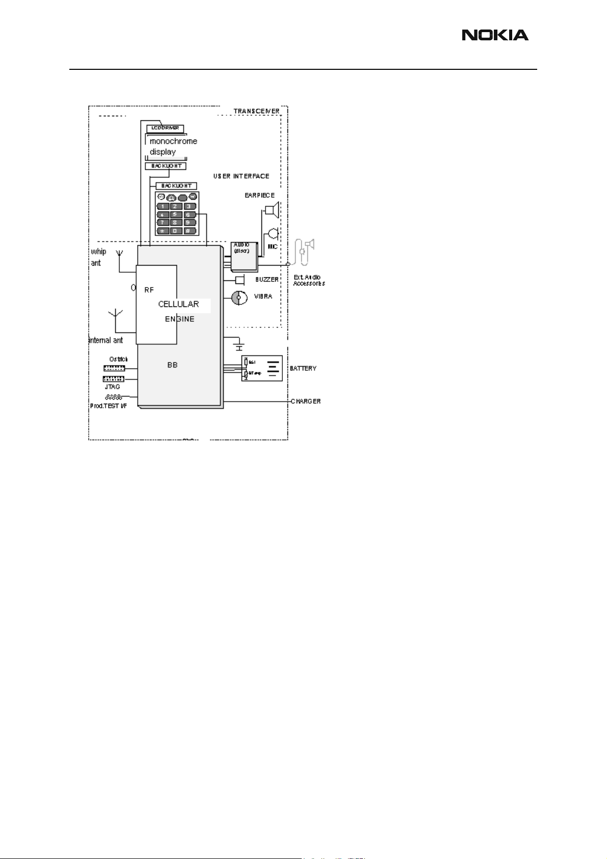
Transceiver RH-17
Introduction
The RH-17 is available as either CDMA 800 and AMPS or CDMA 800 only, depending on
model. It supports the new CDMA 1XRTT standard air interface.
Advanced messaging features include SMS (MO/MT), Instant Messaging, Nokia ‘Chat’
and Smart Messaging (ring tones, graphics, images, and animations).
The standard internal battery (BL-5C) provides users with up to 2:40 hours of talk time
(digital) and 1:45 hours of talk time (analog). Standby time is 280 hours (digital) and
25 hours (analog).
Two antennas are used — internal; external, extendable silver “whip”. When the whip
antenna is in, only the internal antenna is active. When the whip is retracted, both
antennas are active. Access to test the cellular engine is possible once the A cover is
removed.
Operational Modes
There are several different operational modes: Modes have different states controlled by
the cellular SW. Some examples are: Idle State (on ACCH), Camping (on DCCH), Scanning, Conversation, No Service Power Save (NSPS) previously OOR = Out of Range.
In the power-off mode, only the circuits needed for power-up are active.
In the idle mode, circuits are powered down and only the sleep clock is running.
In the active mode, all the circuits are supplied with power, although some parts might
be in idle state part of the time.
The charge mode is effective in parallel with all previous modes. The charge mode itself
consists of two different states; i.e., the fast charge and the maintenance mode.
The local and test modes are used for alignment and testing.
Issue 1 04/2003 Nokia Corporation Confidential Page 5
Page 6
RH-17
System Module CCS Technical Documentation
Figure 1: Interconnecting Diagram
Page 6 Nokia Corporation Confidential Issue 1 04/2003
Page 7

RH-17
CCS Technical Documentation System Module
Engine Module
Environmental Specifications
Normal and extreme voltages
Voltage range:
• nominal battery voltage: 3.6 V
• maximum battery voltage: 4.2 V
• minimum battery voltage: 3.2 V
Temperature Conditions
Temperature range:
• ambient temperature: -30...+ 60o C
• PWB temperature: -30...+85o C
Issue 1 04/2003 Nokia Corporation Confidential Page 7
Page 8
RH-17
System Module CCS Technical Documentation
Baseband Module
The core part of the RH-17 baseband module consists of three ASICs—UEM and UPP—
and flash memory. The following sections describe these parts.
UEM
UEM Introduction
UEM is the Universal Energy Management IC for DCT4 digital handportable phones. In
addition to energy management, it performs all the baseband mixed-signal functions.
Most of UEM pins have 2kV ESD protection. Those signals that are considered to be
exposed more easily to ESD have 8kV protection inside UEM. Such signals are all audio
signals, headset signals, BSI, Btemp, Fbus, and Mbus signals.
Regulators
UEM has six regulators for baseband power supplies and seven regulators for RF power
supplies. VR1 regulator has two outputs VR1a and VR1b.
Bypass capacitor (1uF) is required for each regulator output to ensure stability.
Reference voltages for regulators require external 1uF capacitors. Vref25RF is reference
voltage for VR2 regulator; Vref25BB is reference voltage for VANA, VFLASH1, VFLASH2,
VR1 regulators; Vref278 is reference voltage for VR3, VR4, VR5, VR6, VR7 regulators;
Page 8 Nokia Corporation Confidential Issue 1 04/2003
Page 9
RH-17
CCS Technical Documentation System Module
VrefRF01 is reference voltage for VIO, VCORE, VSIM regulators, and for RF.
BB RF
VANA: 2.78Vtyp 80mAmax VR1a:4.75V 12mAmax
VR1b:4.75V 12mAmax
Vflash1: 2.78Vtyp 70mAmax
Vflash2: 2.78Vtyp
40mAmax
VSim: 1.8/3.0V 25mAmax VR3:2.78V 20mA
VIO: 1.8Vtyp
150mAmax
Vcore: 1.0-1.8V
200mAmax
VR2:2.78V 100mAmax
VR4: 2.78V 50mAmax
VR5: 2.78V 50mAmax
VR6: 2.78V 50mAmax
VR7: 2.78V 45mAmax
VANA regulator supplies internal and external analog circuitry of BB. It's disabled in
sleep mode.
Vflash1 regulator supplies LCD and digital parts of UEM ASIC. It is enabled during startup
and goes to low Iq-mode in sleep mode.
Vflash2 regulator is not used on RH-17. It could be enabled/disenabled through writing
register and default is off.
VIO regulator supplies both external and internal logic circuitries. It's used by LCD, flash,
Robin, Batman, and UPP. Regulator goes in to low Iq-mode in sleep mode.
VCORE regulator supplies DSP and Core part of UPP. Voltage is programmable and the
startup default is 1.5V. Regulator goes to low Iq-mode in sleep mode.
VR1 regulator uses two LDOs and a charge pump. This regulator is used by Robin RF ASIC
(VR1B) and synthesizer circuits (VR1A).
VR2 is a linear regulator used to supply Robin RF ASIC and the detector circuitry.
VR3 is a linear regulator used by Robin RF ASIC and VCTCXO circuitry.
VR4 is a linear regulator used by the PLL and UHF VCO circuitry.
VR5 is a linear regulator used by the Batman RFIC and the Alfred RF ASIC.
VR6 is a linear regulator used by Robin RF ASIC and TX LO buffer.
VR7 is a linear regulator used by Batman RF ASIC.
Issue 1 04/2003 Nokia Corporation Confidential Page 9
Page 10

RH-17
System Module CCS Technical Documentation
IPA1 and IPA2 are programmable current generators. The 27k Ohm external resistor is
used to improve the accuracy of output current. IPA1 is used by lower band PA and IPA2
is used by higher band PA.
RF Interface
UEM handles the interface between the baseband and the RF section. It provides A/D and
D/A conversion of the in-phase and quadrature receive and transmit signal paths, and
also A/D and D/A conversions of received and transmitted audio signals to and from the
UI section. The UEM supplies the analog AFC signal to the RF section according to the
UPP DSP digital control. It also converts PA temperature into real data for the DSP.
Charging Control
The CHACON block of UEM asics controls charging. Needed functions for charging controls are pwm-controlled battery charging switch, charger-monitoring circuitry, battery
voltage monitoring circuitry and RTC supply circuitry for backup battery charging. In
addition, external components are needed for EMC protection of the charger input to the
baseband module. The DCT4 baseband is designed to electrically support both DCT3 and
DCT4 chargers.
Digital Interface
Data transmission between the UEM and the UPP is implemented using two serial connections, DBUS (9.6 MHz) for DSP and CBUS (1.2 MHz in CDMA) for MCU. UEM is a dualvoltage circuit: the digital parts are running from 1.8V and the analog parts are running
from 2.78V. Vbat (3,6V) voltage regulators inputs also are used.
Audio Codec
The baseband supports two external microphone inputs and one external earphone output. The inputs can be taken from an internal microphone, from a headset microphone,
or from an external microphone signal source through a headset connector. The output
for the internal earpiece is a dual-ended type output, and the differential output is capable of driving 4Vpp to the earpiece with a 60 dB minimum signal to total distortion ratio.
Input and output signal source selection and gain control is performed inside the UEM
ASIC according to control messages from the UPP. Both a buzzer and an external vibra
alert control signals are generated by the UEM with separate PWM outputs.
UI Drivers
There is a single output driver for buzzer, vibra, display, and keyboard LEDs inside UEM.
These generate PWM square wave to devices.
AD Converters
There is an 11-channel analog-to-digital converter in UEM. The AD converters are calibrated in the production line.
Page 10 Nokia Corporation Confidential Issue 1 04/2003
Page 11
RH-17
CCS Technical Documentation System Module
BB-RF Interface Connections
All the signal descriptions and properties in the following tables are valid only for active
signals.
Table 1: PDM Interface
Signal name From To Parameter Min Typ Max Unit Function
RX_IF_AGC UPP
GenIO 9
TX_IF_AGC UPP
GenIO 7
TX_RF_AGC UPP
GenIO 26
PA_GAIN UPP
GenIO 11
Signal
name
From To Parameter Input characteristics Function
Batman Voltage Min
Max
---------------Clk Rate
Robin Vo ltage Min
Max
---------------Clk Rate
Robin Vo ltage Min
Max
---------------Clk Rate
Robin Vo ltage Min
Max
---------------Clk Rate
(1)
0.0
1.75
--------
(1)
0.0
1.75
-------
0.0
1.75
--------
(3)
0.0
1.75
--------
(3)
Table 2: General I/O Interface
1.8
------
9.6
1.8
-------
9.6
1.8
--------
9.6
1.8
--------
9.6
0.1
1.86
-------
19.2
0.1
1.86
--------
19.2
0.1
1.86
--------
19.2
0.1
1.86
--------
19.2
V
-------MHz
V
-------MHz
V
-------MHz
V
-------MHz
Controls gain of VGA r
in receiver
Controls gain of VGA
in IF VGA in Robin
Controls gain of TX
driver in Robin
Controls gain of PA
TX_Gate UPP
Gen IO 8
pullup
PA_Boost UPP
Gen IO 03
pullup
FAST_AGC UPP
Gen IO 13
pullup
SYNTH_LE UPP
Gen IO 25
pullup
Robin “1” Transmitter Off
“0” Transmitter On
Timing Accuracy
Snapper
Shark
Robin “1” AMPS mode
Synthesizer
“1” boost mode
“0” data mode
Timing Accuracy
“0” CDMA mode
“1” Enable
“0” Disable
1.38 1.88 V
0 0.4 V
4 chips, and can be up
to a total of 255 chips
1.38 1.88 V
0 0.4 V
4 chips, and can be up
to a total of 255 chips
1.38 1.88 V
0 0.4 V
4 chips, and can be up
to a total of 255 chips
1.38 1.88 V
0 0.4 V
4 chips, and can be up
to a total of 255 chips
Punctures the PA’s and
the Robin ASIC
Digital Into RF
Sets PA current for
desired linearity
Digital Into RF
Sets phone mode of
operation AMPS or
CDMA
Digital into RF
Latch enable for synthesizer
Digital into RF
Issue 1 04/2003 Nokia Corporation Confidential Page 11
Page 12

RH-17
System Module CCS Technical Documentation
Table 3: VCTCXO Interface
Signal name From To Parameter Min Typ Max Unit Function
CLK192M_UPP VCTCXO Upp
Batman
Robin
UHF PLL
AFC UEM VCTCXO Voltage Min
Frequency
-----------------------Signal amplitude
Max
------------------------Settling time
Table 4: Regulated Supplies from UEM to RF
Signal
name
VBAT Battery PA & UEM,
VR1A UEM UHF Synth Voltage
From To Parameter Min Typ Max Unit Function
Voltage
external driver
amps
----------------
Current
----------------
Current
(4)
-------
0.5
0.0
2.4
------- -------
3.2
----0
4.6
-----0
3.5
------
4.75
-----4
19.2
-------
1.0
-------
1.5
0.1
2.55
-------
0.2
5.1
-----2A
peak
4.9
-----5
MHz
-------
Vpp
V
------ms
V
------
V
-----mA
High stability clock
signal for logic circuits, AC coupled
sinewave.
Analog Out of RF
Automatic frequency control
signal for VCTCXO
Digital Into RF
Battery supply.
Lower limit is to
guarantee regulator PSRR
Charge pump + linear regulator.
VR1B UEM PA Iref current
sources in
Robin
VR2 UEM Robin driver
amps
VR3 UEM VCTCXO Robin
VHF synthesizer
VR4 UEM UHF VCO, syn-
thesizer
VR5 UEM Batman IF, BB,
LNA, mixer
VR6 UEM Robin IF, BB,
mixers
VR7 UEM Batman VHF
synthesizer
VREFRF01 UEM Batman Vref Voltage 1.334 1.35 1.366 V Voltage Reference
Voltage
----------------
Current
Voltage
----------------
Current
Voltage
----------------
Current
Voltage
----------------
Current
Voltage
----------------
Current
Voltage
----------------
Current
Voltage
----------------
Current
4.6
-----0
2.70
------
2.70
------
2.70
------
2.70
------
2.70
------
2.70
------
4.75
-----4
2.78
------
2.78
------
2.78
------
2.78
------
2.78
------
2.78
------
4.9
-----5
2.86
-----100
2.8
-----20
V
-----mA
V
-----mA
V
-----mA
V
-----mA
V
-----mA
V
-----mA
V
-----mA
Charge pump + linear regulator
Linear regulator
Low noise linear
regulator for
VCTCXO
Low lq linear regulator
Low lq linear regulator
Low lq linear regulator
Low noise linear
regulator for synthesizer
for RF-IC 1.2%
accuracy
Page 12 Nokia Corporation Confidential Issue 1 04/2003
Page 13

RH-17
CCS Technical Documentation System Module
Table 4: Regulated Supplies from UEM to RF
Signal
name
VREFRF02 UEM Robin Vref Vol tage 1.334 1.35 1.366 V Voltage Reference
VIO UEM Digital IO + PLL
From To Parameter Min Typ Max Unit Function
for RF-IC 1.2%
accuracy
digital
Voltage
----------------
Current
1.70
------
1.8 1.88
-----50
V
-----mA
Supply for RF-BB
digital interface
and some digital
parts of RF.
Table 5: Slow A/D Converters
Signal name From To Parameter Min Typ Max Unit Function
PA_TEMP Thermistor UEM Input voltage
range
---------------Input clock freq
PWROUT Robin UEM Input voltage
range
---------------Input clock freq
0
------- ------
0
------- ------
2.741
--------
2.5
2.741
--------
2.5
V
-----MHz
V
-----MHz
PA temperature sensor output voltage
Analog Out of RF
Buffered output of TX
output detector and
TX power supply
Analog Out of RF
FALSE_DET Robin UEM Input voltage
range
---------------Input clock freq
0
------- ------
2.741
--------
2.5
V
-----MHz
protection circuit
that is independent
of main transmitter
on-off control circuit
and minimizes the
possibility of false
transmission caused
by component failure
Table 6: RF-BB Analog Signals
Signal name From To Parameter Min Typ Max Unit Function
RX_IP_RF
RX_IN_RF
RX_QP_RF
RX_QN_RF
TX_IP_RF
TX_IN_RF
TX_QP_RF
TX_QN_RF
Batman UEM Differential volt-
age swing (static)
-------------------------DC level
-------------------------Input Bandwidth
UEM Robin Differential volt-
age swing (static)
--------------------------DC level
---------------------------
-3 dB Bandwidth
1.35
--------
1.3
--------
--------
1.65
-------650
1.4
-------
1.35
-------
0.9
-------
1.7
-------
1.45
--------
1.4
-------615
1.0
-------
1.75
-------1950
Vpp
------V
------kHz
Vpp
------V
------kHz
Differential in-phase
and quadrature RX
baseband signal
Analog Out of RF
Differential quadra-
ture phase TX baseband signal for RF
modulator
Analog into RF
Issue 1 04/2003 Nokia Corporation Confidential Page 13
Page 14

RH-17
System Module CCS Technical Documentation
Table 7: RFIC Control
Signal name From To Parameter Min Typ Max Unit Function
RF_BUS_CLK
RF_BUS_DATA
RF_BUS_EN1X
SYNTH_LE UPP PLL Voltage
UPP Robin/Batman/
PLL
High-level input
voltage, V
Low-level input
voltage, V
High-level output
voltage, V
Low-level output
voltage, V
Clock
Timing reso lu t i on
Table 8: RFIC Control
Signal
name
PURX UEM Robin/Batman Voltage Level
From To Parameter Min Typ Max Unit Function
------------------------Timing resolution
IH
IL
OH
OL
0
-------- -------
1.8
-------10
2.35
0.5
2.45
0.4
10
V
-----us
V
V
V
V
MHz
V
us
Power Up Reset
for Batman and
Robin
1.2
1.3
01.8
1.3
1.4
9.72
Serial Clock =
Digital Into RF
Bidirectional
Serial Date =
Digital I/O
Latch enable
for Batman and
Robin = Digital
Into RF
Synthesizer
latch enable
UPP
UPP Introduction
RH-17 uses UPP8Mv2.2 ASIC. The RAM size is 8Mbit. The UPP ASIC is designed to operate in a DCT4 engine, and is designed as part of the DCT4 common baseband task force.
The DCT4 processor architecture consists of both DSP and MCU processors.
Blocks
UPP is internally partitioned into two main parts: the Brain and the Body.
The Brain consists of the Processor and Memory System (i.e., Processor cores, Mega-cells,
internal memories, peripherals and external memory interface). The following blocks are
included: the DSP Subsystem (DSPSS), the MCU Subsystem (MCUSS), the emulation control EMUCtl, the program/data RAM PDRAM, and the Brain Peripherals–subsystem
(BrainPer).
The Body consists of the NMP custom cellular logic functions. These contain all interfaces and functions needed for interfacing with other DCT4 baseband and RF parts. It
includes the following sub-blocks: MFI, SCU, CTSI, RxModem, AccIF, UIF, Coder, GPRSCip,
BodyIF, SIMIF, PUP and CDMA (Corona).
Page 14 Nokia Corporation Confidential Issue 1 04/2003
Page 15

RH-17
CCS Technical Documentation System Module
Flash Memory
Introduction
Flash memory is a high-performance, 64-Mbit, single power supply 1.8 Volt-only FLASH
memory device. This device is designed to be programmed in-system with the standard
system 1.8-volt Vcc supply. A 12.0 volt Vpp is not required for program or erase operations, although an acceleration pin is available if faster write performance is required.
The device is a boot-sectored device, consisting of eight 8Kb and 63 sectors of 64Kb
each.
The device has two read modes: asynchronous read and burst mode read. Device powersup in an asynchronous read mode. In the asynchronous mode, the device has two control
functions which must be satisfied in order to obtain data at the outputs. In the linear
mode, the device will deliver a continuous sequential word stream starting at the specified word and continuing until the end of the memory or until the user loads in a new
starting address or stops the burst advance. The burst mode read operation is a synchronous operation tied to the rising edge of the clock. The microprocessor supplies only the
initial address; all subsequent addresses are automatically generated by the device at the
rising edge of subsequent clock cycles. The burst read cycle consists of an address phase
and a corresponding data phase. The device also is capable of Burst Suspend and Burst
Resume operations.
In order to reduce the power consumption on the bus, a Power Save function is introduced. This reduces the amount of switching on the external bus.
User Interface Hardware
LCD
Introduction
RH-17 uses a 96x65 monochrome display. Dimensions for the display are 38.4 mm x 37.6
mm x 1.6 mm, with an active area of 31.15 mm x 24.78 mm.
Interface
LCD is controlled by UI SW and control signals.
Booster capacitor (C302 1uF) is connected between booster pin (Vout) and ground. The
capacitor stores boosting voltage.
Keyboard
Introduction
RH-17 keyboard design is Nokia Jack style, with up and down navigation keys, two soft
keys, 12 number keys. The PWR key is located on top.
Power Key
All signals for keyboard are coming from UPP asic except pwr key signal which is con-
Issue 1 04/2003 Nokia Corporation Confidential Page 15
Page 16

RH-17
System Module CCS Technical Documentation
nected directly to UEM. Pressing of pwr key is detected so that switch of pwr key connects PWONX is of UEM to GND and creates an interrupt.
Keys
Other keys are detected so that when a key is pressed down, the metal dome connects
one S-line and one R-line of UPP to GND and creates an interrupt for SW. Matrix of how
lines are connected and which lines are used for different keys is described in the following table. S-line S0 and R-line R5 are not used.
NC = Not Connected
Lights
Introduction
RH-17 has seven white LEDs for lighting purposes: four (V300, V301, V302, V303) are for
keyboard (typeLWL88S) and three (V304, V305, V306) are for display (type LWY87). LED
type is white-light emitting diode.
Interfaces
Returns /
Scans
R0 NC Send End NC
R1 Soft left Up Down Soft right
R2 1 4 7 *
R3 2 5 8 0
R4 3 6 9 #
S1 S2 S3 S4
Display keyboard lights are controlled by UEM Klight signal (8-bit register DriverPWMR,
bits 7...4). Klight output is turned ON, which controls the LED driver (LM2795B) used to
control the current going through the LEDs. A constant current source is used to ensure
that the LEDs provide uniform intensity and color.
Technical Information
LEDs have white plastic body around the diode itself, which directs the emitted light to
UI side. Current for keypad lights is limitied by resistor between Vbatt and LEDs.
Vibra
Introduction
Vibra is located on the D-cover and is connected by spring connectors on the PWB. It is
located in the left bottom side of the engine.
Interfaces
Vibra is controlled by pwm signal VIBRA from UEM. This signal allows control of both
Page 16 Nokia Corporation Confidential Issue 1 04/2003
Page 17

RH-17
CCS Technical Documentation System Module
frequency and pulse width of signal. Pulse width is used to control current when battery
voltage changes. Frequency control searches for optimum frequency to ensure silent and
efficient vibrating.
Parameter Requirement Unit
Rated DC Voltage 1.3 V
Rated speed 9500 ±3000 rpm
Rated current 11 5 ±20 mA
Starting current 150 ±20 mA
Armature resistance 8.6 ohm
Rated DC voltage available 1.2 to 1.7 V
Starting DC voltage min. 1.2 V
Audio Hardware
Earpiece
Introduction
The 13 mm speaker capsule that is used in DCT3 products also is used in RH-17.
The speaker is dynamical—very sensitive, and capable of producing relatively high sound
pressure at low frequencies. The speaker capsule and surrounding mechanics comprise
the earpiece.
Microphone
Introduction
The microphone is an electric microphone with omnidirectional polar pattern. It consists
of an electrically polarized membrane and a metal electrode, which form a capacitor. Air
pressure changes (i.e., sound) move the membrane, which causes voltage changes across
the capacitor. Since the capacitance is typically 2 pF, a FET buffer is needed inside the
microphone capsule for the signal generated by the capacitor. The microphone needs
bias voltage as a result of the FET.
Battery
Phone Battery
Introduction
An 850 mAh Li-ion battery (BL-5C) is standard in RH-17.
Interface
The battery block contains NTC on phone and BSI resistors for temperature measurement
Issue 1 04/2003 Nokia Corporation Confidential Page 17
Page 18

RH-17
System Module CCS Technical Documentation
and battery identification. The BSI fixed resistor value indicates the chemistry and
default capacity of a battery. NTC resistor measures the battery temperature. Temperature and capacity information is needed for charge control. These resistors are connected
to the BSI battery connector and the NTC is connected to BTEMP pins of UEM. Phone has
pull-ups on these lines so that they can be read by A/D inputs in the phone (see the following figure). Resistors on phone are ESD protection. There also are spark caps in the
BSI line to prevent ESD.
Batteries have a specific red line to indicate if the battery has been subjected to excess
humidity. The batteries are delivered in a "protection" mode, which gives longer storage
time. The voltage seen in the outer terminals is zero (or floating), and the battery is activated by connecting the charger. Battery has internal protection for overvoltage and
overcurrent.
Battery Connector
RH-17 uses a spring-type battery connector. This makes the phone easier to assemble in
production and ensures a more reliable connection between the battery and PWB.
Signal
#
name
Figure 2: Connector order for Lynx batteries
Connected
from - to
Batt. I/O
Signal properties
A/D--levels--freq./timing
Description /
Notes
1 VBAT (+) (batt.) VBAT I/O Vbat
2 BSI BSI (batt.) UEM Out Ana.
3 GND GND GND Gnd
Page 18 Nokia Corporation Confidential Issue 1 04/2003
Page 19

RH-17
CCS Technical Documentation System Module
Accessories Interface
System connector
Introduction
RH-17 uses the Tomahawk accessories via the Tomahawk connector.
Interface
Tomahawk bottom connector consists of charging plug socket and Tomahawk System
connector (see figures that follow). Minimum configuration of Tomahawk interface
includes charging, mono audio, power out, ACI and Fbus. USB and stereo audio out are
optional.
Tomahawk system connector includes:
•Charging
Pads for 2 -wire charging in cradles
• Audio (Stereo audio optional)
FM radio antenna connection (may be option with accessory)
2-wire differential mic input
• Power out
2.78V 70 mA output to accessories (bb4.0, bb4.5)
2.5V 90 mA output to accessories (bb5.0)
• Detection/controlling
ACI
Point to point bi-directional data line
• USB (Optional)
Power in 5V in from USB host
USB v2.0 device mode ( Full speed 12M )
•Fbus
Standard Fbus
Issue 1 04/2003 Nokia Corporation Confidential Page 19
Page 20

RH-17
XMIC P
2.70
HSEAR P HSEAR N
System Module CCS Technical Documentation
AT command mode (Nokia Serial Bus)
Phonet message mode
Fast Fbus, fast data bus to add on modules
Figure 3: Tomahawk system connector
6.50
9.50
6.55
5.40
1.00
21.20
PWB
5.70
0.30
Metal
shielding
ACI
Vout
Charge GND
Shielding GN D
USB Vbus
USB D+ / Fbus RX
USB D- / Fbus TX
XMIC N
DATA GND
HSEAR R P
HSEAR R N
Shielding GND
3.50
Figure 4: Mechanical dimensions and signals of Tomahawk bottom connectors
Page 20 Nokia Corporation Confidential Issue 1 04/2003
Page 21

RH-17
CCS Technical Documentation System Module
An accessory is detected by the ACI-line. All accessories will generate interrupt while
inserted or removed from the phones Tomahawk system connector. Insertion of an accessory will generate HEADINT interrupt by pulling ACI line down. Vout is enabled by UPP.
The MBUS line is connected to HEADINT line. If HEADINT interrupt from low to high
transition occurs within 20msec a more advanced accessory is connected else a basic
headset is connected. The accessory flowchart outlines the routines used for all accessory detection.
The following diagram illustrates accessory detection / external audio flowchart.
Issue 1 04/2003 Nokia Corporation Confidential Page 21
Page 22

RH-17
System Module CCS Technical Documentation
Accessory
detection
Headint from hi to low tran
Power Vout line
Enable Vbus if USB not in use
Connect MBUS to Headint line
= 4.7k pullup to headint line
Low to high tran in
Headint line in 20ms
NO
Headint YES
ACI or Fbus
accessory connected
Start ACI detection
USB
detection
High to low tran in Vp
and Vm - lines
Connect 1.3k resistor to D+ line
Host with detect phone as
full speed device
USB host
detected
Disconnect MBUS
from headint
Disable FBUS
Unpower VOUT line
Basic
headset
detected
NO
3.th trial ?
YES
Nokia Serial Bus
accessory detected
(AT mode)
Send ACI reset pulse
Phone gets learning
sequence from ACI
ASIC
Enable FBUS HW and
set FBUS to
requested command
mode, default is AT
command mode
Wait accessory ID
from Fbus Rx line
Fbus accessory
detected (phone
mode)
YESNO
YES
Read acc features
from ACI ASIC
FBUS needed?
NO
ACI accessory
detected
Figure 5: Accessories Detection Flowchart
Page 22 Nokia Corporation Confidential Issue 1 04/2003
Page 23

RH-17
CCS Technical Documentation System Module
TTY/TTD and Universal Headset Jack
TTY/TTD devices use standard 2.5 mm 3-pin plug (tip = transmit, ring = receive, sleeve =
ground) while universal headset also uses same type of plug (tip = microphone, ring =
earpiece, sleeve = ground). Since only three pins are available for both transmit and
receive at same time, both paths have to use single-end design (share the ground). The
detection scheme for this interface uses a built-in normally closed switch in the universal headset jack. When there is no device being plugged in, the switch is closed which
forces the level on the detection line (GENIO(12)) to 1.8V. When a device is plugged in,
the voltage is set to 0V. The detection line then can identify whether a device is plugged
in or not.
Charger IF
Introduction
The charger connection is implemented through the bottom connector. DCT-4 bottom
connector supports charging with both plug chargers and desktop stand chargers.
There are three signals for charging. Charger gnd pin is used for both desktop and for
plug chargers as well as charger voltage. PWM control line, which is needed for 3-wire
chargers, is connected directly to gnd in module PWB so the RH-17 engine doesn't provide any PWM control to chargers. Charging controlling is done inside UEM by switching
UEM internal charger switch on/off.
Interface
The fuse F100 protects from high currents (e.g., when broken or pirate chargers are used).
L100 protects engine from RF noises, which may occur in charging cable. V100 protects
UEM ASIC from reverse polarity charging and from high charging voltage. C106 is also
used for ESD and EMC protection.
Issue 1 04/2003 Nokia Corporation Confidential Page 23
Page 24

RH-17
X
System Module CCS Technical Documentation
Test Interfaces
Production Test Pattern
Interface for RH-17 production testing is 5-pin pad layout in BB area (see figure below).
Production tester connects to these pads by using spring connectors. Interface includes
MBUS, USRX, FBUSTX, VPP, and GND signals. Pad size is 1.7mm. The same pads also are
used for AS test equipment such as module jig and service cable.
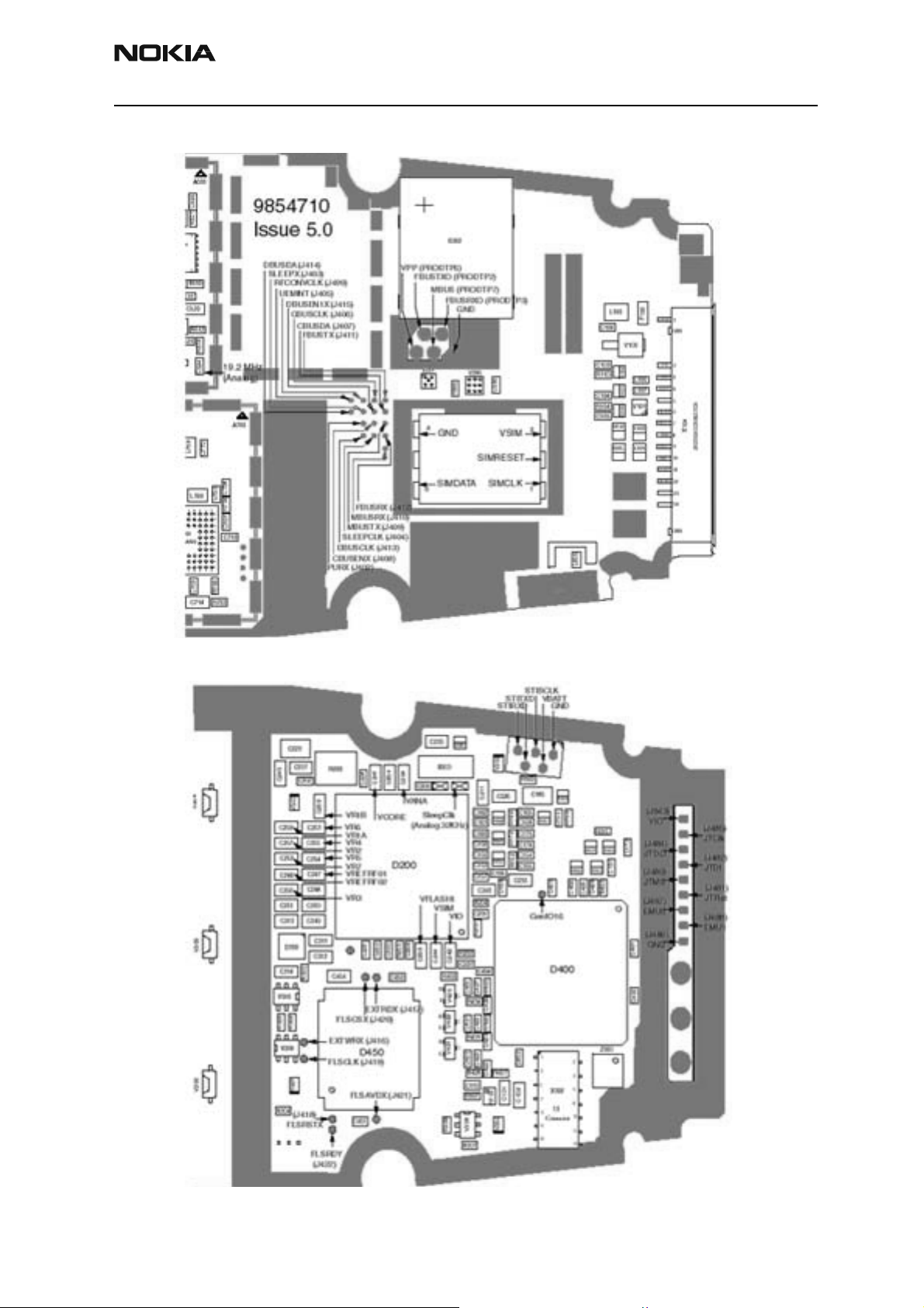
Other Test Points
BB ASICs and flash memory are chip scale package (CSP) components and the visibility
is very poor. This makes measuring of most of the BB signals impossible. In order to
debug BB at least at some level, the most important signals can be accessed from test
points. The figures below show test points throughout the PWB for all cricital signals.
DBUSCLKDBUSDA
2.
FBUS_TX
6.
VPP
SLEEPCLK
3.
FBUS_R X
8.
7.
MBUS
UEM (D200)
CBUSDA
GND
CBUSENX
CBUSCLK
FBUSTX
J414
J403
J413
J402
PURXSLEEPX
J404
J407
J405
UEMINT
UPP (D400)
J408
J415
DBUSEN1X
J406
J412
FBUSRX
J411
J409
MBUSTX MBUSR
J410
Page 24 Nokia Corporation Confidential Issue 1 04/2003
Page 25
RH-17
CCS Technical Documentation System Module
Issue 1 04/2003 Nokia Corporation Confidential Page 25
Page 26

RH-17
System Module CCS Technical Documentation
EMC
General
EMC performance of the RH-17 baseband is improved by using ESD components: V101,
L103, L104, R105, R112, R113, Z300, and spargaps to protect UEM, UPP, and Flash. UEM
has internal protection against +/-8kV ESD pulse.
BB Component and Control I/O Line Protection
Keyboard Lines
ESD protection for the keyboard is provided by component Z300. The device is designed
to reduce EMI and RFI noise. In addition, this integrated device includes ESD protection
circuitry that will protect the phone’s ASICs from destruction when subjected to ESD
surges up to 15kV.
PWB
All edges are grounded from both sides of PWB and solder mask is opened from these
areas. Target is that any ESD pulse faces ground area when entering the phone (e.g.,
between mechanics covers).
LCD
ESD protection for LCD is implemented by connecting metal frame of LCD to gnd. Connection is only on one side, at the top of the LCD, and that is not the best solution. Due
to SAR issues, the C-cover metallization is cut in the middle, just under the display, making the whole engine more sensitive to ESD. Software protects against LCD crashing.
Microphone
Microphone is an unsymmetrical circuit, which makes it well protected against EMC.
EARP
EARP is protected with the R170 dual package varistor.
Bottom Connector Lines
XMICP, XMICN, XEARP, XEARN lines have varistors R105 and R112, as well as the EMI filters L103 and L104.
Hookint has same protection as XMICP and HeadInt has RC-circuit protection.
Charger + is protected with a ferrite bead (42W/100MHz) and capacitor to ground (1n).
Charger - is connected to GND.
Battery Connector Lines
BSI is protected with spark gaps and RC circuit (47k & 10n) where resistors are size 0603.
Page 26 Nokia Corporation Confidential Issue 1 04/2003
Page 27

RH-17
CCS Tech nical Documentation System Module
M-bus F-bus
ESD protection for M-bus and F-bus is done with spargaps and an ESD ASIC (V201).
General Information About Testing
Phone operating modes
Phone has three different modes for testing/repairing phone. Modes can be selected with
suitable resistors connected to BSI- and BTEMP- lines as follows:
Mode BSI- resistor BTEMP- resistor Remarks
Normal 68k 47k
Local 3.3K ohms 47k ohms
Test 6.8k ohms 47k ohms Recommended with base-
band testing. Same as
local mode, but making a
phone call is possible.
The MCU software enters automatically to local or test mode at start-up if corresponding resistors are connected.
Note! Baseband doesn't wake up automatically when the battery voltage is connected (normal mode).
Power can be switched on by
• pressing the PWR key
• connectin g a charger
• RC-alarm function
In the local and test mode, the baseband can be controlled through MBUS or FBUS (FBUS
is recommended) connections by Phoenix service software.
RF Module
Requirements
The RH-17 RF module supports CDMA800 as described in:
• IS2000-2-A Physical Layer Standard for cdma2000 Spread Spectrum Systems; and
• IS-98D (Draft 4) Recommended Minimum Performance Standard for Spread Spectrum
Mobile Stations.
Temperature Conditions
Surface temperature (SPR5 - Product Safety)
Issue 1 04/2003 Nokia Corporation Confidential Page 27
Page 28

RH-17
System Module CCS Te chnical Documentation
Maximum temperature rise is 50o C for nonmetallic surfaces and 30o C for metal surfaces at room temperature.
Other temperature requirements (SPR4 - Operating Conditions)
o
Meeting requirements: -30...+ 60
Storage requirements: -30...+85o C
C
Main Technical Characteristics
Environmental Specifications
Normal and extreme voltages
Voltage range:
• nominal battery voltage: 3.6 V
• maximum battery voltage: 4.2 V
• minimum battery voltage: 3.2 V
Temperature conditions:
• ambient temperature: -30...+ 60o C
• PWB temperature: -30...+85o C
• storage temperature range: -40 to +85o C
Antenna
A single-band, whip antenna/internal antenna combination is used.
Page 28 Nokia Corporation Confidential Issue 1 04/2003
Page 29

RH-17
CCS Tech nical Documentation System Module
Transmitter
Figure 6: Trimode block diagram
The transmit chain up to the RF driver stage is integrated into one transmit-integrated
circuit called Robin, with external power amplifiers (PA). The channel spacing is 50 kHz.
All data transmitted on the channel is convolutionally encoded and block-interleaved.
Modulation is 64-ary orthogonal (RC1 and RC2) and direct sequence spread by a quadrature pair of PN sequences at a fixed chip rate. The data is filtered, O-QPSK modulated
and up-converted to the appropriate transmission frequency. RC3 and RC4 use HPSK
modulation at data rates up to 153.6 kBPS (RC3) and 115.2 kBPS (RC4).
The baseband I/Q signals are converted to IF frequency in the I/Q modulator by Quadrature mixing. The modulated IF signals go through a variable gain amplifier (IF AGC) and
then are routed to the TX path. The path consists of an upconverter and a variable gain
RF amplifier. The IF signal is converted up to RF with a differential output upconverter
and then fed to the RF amplifier. The RF amplifier has variable gain capability (RF AGC)
with up to 40 dB of dynamic gain control.
The outputs of the RF amplifiers are differential. The differential outputs from Robin are
combined into single-ended output by an external balun and fed into an external driver
amplifier module (Tomcat).
The output of the Tx saw filter is connected to the PA. Out of the PA is an isolator, then
the antenna.
The PA modules contain all the necessary matching networks and reference current circuitry for variable gain control and biasing ON/OFF. A variable reference current is used
to vary the PA gain and PA bias current. The variable gain technique reduces PA current
consumption and improves the signal-to-noise ratio at low output power levels. The precision bias current (and gain) control is achieved by varying the PA reference current
Issue 1 04/2003 Nokia Corporation Confidential Page 29
Page 30

RH-17
System Module CCS Te chnical Documentation
with a PDM control voltage.
The transmitter chain utilizes smart power techniques and only the required circuits are
powered at the appropriate times. In order to save energy in puncture mode, when there
is no speech activity during a call, the driver and power amplifiers and the Robin IC are
switched ON and OFF rapidly. These units also are in the OFF state when the transmitter
is in standby. The ON/OFF switch commands are issued by a Digital ASIC (UPP). The UPP’s
PDM controls a current mirror in Robin that provides the PA reference current. Switching
each reference current ON/OFF switches each PA ON/OFF. The VHF synthesizer and power
detector circuits are left on during the puncture mode.
Synthesizer
Refer to Figure 6 for a block diagram that illustrates all three synthesizers and how they
interconnect in the system.
Page 30 Nokia Corporation Confidential Issue 1 04/2003
Page 31

RH-17
CCS Tech nical Documentation System Module
Figure 7: Synthesizer System Block Diagram
UHF LO Synthesizer
The UHF LO synthesizer generates the first RX LO frequency for the receiver (down-conversion) and the second TX LO frequency for the transmitter (up-conversion). The synthesizer is a dual-modulus prescaler type and utilizes a phase-frequency detector with a
charge pump that sinks or sources currents, depending upon the phase difference
between the phase detector input signals.
For the cellular AMPS/CDMA band, channel spacing is 30 kHz. An external buffer is provided for high isolation between Robin and the VCO to reduce VCO pulling due to chang-
Issue 1 04/2003 Nokia Corporation Confidential Page 31
Page 32

RH-17
System Module CCS Te chnical Documentation
ing load.
1st TX VHF LO Synthesizer (Robin)
The TX VHF Synthesizer is integrated within the Robin RFIC and generates the LO signals
for the IQ-modulator in Robin. The synthesizer has an internal VCO with an external resonator. The VCO operates at two times the CELL IF frequencies. A band-switch signal,
VCO_Band, is used to shift the center frequency of the external resonator.
The synthesizer is a dual-modulus prescaler type, and utilizes a phase detector with a
charge pump that sinks or sources currents, depending on the phase difference between
the detector input signals. The width of the pulses depends on the phase difference
between the signals at input of the phase detector. The main divider, auxiliary divider,
and reference divider are programmable through the serial interface to Robin.
The TX VHF Synthesizer generates 346.2 MHz for Cell Band.
The TX VHF Synthesizer comparison frequency for Cell Band is 30 kHz.
2nd RX VHF LO Synthesizer (Batman)
The RX VHF Synthesizer is integrated within the Batman RFIC and generates the LO signals for the IQ demodulator in Batman. The synthesizer has an internal VCO with an
external resonator. The VCO operates at two times the common 128.1 MHz RX IF frequency. A band-switch signal, Band_Sel, is used to select the band of operation for the
UHF VCO.
The synthesizer is a dual-modulus prescaler type, and utilizes a phase detector with a
charge pump that signals or sources currents, depending upon the phase difference
between the detector input signals. The width of the pulses depends on the phase difference between the signals at input of the phase detector. The main divider, auxiliary
divider, and reference divider are programmable through the serial interface to Batman.
The RX VHF Synthesizer generates 256.2 MHz for Cell Band.
The RX VHF Synthesizer comparison frequency for Cell Band is 150 kHz.
VCTCXO - System Reference Oscillator
The VCTCXO provides the frequency reference for all the synthesizers. It is a voltage-controlled, temperature-compensated, 19.2MHz crystal oscillator that can be pulled over a
small range of its output frequency. This allows for an AFC function to be implemented
for any frequency accuracy requirements. This is done by DSP processing of received I/Q
signals.
Closed loop AFC operation allows very close frequency tracking of the base station to be
done in CDMA mode. This will enable the unit to track out aging effects and give the
required center frequency accuracy in cellular bands.
The most practical way of clock distribution is driving all three chips (UHF PLL, Batman,
and Robin) directly from the VCTCXO. A buffer is used to drive the UPP in order to isolate
Page 32 Nokia Corporation Confidential Issue 1 04/2003
Page 33

RH-17
CCS Tech nical Documentation System Module
the UPP’s digital noise from the VCTCXO, which prevents contamination of the 19.2 MHz
reference onto the PLL chips of the system. Since the VCTCXO output is a sinewave, such
clock distribution will not cause any clock signal integrity problems, even for relatively
long traces (what might occur in case of a digital square waveform with fast transition
times). The VCTCXO output is AC, coupled to Batman, Robin, UFH PLL, and the digital
ASICs (see figure) to eliminate DC incompatibility between those pins.
Receiver
The receiver is a dual conversion I/Q receiver with a first IF of 128.1 MHz. The front-end
RFIC (Alfred) contains a low noise amplifier (LNA), a radio frequency amplifier (RFA), a
down-converter, an intermediate frequency amplifier (IFA), and a local oscillator amplifier (LOA). Between the LNA and the RFA is a bandpass filter which will reject out-of-
Figure 8: VCTCXO Clock Distribution
Figure 9: RH-17 Receiver Block Diagram
Issue 1 04/2003 Nokia Corporation Confidential Page 33
Page 34

RH-17
System Module CCS Te chnical Documentation
band spurious and act as image rejection. The IF filter is between the Alfred IC and the
BatmanD IC. The purpose of this filter is to guarantee rejection in adjacent and alternate
channels.
The RX IF ASIC BatmanD is used to convert the IF down to baseband I and Q. The ASIC
contains a VGA section, IQ demodulator, baseband filters (BBFIL) for AMPS and CDMA.
Switchable gain baseband amplifier (BBAMP), and RX VHF PLL. The I/Q BB signals are
output to UEM chip for analog-to-digital conversion and further signal processing.
GE / CE Interface
The GE / CE interface has various control signals, a reference clock, a sleep clock, and
serial bus. There also are V
and VIO voltage generated in the CE baseband used to
CORE
power some of the GE.
Digital Supply Vio
This supply is used to power the GPS RF/BB interface lines and also to preserve configuration settings in the RFIC when it is in power-down mode. It originates from the CE
energy management system.
Parameter Units Min Typ Max
On Level V 1.65 1.8 1.95
Load Current - Active mA 1.6 3
Load Current – Sleep µA 240 350
Digital Supply Vcore
This supply is used to power the internal GPS Baseband ASIC during operation and to
preserve the internal state when it is in deep sleep mode. It originates from the CE
energy management system.
Parameter Units Min Typ Max
On Level V 1.425 1.5 1.65
Load Current - Active mA 26 35
Load Current – Sleep µA 30 500
Digital GE/CE Interface Signal Parameters
Parameter Units Min Typ Max
Hi Level Volts 0.8*Vio
Lo Level Volts 0.22*Vio
Page 34 Nokia Corporation Confidential Issue 1 04/2003
Page 35

RH-17
CCS Tech nical Documentation System Module
RF ASIC and LNA Supply V
The VRF supply is the main source of power for the RF IC. It originates in GPS baseband
section and will be turned off for power-saving sleep modes.
Parameter Units Min Typ Max
On Level V 2.7 2.8 3.3
Load Current - Active mA 40 55
RF
Issue 1 04/2003 Nokia Corporation Confidential Page 35
Page 36

RH-17
System Module CCS Te chnical Documentation
Page 36 Nokia Corporation Confidential Issue 1 04/2003
 Loading...