

Page 1

CCS Technical Documentation
RH-17 Series Transceivers
Troubleshooting — RF
Issue 1 04/2003 Confidential Nokia Corporation
Page 2

RH-17
Troubleshooting — RF CCS Technical Documentation
Page 2 Nokia Corporation Confidential Issue 1 04/2003
Page 3

RH-17
CCS Technical Documentation Troubleshooting — RF
Contents
Page No
RF Troubleshooting ....................................................................................................... 5
Test Steps .....................................................................................................................5
Troubleshooting Summary ..........................................................................................9
Tuning Description ....................................................................................................13
Test 1 TS Initial Current.......................................................................................... 13
Test 2 BB Flash Phone............................................................................................ 14
Test 5 ST DBUS...................................................................................................... 15
Test 6 ST CBUS...................................................................................................... 15
Test 7 ST Aux DA................................................................................................... 16
Test 8 ST EAR Data................................................................................................ 16
Test 9 ST SleeepX................................................................................................... 17
Test 10 ST TX / DP................................................................................................. 17
Test 11 ST TX Q DP............................................................................................... 18
Test 12 ST MIF Loopback...................................................................................... 18
Test 13 ST Sleep Clock........................................................................................... 19
Test 14 ST Batman VHFPLL.................................................................................. 19
Test 15 ST Robin VHF PLL CELL ........................................................................ 20
Test 16 ST TX Detector CELL ............................................................................... 20
Test 17 SN CELL PA Temp ................................................................................... 21
Test 18 SN CELL RX BB Filter ............................................................................. 22
Test 19 and 20 SN Cell RX DC Offset I (or Q)...................................................... 22
Test 22 SN AMPS RX BB Filter ............................................................................ 22
Test 23 and 24 SN AMPS RX DC Offset I (or Q).................................................. 23
Test 25 - 27 BB Cal ADC Gain............................................................................... 23
Test 28 BB Cal BSI Gain........................................................................................ 24
Test 29 BB Cal VBAT Gain ................................................................................... 24
Test 30 BB Cal VBAT Offset ................................................................................. 24
Test 31 BB Cal VCHAR Gain ................................................................................ 25
Test 32 BB Cal VCHAR Offset.............................................................................. 25
Test 33 BB Cal ICHAR Gain.................................................................................. 26
Test 34 BB Cal ICHAR Offset................................................................................ 26
Test 35 BB Cal BTEMP Gain................................................................................. 27
Test 36 Test TX Start up Amplitude Limits [5,20]................................................. 27
Test 38 Test TX Start up Current Limits [300,600]................................................ 27
Test 39 TN VCTCXO Frequency Limits [-150, 150]............................................. 28
Test 40 - 44 TN TX IF AGC Cell Po (0) [or (1), (2), (3), (4), (5), (6)] .................. 29
Test 45 TN TX IF 11 dBm Set CELL Po................................................................ 30
Test 46 - 51 TN PA AGC Cal Cell Po (0) [or (1), (2), (3), (4), or (5)]................... 31
Test 52 - 56 TN TX RF AGC Cell Po (0) [or (1), (2), (3), or (4)].......................... 32
Test 61 - 67 TN TX Gain Comp Cell Po MD (or LO, LM, ML, MH, HM, or HI) 33
Test 68 TN G_Offset Cell MD................................................................................ 33
Test 69 - 75 TN TX Limiting PO IS95 Cell, Low channel (or LowMid, MidLow,
Mid, MidHigh, HighMid or High channel) ................................................... 34
Test 76 - 82 TN TX Limiting Po IS2K Cell: Low channel (or LowMid, MidLow,
Mid, MidHigh, HighMid or High channel) ................................................... 35
Test 100 -101 TS ACPR Cell - High(Low) Offset.................................................. 36
Tests 103 - 109 TN AMPS PL2 Po Low (LowMid, MidLow, Mid, MidHigh,
Issue 1 04/2003 Nokia Corporation Confidential Page 3
Page 4

RH-17
Troubleshooting — RF CCS Technical Documentation
HighMid, or High).......................................................................................... 36
Tests 111 - 115 TN AMPS PL3 (or 4, 5, 6, or 7) Po............................................... 37
Test 118 TN TX DC Offset Carrier Suppression.................................................... 37
Test 119 TN TX DC Offset Reference Power ........................................................ 38
Test 121 - 123 TN RX IF AGC RXdBCtr (0) [or (1) or (2)].................................. 39
Test 178 - 179 TN LNA AMPS LowGain (or HighGain) ...................................... 40
Test 126 - 139 TN LNA CELL LowGain (or HighGain) LO (or LM, ML, MD,
MH, HM, HI).................................................................................................. 40
Final UI test: Rho.................................................................................................... 41
Final UI test: Frame Error Rate (FER).................................................................... 41
Final UI test: SINAD............................................................................................... 41
Probing/Troubleshooting Tables ...............................................................................42
Transmitter Probing................................................................................................. 42
VCO Probing........................................................................................................... 46
Receiver Probing..................................................................................................... 48
RF Power Supplies.................................................................................................. 51
APPENDIX A: Phoenix Instructions .........................................................................51
To turn off Cell CDMA Transmitter .........................................................................53
To turn on the AMPS transmitter ..............................................................................54
To turn on the receiver only, in any mode .............................................................. 55
To verify a single, manual tuning............................................................................ 56
To adjust PDM values of AGCs and AFC.............................................................. 56
To read tuning values from the phone..................................................................... 57
To read RSSI and AGC PDM values from the phone............................................. 57
To load a PRL into the phone.................................................................................. 58
To change between Normal and Local modes ........................................................ 58
To add a baseband to the AMPS transmitter........................................................... 59
APPENDIX B: Definitions ........................................................................................60
Radio Portion of Phone Front Panel .........................................................................62
Robin View ................................................................................................................64
Alfred View ...............................................................................................................65
Back Panel test points ................................................................................................67
Page 4 Nokia Corporation Confidential Issue 1 04/2003
Page 5
RH-17
CCS Technical Documentation Troubleshooting — RF
RF Troubleshooting
Test Steps
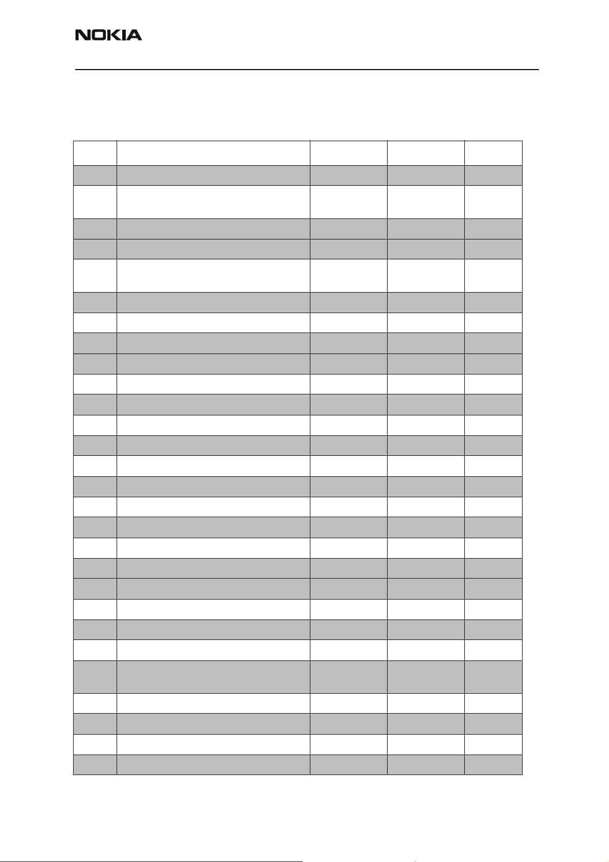
Step Step Name: Low Limits: High Limits: Unit:
1 TS Initial Current 5 100 mA
2 BB Flash Phone Pass/Fail-
Test
MS Off state Current 10 100 uA
3 MS Local Mode Current 30 70 mA
4 Write Phone Information Pass/Fail-
Test
5 ST DBUS 0 10
6ST CBUS 0 10
ST MBUS TX/RX 0 0
7 ST Aux DA 0 10
8 ST Ear Data 010
9 ST Sleep X 0 10
10 ST TX I DP 0 10
11 ST TX Q DP 0 10
12 ST MFI Loopback 0 10
13 ST Sleep Clock 0 10
14 ST Batman VHF PLL 0 10
15 ST Robin VHF PLL CELL 0 10
16 ST TX Detector CELL 0 10
ST Mode CDMA CELL RX 1 1
17 SN CELL PA Temp 200 400 ADC
18 SN CELL RX BB Filter 1 30
19 SN CELL RX DC Offset I 0 1023
20 SN CELL RX DC Offset Q 0 1023
21 PM AMPS RX Pass/Fail-
Test
22 SN AMPS RX BB Filter 1 14
23 SN AMPS RX DC Offset I 0 1023
24 SN AMPS RX DC Offset Q 0 1023
25 BB Cal ADC Gain 2.63 2.83
Issue 1 04/2003 Nokia Corporation Confidential Page 5
Page 6
RH-17
Troubleshooting — RF CCS Technical Documentation
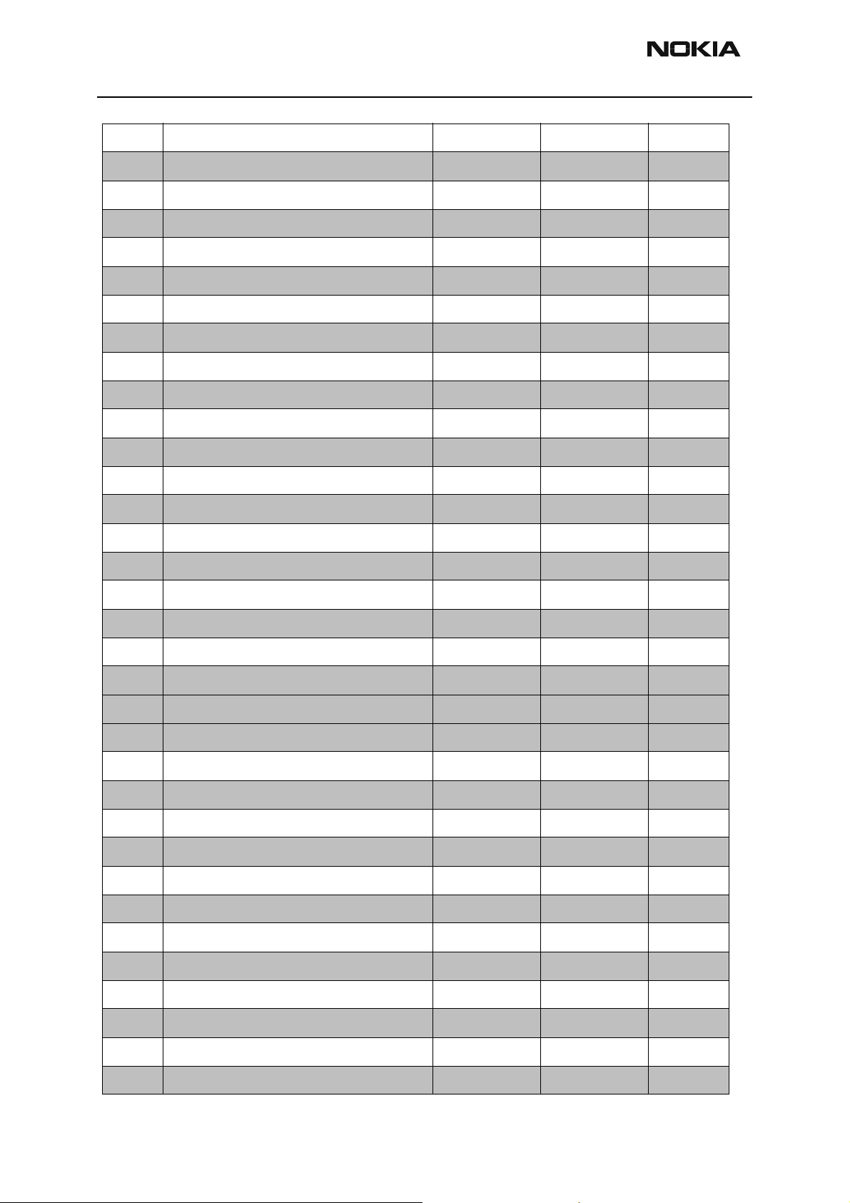
26 BB Cal ADC Offset -50 50
27 BB Cal ADC Vref 2.75 2.85
28 BB Cal BSI Gain 900 1100
29 BB Cal VBAT Gain 1.03 1.07
30 BB Cal VBAT Offset 2.4 2.6
31 BB Cal VCHAR Gain 5.7 6.3
32 BB Cal VCHAR Offset -0.2 0.2
33 BB Cal ICHAR Gain 400 450
34 BB Cal ICHAR Offset -50 50
35 BB Cal BTEMP Gain 2 2.3
36 TS TX Start-up Amplitude 5 20 dBm
37 TS TX Start-up Freq Delta -2500 2500
38 TS TX Start-up Current 300 600 mA
39 TN VCTCXO Frequency -150 150 Hz
40 TN TX IF AGC CELL Po(0) -30.5 -13.5 dBm
41 TN TX IF AGC CELL Po(1) -8 6 dBm
42 TN TX IF AGC CELL Po(2) 6.5 20.5 dBm
43 TN TX IF AGC CELL Po(3) 6.5 20.5 dBm
44 TN TX IF AGC CELL Po(4) 25 39 dBm
TN TX IF AGC CELL Po(5) 29 42 dBm
TN TX IF AGC CELL Po(6) 37 49 dBm
45 TN TX IF 11dBm Set CELL Po 10.75 11 .2 5 dBm
46 TN TX PA AGC CELL Po(0) -1 6.5 dBm
47 TN TX PA AGC CELL Po(1) 1 8.5 dBm
48 TN TX PA AGC CELL Po(2) 2 10.5 dBm
49 TN TX PA AGC CELL Po(3) 4 11 . 5 dBm
50 TN TX PA AGC CELL Po(4) 7 13 dBm
51 TN TX PA AGC CELL Po(5) 10.5 11 .5 dBm
52 TN TX RF AGC CELL Po(0) -41 -21 dBm
53 TN TX RF AGC CELL Po(1) -23.5 -7 dBm
54 TN TX RF AGC CELL Po(2) -10.5 3.5 dBm
55 TN TX RF AGC CELL Po(3) -3.5 9.5 dBm
56 TN TX RF AGC CELL Po(4) 0.5 11.5 dBm
57 TN GnSwchPnts Init RF GD AMPS 25 44.99
Page 6 Nokia Corporation Confidential Issue 1 04/2003
Page 7
RH-17
CCS Technical Documentation Troubleshooting — RF
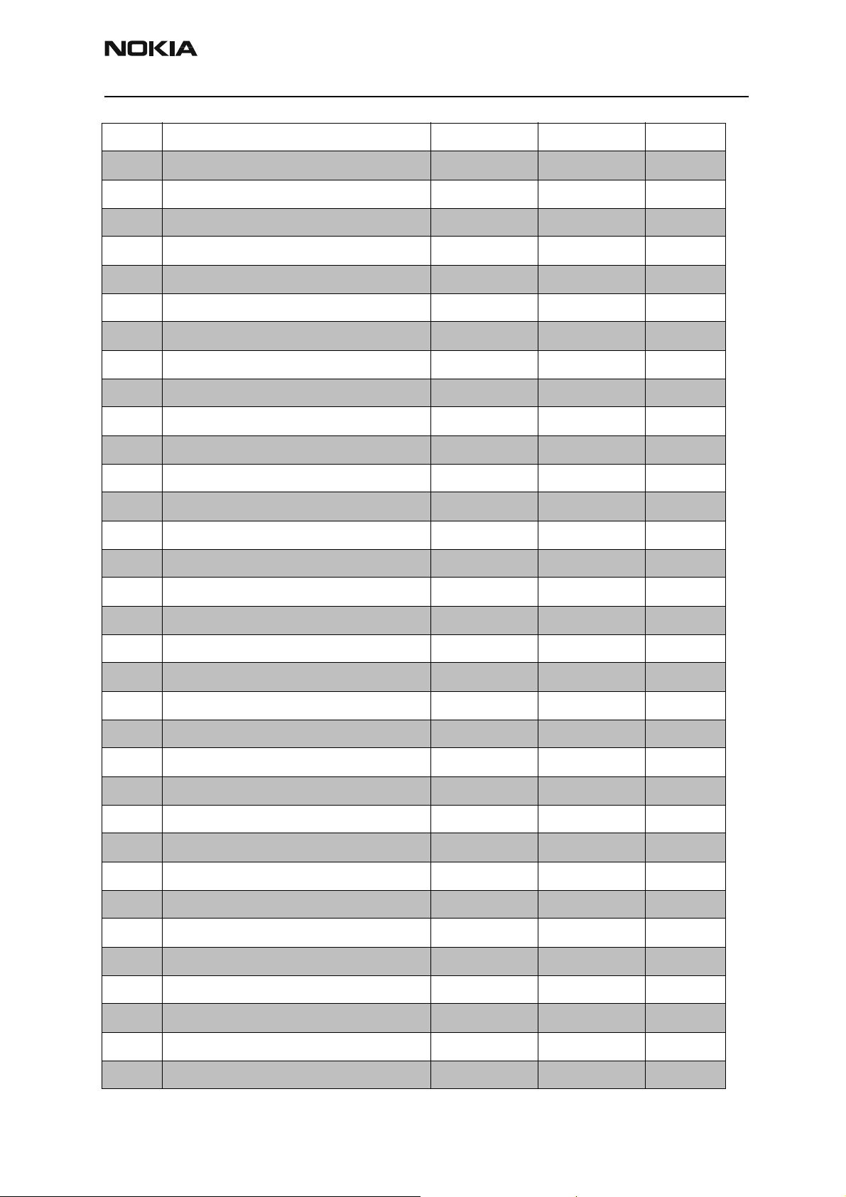
58 TN GnSwchPnts RF GD AMPS 0 100
59 TN GnSwchPnts Init RF GD CELL 25 44.99
60 TN GnSwchPnts RF GD CELL 0 100
61 TN TX Gain Comp CELL Po MD -8.25 -7.75 dBm
62 TN TX Gain Comp CELL Po LO -11.5 -4.5 dBm
63 TN TX Gain Comp CELL Po LM -11.0 -4.0 dBm
64 TN TX Gain Comp CELL Po ML -11.0 -4.0 dBm
65 TN TX Gain Comp CELL Po MH -10 -3 dBm
66 TN TX Gain Comp CELL Po HM -10 -2 dBm
67 TN TX Gain Comp CELL Po HI -13.5 -5 dBm
68 TN G_Offset_CELL_MD 2600 8000
69 TN TX LIM Po IS95 CELL LO 23.3 23.5 dBm
70 TN TX LIM Po IS95 CELL LM 23.6 23.8 dBm
71 TN TX LIM Po IS95 CELL ML 24.0 24.2 dBm
72 TN TX LIM Po IS95 CELL MD 24.4 24.6 dBm
73 TN TX LIM Po IS95 CELL MH 24.3 24.5 dBm
74 TN TX LIM Po IS95 CELL HM 24.2 24.4 dBm
75 TN TX LIM Po IS95 CELL HI 24.1 24.3 dBm
76 TN TX LIM Po IS2K CELL LO 23.3 23.5 dBm
77 TN TX LIM Po IS2K CELL LM 23.6 23.8 dBm
78 TN TX LIM Po IS2K CELL ML 24 24.2 dBm
79 TN TX LIM Po IS2K CELL MD 24.4 24.6 dBm
80 TN TX LIM Po IS2K CELL MH 24.3 24.5 dBm
81 TN TX LIM Po IS2K CELL HM 24.2 24.4 dBm
82 TN TX LIM Po IS2K CELL HI 24.1 24.3 dBm
83 TN TX LIM Loops CELL LO 0 10
84 TN TX LIM Loops CELL LM 0 10
85 TN TX LIM Loops CELL ML 0 10
86 TN TX LIM Loops CELL MD 0 10
87 TN TX LIM Loops CELL MH 0 10
88 TN TX LIM Loops CELL HM 0 10
89 TN TX LIM Loops CELL HI 0 10
90 TN TX LIM Loops CELL IS2K LO 0 10
91 TN TX LIM Loops CELL IS2K LM 0 10
Issue 1 04/2003 Nokia Corporation Confidential Page 7
Page 8
RH-17
Troubleshooting — RF CCS Technical Documentation
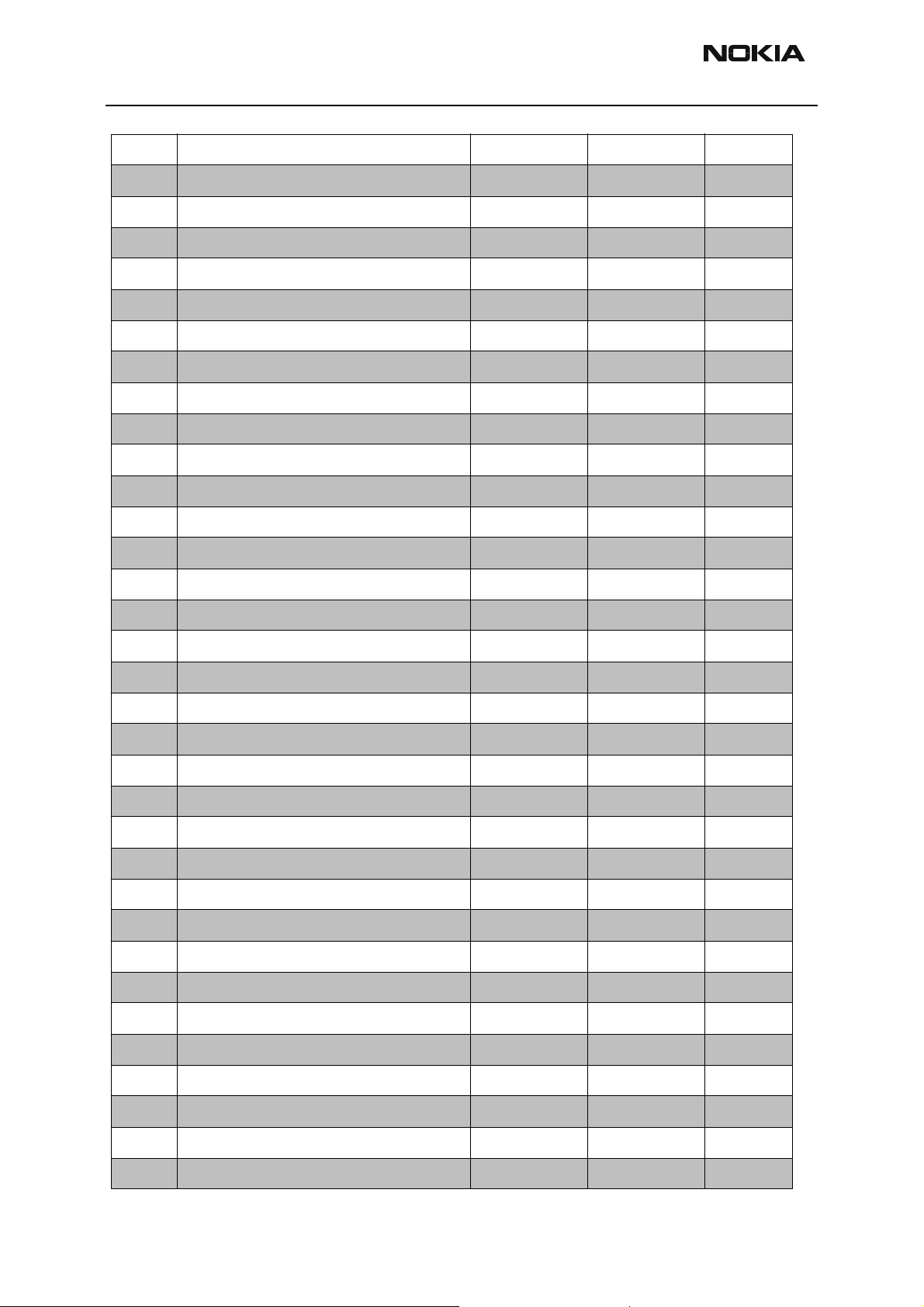
92 TN TX LIM Loops CELL IS2K ML 0 10
93 TN TX LIM Loops CELL IS2K MD 0 10
94 TN TX LIM Loops CELL IS2K MH 0 10
95 TN TX LIM Loops CELL IS2K HM 0 10
96 TN TX LIM Loops CELL IS2K HI 0 10
97 TS TX LIM MeasCount CELL 0 500
98 TS TX LIM TXdBCtr Delta CELL -32767 32767
99 TS TX LIM IS95 ADC CELL MD 550 850
100 TS ACPR CELL High Offset 44 75 dB
101 TS ACPR CELL Low Offset 44 75 dB
102 TS TX LIM Current CELL 600 1000 mA
103 TN AMPS PL2 Po LO 23.3 23.4 dBm
104 TN AMPS PL2 Po LM 23.6 23.8 dBm
105 TN AMPS PL2 Po ML 24.0 24.2 dBm
106 TN AMPS PL2 Po MD 24.4 24.6 dBm
107 TN AMPS PL2 Po MH 24.3 24.5 dBm
108 TN AMPS PL2 Po HM 24.2 24.4 dBm
109 TN AMPS PL2 Po HI 24.1 24.3 dBm
110 TN AMPS PL2 MeasCount 0 500
111 TN AMPS PL3 Po 23.3 24.1 dBm
112 TN AMPS PL4 Po 19.1 20.9 dBm
11 3 TN AMPS PL5 Po 15.1 16.9 dBm
114 TN AMPS PL6 Po 11.1 12.9 dBm
11 5 TN AMPS PL7 Po 7.3 8.7 dBm
116 TN AMPS PL8 Po ADC Data 4.5 7.5
11 7 TN AMPS Low PL MeasCount 0 500
118 TN TX DC Offset CarrierSup 35 120 dB
11 9 TN TX DC Offset Ref Po -30 30 dBm
120 TN TX DC Offset MeasCount 0 500
121 TN RX IF AGC RXdBCtr(0) 23584 30848
122 TN RX IF AGC RXdBCtr(1) 14000 18000
123 TN RX IF AGC RXdBCtr(2) 5900 8900
124 TN LNA AMPS LowGain 298 3652
125 TN LNA AMPS HighGain 4359 7713
Page 8 Nokia Corporation Confidential Issue 1 04/2003
Page 9
RH-17
CCS Technical Documentation Troubleshooting — RF
126 TN LNA CELL LO LowGain -601 4289
127 TN LNA CELL LM LowGain -601 4289
128 TN LNA CELL ML LowGain -601 4289
129 TN LNA CELL MD LowGain 423 3777
130 TN LNA CELL MH LowGain -601 4289
131 TN LNA CELL HM LowGain -601 4289
132 TN LNA CELL HI LowGain -601 4289
133 TN LNA CELL LO HighGain 3475 8365
134 TN LNA CELL LM HighGain 3475 8365
135 TN LNA CELL ML HighGain 3475 8365
136 TN LNA CELL MD HighGain 4499 7853
137 TN LNA CELL MH HighGain 3475 8365
138 TN LNA CELL HM HighGain 3475 8365
139 TN LNA CELL HI HighGain 3475 8365
140 NVD Write RF Params Pass/Fail-
Test
141 NVD Write Non RF Params Pass/Fail-
Test
Troubleshooting Summary
If TX power is low, turn on transmitter in local mode using Phoenix. Check:
1 Current (0.7 - 1 A for max power, mode and channel dependent),
2 Perform visual inspection of PWB under microscope to check proper placement,
rotation, and soldering of components.
3 Look for presence of TX signal on spectrum analyzer at the correct frequency. If
signal is not on frequency, check in 100 MHz span. If signal is present but off frequency, check synthesizer. If signal is not present, or present but low in amplitude, use probing Tables 1 through 7 to determine where in the chain the fault
occurs, with AGC PDMs set for known transmit power as listed in Table 1.
4 Check that AGC PDMs are set for desired TX power according to Table 1 and
ensure AGC voltages are correct.
5 According to Tables 2 and 3 (cell/AMPs), check the LOs for proper frequency and
amplitude.
6 Ensure power supplies to transmitter have correct voltage, as per Table 13.
Issue 1 04/2003 Nokia Corporation Confidential Page 9
Page 10
RH-17
Troubleshooting — RF CCS Technical Documentation
If Receiver is not working properly, turn on receiver in local mode using Phoenix and
check:
1 Turn on receiver with Phoenix, inject a signal into the receiver.
2 Check the RSSI level and AGC PDM according to Table 8.
3 Perform a visual inspection of the PWB under a microscope to check proper
placement, rotation, and soldering of components.
4 Use probing Tables 8 through 12 to measure signal levels of various points in the
chain and determine where in the chain the fault lies.
5 According to Tables 9, 10, and 12 check the LOs for proper frequency and ampli-
tude.
6 Ensure power supplies to receiver have correct voltage as per Table 13.
Page 10 Nokia Corporation Confidential Issue 1 04/2003
Page 11
RH-17
CCS Technical Documentation Troubleshooting — RF
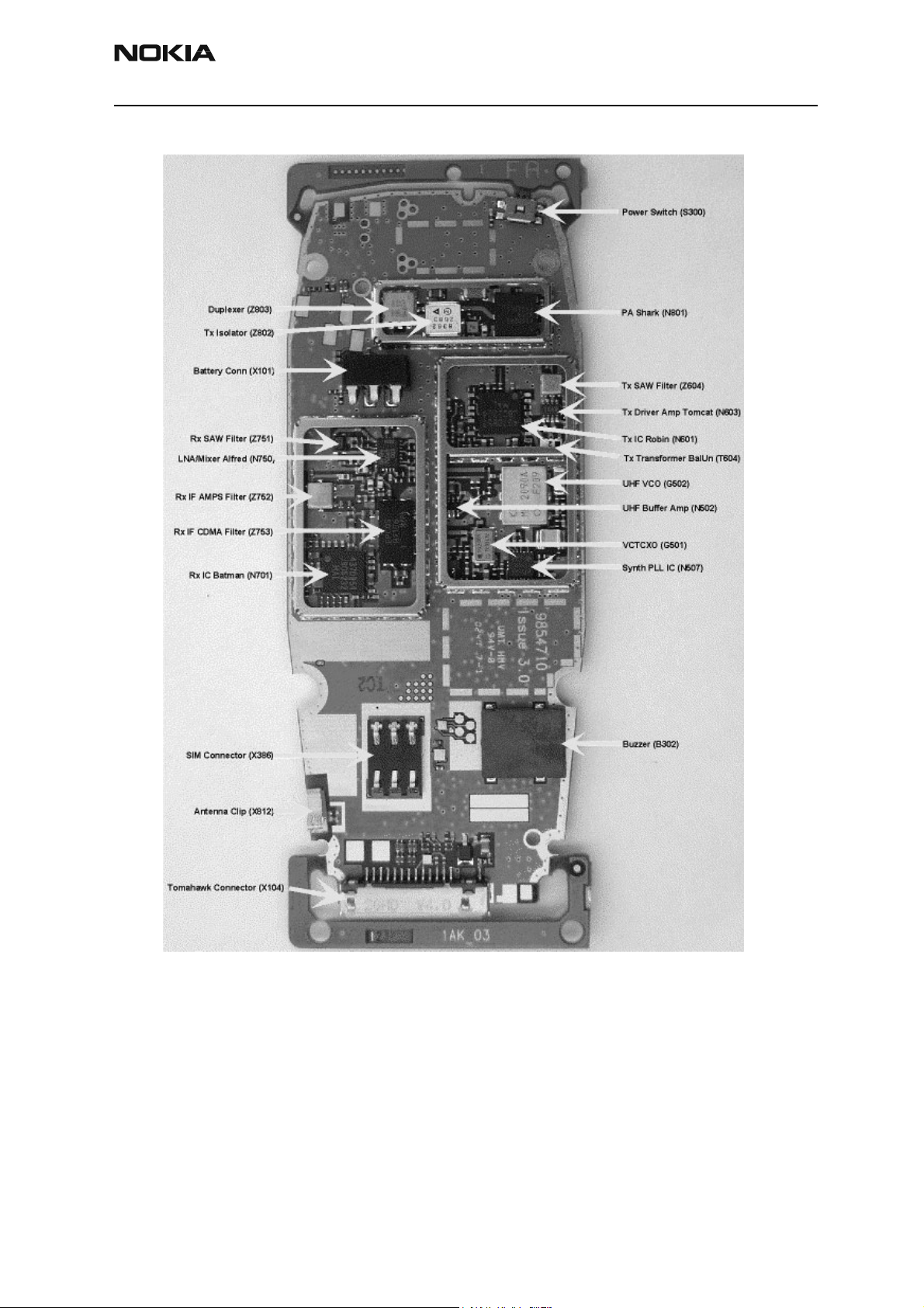
Figure 1: RH-17 PWB bottom (general placement)
Issue 1 04/2003 Nokia Corporation Confidential Page 11
Page 12
RH-17
Troubleshooting — RF CCS Technical Documentation
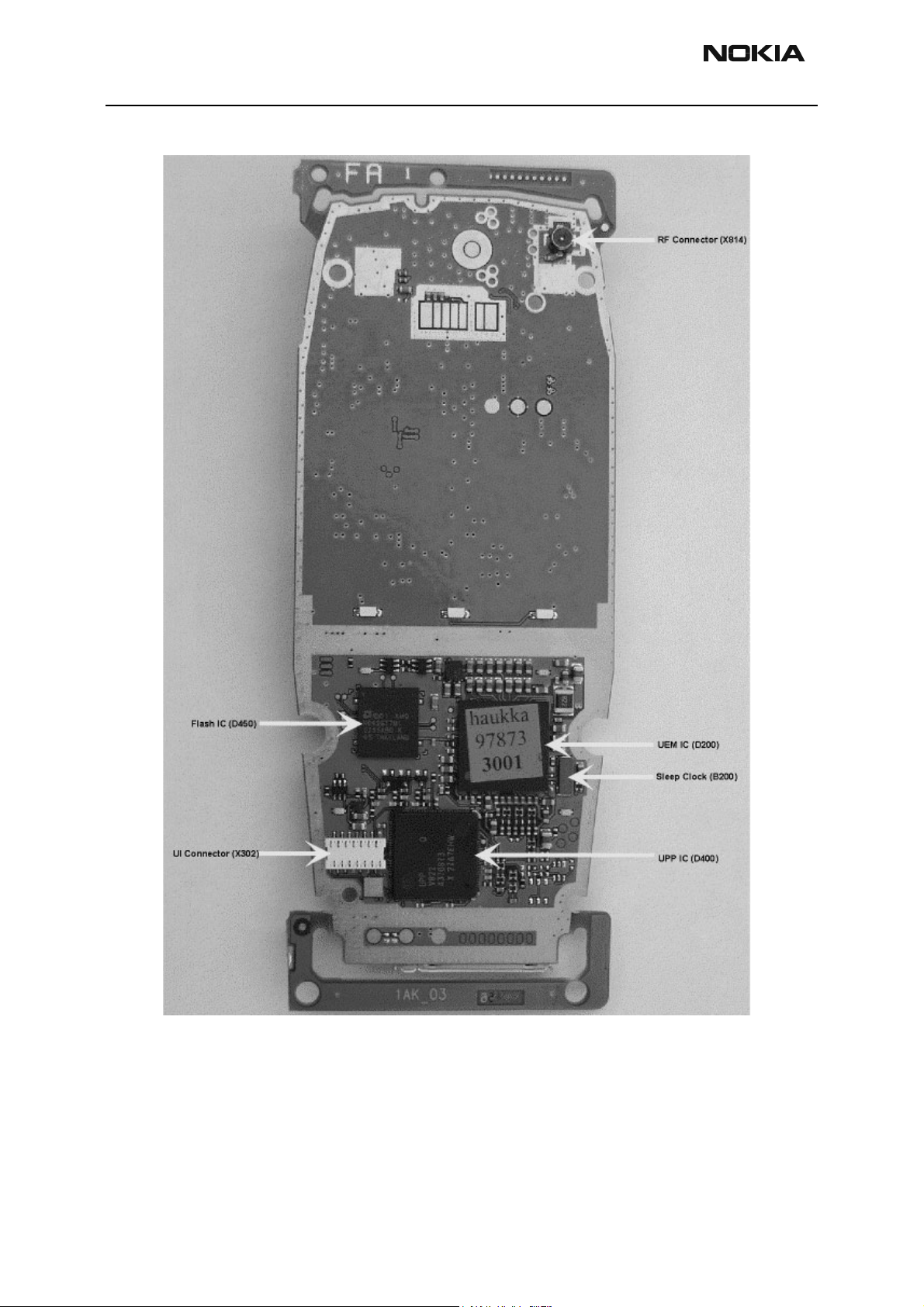
Figure 2: RH-17 PWB top (general placement)
Page 12 Nokia Corporation Confidential Issue 1 04/2003
Page 13

RH-17
CCS Technical Documentation Troubleshooting — RF
Tuning Description
Test 1 TS Initial Current
Description
Check initial current consumption at start-up to make sure phone is consuming correct
amount of current.
Explanation of Result
Phones current consumption is measured and should be between 5mA and 100 mA.
Manual Verification
Check using Power Supply and Multimeter, example follows. Power Off phone and follow
setup below to verify if phone’s current consumption is correct.
1 Positive Banana connector on Test Fixture to Power Supply +
2 Ground Banana connector on Test Fixture to | on Multimeter
3 Jumper cable between Power Supply (-) and Multimeter (input low)
4 Set Multimeter to measure current (DC|)
5 Multimeter should have an initial reading, this is the current being drawn by the
6 Place phone in Test Fixture
7 Press Power key to turn phone on
8 Observe current draw at Multimeter. It should be between 5.0mA and 100.0mA.
Troubleshooting
If phone drains all available current:
Check VBAT and do a visual inspection of all baseband ICs including orientation. VBAT
supplies the D200 (UEM), N603 (Tomcat), N801 (PA), X101, N100, B302, M300, N300,
and X470.
Text Fixture. Null out the Multimeter to Zero the reading.
If the phone has initial current consumption at start-up then powers down:
If, after a few seconds, all circuits power down, it is normally caused because the watchdog signal between UEM (200) and UPP (D400) has expired. Watchdog is used by the
phone for fault detection.
• Check voltage regulators for correct voltage. If voltage is low or not
present, check for shorts.
Issue 1 04/2003 Nokia Corporation Confidential Page 13
Page 14

RH-17
Troubleshooting — RF CCS Technical Documentation
VCORE - 1.50V @ C403
VIO - 1.8V @ C242
VANA - 2.8V @ C264
VFLASH1 - 2.8V @ C239
VR3 - 2.8V @ C256
• Check logic signals and clocks:
Power_OnX @ R301
UEMint - 2.80 Vdc @ test point J405
PURX - 2.80 Vdc @ test point J402
SleepX - 1.80 Vdc @ test point J403
Clk 19M2_UPP-19.2MHz @ C524
SleepClk - 32.768kHz @ J404
Test 2 BB Flash Phone
Description
The purpose of this test is to verify that the phone software was downloaded at panel
flash. If download was not successful, phone will try and flash for a second time.
Explanation of Result
Pass or Fail
Manual Verification
Manual flashing using Prommer Box and Phoenix at bench.
1 Make sure correct connection is configured at FPS-8. First, set up FPS-8 with
serial (AXS-4) and parallel cables. Next, power up box with 6-volt supply and
place communication cable XCS-4 between FPS-8 and Flash Adapter (FLA-44),
FLAL Fixture MJS-82, or JBV-1 (with adapter MJF-28).
2 Make sure that Phoenix’s connection is correct. In Phoenix, select File>Manage
Connections>Add>Mode to manual>Media to FBUS>Port NUM 1 or 2 (this is
dependent on Local PC com port selection)>Bit Rate to
115200>COMBOXDEF_MEDIA to FBUS; then Apply.
3 Check that Prommer Box FPS-8 is correctly configured. In Phoenix, go to Flash-
ing>FPS-8/FPS-8C Maintenance. Make sure current version is A2.10.
Page 14 Nokia Corporation Confidential Issue 1 04/2003
Page 15

RH-17
CCS Technical Documentation Troubleshooting — RF
4 Next, try and flash phone using correct SW version. In Phoenix: Flashing>FPS-8
Flash>Press Flash. Next select OK from pop-up screen. Under next screen, Flash
File Selection, choose Image File “set”. In correct directory where you store your
flash files (usually programs, then Nokia, Phoenix, Flash) select correct Flash SW
xxxxxxx.nep (if not sure what correct SW to use, file name should match SW in a
known good phone. To check this, take good phone in Phoenix and go Product>Phone Information and check MCU SW Version). Once correct SW file is
found, select OK. You will be prompted to save settings, select “yes”. Flashing
should begin at this point. For first time, set up of prommer this could take a few
minutes due to PC loading file to prommer RAM first. After first use, prommer
stores this in internal RAM and should proceed faster with subsequent phones
downloading of flash software. If phone passes, then more than likely a false fail.
If phone fails, read prommer failure code and use Code Sheet in TS.
Troubleshooting
Make sure phone has PSN and SW version is correct by checking Phone Information. Reference the following guides to TS flash problem: Haukka BB Operation doc, Prommer
Codes, and Flash Block Diagram.
Test 5 ST DBUS
Description
The purpose of this test is to verify that the connections between the DSP inside the UPP
and the UEM, via the DBUS, are intact. The DSP will write an arbitrary value to DBUS
General Control register in UEM; then DSP will read DBUS from General Control register
in UEM and valid repeatability.
Explanation of Result
Pass or Fail
Manual Verification
In Phoenix, put phone in Local Mode. Next, BB Self Tests - select ST_UEM_DBUS_TEST,
then Run.
Troubleshooting
Connections tested at UPP: DBUSDA (pad L3) check test point J414, DBUSCLK (pad K3)
check test point J413, DBUSEN1X (pad J3) check test point J415. At UEM: DBUSDA (pad
A11), DBUSCLK (pad D10), and DBUSENX (pad B10). Bus interface name is RFCONVCTRL(2:0).
Test 6 ST CBUS
Description
The purpose of this test is to verify that the connections between the MCU inside the
UPP and the UEM, via the CBUS, are intact. The MCU will read CBusADCR register and
verify UEM chip version is valid.
Issue 1 04/2003 Nokia Corporation Confidential Page 15
Page 16
RH-17
Troubleshooting — RF CCS Technical Documentation
Explanation of Result
Pass or Fail
Manual Verification
In Phoenix, put phone in Local Mode; next, BB Self Tests - select ST_UEM_CBUS_IF_TEST,
then Run.
Troubleshooting
Connections tested at UPP: CBUSDA (pad G2) check test point J407, CBUSCLK (padG1)
check test point J406, CBUSENX (pad F3) check test point J408. At UEM: CBUSDA (pad
B7), CBUSCLK (pad A8), and CBUSENX (pad C8). Bus interface name is AUDUEMCTRL
(3:0).
Test 7 ST Aux DA
Description
The purpose of this test is to verify the AUXD and UEMINT data connections between the
UPP and the UEM are intact. MCU will set the UEM looptest mode by programming the
Loop Test bit in the CBUS General Control 2 register. Next, DSP will write a word to AuxD
register, thus causing a rising edge on the AuxD line. MCU will verify that UEMInt occurs.
Explanation of Result
Pass or Fail
Manual Verification
In Phoenix, put phone in Local Mode; next BB Self Tests - select
ST_AUX_DA_LOOP_TEST; then Run.
Troubleshooting
Connections tested: 1) UPP: AUXDA (pad L2) via bus interface RFCONVDA(5) to UEM:
AUXDA (pad D11). 2) UPP: UEMINT (pad J2) check test point J405, via bus interface
AUDUEMCTRL(0) to UEM; UEMINT (pad A10).
Test 8 ST EAR Data
Description
The purpose of this test is to verify the EAR and MIC data connections between the UPP
and the UEM are intact. MCU will set the UEM looptest mode by programming the Loop
Test bit in the CBUS General Control 2 register. Next, DSP will write an arbitrary pattern
to CodexRx register and then read the data from the Codec Tx register.
Explanation of Result
Pass or Fail
Manual Verification
In Phoenix, put phone in Local Mode. Next, BB Self Tests - select
Page 16 Nokia Corporation Confidential Issue 1 04/2003
Page 17

RH-17
CCS Technical Documentation Troubleshooting — RF
ST_EAR_DATA_LOOP_TEST, then Run.
Troubleshooting
Connections tested at UPP: EARDATA (pad B6), MICDATA (pad A6), and at UEM: EARDATA
(pad E2), MICDATA (pad F2). Bus interface name is AUDIODATA (1:0).
Test 9 ST SleeepX
Description
The purpose of this test is to verify the Sleep connection between the UPP and the UEM
is intact. This function tests the connection of pin_out and pin_in signals between UPP
and UEM. The result depends on functionality of UEM loopback modes and condition of
signal lines. The MCU will set UEM in looptest mode by programming via CBUS. MCU will
then read sleep clock counter registers and store value. MCU then toggles SleepX signal
High then Low and reads counters again. Expected value is 1 higher than previous count.
Explanation of Result
Pass or Fail
Manual Verification
In Phoenix, put phone in Local Mode. Next, BB Self Tests - select
ST_SLEEP_X_LOOP_TEST, then Run.
Troubleshooting
Connections tested are CBUS see Test 6, Sleepclock (J404) at UEM (D9) to UPP (H3).
SleepX (J403) at UEM (pad B11) from UPP (pad L1). Bus interface between UPP and UEM
is PUSL (2:0). Check also at UEM the OSCCAP (C234).
Test 10 ST TX / DP
Description
To verify that the Tx/Rx | lines between UPP and UEM are intact. MCU will set UEM into
Looptest mode by programming the Loop Test bit via CBUS General Control 2 register.
DSP will set Parallel-series bypass switches for both Rx and Tx in the MFI block of the
UPP by programming the TxBypass and RxBypass bits in the MFI Control Register. DSP
will write arbitrary value to TxRam of MFI, then DSP will read this data from RxRAM of
the MFI.
Explanation of Result
Pass or Fail
Manual Verification
In Phoenix, put phone in Local Mode. Next, BB Self Tests - select ST_TX_IDP_LOOP_TEST,
then Run.
Troubleshooting
Connections tested are CBUS see Test 6, Connections tested at UPP: RXID (pad L4), TXID
Issue 1 04/2003 Nokia Corporation Confidential Page 17
Page 18

RH-17
Troubleshooting — RF CCS Technical Documentation
(pad M2) and at UEM: RXID (pad C11), TXID (pad A12). Bus interface name is RFCONVDA
(5:0).
Test 11 ST TX Q DP
Description
To verify that the Tx/Rx Q lines between UPP and UEM are intact.
Explanation of Result
Pass or Fail
Manual Verification
In Phoenix, put phone in Local Mode. Next, BB Self Tests - select
ST_TX_IQ_DP_LOOP_TEST, then Run.
Troubleshooting
Connections tested are CBUS see Test 7. Connections tested at UPP: RXQD (pad N4),
TXQD (pad N2), and at UEM: RXQD (pad A14), TXQD (pad B12). Bus interface name is
RFCONVDA (5:0).
Test 12 ST MIF Loopback
Description
The purpose of this test is to verify that the Tx/Rx IQ paths inside the MFI block of the
UPP are intact. DSP will swt IQSTWrap in MFI Control Register. Next, DSP will set six of
the TX and Rx buffers to be the same. Sets Serial-Parallel bypass switches On. DSP will
write a varying pattern to both halves of the Tx buffer, then read Rx buffer and verify
data written is data received.
NOTE: This test does not test the connectivity between any two points in the HW (nodes
inside of a chip do not qualify for connectivity). This test ascertains the cause of the UEM
IQ Loopback Selftest failure, and determines whether the UPP or the UEM or the connection between them caused the UEM IQ to Loopback Selftest fail.
Explanation of Result
Pass or Fail
Manual Verification
In Phoenix, put phone in Local mode: Next, BB Self Tests - select
ST_MFI_IQ_LOOPBACK_TEST, then Run.
Troubleshooting
Connections tested are UPP only. If this test passes and Test 11 fails, then the problem is
in UEM. If both Test 11 and Test 12 fail, the problem is in UPP.
Page 18 Nokia Corporation Confidential Issue 1 04/2003
Page 19

RH-17
CCS Technical Documentation Troubleshooting — RF
Test 13 ST Sleep Clock
Description
The purpose of this test is to verify connections from 32kHz oscillator to the UEM, then
from UEM to SleepClk to the UPP. Also tested is AFCOUT of the UEM to the VCTCXO, and
from VCTCXO to RF clock to UPP are intact. UPP sets AFCR for UEM to set AFCOUT to mid
range. Next, DSP will measure how many 19.2MHz clock cycles are present in 1024
cycles of the 32kHz clock. Next, AFCOUT is set to maximum value by writing to AFCR in
UEM. Again measurement is taken as previously mentioned. The two measurements are
subtracted. Then, AFCOUT is set to minimum value and again measured and compared to
mid-value results. Expected values are validated by pass or fail.
Explanation of Result
Pass or Fail
Manual Verification
In Phoenix, put phone in Local Mode. Next, BB Self Tests - select
ST_APOLL_SLEEP_CLK_TEST, then Run.
Troubleshooting
Connections tested are DBUS (see Test 5), VCTCXO circuit including AFC control voltage
from UEM, Sleepclock at UEM, and also RFCLK to UPP via V500 and C524. Check also at
UEM the OSCCAP (C234).
Test 14 ST Batman VHFPLL
Description
This is one of the phone’s self tests which gives either a pass or fail result only. The VHF
PLL is inside the Batman IC. The phone checks the VHFPLL’s lock detect bit. If this bit
indicates that the PLL is unlocked, the test will fail.
Explanation of Result
Pass or Fail
Manual Verification
Turn on the Cell receiver to any channel and probe at C702 (probing point TP49 in
Table 10 using an RF probe connected to a spectrum analyzer tuned to 256.2MHz. If the
PLL is locked, it will be stable in frequency. If it is unlocked, you may have to use a wide
span, so see if it may be far off frequency.
Troubleshooting
First check that V701 has the proper orientation, then check C701, C714, R703, R702,
C715, R704, C716, L701, and C702. Also, check power supplies to Batman, particularly
check for 2.7v on VR5 at C710, and on VR7 at C708, and check for 1.8v on VIO. Next
check if CLK 19M2_B (C512) the reference frequency for PLL is at 19.2MHz. If no fault is
found, replace N701 (Batman).
Issue 1 04/2003 Nokia Corporation Confidential Page 19
Page 20

RH-17
Troubleshooting — RF CCS Technical Documentation
Test 15 ST Robin VHF PLL CELL
Description
This is one of the phone’s self-tests which gives either a pass or fail result. The VHFPLL is
inside the Robin IC. The phone checks the VHFPLL’s lock detect bit. If this bit indicates
that the PLL is unlocked, the test will fail.
Explanation of Result
Pass or Fail
Manual Verification
Turn on the Cell CDMA transmitter to any channel and probe at C638 (probing point
TP27 in Table 2) using an RF probe connected to a spectrum analyzer tuned to 345.2MHz.
If th PLL is locked, it will be stable in frequency. If it is unlocked, you may have to use a
wide span to see it since it may be far off frequency.
Troubleshooting
First, check that V601 and V602 have the proper orientation, then check C612, C613,
R607, R605, C632, R606, C638, L611, C631, C630, C629, C637, R609, C618, and R613.
Check power supplies to N601 (Robin) and ensure there is 2.7v on VR3 and VR6, and 1.8v
on VIO (Table 13). Next, check if CLK 19M2_R (C513) the reference frequency for PLL is
at 19.2MHz. If no problems are found, replace Robin.
Test 16 ST TX Detector CELL
Description
This is one of the phone’s self-tests which gives either a pass or fail result only. The
phone transmits at several power levels and checks the ADC value of the power detector.
The ADC value is measured first for a set of AGC values, then each AGC value is changed
one at a time to make sure that the ADC changes as each AGC value is changed individually.
Explanation of Result
Pass or Fail
Manual Verification
Using Main Mode: turn on the Cell CDMA TX with channel set to 384, and turn on IS95
modulation using CDMA control.
Using the PDM window, set:
TX_IF_AGC to -100
TX_RF_AGC to -512
PA_AGC to +511
Page 20 Nokia Corporation Confidential Issue 1 04/2003
Page 21

RH-17
CCS Technical Documentation Troubleshooting — RF
Record the TX signal power from the antenna connector using a spectrum analyzer centered at 836.52Mhz. (The self-test measures the power detector reading instead, but at
the present time this cannot be done with Phoenix, therefore an easy way to check functionality without removing the covers is to check transmitted power. If the covers are
removed, the voltage on PWR_OUT, at probing point J603 can be measured.) Transmitted
power should be greater than 24dBm. (PWR_OUT greater than 1.91v, which corresponds
to the power detector ADC=700).
For each of the next three cases, TX power should be less than 24dBm (less than 1.91v on
PWR_OUT.
1. TX_IF_AGC to -80
TX_RF_AGC to -512,
PA_AGC to -512
2. TX_IF_AGC to +511,
TX_RF_AGC to -512,
PA_AGC to +511
3. TX_IF_AGC to -80
TX_RF_AGC to +511
PA_AGC to +511.
Troubleshooting
If there is a failure associated with only some of the cases above, check the AGC voltages
and components of the associated PDMs as described in Table 1. For problems with the IF
or RF AGC, also check Robin and supporting components. For PA AGC problems, also
check the PA and supporting components. If all of the above cases fail, troubleshoot the
TX chain as described in Probing/Troubleshooting Tables. If all the output powers are
passing, then perhaps the test is failing because the ADC voltage is wrong (which at this
point we cannot read, so we are measuring the actual output power). This can be verified
by measuring the voltage on the PWROUT probing point J603, the limit is 1.64v. If the
voltages are wrong, then check the power detector at R801, L801, R805, and C807, and
also Robin. If the voltages are correct and it still fails, check the UEM (D200).
Test 17 SN CELL PA Temp
Description
This is one of the phone’s self-tunings, which reads the ADC voltage of a thermistor
R808, and checks to make sure the phone is at room temperature. The reason for this is
that we don’t want to tune a phone while it is hot or cold.
Explanation of Result
The phone reports the ADC voltage value of the thermistor, and it should be within the
limits.
Manual Verification
Ensure the phone is cool by letting it cool down for several minutes, and retest, keeping
Issue 1 04/2003 Nokia Corporation Confidential Page 21
Page 22

RH-17
Troubleshooting — RF CCS Technical Documentation
in mind that if there is a short circuit on the board, then it will get hot very quickly. In
Phoenix, go to ADC readings and verify Power Amplifier Temperature, ADC value will go
down as Temperature goes up.
Troubleshooting
If the phone was recently transmitting in Cell band at full power for an extended period
of time, it is probably hot for that reason. Let it cool down for a few minutes, then try
again. If it still fails, there may either be a short on the board or else a problem with the
PA Temp circuitry. To check PA Temp circuitry, check R808, C231, R207, and D200. If a
short is suspected, check the PA (N801).
Test 18 SN CELL RX BB Filter
Description
This is one of the phone’s self-tunings, which tunes the lowpass filter in the Batman IC
(N701), in cell CDMA mode.
Explanation of Result
This self-tuning returns one of the filters tuned parameters, which should be within the
limits.
Manual Verification
Use Batch Tuning window in Phoenix, select RF Tunings and check value.
Troubleshooting
Check Batman (N701) and supporting components.
Test 19 and 20 SN Cell RX DC Offset I (or Q)
Description
This is one of the phone’s self-tunings which measures and adjusts the cell band CDMA
receiver DC offsets until they are within the limits.
Explanation of Result
The DC offset is returned for I (or Q).
Manual Verification
Use Batch Tuning window in Phoenix, select RF Tunings and check value.
Troubleshooting
In Phoenix, put phone in local mode, then CDMA RX. Check voltage at Batman (N701) at
test points TP45-TP48 and supporting components at Batman IC.
Test 22 SN AMPS RX BB Filter
Description
This is one of the phone’s self-tunings, which tunes the lowpass filter in the Batman IC
Page 22 Nokia Corporation Confidential Issue 1 04/2003
Page 23

RH-17
CCS Technical Documentation Troubleshooting — RF
(N701) in AMPS mode.
Explanation of Result
Use Batch Tuning window in Phoenix, select RF Tunings and check value.
Manual Verification
Use RF Tuning window in Phoenix, set mode to “self tune” and choose this tuning.
Troubleshooting
Check Batman (N701) and supporting components.
Test 23 and 24 SN AMPS RX DC Offset I (or Q)
Description
This is one of the phone’s self-tunings which measures and adjusts the cell band AMPS
receiver DC offsets until they are within the limits.
Explanation of Result
The DC offset is returned for I (or Q).
Manual Verification
Use Batch Tuning window in Phoenix, select RF Tunings and check value.
Troubleshooting
In Phoenix, put phone in local mode, then AMPS RX. Check voltage at Batman (N701) at
test points TP45-TP48 and supporting components at Batman IC.
Test 25 - 27 BB Cal ADC Gain
Description
This calibration trains the BB ADC to two known voltage inputs. Because of the inaccuracy of an analog-to-digital converter, it must be calibrated using known values. Once
values are established, phone will be able to calculate the other ADC calibrations accurately. Converter gain and offset parameters are calculated by measuring a voltage input
on BSI line of 0.7 Vdc and 2.1 Vdc. Also, some calibrations use the reference voltage V
It is calculated from offset and gain: V
REF
= offset + 1023 x gain.
REF
.
Explanation of Result
ADC Gain, Offset and Vref values
Manual Verification
In Phoenix, set phone to local mode then EM Calibration. Press read from phone. Gain
factor is 0.0001 mV/bit, Offset is measured in mV.
Troubleshooting
Check the BSI components X101, C109, C230, R206, and R203. Check that VFLASH volt-
Issue 1 04/2003 Nokia Corporation Confidential Page 23
Page 24

RH-17
Troubleshooting — RF CCS Technical Documentation
age is at 2.80 Vdc. Baseband components D200, D400, and D450 are soldered and
aligned correctly.
NOTE: All BB calibrations must be performed whenever UEM (D200) is replaced. In other
words, alignment is necessary at ATE.
Test 28 BB Cal BSI Gain
Description
This baseband calibration teaches the ADC what a 68k ohms emerges at the BSI pin.
Explanation of Result
BSI Gain ADC factor
Manual Verification
In Phoenix, set phone to local mode, then EM Calibration. Press read from phone.
Troubleshooting
BSI resistor value varies, dependent on fixture being used (e.g., JBV-1 (with adapter MJF-
28), FLA-44 or MJS-82. Check the BSI components X101, C109, C230, R206, and R203.
Check that VFLASH voltage is at 2.80Vdc. Baseband components D200, D400, and D450
are soldered and aligned correctly.
Test 29 BB Cal VBAT Gain
Description
This baseband calibration teaches the ADC what two different voltage inputs look like.
Lower known voltage input is 3.1 Vdc and higher input is 4.2 Vdc. This voltage-scaler circuit is used to form the voltage into the proper range.
Explanation of Result
The gain factor is a result of scaled value and the global value determined in Test 25 and
used to calculate VBAT Gain.
Manual Verification
In Phoenix, set phone to local mode, then EM Calibration. Press read from phone.
Troubleshooting
Check Battery Connector X101, baseband components D200, D400, and D450 are soldered and aligned correctly. Remember that this gain factor is determined using Test 25
as a reference. Make sure it was within limits also.
Test 30 BB Cal VBAT Offset
Description
This baseband calibration teaches the ADC what two different voltage inputs look like.
Lower known voltage input is 3.1 Vdc and higher input is 4.2 Vdc. This voltage-scaler cir-
Page 24 Nokia Corporation Confidential Issue 1 04/2003
Page 25

RH-17
CCS Technical Documentation Troubleshooting — RF
cuit is used to form the voltage into the proper range.
Explanation of Result
The offset is a result of scaled value and global value determined in Test 26 and used to
calculate VBAT Offset.
Manual Verification
In Phoenix, set phone to local mode then EM Calibration. Press read from phone.
Troubleshooting
Check Battery Connector X101, baseband components D200, D400, and D450 are soldered and aligned correctly. Remember that this gain factor is determined using Test 26
as a reference. Make sure it was within limits too.
Test 31 BB Cal VCHAR Gain
Description:
This baseband calibration teaches the ADC what two different voltage inputs look like.
Lower known voltage input is 3.0 Vdc and higher input is 8.4 Vdc.
Explanation of Result:
The gain factor is a result of the two voltages and the global value determined in Test 25
and used to calculate VCHAR Gain.
Manual Verification:
In Phoenix set phone to local mode then EM Calibration. Press read from phone.
Troubleshooting:
For production the VCHAR voltage is sent to galvanic pads on the PWB. Check for solder
bridge on X104, fuse F100, L100, C106 and V100. Remember that this gain factor is
determined using Test 25 as a reference, make sure it was within limits also.
Test 32 BB Cal VCHAR Offset
Description
This baseband calibration teaches the ADC what two different voltage inputs look like.
Lower known voltage input is 3.0 Vdc and higher input is 8.4 Vdc.
Explanation of Result:
The offset is a result of the two current limit values and the global value determined in
Test 26 and used to calculate VCHAR offset.
Manual Verification:
In Phoenix set phone to local mode then EM Calibration. Press read from phone.
Issue 1 04/2003 Nokia Corporation Confidential Page 25
Page 26

RH-17
Troubleshooting — RF CCS Technical Documentation
Troubleshooting:
For production the VCHAR voltage is sent to galvanic pads on the PWB. Check for solder
bridge on X104, fuse F100, L100, C106 and V100. Remember that this gain factor is
determined using Test 26 as a reference, make sure it was within limits also.
Test 33 BB Cal ICHAR Gain
Description:
This baseband calibration teaches the ADC what two different charger current inputs
look like. Voltage input is at 6.0 Vdc at two different current limits, lower being limited
to 200 mA, higher current limit is set at 800 mA. Then PCI command to instruct phone to
turn on charger circuitry.
Explanation of Result:
The gain factor is a result of the two current limits along with global value determined
in Test 25 which is then used to calculate ICHAR Gain.
Manual Verification:
In Phoenix set phone to local mode then EM Calibration. Press read from phone.
Troubleshooting:
For production the VCHAR voltage is sent to galvanic pads on the PWB. Check current
sensing resistor R200 then D200, where the charging circuitry resides. Remember that
this gain factor is determined using Test 25 as a reference, make sure it was within limits
also.
Test 34 BB Cal ICHAR Offset
Description:
This baseband calibration teaches the ADC what two different charger current inputs
look like. Voltage input is at 6.0 Vdc at two different current limits, lower being limited
to 200 mA, higher current limit is set at 800 mA. Then PCI command to instruct phone to
turn on charger circuitry.
Explanation of Result:
The offset is a result of the two current limits along with global value determined in Test
26 which is then used to calculate ICHAR offset.
Manual Verification:
In Phoenix set phone to local mode then EM Calibration. Press read from phone.
Troubleshooting:
For production the VCHAR voltage is sent to galvanic pads on the PWB. Check current
sensing resistor R200 then D200, where the charging circuitry resides. Remember that
this gain factor is determined using Test 26 as a reference, make sure it was within limits
also.
Page 26 Nokia Corporation Confidential Issue 1 04/2003
Page 27

RH-17
CCS Technical Documentation Troubleshooting — RF
Test 35 BB Cal BTEMP Gain
Description
Explanation of Result
Manual Verification
Troubleshooting
Test 36 Test TX Start up Amplitude Limits [5,20]
Description:
This test turns on the AMPS transmitter and checks for the presence of a TX signal with
an amplitude within a specified range. A wide range is allowed since the transmitter is
not tuned yet.
Explanation of Result:
Amplitude of TX signal.
Manual Verification:
Set the phone to local mode and turn on the AMPS transmitter set to channel 384. Set
the PDM values as listed in Table 1 for AMPS Power Level 5. Look for an output signal at
836.52 MHz with an amplitude within the limits. The frequency of the signal may not be
accurate since the VCTCXO has not been tuned yet.
Troubleshooting:
Check proper placement, rotation and soldering of the components in the TX chain.
Check for the presence of LO tones as listed in Table 2. Check for presence of a TX signal
at each point in the TX chain, probing according to Table 2.
Test 38 Test TX Start up Current Limits [300,600]
Description:
This test turns on the AMPS transmitter and measures current of the whole phone, which
can detect some assembly errors.
Explanation of Result:
Current in milliamps.
Manual Verification:
Set the phone to local mode and turn on the AMPS transmitter PL5. Set the PDM values
Issue 1 04/2003 Nokia Corporation Confidential Page 27
Page 28

RH-17
Troubleshooting — RF CCS Technical Documentation
as listed in Table 1 for AMPS Power Level 5. Read the phone's current on the power supply and check to see that it is within the limits. If the power supply does not display current draw, use a current meter in series with the phone. If the phone powers down when
the mode is set, it may be that the phone is drawing more current than the current limit
setting on the power supply.
Troubleshooting:
If current is very high, there may be a short circuit on the phone caused by a solder
bridge, a failed component that is internally shorted, a component placed with the
wrong rotation which shorts two nodes that shouldn't be, or some other reason. A visual
inspection can find solder bridges or wrong component rotations. A failed component
can be found by functional tests of the phone's sub-blocks.
Test 39 TN VCTCXO Frequency Limits [-150, 150]
Description:
The purpose of this tuning is to determine what the AFC DAC value needs to be in order
to center the VCTCXO frequency. The CDMA transmitter is turned on and no TX baseband
modulation is provided. The carrier is then centered in frequency. This is done to the carrier after it has been mixed up to 836.52 MHz, since it's easier to measure the tolerance
of 1 ppm at 836.52 MHz than it is at 19.2 MHz. Additionally the tone at 836.52 MHz can
be measured without taking the phone apart.
Explanation of Result:
The result is a frequency offset in Hz of the 836.52 MHz carrier which must be within +/
- 150 Hz.
Manual Verification:
Using the RF Main Mode window in Phoenix, turn on the CDMA transmitter, and set it to
channel 384. Do not add any modulation(Rho).
Using the RF Batch Tuning window, you can check the VCTCXO tuning value. Look for a
transmitted tone on the spectrum analyzer at 836.52 MHz. If no tone is present, proceed
to troubleshooting section.
Go to Phoenix PDM Control and follow instructions that follow. Center the carrier to
within +/- 150 Hz of 836.52 MHz. (If sidetones are present, be careful to center the carrier and not one of the sidetones, which will probably have a higher amplitude than the
carrier.) The values you enter in the "values" edit box are the AFC values which control
the VCTCXO frequency. Start with a value of 0, then adjust until it is centered, staying
within the limits.
Troubleshooting:
If there is no tone, probe pin 3 of G501 for a tone at 19.2 MHz. If this is not present
check power supplies, particularly ensure 2.7v on VCTCXO Vcc pin, pin 4 of G501. Also
check the control pin, pin 1 of G501, for a voltage between 0.4 and 2.7 v. If the voltages
are correct, and soldering of all G501 terminals is correct, replace G501. If 19.2 MHz tone
Page 28 Nokia Corporation Confidential Issue 1 04/2003
Page 29

RH-17
CCS Technical Documentation Troubleshooting — RF
is present but tone at 836.52 MHz is not, troubleshoot CDMA TX chain as described in
Tables 2 and 3.
If the carrier is present but it cannot be centered, there is a hardware problem. Check
Table 7.
In the following procedure, performing frequency centering on the RF carrier at 836.52
MHz will detect frequency errors due to the VCTCXO and supporting hardware, which
will be the majority of the problems, but will not detect frequency errors due to the
hardware that uses VCTCXO tone at 19.2 MHz as a reference for VHF PLL's. Check then
the VHF and UHF LO's should be at correct frequency. Since this will be time consuming
and will probably only account for a small percentage of the failures, it is not recommended unless the situation justifies the time spent. The VHF LO is inside the Robin IC
(N601) and troubleshooting of the cell UHF LO is according to Table 5.
If the carrier cannot be centered, check to see if you can adjust to 2.2v on pin 1 of G501.
If you can, within the PDM range of +/- 150, then the circuitry that delivers the voltage
is working correctly, and the VCTCXO has a problem. Troubleshoot it as described in the
previous section. If you cannot adjust to 2.2v within the accepted range, then the AFC
circuitry has a problem. Troubleshoot it as described in the previous section.
In the case that there is a fault with both the AFC circuitry and the VCTCXO, then several
combinations of the previously described conditions are possible. Start by ensuring 2.2v
on pin 1 of G501 using a PDM within the range +/- 150, then center the tone.
Test 40 - 44 TN TX IF AGC Cell Po (0) [or (1), (2), (3), (4), (5), (6)]
Description:
The IF gain curve is characterized by varying the TX_IF_AGC and measuring the transmit
power.
Explanation of Result:
The results are TX power readings in dBm of the transmitted signal corresponding to
given PDM settings of the Cell TX IF AGC.
C) Manual Verification:
Set the phone in local mode, then program it to Cell CDMA RX/TX mode on channel 384.
Set modulation to IS95 voice in CDMA Control.
Set the Cell PA PDM to +218 decimal and the TX RF AGC to -512 decimal using the sliders in the PDM window under the RF menu.
Change the TX_IF_AGC to the settings in the following table, and measure the TX power
levels, checking to see that they are within the specified range.
Issue 1 04/2003 Nokia Corporation Confidential Page 29
Page 30

RH-17
Troubleshooting — RF CCS Technical Documentation
PDM for TX IF AGC
(a) +388 decimal -27.5 - 13.5
(b) +228 -8.0 - 6.0
(c) 163 6.5 - 20.5
(d) 0 6.5 - 20.5
PChange the TX_RF_AGC PDM to +511. Leave the TX_IF_AGC at 0 and the PA_AGC at
+218. Measure the output power. Subtract this power from the power measured in (d)
above. This is the RF_AGC gain delta.
Leave the PA_AGC and TX_RF_AGC values as is, then enter the values listed below for
the TX_IF_AGC. Measure the output power, then add to each the RF_AGC gain delta calculated above. Check that these sums are within the listed ranges.
PDM for TX IF AGC
Range for output power, in
dBm
Range for sum:[output power
+ RF_AGC gain delta], in
dBm
-150 29.0 - 42.0
-300 37.0 - 51.0
Troubleshooting:
Check Robin (N601) and supporting components. Also check D400, which generates the
PDM signals. Check AGC PDM voltages according to Table 1. Troubleshoot the rest of the
transmitter chain if necessary as described in Table 2.
Test 45 TN TX IF 11 dBm Set CELL Po
Description:
See previous tuning. This is the part of the previous tuning when the TX IF AGC is
adjusted so that the output power is +11 dBm
Explanation of Result:
The result is a power in dBm. A perfect result would be +11.00 dBm.
Manual Verification:
See previous tuning.
Troubleshooting:
See previous tuning
Page 30 Nokia Corporation Confidential Issue 1 04/2003
Page 31

RH-17
CCS Technical Documentation Troubleshooting — RF
Test 46 - 51 TN PA AGC Cal Cell Po (0) [or (1), (2), (3), (4), or (5)]
Description:
These tunings model the cell PA gain curve by setting the PA AGC PDM to several values
and measuring output power. First, the TX PA AGC and the TX RF AGC are set to (approximately) their maximum used values (not the maximum possible values, but the maximum of the range over which they are used). Then the TX IF AGC is set so that the
transmit power on the antenna connector is approximately +11 dBm (this power is
reported in the next tuning). Then, six PDM values are written to the PA AGC and the
output power is measured for each. These values are reported in this tuning. The software then performs curve fitting to interpolate between the measured data points.
Explanation of Result:
The result is the transmitted power in dBm for each of the six PA AGC PDM settings
(results labeled 0 through 5).
Manual Verification:
Turn on the cell CDMA transmitter in Phoenix using the RF Main Mode window, and set
it to channel 384. Set modulation to IS95 voice in CDMA Control.
In PDM Control window set the TX_IF_AGC PDM to 0 decimal.
Set the PA AGC PDM to +218 decimal.
Set the TX RF AGC PDM to -512 decimal.
Adjust the TX IF AGC PDM so that the transmitted tone at 836.52 MHz measures +11
dBm +/- 0.5 dB on the antenna connector, using a spectrum analyzer (use 0 as a starting
point). Note this value as it is needed in other troubleshooting sections.
Write the PDM values listed below into the PA AGC and record the output power. Check
to see if the output power is within the ranges listed.
PDM for PA AGC
+218 decimal 10.5 - 11.5 Po(5)
-12 7.0 - 13.0 Po(4)
-202 4.0 - 11.5 Po(3)
Range for output power, in
dBm
-268 2.0 - 10.5 Po(2)
-329 1.0 - 8.5 Po(1)
-366 -1.0 - 6.5 Po(0)
Issue 1 04/2003 Nokia Corporation Confidential Page 31
Page 32

RH-17
Troubleshooting — RF CCS Technical Documentation
Troubleshooting:
If the power readings are low, check the AGC voltages as in Table 1. You can also probe
on the PA input as in Table 2 to find out if the power level is low going into the PA, or if
the power level is correct going into the PA but the PA gain is too low. If the power level
going into the PA is too low, probe the TX chain at all the other points prior to the PA
listed in the table to see where the gain is lacking. When that point is identified, check
the soldering of all related components, and replace components until the fault is found.
If the power on the PA input is not low and the PA AGC voltage is correct, similarly probe
the power at all points after the PA to find the fault, being extremely careful not to short
the probing point to ground because this will instantly destroy the PA. Visually check soldering first, and probe on PA output as a last resort.
Test 52 - 56 TN TX RF AGC Cell Po (0) [or (1), (2), (3), or (4)]
Description:
This tuning characterizes the RF AGC curve by entering PDM values to the RF AGC and
measuring the output power.
Explanation of Result:
The results are TX power readings in dBm of the transmitted signal measured for each of
the listed PDM settings of the Cell TX RF AGC.
Manual Verification:
Turn on the Cell CDMA transmitter in Phoenix using the RF Main Mode window, and set
it to channel 384. Set modulation to IS95 voice In CDMA Control.
In PDM Control window set the Cell PA PDM to -329.
Set the TX_IF_AGC to the value determined in tuning Test 50 above to give +11 dBm on
the output.
Change the TX RF AGC to the settings in the table below, and measure the TX power levels, checking to see that they are within the specified range.
PDM for TX RF AGC
-512 decimal 0.5 - 11.5 Po(4)
Range for output power, in
dBm
-67 decimal -3.5 - 9.5 Po(3)
-22 decimal -10.5 - 3.5 Po(2)
+418 -23.5 - -7.0 Po(1)
+511 -41.0 - -21.0 Po(0)
Troubleshooting:
Check Robin (N601) according to Table 2 and Table 3. Also check D400, which generates
Page 32 Nokia Corporation Confidential Issue 1 04/2003
Page 33

RH-17
CCS Technical Documentation Troubleshooting — RF
the PDM signals. Check AGC PDM voltages according to Table 1.
Test 61 - 67 TN TX Gain Comp Cell Po MD (or LO, LM, ML, MH, HM, or HI)
Description for this and next tuning:
This tuning ensures that the value of TxdBCtr correctly corresponds to the absolute TX
output power. On the mid channel, with TxdBCtr set to a specified value, G_Offset is
adjusted so that the output power is -8.0 dBm, and that value of G-Offset is recorded
(which is an absolute value) in the next tuning. The output power in dBm is recorded in
this tuning. After this is done on the mid channel, the channel is changed to each of the
other channels, and output power is reported. (G_offset is not adjusted on the other
channels as it was on the center channel, just the output power is recorded).
Explanation of Result:
The result is the transmitted power in dBm, which should be -8.25 to -7.75 dBm.
Manual Verification
Set the phone to local mode and program it to Cellular CDMA RX/TX mode on channel
384 using the Main Mode window.
Using the Phoenix PDM Control window, adjust Tx RF AGC "values" dialog box until the
TX output power (measured on the RF connector with a spectrum analyzer) is equal to -
8.25 to -7.75 dBm. Once this is done on the center channel, change to each of the other
channels using CDMA Rx/Tx screen, and record the power. Do not adjust Tx RF AGC on
the other channels, just record the power. It should be within the limits listed below.
Channel Cell Frequency Range for output power, in dBm
Low 991 824.04 MHz -11.5 to -4.5
LowMid 107 828.21 MHz -11.0 to -4.0
MidLow 245 832.35 MHz -11.0 to -4.0
Mid 384 836.52 MHz -8.25 to -7.75
MidHigh 512 840.36 MHz -10.0 to -3.0
HighMid 660 844.80 MHz -10.0 to -2.0
High 799 848.97 MHz -13.5 to -5.0
D) Troubleshooting:
If -8 dBm cannot be attained, troubleshoot Cell TX as described in the beginning of this
document.
Test 68 TN G_Offset Cell MD
Description:
See description of previous tuning. This step reports G_Offset.
Issue 1 04/2003 Nokia Corporation Confidential Page 33
Page 34

RH-17
Troubleshooting — RF CCS Technical Documentation
Explanation of Result:
The result is the value of G_Offset which gives -8.0 dBm transmitted power.
Manual Verification:
See previous tuning. This is the value of G_Offset needed to get -8 dBm on the center
channel.
Troubleshooting:
If G_Offset is not within the limits, troubleshoot the Cell TX as described in the beginning of this document.
Test 69 - 75 TN TX Limiting PO IS95 Cell, Low channel (or LowMid, MidLow, Mid, MidHigh,
HighMid or High channel)
Description:
This tuning provides an upper limit on the transmit power while in Cell IS95 mode. The
reason for this is to ensure that the phone never violates the SAR (Specific Absorption
Ratio) limit, which is a health and safety specification that limits the amount of radiation near the user's head. The phone is set to transmit and TxdBCtr is adjusted for the
maximum transmit power.
Explanation of Result:
The result is a power level in dBm, which is the maximum allowed. This is done on each
of the seven channels.
Manual Verification:
Using Phoenix, set the phone to local mode, then turn on the Cell transmitter set to each
of the channels in the list below. Set modulation to IS95 voice using CDMA Control.
Using the RF Tuning window, adjust TX RF AGC in PDM Control "value" until the TX
power, measured on the RF connector with a spectrum analyzer, is within the limits on
each of the channels below.
Channel Cell Frequency Range for output power, in dBm
Low 991 824.04 MHz 23.3 to 23.5 dBm
LowMid 107 828.21 MHz 23.6 to 23.8 dBm
MidLow 245 832.35 MHz 24.0 to 24.2 dBm
Mid 384 836.52 MHz 24.4 to 24.6 dBm
MidHigh 512 840.36 MHz 24.3 to 24.5 dBm
HighMid 660 844.80 MHz 24.2 to 24.4 dBm
High 799 848.97 MHz 24.1 to 24.3 dBm
Page 34 Nokia Corporation Confidential Issue 1 04/2003
Page 35

RH-17
CCS Technical Documentation Troubleshooting — RF
Troubleshooting:
If the maximum cannot be reached, either a component in the transmitter has too much
loss, or not enough gain. Troubleshoot the Cell transmitter Table 2, with the phone set to
the same channel as the failed channel.
Test 76 - 82 TN TX Limiting Po IS2K Cell: Low channel (or LowMid, MidLow, Mid, MidHigh,
HighMid or High channel)
Description:
This tuning provides an upper limit on the transmit power while in Cell mode with
CDMA2000 modulation. The reason for this is to ensure that the phone never violates the
SAR (Specific Absorption Ratio) limit, which is a health and safety specification that limits the amount of radiation near the user's head. The phone is set to transmit and TxdBCtr is adjusted for the maximum transmit power.
Explanation of Result:
The result is a power level in dBm, which is the maximum allowed. This is done on each
of the seven channels.
Manual Verification:
Using Phoenix, set the phone to local mode, then turn on the Cell transmitter set to each
of the channels in the list below. Set modulation to C2k voice using CDMA Control.
Using the RF Tuning window, adjust TX RF AGC in PDM Control "value" until the TX
power, measured on the RF connector with a spectrum analyzer, is within the limits on
each of the channels below.
Channel Cell Frequency Range for output power, in dB
Low 991 824.04 MHz 23.3 to 23.5 dBm
LowMid 107 828.21 MHz 23.6 to 23.8 dBm
MidLow 245 832.35 MHz 24.0 to 24.2 dBm
Mid 384 836.52 MHz 24.4 to 24.6 dBm
MidHigh 512 840.36 MHz 24.3 to 24.5 dBm
HighMid 660 844.80 MHz 24.2 to 24.4 dBm
High 799 848.97 MHz 24.1 to 24.3 dBm
Troubleshooting:
If the maximum cannot be reached, either a component in the transmitter has too much
loss, or not enough gain. Troubleshoot the Cell transmitter Table 2, with the phone set to
the same channel as the failed channel.
Issue 1 04/2003 Nokia Corporation Confidential Page 35
Page 36

RH-17
Troubleshooting — RF CCS Technical Documentation
Test 100 -101 TS ACPR Cell - High(Low) Offset
Description:
ACPR (Adjacent Channel Power Ratio) is a measure of band power in the adjacent channel as compared to the tuned channel, so it is a power delta in dB. Band power is measured at the center tuned frequency and also at an offset lower (higher) than the center
frequency, and the difference is ACPR. For this test, the offset is -0.9 MHz (+ 0.9 MHz).
Band power is integrated power over a frequency band, rather than at a single frequency.
The bandwidth for the measurement centered at the tuned frequency is the bandwidth
of the signal, which for IS95 is 30 kHz.
Explanation of Result:
Result is ACPR (a power delta) in dB.
Manual Verification:
Set the phone in local mode, and turn on the Cell transmitter set to channel 384. Use the
TX Limiting function in the RF Tuning window to set the transmit power to the maximum
value (within the limits for the "TX Limiting" tuning Test 72). Observe the TX signal on
the spectrum analyzer. If the spectrum analyzer being used has a CDMA personality card,
then ACPR can be read directly off the screen. If not, then set the bandwidth to 30 kHz,
and set the averaging on. Center the marker at 836.52 MHz and note the power in dBm.
Use the offset marker to measure the power at an offset of +/- 0.9 MHz.
Troubleshooting:
If one or more of the AGC values needs a value much higher than normal to achieve
maximum power, then that would indicate that a component in the chain has less gain
(or more loss) than it should, and another component that is compensating for that
could be saturating. Use the AGC information as a guide to troubleshoot the Tx chain as
described in Table 1a, especially being careful to check all decoupling capacitors C633,
C649, C648, C619, C817, C810, C811, and C813. Severely degraded ACPR is detectable
just by looking at the shape of the CDMA curve, therefore you can also probe each point
in the TX chain to see if ACPR becomes degraded at one point.
Tests 103 - 109 TN AMPS PL2 Po Low (LowMid, MidLow, Mid, MidHigh, HighMid, or High)
Description:
This procedure tunes the AMPS transmit Power Level 0 on seven channels by adjusting
TxdBCtr. The channels are: Low= 991, LowMid= 107, MidLow= 245, Mid= 384, MidHigh=
521, HighMid= 660, High=799. The algorithm then interpolates between the measured
points for frequency compensation.
Explanation of Result:
The result is measured transmit power in dBm for power level 0 on each of the seven
channels.
Page 36 Nokia Corporation Confidential Issue 1 04/2003
Page 37

RH-17
CCS Technical Documentation Troubleshooting — RF
Manual Verification:
Set the phone to local mode and turn on the AMPS transmitter to the channel which
failed on Power Level 2. (adjusting for cable loss).
Troubleshooting:
Troubleshoot the cell transmitter as described in Table 2, setting the TX AGC values to
those listed for Power Level 0 in Table 1.
Tests 111 - 115 TN AMPS PL3 (or 4, 5, 6, or 7) Po
Description:
This procedure tunes power levels 3 through 7, all on the center channel. Power level 0
was tuned in the previous test. (Power levels 0, 1 and 2 are the same for this phone.)
Explanation of Result:
The result is measured transmit power in dBm for power levels 3 through 7 on
channel 384.
Manual Verification:
Use the same procedure as in previous tuning, but on channel 384 selecting corresponding Power Level. Note that the limits are different from the previous tuning.
Troubleshooting:
Troubleshoot the cell transmitter as described in the beginning of this document, setting
the AGCs as in Table 1 for the power level which failed.
Test 118 TN TX DC Offset Carrier Suppression
Description:
The DC offset voltages on the I and Q inputs to the modulator are adjusted for minimal
carrier feedthrough (maximum carrier suppression). Initially the DC offsets are set to a
nominal value, and the power of a tone offset in frequency 20 kHz from the carrier is
measured in dBm and recorded as a reference (in this tuning). Then in the next tuning,
the carrier suppression (delta between center tone and tone that is offset 20 kHz) is
measured. If it passes, it is reported in that tuning. If not, the DC offsets are adjusted
until it passes, and the passing value is reported. This step reports the delta between the
reference at 836.52 MHz + 20 kHz, and the minimum carrier level at 836.52 MHz.
Explanation of Result:
The result is a delta in dB between the reference at 836.52 MHz + 20 kHz, and the minimum carrier level at 836.52 MHz, found by adjusting the DC offsets for I and Q individually. The delta should be at least 35 dB.
Manual Verification:
Set up the phone as in the next Test 119 , and record the reference power of the offset
tone. Measure the delta between the center and offset tones. If the delta is 35 dB or
greater, the phone passes. If less than 35 dB, vary the "I" DC offset on the "values" line in
Issue 1 04/2003 Nokia Corporation Confidential Page 37
Page 38

RH-17
Troubleshooting — RF CCS Technical Documentation
the RF Tuning window, using the below listed values until the minimum carrier maximum
delta is found. Leave Q at 0. On the "values" line, you enter "I,Q". The values, in decimal,
-560
-504
-448
-392
-336
-280
-224
-168
-112
-56
0
56
11 2
168
224
280
336
392
448
504
560
If the minimum is 35 dB or greater, the phone passes. If the minimum is less than 35 dB,
then vary Q in the same manner as I using the above values, holding I constant at the
minimum value determined above, until the delta is at least 35 dB.
Troubleshooting:
Check Robin (N601), UEM (D200), and associated components. Check TP's 1a - 1d.
Test 119 TN TX DC Offset Reference Power
Description of this and next tuning:
The DC offset voltages on the I and Q inputs to the modulator are adjusted for minimal
carrier feedthrough (maximum carrier suppression). Initially the DC offsets are set to a
nominal value, and the power of a tone offset in frequency 20 kHz from the carrier is
measured in dBm and recorded as a reference (in this tuning). Then in the next tuning,
the carrier suppression (delta between center tone and tone that is offset 20 kHz) is
measured. If it passes, it is reported in that tuning. If not, the DC offsets are adjusted
until it passes, and the passing value is reported.
Explanation of Result:
The reported result is the power in dBm of the tone that is offset 20 kHz from the carrier,
as measured on the antenna connector, with the nominal DC offsets applied.
Page 38 Nokia Corporation Confidential Issue 1 04/2003
Page 39

RH-17
CCS Technical Documentation Troubleshooting — RF
Manual Verification:
In Phoenix, use the RF Main Mode window to set the AMPS transmitter to channel 384.
Using the PDM Control window, set the I and Q DC offsets to 0,0 by entering 0,0 in the
"values" edit box.
Center the transmit signal on the spectrum analyzer, set the span to 100 kHz. Lower the
bandwidth so that the two sidetones can be differentiated from the carrier. Measure the
amplitude of the sidetone at 20 kHz above the carrier. The amplitude of the sidetone will
probably be higher than that of the carrier. The amplitude should be within the test limits.
Troubleshooting:
If the carrier is not present, troubleshoot the cell TX chain using the "things to check" list
and probing tables/diagrams. If the two tones offset at 20 kHz are not present on the TX
signal, check to see if they are on Robin output at L613 at 836.52 MHz + 20 kHz. If not,
there is likely a problem with N601 (Robin). Ensure power supplies to Robin (VR2, VR3,
VR6 and VIO) are correct. Check components around Robin. If still failing, replace Robin.
Test 121 - 123 TN RX IF AGC RXdBCtr (0) [or (1) or (2)]
Description:
This tuning calibrates the RX IF AGC curve, because the output power of the IF part of
the Batman IC is not a linear function of RX_IF_AGC. The tuner injects three known signal power levels into the phone's receiver, and for each one the phone's AGC algorithm
adjusts the RX_IF_AGC to get the same amplitude at the output of Batman, although
different amplitudes are going in. From these three points, curve fitting is used to interpolate between measurement points.
Explanation of Result:
The result is a value of RxdBCtr (which corresponds to a value of RX_IF_AGC) for each of
three CW input powers injected into the receiver:
-87.5 dBm
-57 dBm
-18 dBm
Manual Verification:
With the phone in local mode, use the Main Mode window to turn on the AMPS receiver
set to channel 384. Using the RF Tuning window, perform the manual tuning three times,
each time injecting the CW signal at the amplitudes listed above, one amplitude per tuning. Each time record RxdBCtr, which is returned by Phoenix during the manual tuning.
Troubleshooting:
While injecting a signal into the receiver, check the values of RSSI and RX_IF_AGC PDM
value and, if needed, voltage. RSSI should be within +/- 2 dB of the actual power in dBm
on the RF connector. Table 3a lists limits and typical values. The AGC will try to keep the
Issue 1 04/2003 Nokia Corporation Confidential Page 39
Page 40

RH-17
Troubleshooting — RF CCS Technical Documentation
same amplitude on Batman output, therefore if the AGC value is larger than normal,
then the AGC is compensating for loss in the chain prior to the variable gain amplifier.
After checking RSSI and AGC value, if it is still necessary to probe to pinpoint the source
of the error, use the AMPS probing Tables 9 through 11.
Test 178 - 179 TN LNA AMPS LowGain (or HighGain)
Description:
This tuning records RxdBCtr (which is automatically adjusted to produce the same amplitude on the receiver output no matter what the input is) for the receiver with the LNA in
highgain mode, and again with the LNA in lowgain mode. For AMPS this is done only on
the center channel.
Explanation of Result:
The result is a value of RxdBCtr.
Manual Verification:
Using Phoenix, choose this tuning in the RF Tuning window. Inject a CW signal that is
10 kHz offset from the center frequency of the channel that is being tuned. For AMPS,
set the amplitude to -65 dBm. Record RxdBCtr, which is returned from Phoenix in the
lowest field in the RF Tuning window.
Troubleshooting:
Check Alfred and supporting components, reference Table 9.
Test 126 - 139 TN LNA CELL LowGain (or HighGain) LO (or LM, ML, MD, MH, HM, HI)
Description:
This tuning records RxdBCtr (which is automatically adjusted to produce the same amplitude on the receiver output no matter what the input is) for the receiver with the LNA in
highgain mode, and again with the LNA in lowgain mode. For Cell this is done over several channels.
Explanation of Result:
The result is a value of RxdBCtr.
Manual Verification:
Using Phoenix, choose this tuning in the RF Tuning window. Inject a CW signal that is
10 kHz offset from the center frequency of the channel that is being tuned. For Cell set it
to -95 dBm. Record RxdBCtr, which is returned from Phoenix in the lowest field in the RF
Tuning window.
Channel Cell
Low 991
LowMid 107
Page 40 Nokia Corporation Confidential Issue 1 04/2003
Page 41

RH-17
CCS Technical Documentation Troubleshooting — RF
Channel Cell
MidLow 245
Mid 384
MidHigh 512
HighMid 660
High 799
Troubleshooting:
Check Alfred and supporting components, reference Table 9.
Final UI test: Rho
Rho is a measure of CDMA transmit signal quality which encompasses other transmitter
indicators such as phase error and magnitude error. Rho is measured with the phone in a
phone call, and is read directly from the call box. Rho is measured with sector power
= -75 dBm. If Rho fails, first check the signal purity of the LO's. Check synthesizer components and power supply decoupling. Reference Table 2.
Final UI test: Frame Error Rate (FER)
This measurement, also made in a phone call, measures the frame errors of the receiver
in CDMA mode. A low amplitude signal (typically at receiver sensitivity level of -
104.0 dBm) is injected into the receiver, and the FER is recorded. FER is measured in percentage, and 0.5 % or lower is passing (w/ 95% confidence). Failures are most often
caused by excess loss/insufficient gain in the receiver chain, (and sometimes by excess
noise in the receiver). Check for correct signal levels and AGC values/voltages as
described in Tables 8-12.
Final UI test: SINAD
SINAD (Signal-to-Noise-and-Distortion) is similar to a sensitivity/FER measurement for
CDMA, but is used in AMPS. A low level signal (typically at sensitivity level of -
116.0 dBm) is injected into the receiver, and SINAD is read off the call box, with 12 dB as
the passing limit. Check Tables 9-11.
Issue 1 04/2003 Nokia Corporation Confidential Page 41
Page 42

RH-17
Troubleshooting — RF CCS Technical Documentation
Probing/Troubleshooting Tables
When measuring CDMA transmit signals, if the spectrum analyzer does not have a CDMA
personality card, then the CDMA signal power can be approximated by setting the Resolution Bandwidth to 1 MHz and using the marker. This is because CDMA signal power is
measured by integrating power over a 1.23 MHz bandwidth, and the marker measures
power at only one frequency.
In most cases, probing is done in local mode (i.e., not in a call). Situations may arise
whereby the troubleshooter may need to probe while in a call, however in some cases
probing may disturb the circuit so that the call drops.
Although the tables list power levels for many combinations of AGC values, it is generally
only necessary to check one combination. The extra information is provided in case it
may be useful in an unexpected situation. Likewise, although probing points and signal
level information are given for each point in the receiver and transmitter chains, the
troubleshooter is not expected to probe each point on every phone, only the suspected
trouble spots.
Absolute power measurements were made with an Anritsu MT8802A using common RF
probe. Other probes can be used (but should be high impedance so that the measurement
does not load the circuit) but may very well have a different gain, therefore adjust the
absolute measurements accordingly. Also, adjust measurements if using a probe attenuator.
Where a range is given for loss, typically the higher loss occurs at the band edges.
Power depends on the impedance of the circuit. For example, if a filter has a nominal loss
of 5 dB, then straightforward probing on the input and output, then subtracting, might
not result in 5 dB because the input impedance might be different from the output
impedance. However, after mathematically adjusting the power on either the input or
output to compensate for the difference in impedance, 5 dB is then calculated. Most
components in the RF section have the same input and output impedance (50 ohms), but
where this is not the case, absolute power is noted in the tables in dBm, rather than loss
or gain in dB.
When testing the CDMA receiver, it is easier to inject a CW tone into the receiver. The
gains and losses will be the same for a CW signal as for CDMA.
Transmitter Probing
Table 1: Transmit Output Powers and Associated AGC PDM values and voltages
Channel 384 (Cell)
fc= 836.52 MHz
AMPS
Probed RF RF power
TX RF AGC TX IF AGC power on PA AGC on RF
Page 42 Nokia Corporation Confidential Issue 1 04/2003
Page 43

RH-17
CCS Technical Documentation Troubleshooting — RF
PDM
value
typical v typical v dBm typical v dBm
-409 0.17 -110 0.68 -15.2 +/- 3 dB -19 0.85 24.8 (PL0)
-409 0.17 -92 0.72 -13.2 +/- 3 dB -123 0.67 23.7 (PL3)
-409 0.17 -76 0.75 -15.4 +/- 3 dB -310 0.34 21.0 (PL4)
-249 0.45 -66 0.77 -19.4 +/- 3 dB -330 0.31 16.3 (PL5)
-104 0.70 -56 0.78 -22.4 +/- 3 dB -330 0.31 13.5 (PL6)
37 0.95 -48 0.80 -27.9 +/- 3 dB -330 0.31 10.4 (PL7)
-403 0.18 -115 0.680 -14 +/- 3 dB 220 1.29 25
-403 0.18 100 1.067 -38 +/- 3 dB -270 0.41 -2
200 1.25 100 1.067 -56 +/- 3 dB -331 0.31 -23
450 1.70 105 1.076 -70 +/- 3 dB -331 0.31 -39
511 1.81 170 1.190 -80 +/- 3 dB -331 0.31 -50
voltage
PDM
value
voltag
e
Balun Out PDM value voltage connector
CELL CDMA
See Table 3 for test points for AGC.
IMPORTANT NOTE: AGC PDM values will change (sometimes drastically) as the phone
warms up. The table above lists PDM values for when the phone is first turned on. After
10 minutes at full power, PDM values will be different.
Table 2: RF/Analog Probing for Cell/AMPS Transmitter
Where to start checking if RF
power not correct (soldering,
shorts, DC power applied if active,
correct voltage of DC signals,
otherwise replace)
Check that UEM and Robin are soldered correctly.
Probing
Probing Point
Robin Tx I/Q input from UEM TP1a, TP1b, TP1c
Location on the
board
and TP1d
Probed Absolute
Power (dBm), or
gain/loss (dB),
or voltage (v)
Check with Osc
probe for Input,
check also for
same dc offset on
each point.
Issue 1 04/2003 Nokia Corporation Confidential Page 43
Page 44

RH-17
Troubleshooting — RF CCS Technical Documentation
Robin (N601)out=Balun (T604) in TP2a and TP2b Nominal loss
through Balun =
1 dB, but it will
appear as 3-4 dB
gain due to
impedance difference. On
Robin output you
may see amplitude imbalance
between 2 sides
of probing point
2 due to impedance differences.
Balun (T604) out=Tomcat (N603) inTP3
TP4
Tomcat (N603) out= TX SAW filter
(Z604) in
TX SAW filter (Z604) out= cell PA
(N801) in
TP5 Gain=12-16 dB
TP6 Loss=2-3 dB
See Table 1. T604, C640, C642, L603, L604(check
through Tomcat
through SAW filter
N601 (ensure VREFRF02 is 1.35v as
in TP17. Check AGC voltages/PDMs
as in Table 1, T604, L604, L603,
C640, C642, C907, N603 (including
check for 3.6v on pin 5), D400
(including AGC voltage check in
Table 1 ) Remember to check the
state of FAST_AGC should be High in
Analog mode TP13.
that VR2 is 2.8 Vdc @ TP14), N601,
C907, N603 (including check for
3.6v [Vbat TP15] on pin 5 and 2.7v
[enable TP16] on pin 4)
N603 (also ensure 3.6v on pin 5 and
PD_CELL high, N601, C649, C639,
Z604, N801 (Vbat)
Z604, N603, C610, N801 (Vbat)
Cell PA (N801) out= cell isolator
(Z802) in
Cell isolator (Z802) out= cell
duplexer (Z803) in
Cell duplexer (Z803) out= RF Connector (X814) in.
TP7, Probing
here not recommend
unless
necessary, best
to measure on
RF connector.
TP8 Probing
here not recommend unless
necessary, best
to measure on
RF connector.
TP9 Probing
here not recommend
unless
necessary, best
to measure on
RF connector
PA has variable
gain, check Iref
Cel at C811.
Loss=0.6 dB
through isolator.
Best to measure
on RF connector.
Loss=1-3 dB
through duplexer
N801 (including: check 3.6v on Vbat
TP18), Z802, R805, R801, L801,
D400 (including AGC voltage check
in Table 1), N601 (check PA_AGC as
in Table 1, also check IREF CEL at PA
TP19) PA_BOOST not used in
Haukka. If gain is insufficient at PA,
press on N801 and check if RF output increases at RF connector.
If yes, ground connection is incomplete.
Z802, N801 (Vbat), R805, R801,
Z803
Z803, L750, N750, X814. If no cable
connected to X814 then additionally
X811.
Page 44 Nokia Corporation Confidential Issue 1 04/2003
Page 45

RH-17
CCS Technical Documentation Troubleshooting — RF
UHF LO at 1009.62 MHz for channel 384
At N601 Robin
VHF LO at 346.2 MHz for cell band,
any channel
Power Detector TP33
TP20 Power
TP27
You can take RF
probe and verify presence of
LO at R613, but
this won’t
measure amplitude accurately)
TP34
approx.5 dBm.
Measured with
RF probe
Should measure
power at ~
-6 to -12 dBm.
Measured with
RF probe
Measure according to Table 4
Check to see if LO is present. If no
LO is present, check N601, C666,
C519, C514, L501 and N502. Check
regulator voltages VR2 and VR6 are
at 2.78 Vdc. Proceed to Table 5 for
further UHF LO troubleshooting.
Check that control voltage at TP28
is at 1.45 Vdc. Check loop filter
components C612, C613, R607,
R605, C632, R606. Check Resonant
components C629, V602, C637,
V601, C630, C631, L611, C638 and
R613. Check VCO_BAND components R609 and C618, make sure
voltage VR3 is present at 2.78 Vdc.
Check N806, L801, R805, R801,
C807 and N601.
NOTE: Troubleshooting CDMA transmitter is same as Analog, differences are in PDM settings. See Table 1 for PDM settings.
Table 3: DC probing for Cell/AMPS Transmitter
Item to check setting
TX RF AGC See Table 1 TP10 See Table 1 D400 (UPP), R433, C426, R434,
TX IF AGC See Table 1 TP11 See Table 1 D400 (UPP), R427, C422, R428,
PA AGC See Table 1 TP12 See Table 1 D400 (UPP), R430, C424, R431,
PD_CELL High for TX
on, Low for
TX off
VREFRF02 fixed TP17 1.35v D200, C606, N601
IREF_CEL variable TP19 2.95v PA_AGC, C811, N801, N601,
DC probing
location on board
TP16 High=2.6v
DC Voltage
Low=0v
Items to check if voltage
incorrect
C427, C429, V420, N601, R604
C423, C430, V421, N601, R611,
C607, R601,
Voltage VIO at 1.8 Vdc
C425, C431, V422, N601, R621
N601, C649, N603 (pin 4)
R630, R621.
Issue 1 04/2003 Nokia Corporation Confidential Page 45
Page 46

RH-17
Troubleshooting — RF CCS Technical Documentation
Table 4: RF and DC probing for Power detector AMPS mode
PWROUT
P_DET
Power Level
PL2 -10.2 dBm 1.42 Vdc
PL3 -11.5 dBm 1.57 Vdc
PL4 -16.9 dBm 1.70 Vdc
PL5 -19.7 dBm 1.83 Vdc
PL6 -23.4 dBm 1.89 Vdc
PL7 -27.9 dBm 1.94 Vdc
Power measured at L801 DC level measure at C807
Dc level
measured
at J603
VCO Probing
Table 5: UHF LO Troubleshooting
UHF LO at 1009.62 MHz for
channel 384
N503 UHF LO Tx Buffer Amplifier
TP21
TP22
Check gain
across N502
should be ~ 4dB.
Check Buffer Amp N502 has supply
voltage VR6 at pins 4 and 6. Check
components L520, R505, R506, R519,
R509, C510, C506, L503, R502 and
L771.
UHF LO at 1009.62 MHz for
channel 384
G502 UHF LO
UHF LO at 1009.62 MHz for
channel 384
N507 Synth PLL
UHF LO at 1009.62 MHz for
channel 384
N507 VCTCXO input
TP23 Power approx. -2
dBm.
TP25 Power approx. –
21 dBm.
TP26
19.2 MHz at
amplitude of
-28.0 dBm
Make sure there is 2.7V at pin 3 of G502
checking components R515, C511 and
C501. Check that control voltage is
present at pin 1 of G502. If voltage is
2.7V, check TP24 with a RF probe to see
if UHF LO is present. Check L520, R506,
L516 and C516.
If LO is present but incorrect frequency
proceed to TP25 check control voltage
when PLL locked should be 2.0 Vdc.
Confirm Loop filter components C518,
C508, R508, R503, C509, R550, and
C550. Pay particular attention to C508,
as it is easily damaged. Check supply
voltage to N507 at pin 18 is @ 2.78
Vdc(VR4 via R501 is VPLL) and charge
pump input voltage VR1A is at 4.75 Vdc
at pin 20(check C504, R513 and C521).
VIO should be 1.8 Vdc at pins 15 and 16.
Check that clock is present at TP26 at
19.2 Mhz C519. If not present proceed
to Table 6.
CLK19M2_R at 19.2 MHz
TP29
Check C513
Page 46 Nokia Corporation Confidential Issue 1 04/2003
Page 47

RH-17
CCS Technical Documentation Troubleshooting — RF
Table 6: VCTCXO Troubleshooting
VCTCXO G501
at 19.2 MHz
TP30 AFC_Volt
PDM
[0]=2.2V
[-1024]=1.4
[+1023]=3.1
Check supply voltage VR3 at G501 is at
2.7 Vdc, verify C520, R512 and C505.
Control voltage AFC should be ~ 1.27
Vdc, check R511, R510, C503 make sure
VR1A is present at 4.75 Vdc.
Check AFC PDM control in local mode
using Table 7 as a reference.
CLK19M2_R TP29 19.2 MHz at
amplitude of
-24.0 dBm
CLK19M2_B TP32 19.2 MHz at
amplitude of
-24.0 dBm
CLK19M2_UPP TP31 19.2 MHz at
amplitude of
-21.0 dBm
Table 7: AFC PDM (Local Mode) AMPS
AMPS Mode
PDM AFC Frequency Output Frequency Output
Setting Voltage @ G501 using @ G501 using
Check C513
Check C512
Check Buffer Amplifier V500 for correct
dc bias voltages via VR3.
Emitter = 0.38 Vdc
Base = 1.04 Vdc
Collector = 1.75 Vdc
Check components V500, C502, R520,
R521, R522, R517, R518, C523, C525
and C524.
Oscilloscope Spectrum Analyzer
-1024 1370 mV 19.19 MHz 19.199515 MHz
-512 1780 mV 19.21 MHz 19.199735 MHz
0 2.2 V 19.23 MHz 19.199965 MHz
+512 2.65 V 19.23 MHz 19.200000 MHz
+1023 3.1 V 19.23 MHz 19.200220 MHz
Issue 1 04/2003 Nokia Corporation Confidential Page 47
Page 48

RH-17
Troubleshooting — RF CCS Technical Documentation
Receiver Probing
Table 8: Receiver PDM values
AMPS ch 384
LowGain
AMPS ch 384
HighGain
CELL ch 384 LowGain
CELL ch 384 HighGain
• In AMPS, ensure 210 mV on I,Q traces of Batman out, probing points
• Use CW signal for AMPS, use CDMA signal for CELL. Call box can
PDM
lower
limit
2 102 55 0.98 -65 dBm should be
127 215 173 1.19 -65 dBm
-1 106 60 0.99 -65 dBm
-119 -3 -64 0.78 -95 dBm
PDM
upper
limit
PDM
Mean
PDM
Mean voltageRXPower in
TP45 - 48.
generate both.
RSSI
within +/-2
dB of actual
RX signal
above -104
dBm, +2/-4
below -104
Table 9: RF Probing for Cell CDMA and AMPS Front End Receiver
Probing point
RF Connector (X814) out= cell
duplexer (Z803) in.
Cell duplexer (Z803) out= Alfred
(N750) in
Alfred (N750) LNA out= cell RX
saw (Z751) in
Probed
Probing
location on
the board
TP9 Loss=0.2 dB
TP35 Loss= 2 to 4dB
TP36 Gain=12-15
Absolute
Power (dBm),
or gain/loss
(dB)
through X814
through
duplexer
dB for high
gain mode
(GAIN_
CTL=high. Use
RF AGC status
window to
monitor state.),
Loss=-3 to –5
dB for low gain
What to check if RF
power not correct
(soldering, shorts, DC
power applied if active,
correct voltage of DC
signals, otherwise
replace)
X814, X811, X812, L805,
C821 L806 and Z803.
Z803, L750, N750 (VRX)
N750 (Also ensure IF_SEL
low for CDMA and high
for AMPS, as in Table 11.
Ensure GAIN_CTL is high
if RX power is below the
LNA switch point.), Z751,
C755, L752, C757, R764,
C753, R765, C750 and
voltage VRX at N750
pin13(2.78 Vdc).
Page 48 Nokia Corporation Confidential Issue 1 04/2003
Page 49

RH-17
CCS Technical Documentation Troubleshooting — RF
Cell RX saw (Z751) out=Alfred
(N750) mixer in
UHF LO at 1009.62 MHz in Cell
CDMA/AMPS for channel 384
Alfred (N750) Mix_Out= at 128.1
MHz Alfred (N750) IFA_In=
Table 10: RF Probing for AMPS Back End Receiver
Alfred (N750) IFA_In=
Alfred (N750) AMPS out=
TP40 This point not 50
TP37 Loss=1-3 dB
through SAW
filter
TP38 Approx.
-3 dBm
TP39
ohms. Will
measure approx
+ 3 dB gain from
IFA Amplifier.
Using results
fromTP39 as reference.
st
Rx 1
IF at
128.1 MHz is
usually
-5.0 to –7.0
dBm less than
original Rx
input ampli-
tude setting at
RF Test Set.
Ensure IF_SEL low for CDMA and high for
AMPS, as in Table 11), N750, R765, C750,
L757 and also reference next step(TP41) to
ensure that impedance matching components from N750 to Z752 are correct.
Z751, N750, L757 and
C758.
Check to see if LO is
present. If no LO is
present, check L771, R505
and L520. Refer to Table 5
for additional UHF LO
troubleshooting.
Check LP filter components L753, C759, C766
and L770.
Alfred (N750) AMPS out=
Amps RX IF filter(Z752)
in=
AMPS RX IF filter (Z752)
in=
AMPS RX IF filter (Z752)
out=
AMPS RX IF filter (Z752)
out=
Batman (N701) in=
TP41 Same results as
above if matching components
are correct
TP42 This point not 50
ohms. Will
measure Loss of
=2-4 dB through
Crystal filter
TP43
TP44
You will measure usually –10
dBm less than
previous test
point.
Check Z752, C784, L764, C781, L762, C783,
C786, C761, L754, C782 and C767 also
ensure dc voltage Vrx is present at L762.
Z752, L765, C777, L766, C778, L768, L767,
C779, N701 (VR5, VR7, VIO)
Z752, L765, C777, L766, C778, L768, L767,
C779, N701 (VR5, VR7, VIO)
Issue 1 04/2003 Nokia Corporation Confidential Page 49
Page 50

RH-17
Troubleshooting — RF CCS Technical Documentation
Batman (N701) out= UEM
(D200) in
VHF LO at 256.2 MHz TP49 VHF amplitude is
CLK19M2_B at 19.2 MHz TP50 Amplitude of
TP45
TP46
TP47
TP48
Table 11: DC Probing for Receiver
Adjust input frequency at RF
Test Set so it is
offset by 20 kHz.
Measure frequency amplitude and voltage
peak-peak.
Should be 20
kHz signal with
2.75 Vpp.
RX_IF_AGCPDM
value set to –
256.
~ -8 dBm
-24.0 dBm
N701 (VR5, VR7, VIO, ensure 1.35v on
VREFRF01 as in Table 11, also check
RX_IF_AGC as in Table 11, R706, C704,
R705, C706, R435, C428, C435. Check also
the control signals to Batman(N701) PURX
(J402), RF_BUS_EN1X(J608),
RF_BUS_CLK(N507 pin 10) and
RF_BUS_DATA(N507 pin 12).
N701, C701, C714, R703, R702, C715, R704,
V701, C716, L701, C702, R705, C706.
Check C513
If signal not present continue TS using
Table 6.
DC probing
Item to check setting
RX IF AGC See Table 8 for
PDM settings
GAIN_CTL High=LNA high
gain, Low=LNA
low gain
IF_SEL High=
AMPS, Low=
CDMA
VREFRF01 fixed TP54 1.35 v D200, C706, N701
Table 12: RF Probing for Cell CDMA Back End Receiver
Alfred (N750) IFA_In=
Alfred (N750) CDMA out=
TP45a This point not 50
location on
board
TP51 See Table 8 for typi-
TP52 High=2.4vmin,
TP53 High=2.4vmin,
ohms. Will
measure approx + 8
to +12 dB gain from
IFA Amplifier. Using
results fromTP39 as
reference.
DC Voltage
cal voltages
Low=0.3v max
Low=0.3v max
Ensure IF_SEL low for CDMA and, as in
Table 11), N750, R765, C750, L757 and
also reference next step(TP45b) to
insure that impedance matching components from N750 to Z753 are correct.
Items to check if
voltage incorrect
D400, R435, C428,
C435, N701
N701, N750, R764,
C753
N701, N750, R765,
C750
Alfred (N750) CDMA out=
CDMA RX IF filter(Z753)
in=
TP45b Same results as above
if matching components are correct
Check Z753, C784, L764, C781, L762,
C783, C786, C761, L754, C782 and C767
also ensure dc voltage Vrx is present at
L754.
Page 50 Nokia Corporation Confidential Issue 1 04/2003
Page 51

RH-17
CCS Technical Documentation Troubleshooting — RF
CDMA RX IF saw (Z753)
out= Batman (N701) in
Batman (N701) out= UEM
(D200) in
VHF LO at 256.2 MHz TP49 VHF amplitude is ~ -
CLK19M2_B at 19.2 MHz TP50 Amplitude of
TP46a
TP47a
TP45
TP46
TP47
TP48
You will measure a
loss that is usually
–15 to -17 dBm less
than previous test
point.
Measure voltage
peak-peak.
RX_IF_AGC PDM
value set to –256.
7.0 dBm
-24.0 dBm
RF Power Supplies
Table 13: DC Supplies for RF circuitry
Z753, N750 and supporting components
L759, C770, C771, C772, L760, L761,
N701
N701 (VR5, VR7, VIO, ensure 1.35v on
VREFRF01 as in Table 11, also check
RX_IF_AGC as in Table 11), R706, C704,
R705, C706, R435, C428, C435. Check
also the control signals to Batman(N701) PURX (J402),
RF_BUS_EN1X(J608),
RF_BUS_CLK(N507 pin 10) and
RF_BUS_DATA(N507 pin 12).
N701, C701, C714, R703, R702, C715,
R704, V701, C716, L701, C702, R705,
C706.
Check C513
If signal not present continue TS using
Table 6.
Supply Voltage Supplied Components
VR1A 4.75 VCTCXO, UHF PLL, Charge Pump
VR1B 4.75 Robin
VR2 2.78 Robin, Power Detector
VR3 2.78 Robin, VCTCXO
VR4 2.78 UHF PLL
VR5 2.78 Batman
VR6 2.78 UHF LO Buffer
VR7 2.78 Batman
APPENDIX A: Phoenix Instructions
Phoenix Paths:
Local Mode: Troubleshooting - DSP/MCU - Phone Control - Phone State - Local -- Execute
Normal Mode: Troubleshooting - DSP/MCU - Phone Control - Phone State - Normal -Execute
Reset Phone: Troubleshooting - DSP/MCU - Phone Control - Phone State - Reset
Issue 1 04/2003 Nokia Corporation Confidential Page 51
Page 52

RH-17
Troubleshooting — RF CCS Technical Documentation
AMPS Rx: Troubleshooting - RF - Main Mode, Band Cell(AMPS), Mode (Rx), Channel ?,
Set.
CDMA Rx: Troubleshooting - RF - Main Mode, Band Cell(CDMA), Mode (Rx), Channel ?,
Set.
AMPS Tx: Troubleshooting - DSP/MCU - AMPS Control - Tx Control , Set Channel ?,
Power Level (0-7), Check Transmitter On, Execute.
CDMA Tx: Troubleshooting - RF - Main Mode, Band Cell(CDMA), Mode (Rx/Tx), Channel ?,
Set.
CDMA Control(Rho): Must set CDMA Tx first, Then DSP/MCU - CDMA Control, State Rho
ON, Band Cell, Set default PDM values, Radio Configuration ?.
CDMA Control(Rho): Must set CELL Tx/Rx first, Then DSP/MCU - CDMA Control, State
Rho ON, Band CELL, Set default PDM values, Radio Configuration ?.
PDM Control: Troubleshooting - RF - PDM Control, select settings then Set.
Batch Tunings: Troubleshooting - RF - Read Parameters, Load File (template.tun) then
open, Read all.
I/Q Offsets: Troubleshooting - RF - Test Tones, slide bar for setting, select SSB-SC, and
press Set.
Audio Control: Set Local Mode First, Testing/Troubleshooting - Baseband Testing - Audio
Test, select Audio Loop, Loop to ON, Do Not select "Set Audio Test Mode".
Buzzer Control: Set Local Mode First, Testing/Troubleshooting - Baseband Testing - Audio
Test, select Frequency and Strength, then Volume to ON.
ADC Readings: Set Local Mode First, Testing/Troubleshooting - Baseband Testing - ADC
Readings, Make Sure Battery Current and Battery Current Fast are not selected, Press
read.
BB Self Tests: Set Local Mode First, Testing/Troubleshooting - Baseband Testing -BB Self
Tests, Run All.
Display Test: Set Local Mode First, Testing/Troubleshooting - Baseband Testing - Display
Test, Select test and Pattern.
LED's Test: Set Local Mode First, Testing/Troubleshooting - Baseband Testing - Display
Test, Select Keypad and/or LCD Lights.
Keyboard Test: Set Local Mode First, Testing/Troubleshooting - Baseband Testing - Keyboard Test, Press key on Phone and look at result.
Page 52 Nokia Corporation Confidential Issue 1 04/2003
Page 53

RH-17
CCS Technical Documentation Troubleshooting — RF
Vibra Test: Set Local Mode First, Testing/Troubleshooting - Baseband Testing - Vibra Test,
Vibra State to Enable, Vibra Intensity to ?.
Phone Information: CDMA - Phone Information.
Phone Settings: CDMA - Phone Settings.
EM Calibration: Set Local Mode First, Testing/Troubleshooting - Baseband Testing - EM
Calibration.
To turn off Cell CDMA Transmitter
Under the RF menu, choose Main Mode, which opens the dialog box shown below.
To turn on the transmitter, first turn on the carrier by highlighting "RX/TX" in the subwindow at the top (which also turns on the receiver), typing the channel in the Channel
field, then clicking the Set button in the upper right-hand corner.
Next, turn on the modulation by opening the CDMA Control dialog box under the DSP
menu. This dialog box is shown next.
Issue 1 04/2003 Nokia Corporation Confidential Page 53
Page 54

RH-17
Troubleshooting — RF CCS Technical Documentation
Highlight "Rho" in the Functions field, and click Rho ON in the State field. Choose Cell in
the Band field. Under Radio Configurationm choose the desired configuration. C2K is an
abbreviation for IS2000. Click Execute.
To turn on the AMPS transmitter
Eventually, the method will be to use the RF Main Mode dialog box as shown above,
choosing AMPS in the Band field. However, at the moment there is a software problem
with this method, with the result that once the AMPS transmitter is turned on in this
manner, it does not respond correctly to AGC PDM adjustment.
As a temporary solution, the AMPS Control dialog box, shown below, can be used.
Select the desired channel and power level, click Transmitter ON, then click the Execute
button. The reason why this is a temporary solution is because in some instances, the
AFC and AGC are not disabled, with the results that the signal will not be stable in fre-
Page 54 Nokia Corporation Confidential Issue 1 04/2003
Page 55

RH-17
CCS Technical Documentation Troubleshooting — RF
quency and will not respond to AGC PDM adjustment. If this is the case, manually disable
the AFC and AGC using the DSP Memory dialog box that follows.
Choose the"Data option in the Address Space field, type in the address, leave the Subcount entry at 1, then click the Add button. The address will then be displayed in the
field in the lower half of the window. Use this method to enter in both the AFC Disable
and AGC Disable addresses. These addresses can be obtained from R&D, and they can
change with software version. This is the reason this method is temporary.
Once both addresses are entered, check "Periodic Read On", then click "Stop". Then click
the "Read" button, which will display the values in both addresses. Both should be "1".
Change both to "0" by clicking on the "1", which will highlight the data in the address,
then you can edit the contents and change the "1" to a "0". Hit the return button on your
keyboard to enter the new value. Once the contents of both addresses are changed to
"0", click the "Write" button, which writes them into the phone. This data will remain in
the phone until the phone is powered down.
To turn on the receiver only, in any mode
To turn on the receiver only, use the Main Mode dialog box as shown previously, highlight RX. In the Band field, choose Cell CDMA.
Issue 1 04/2003 Nokia Corporation Confidential Page 55
Page 56

RH-17
Troubleshooting — RF CCS Technical Documentation
To verify a single, manual tuning
Open the RF Tuning window, shown below. The tuning descriptions at the beginning of
this document describe the tuning and tell you what you need to enter, if anything, and
what values will be returned to you from the phone, if any.
According to these descriptions, choose Self-Tuning for self tunings, and RF Tuning for
the others. Choose the appropriate test from the Tuning Names list. Values that you must
enter are entered in the Values dialog box. If more than one value is entered, enter a
delay time in seconds in the Delay box. This is the delay between applications of the multiple values entered. Three seconds is sufficient for all tests to run; however, in certain
cases you may want to increase the delay in order to closely observe the phone's behavior during the tuning.
Any data returned from the phone is displayed on the status line, the box at the bottom
which in the following figure says "8 tuning, 7 self-tune Ids configured". If no tuning
value is returned, this line will indicate if the tuning was successful or not. To begin a
tuning, click the Tune button.
To adjust PDM values of AGCs and AFC
In the PDM dialog box, whic follows, are several sliders, one each for each of the AGCs
and the AFC. Drag the slider pointer with your mouse to the value that you want to set.
The values are in decimal. Then click Set. Alternatively, you can click the up and down
arrows next to the value fields below the sliders, which will increase or decrease the
value one step at a time. If you do this, you do not have to click Set.
Page 56 Nokia Corporation Confidential Issue 1 04/2003
Page 57

RH-17
CCS Technical Documentation Troubleshooting — RF
To read tuning values from the phone
Open the Batch Tune dialog box, as shown below. To read the tuning values from the
phone, click the Read All button under the Phone heading. However, in order for the
tuning values to be displayed, you must first load the template file by clicking the Load
File button under the Parameter File field. Ensure that the template file used is appropriate for the software version in the phone.
To read RSSI and AGC PDM values from the phone
Open the AGC Status dialog box, which follows. Click Enable Trace. RSSI is the value near
the antenna on the receiver side. The AGC PDM values are shown beside their respective
variable gain amplifier in the block diagram. The TX AGC PDMs are, as shown in the following diagram from right to left, IF_AGC, RF_AGC, PA_AGC.
Issue 1 04/2003 Nokia Corporation Confidential Page 57
Page 58

RH-17
Troubleshooting — RF CCS Technical Documentation
To load a PRL into the phone
Use the PRL dialog box as shown below. Click the Load PRL From File button, and
choose the desired file, which will then appear in the list on the left side of the window.
Highlight the desired file in the list so that it is blue, then click the Write PRL To Phone
button. At the bottom of the dialog box, a status message will indicate if the file was
loaded correctly or not.
To change between Normal and Local modes
To make a call, the phone should be in normal mode. In normal mode, the phone soft-
Page 58 Nokia Corporation Confidential Issue 1 04/2003
Page 59

RH-17
CCS Technical Documentation Troubleshooting — RF
ware is running, and the phone will search for a pilot. To troubleshoot so that you can
manually control the phone (not in a call), the phone should be in local mode. In local
mode, the phone's software is not running and it will not search for a pilot. To switch
between normal and local modes, use the Phone Control dialog box, shown next. This
setting will be lost if the phone is powered down.
To add a baseband to the AMPS transmitter
To add a baseband test tone to the AMPS transmitter, open the Test Tone dialog box as
shown next and set the parameters as desired.
The DC offset voltages on the I and Q inputs to the modulator are adjusted for minimal
carrier feedthrough (maximum carrier suppression). Initially the DC offsets are set to a
nominal value, and the power of a tone offset in frequency 20 kHz from the carrier is
measured in dBm and recorded as a reference (in this tuning). Then in the next tuning,
the carrier suppression (delta between center tone and tone that is offset 20 kHz) is
measured. If it passes, it is reported in that tuning. If not, the DC offsets are adjusted
until it passes, and the passing value is reported.
Issue 1 04/2003 Nokia Corporation Confidential Page 59
Page 60

RH-17
Troubleshooting — RF CCS Technical Documentation
APPENDIX B: Definitions
ACPR: Adjacent Channel Power Ratio. A ratio of power at an offset frequency as compared to the power at the center frequency.
ADC: Analog to Digital Converter
AGC: Automatic Gain Control
AFC: Automatic Frequency Control
CW: Continuous Wave. This is a pure sine wave with no modulation such as CDMA or FM.
DAC: Digital to Analog Converter
dB: A power ratio. Formula is 10log(power1/power2). It is used to denote differences,
such as gain or loss. Power1 and power2 are in linear units such as W or mW.
dBm: A unit for an absolute power level. Formula is 10log(power in mW/1 mW).
LNA: Low Noise Amplifier
Page 60 Nokia Corporation Confidential Issue 1 04/2003
Page 61

RH-17
CCS Technical Documentation Troubleshooting — RF
LO: Local Oscillator. This is a CW signal used to mix signals up or down to a different frequency.
PA: Power Amplifier
PDM: Pulse Density Modulation. This is used for control signals. The density of a stream
of digital voltage pulses is varied proportionally to the desired control level, then it is
converted to an analog voltage used as the control signal.
PLL: Phase Locked Loop. Used in Synthesizer circuits to generate an LO.
PPM: part per million
RSSI: Received Signal Strength Indicator.
Issue 1 04/2003 Nokia Corporation Confidential Page 61
Page 62

RH-17
Troubleshooting — RF CCS Technical Documentation
Radio Portion of Phone Front Panel
Page 62 Nokia Corporation Confidential Issue 1 04/2003
Page 63

RH-17
Measure 2.7V
TP23
TP24
TP22
TP21
TP29
TP25
TP26
TP31
TP30
TP30
CCS Technical Documentation Troubleshooting — RF
Issue 1 04/2003 Nokia Corporation Confidential Page 63
Page 64

RH-17
TP6
TP3
TP27
TP16
TP15
TP4
TP2a
TP20
TP14
TP2b
TP17
Troubleshooting — RF CCS Technical Documentation
Robin View
Page 64 Nokia Corporation Confidential Issue 1 04/2003
Page 65

RH-17
TP52
TP36
TP37
TP39
TP38
TP40
TP53
TP43
T
TP45a
T
TP49
TP45
T
T
T
CCS Technical Documentation Troubleshooting — RF
Alfred View
P46
P44
P45b
P47
P48
Issue 1 04/2003 Nokia Corporation Confidential Page 65
Page 66

RH-17
TP18 (pin 1)
V
T
I
TP19 Iref_Cell
TP7
TP34
P
TP33
P
TP8
TP9
Troubleshooting — RF CCS Technical Documentation
bat on N801.
P19 (pin3)
ref on N801
det_power
det_Voltage
Page 66 Nokia Corporation Confidential Issue 1 04/2003
Page 67

RH-17
TP1a
T
T
T
TP9
CCS Technical Documentation Troubleshooting — RF
Back Panel test points
P1b
P1c
P1d
Issue 1 04/2003 Nokia Corporation Confidential Page 67
Page 68

RH-17
TP12
TP51
TP10
TP11
TP13
Troubleshooting — RF CCS Technical Documentation
Page 68 Nokia Corporation Confidential Issue 1 04/2003
 Loading...