

Page 1

CCS Technical Documentation
RH-3 Series Transceivers
Troubleshooting - RF
Issue 1 06/2003 Confidential Nokia Corporation
Page 2

RH-3
Troubleshooting - RF CCS Technical Documentation
Page 2 Nokia Corporation Confidential Issue 1 06/2003
Page 3

RH-3
CCS Technical Documentation Troubleshooting - RF
Contents
Page No
RF Troubleshooting ....................................................................................................... 5
RH-3/RH-3P General Troubleshooting Notes .............................................................5
Conditions of Phone ....................................................................................................5
TX Power Low.......................................................................................................... 5
Receiver Not Working Properly................................................................................ 6
Phone Cannot Make a Call........................................................................................ 6
Transmitter Troubleshooting .......................................................................................7
Cell Transmitter......................................................................................................... 7
PCS Transmitter...................................................................................................... 14
Receiver Troubleshooting ..........................................................................................21
Cell Receiver........................................................................................................... 21
PCS Receiver........................................................................................................... 28
GPS Troubleshooting .................................................................................................36
GPS Receiver .......................................................................................................... 36
GPS RF Quick Fault-finding Chart......................................................................... 39
Block Diagrams............................................................................................................ 40
Transmitter .................................................................................................................40
Receiver .....................................................................................................................40
Synthesizer .................................................................................................................41
GPS ............................................................................................................................41
Frequency Plan ..........................................................................................................42
Jedi .............................................................................................................................42
Yoda ...........................................................................................................................43
Description of RF ASICs............................................................................................. 43
Jedi (N601) ................................................................................................................43
Yoda (N700) ..............................................................................................................44
Alfred (N901) ............................................................................................................44
Orca (N803) ...............................................................................................................44
Shamu (N802) ............................................................................................................44
GPS ASIC (N054) .....................................................................................................44
Probing Diagrams ........................................................................................................ 44
Tuning Descriptions..................................................................................................... 50
Issue 1 06/2003 Nokia Corporation Confidential Page 3
Page 4
RH-3
Troubleshooting - RF CCS Technical Documentation
Page 4 Nokia Corporation Confidential Issue 1 06/2003
Page 5

RH-3
CCS Technical Documentation Troubleshooting - RF
RF Troubleshooting
RH-3/RH-3P General Troubleshooting Notes
When troubleshooting the receiver, first check the RX_AGC PDM value. The AGC value
should be close to the typical values in the tables. Since the RX AGC will try to keep a
constant amplitude at the output of the receiver chain, if the AGC value indicates an
AGC gain that is substantially higher than normal, then the AGC is compensating for
extra loss in another component. If the AGC PDM values are normal, but there is still a
problem, check the actual AGC voltages. RF probing at specific locations in the chain can
then help to pinpoint the source of the problem.
Likewise, when troubleshooting the transmitter, first check the measured output power
and AGC values, which will give an indication of where to start probing.
Although the tables list power levels for many combinations of AGC values, it is generally
only necessary to check one combination. The extra information is provided in case it
may be useful in an unexpected situation. Likewise, although probing points and signallevel information are given for each point in the receiver and transmitter chains, the
troubleshooter is not expected to probe each point on every phone — only the suspected
trouble spots.
Absolute power measurements were made with an Agilent (HP) 85024A active highimpedance probe. Other probes can be used (but should be high-impedance so that the
measurement does not load the circuit) but may very well have a different gain; therefore, adjust the absolute measurements accordingly. Also, adjust if using a probe attenuator.
Where a range is given for loss, typically the higher loss occurs at the band edges. Probing is not a very accurate method to measure absolute power; therefore, you cannot
expect measured results to exactly match the numbers listed here.
Power depends on the impedance of the circuit. For example, if a filter has a nominal loss
of 5 dB, then straightforward probing on the input and output, then subtracting, might
not result in 5 dB because the input impedance might be different from the output
impedance. Most components in the RF section have the same input and output impedance (50 ohms), but where this is not the case, absolute power is noted in the tables in
dBm, rather than loss or gain in dB.
When testing the CDMA receiver, it is easier to inject a CW tone into the receiver. The
gains and losses will be the same for a CW signal as for CDMA.
Note: After opening the shield lids, allways replace them with new lids.
Conditions of Phone
TX Power Low
If TX power is low, turn on transmitter in local mode using Phoenix. Check:
Issue 1 06/2003 Nokia Corporation Confidential Page 5
Page 6
RH-3
Troubleshooting - RF CCS Technical Documentation
1 Current (0.7 - 1 A for max power, mode, and channel dependent).
2 Perform visual inspection of PWB under microscope to check proper placement,
rotation, and soldering of components.
3 Look for presence of TX signal on spectrum analyser at the correct frequency. If
signal is not on frequency, check in 100 MHz span. If signal is present but offfrequency, check synthesizer. If signal is not present, or present but low in amplitude, use probing tables to determine where in the chain the fault occurs, with
AGC PDMs set for known transmit power as listed in the tables.
4 Check that AGC PDMs are set for desired TX power and ensure AGC voltages are
correct.
5 Check the LOs for proper frequency and amplitude.
6 Ensure power supplies to transmitter have correct voltage.
Receiver Not Working Properly
If Receiver is not working properly, turn on receiver in local mode and check:
1 Turn on receiver with Phoenix, inject a signal into the receiver.
2 Check the AGC PDM.
3 Perform a visual inspection of the PWB under a microscope to check proper
placement, rotation, and soldering of components.
4 Measure signal levels at various points in the chain and determine where in the
chain the fault lies.
5 Check the LOs for proper frequency and amplitude.
6 Ensure power supplies to receiver have correct voltage.
Phone Cannot Make a Call
If phone won't make a call:
1 Ensure phone is in normal mode (i.e., ensure the phone is searching for a signal,
net server is on).
2 Ensure Preferred Roaming List (PRL) is loaded into phone.
3 Ensure phone is tuned (read tuning parameters using Batch Tune component in
Phoenix, an untuned phone will have all zeros in tuning file), and has passed tuning.
4 Ensure call box channel is set for a channel in PRL, and ensure SID is correct.
Page 6 Nokia Corporation Confidential Issue 1 06/2003
Page 7
RH-3
CCS Technical Documentation Troubleshooting - RF
5 Ensure MIN, MDN, and SID are entered into the phone.
6 Ensure VCTCXO is centered, as described in VCTCXO tuning description.
7 Ensure transmitter and receiver are working properly by checking them in local
mode.
Transmitter Troubleshooting
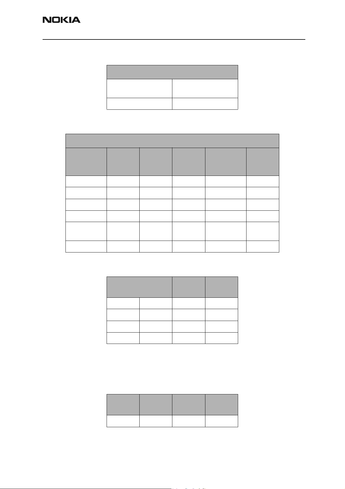
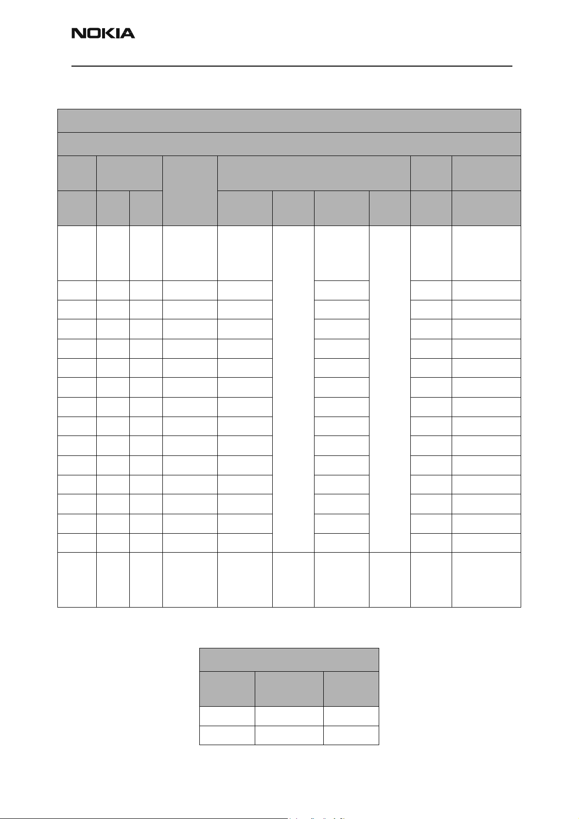
Cell Transmitter
Cell Transmitter Path
The following table indicates the test points to probe when troubleshooting the cell
transmitter path. The steps shown are the recommended but do not have to be followed
in that order. Refer to the Appendix for a reference diagram that illustrates the test
points on the circuit board. An HP high frequency probe is used to make the frequency
and output power measurements.
Constant Reference
Values
CELL Oscillator and IF:
VHF Tx Lo
457.2
VHF Rx Lo
367.2
Setup:
Mode
Local On On PCS/CELL CDMA GenIO 8 = H TxIF and RF
Tx Rx Band
Chnn Tx Freq Rx Freq UHF GenIO 12 = L
384 836.52 881.52 1065.12 GenIO 13 = L
600 1880 1960 2143.6
Tx IF
228.6
Rx IF
183.6
CW or
CDMA
BB GenIO PDM Rho
AGC = 0
On
Issue 1 06/2003 Nokia Corporation Confidential Page 7
Page 8
RH-3
Troubleshooting - RF CCS Technical Documentation
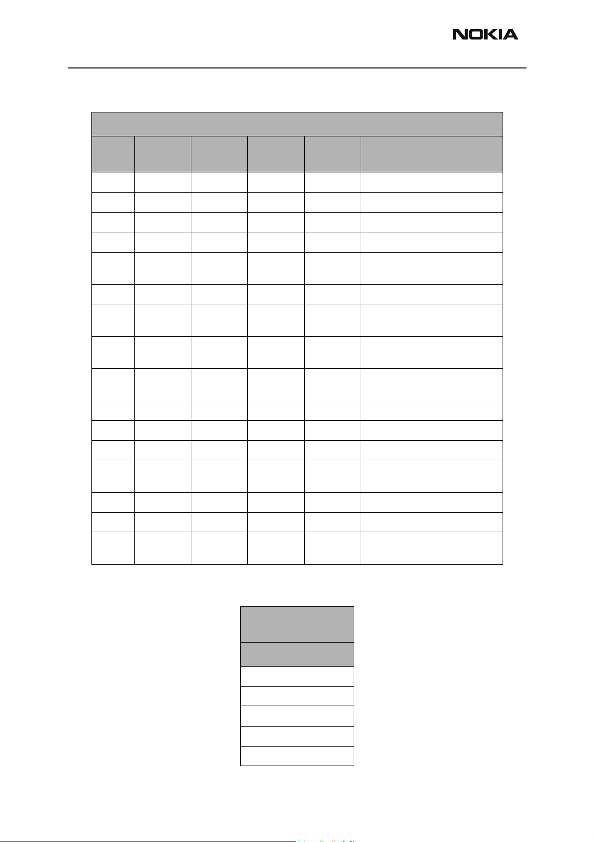
Step # Part Part Ref Label Test Point
1 Jedi Pin 7 I+ J601 0.1 to 0.9,
2 Jedi Pin 8 I- J602 0.1 to 0.9,
3 Jedi Pin 4 Q+ J603 0.1 to 0.9,
4 Jedi Pin 5 Q- J604 0.1 to 0.9,
5 Jedi Pin 45 IF CELL- top-C603 -45, 228.6 dBm/30kHz,
6 Jedi Pin 46 IF CELL+ bottom-C603 -45, 228.6 dBm/30kHz,
7 Jedi Pin 31 CELL_DRVout pin 1-Z601 -38 dBm/30kHz
8 Z601 Pin 3 SAW out pin 3 -40 dBm/30kHz
9 Orca Pin 2 RF in pin 3-Z601 -40 dBm/30kHz
10 Orca Pin 8 PA out left-R814 -17.5 dBm/30kHz
Typical
Value
1.7
1.8
1.9
1.10
Units Comments
VAC, VDC Test Point on
VAC, VDC
VAC, VDC
VAC, VDC
MHz
MHz
BB side
11 Z802 Pin 1 Iso Out=Dup Inpin 11-Z803 dBm/30kHz This test point
is inaccessible
12 Z803 Pin 8 Dup-Ant pin 8 -19 dBm/30kHz This point is
only accessible if the CELL
duplexer can
shield is
removed
13 Z800 Pin 3 Diplexer left-L802 -19
Cell Power Amplifier
The table above is the path that one would take to determine where the problem is in the
transmitter path. There are other circuits that affect the operation of the transmitter
path; for example, the power amplifier (PA) has the DC/DC converter (PMIC device)
which controls it. The following tables illustrate the circuits that have an effect on the
transmitter path and how to troubleshoot them.
The following table illustrates the PA troubleshooting information.
Page 8 Nokia Corporation Confidential Issue 1 06/2003
Page 9
RH-3
CCS Technical Documentation Troubleshooting - RF
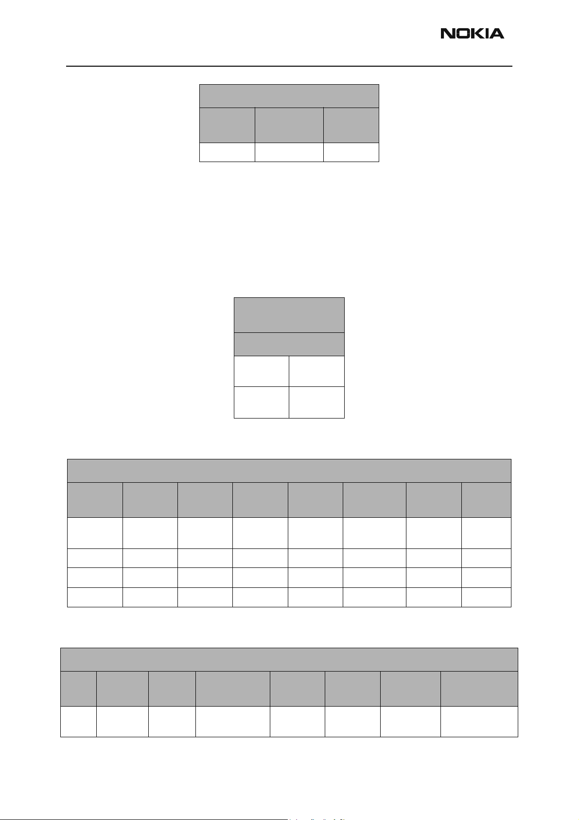
PA Power and Gain Measurements
Power Amplifier Input
Test Point
pin3-Z601 right-R814
PA Power and Gain Specifications
Power
Mode Name
Gain mode 0 V0 up to 9 23.8 0.75- 0.88 C806
Gain mode 1 V1 9 to 13 25.2 1.125- 1.375 C806
Gain mode 3 V2 Not used Not used 2 - 2.5 C806
Gain mode 2 Bypass 13 up 29 3 - 4 C806
Overall Gain V0 to
Bypass
unit N/A dBm dB VDC N/A
Output
Range
9 3.5 to 7.3
Power Amplifier Output
Test Point
Nominal
Gain
+/- 0.5
Vcc Range
Vcc Test
Point
* Depends on VBATT
Cell PMIC
The following table illustrates the PMIC troubleshooting information.
PA Gain Step
Gen IO 12 GenIO13
LL0.8V0
HL 1.2V1
LH2.2V2
HH3.7Bypass
Setup:
Mode
Local On On PCS/CELL
Tx Rx Band
PA Vcc
volt (v)
Spec
Name
Issue 1 06/2003 Nokia Corporation Confidential Page 9
Page 10
RH-3
Troubleshooting - RF CCS Technical Documentation
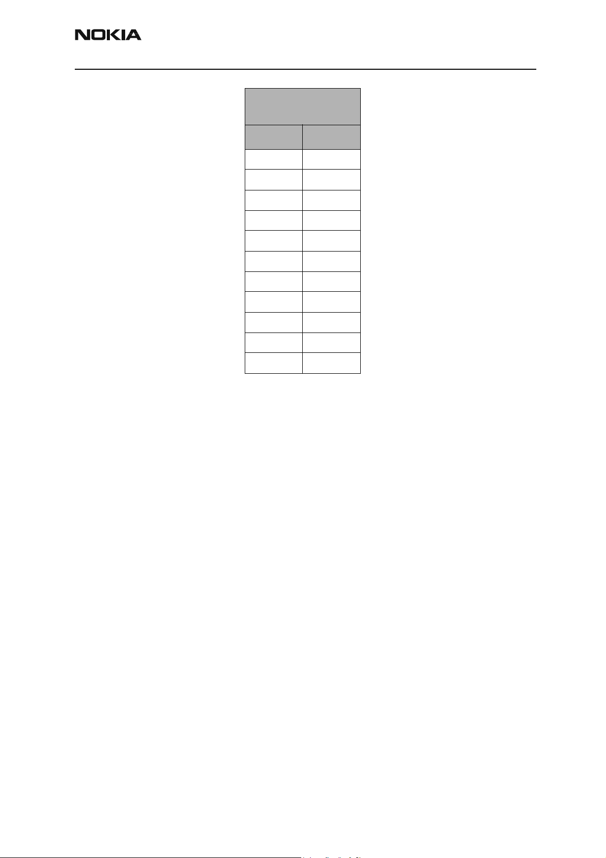
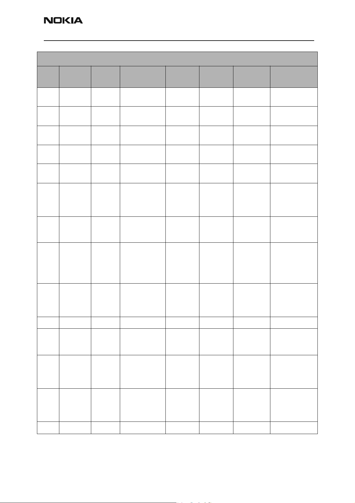
Measurements:
Pin Label Test Point Units
1 EP Pin 1 1.8 UPP IC enable = GenIO 10
2 M0 Pin 2 1.8 UPP Control 0 = GenIO 12
3 M1 Pin 3 1.8 UPP Control 1 = GenIO 13
4NCNCNCNCNC
5 FB Pin 5 0.75 - 4 M0, M1 See PA worksheet. Output to fly-
6 FB Pin 6 0.75 - 4 M0, M1 Shares PWB pad with pin 5
7 BYPVout bottom-
C808
8 VDD right-L810 VBATT VBATT Digital DC supply, shared with
9 VSS GND GND GND Digital GND, shared gnd with pin
10 NC NC NC NC NC
11 Vbgap NC NC NC Bandgap voltage output
0.75 - 4 M0, M1 PMIC bypass output used at Pout
Depends
on
Comments
back inductor
> 12 dBm
pin 12, 14, 15
13
12 VDD right-L810 VBATT VBATT Digital DC supply
13 Vss GND GND GND Digital GND, shared gnd with pin
9
14 Vsw right-L810 VBATT VBATT Switcher supply
15 Vsw right-L810 VBATT VBATT Switcher supply
16 Gsw GND GND GND Switcher GND, does not share
with pin 9 and pin 13
Good phone PMIC
Resistances
Pin Resistance
160k
275k
380k
41.59M
51.6M
Page 10 Nokia Corporation Confidential Issue 1 06/2003
Page 11
RH-3
CCS Technical Documentation Troubleshooting - RF
Good phone PMIC
Resistances
Pin Resistance
62M
72M
82M
90.1
10 100
11 115 k
12 60k
13 0.2
14 1.3M
Cell IF and RF AGC and PA Control
The following table illustrates the PDM values and their typical values for the IF AGC, RF
AGC Jedi Pout, Gain steps, and the PA VCC levels. It also shows the typical power output
at the RF connector.
15 1.18M
16 0.1
Issue 1 06/2003 Nokia Corporation Confidential Page 11
Page 12
RH-3
Troubleshooting - RF CCS Technical Documentation
.
Cell CDMA Chnn 384
TX RF AGC TX IF AGC Jedi Po
PA Gain
Step
PA Vcc
Con
Typi
PDM
cal
Valu
Test
Point
PDM
e
-324 0.41 Bottom
C606
-226 0.56 -226 0.56 -21 H H 3.61 28 20
-146 0.68 -146 0.68 -21 H H 3.67 28 15.1
-146 0.68 -146 0.68 -27 H L 1.2 26 13
-111 0.74 -111 0.74 -28 H L 1.2 25.8 10.3
-111 0.74 -111 0.74 -28 L L 0.82 24.5 9
-6 0.9 -6 0.9 -35 L L 0.82 0
52 1 52 1 -45 L L 0.82 -10
105 1.09 105 1.09 -54 L L 0.82 -20
180 1.09 180 1.21 -64 L L 0.82 -30
266 1.36 266 1.36 -74 L L 0.82 -40
-324 0.41 Top
Typi
cal
Valu
e
Test
Point
C605
Typi
cal
Valu
Test
Point
e
-17 pin 1
Z601
Gen
IO
13
Typi
cal
Valu
e
Test
Point
PA
Gain
Gen
IO
12
H H 3.47 C806 DM 25
n RF
Pout
353 1.5 353 1.49 -83 L L 0.82 -50
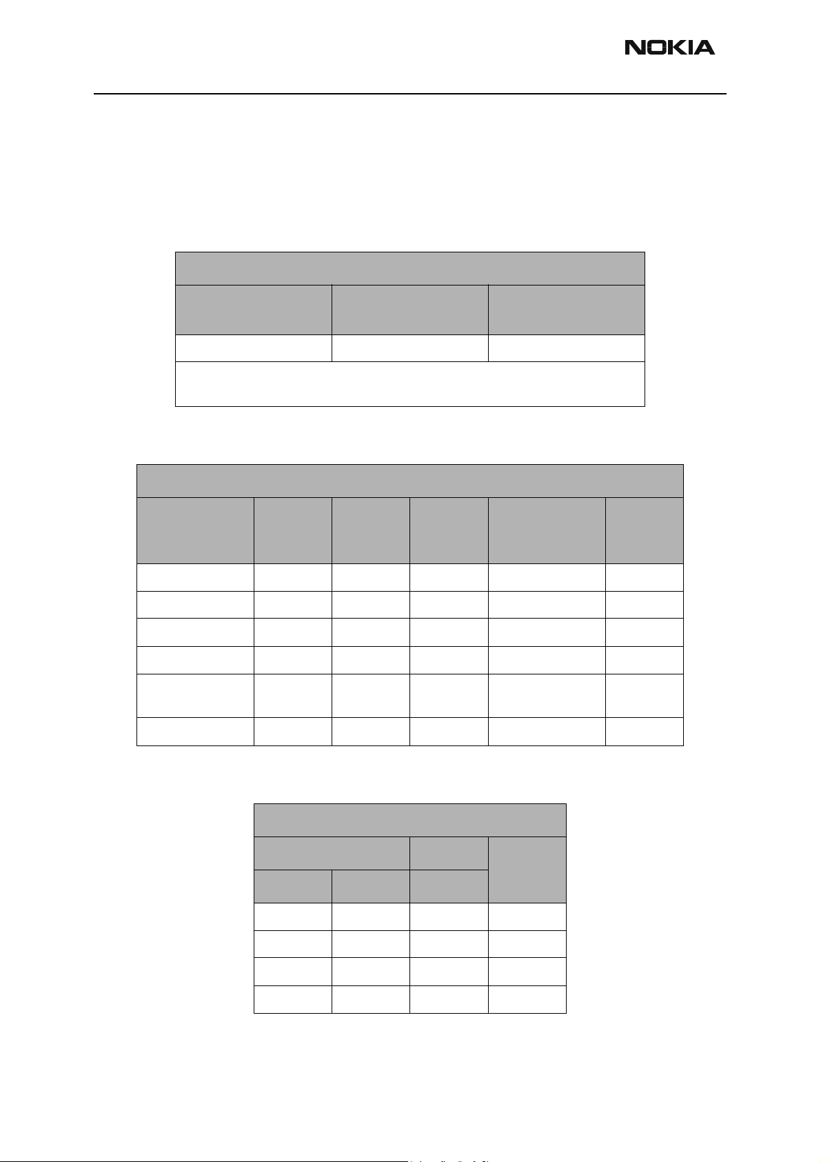
Cell Power Detector
The following tables illustrate the measurements required for troubleshooting the Cell
power detector.
Setup:
Mode Tx Rx Band Chnn Rho
Local On On PCS/CELL 600/384 On
Input Chnn Tx Freq Rx Freq
384 836.52 881.52
600 1880 1960
Page 12 Nokia Corporation Confidential Issue 1 06/2003
Page 13
RH-3
CCS Technical Documentation Troubleshooting - RF
Measurements:
CELL, Channel 384
TX
ADC
RF/IF
pdm
353 L L -50 -86.3 right
140 L L -25 -63 2 235
-5 L L 0 -41 1.998 235
-105 L L 9 -30 1.967 250
-105 H L 10 -29 1.957 268
-143 H L 13 -26 1.93 286
-143 H H 14.9 -23.5 1.9 435
-175 H H 17 -21.5 1.86 486
-210 H H 19 -19 1.812 550
-246 H H 21 -17 1.745 630
PA Gain Step
GIO 12GIO
13
Conn RF
Pout
Power Detector Comments
Pout at
detector
Test
Point
R814
Det Out
2left
Test
Point
C807
mA
235 CELL band and
Det=Detector
Po=Power
detector coupling is about
22 dB
-286 H H 23 -15 1.667 730
-330 H H 25 -12 1.547 860
-352 H H 26 -11.5 1.485 950
-365 H H 26.5 -11 1.44 1000
-387 H H 27.5 -10 1.36 1095
none dBm dBm/
30kHz
Detector Reference and DC Supply
Label Test Point
Det Ref left-C803 2
Det Supply bottom-C257 2.8
VDC dBm only
Typical
Value
refers to total
power measured
Issue 1 06/2003 Nokia Corporation Confidential Page 13
Page 14
RH-3
Troubleshooting - RF CCS Technical Documentation
Detector Reference and DC Supply
PCS Transmitter
PCS Transmitter Path
The following table indicates the test points to probe when troubleshooting the PCS
transmitter path. The steps shown are the recommended but do not have to be followed
in order. Refer to the Appendix for a reference diagram that illustrates the test points on
the circuit board. An HP high-frequency probe is used to make the frequency and output
power measurements.
Label Test Point
Constant Reference
Values
PCS Oscillator and IF:
VHF Tx Lo
527.2
VHF Rx Lo
367.2
Typical
Value
VDC
Tx IF
263.6
Rx IF
183.6
Setup:
Mode Tx Rx Band
Local On On PCS/CELL CDMA GenIO 8 = H Tx IF and
Chnn Tx Freq Rx Freq UHF GenIO 12 = L
384 836.52 881.52 1065.12 GenIO 13 = L
600 1880 1960 2143.6
PCS TX
Step
#
1 Jedi Pin 7 I+ J601 0.1 to 0.9,
Part Part Ref Label Test Point
CW or
CDMA
BB GenIO PDM Rho
RF AGC = 0
Typical
Value
1.7
Units Comments
VAC, VDC
On
Page 14 Nokia Corporation Confidential Issue 1 06/2003
Page 15
RH-3
CCS Technical Documentation Troubleshooting - RF
PCS TX
Step
#
2 Jedi Pin 8 I- J602 0.1 to 0.9,
3 Jedi Pin 4 Q+ J603 0.1 to 0.9,
4 Jedi Pin 5 Q- J604 0.1 to 0.9,
5 Jedi Pin 45 If PCS- top C604 -44, 263.6 dBm/30kHz,
6 Jedi Pin 46 IF PCS+ bottom
7 Jedi Pin 31 PCS_DRVout_A bottom
8 Jedi Pin 31 PCS_DRVout_B right L605 -30, 1880 dBm/30kHz,
Part Part Ref Label Test Point
C605
L604
Typical
Value
1.8
1.9
1.10
-44, 263.6 dBm/30kHz,
-51, 1880 dBm/30kHz,
Units Comments
VAC, VDC
VAC, VDC
VAC, VDC
MHz
MHz
MHz
MHz
A output is for
chnns 25 to 599.
This measured
power is leakage.
B output is for
channs 600 to
11 75
9 Z602 Pin 1 SAW out A pin3 N602 -56 dBm/30kHz The outputs of
Z602 and the
inputs to N602
are difficult to
reach
10 Z602 Pin 3 SAW out B pin 1 N602 -32 dBM/30kHz If not necessary,
skip to the PA
input measurement
11 Shamu Pin 4 RF in left C640 -32 dBm/30kHz
12 Shamu Pin 8 PA out left R803 -9 dBm/30kHz Accessible only if
Isolator shield
can is removed
13 Z801 Pin 6 Iso Out=Dup In none none dBm/30kHz Accessible only if
PCS duplexor
shield can is
removed
14 Z804 Pin Rx ant none none dBm/30kHz Accessible only if
PCS duplexor
shield can is
removed
15 Z800 P3 Diplexer left L802 -14 dBm/30kHz
PCS Power Amplifier
The preceding table is the path that one would take to determine where the problem is in
Issue 1 06/2003 Nokia Corporation Confidential Page 15
Page 16
RH-3
Troubleshooting - RF CCS Technical Documentation
the transmitter path. There are other circuits that affect the operation of the transmitter
path; for example, the power amplifier (PA) has the DC/DC converter (PMIC device) that
controls it. The following tables illustrate the circuits that have an affect on the transmitter path and how to troubleshoot them.
The table below illustrates the PA troubleshooting information.
PA Power and Gain Measurements
Power Amplifier Input
Test Point
right C640 * left R803 ** right C804
* inaccessible unless shield can is removed (no lid)
** This is the coupled power. You must 30 dB to get correct value
PCS PA Power and Gain Specifications
Mode Name
Gain mode 0 V0 up to 8 22.4 0.75 - 0.88 C806
Gain mode 1 V1 8 to 12 24.4 1.125 - 1.375 C806
Gain mode 3 V2 Not Used Not Used 2 - 2.5 C806
Gain mode 2 Bypass 12 up 28 3 - 4 C806
Overall gain VO to
bypass
Power Amplifier Output
Test Point 1
Power
Output
Range
8 3.6 to 7.6
Nominal
Gain
+/- 0.5
Power Amplifier Output
Test Point 2
Vcc Range
Vcc Test
Point
unit dBm dB VDC N/A
Phoenix Control and Example Values
PA Gain Step PA Vcc
GenIO 12 GenIO 13 volt (v)
LL0.8V0
HL 1.2V1
LH2.2V2
HH3.7Bypass
Spec
Name
Page 16 Nokia Corporation Confidential Issue 1 06/2003
Page 17
RH-3
CCS Technical Documentation Troubleshooting - RF
PCS PMIC
The following table illustrates the PMIC troubleshooting information.
Setup:
Mode Tx Rx Band
Local On On PCS/CELL
Measurements:
Pin Label Test Point Units
1 EP Pin 1 1.8 UPP IC enable = GenIO 10
2 M0 Pin 2 1.8 UPP Control 0 = GenIO 12
3 M1 Pin 3 1.8 UPP Control 1 = GenIO 13
4NCNCNCNCNC
5 FB Pin 5 0.75 - 4 M0, M1 See PA worksheet. Output to fly-
6 FB Pin 6 0.75 - 4 M0, M1 Shares PWB pad with pin 5
7 BYPVout bottom
C808
8VDD right
L810
9 VSS GND GND GND Digital GND, shared gnd with pin
10 NC NC NC NC NC
11 Vbgap NC NC NC Bandgap voltage output
0.75 - 4 M0, M1 PMIC bypass output used at Pout
VBATT VBATT Digital DC supply, shared with
Depends
on
Comment
back inductor
> 12 dBm
pin 12, 14, 15
13
12 VDD right
L810
13 Vss GND GND GND Digital GND, shared gnd with pin
14 Vsw right
L810
15 Vsw right
L810
16 Gsw GND GND GND Switcher GND, does not share
VBATT VBATT Digital DC supply
9
VBATT VBATT Switcher supply
VBATT VBATT Switcher supply
with pin 9 and pin 13
Issue 1 06/2003 Nokia Corporation Confidential Page 17
Page 18

RH-3
Troubleshooting - RF CCS Technical Documentation
Good phone PMIC
Resistances
Pin Resistance
160k
275k
380k
41.59M
51.6M
62M
72M
82M
PCS IF and RF AGC and PA Control
The following table illustrates the PDM values and their typical values for the IF AGC, RF
AGC Jedi Pout, Gain steps, and the PA VCC levels. It also shows the typical power output
at the RF connector.
90.1
10 100
11 115 k
12 60k
13 0.2
14 1.3M
15 1.18M
16 0.1
Page 18 Nokia Corporation Confidential Issue 1 06/2003
Page 19

RH-3
CCS Technical Documentation Troubleshooting - RF
PCS CDMA Chnn 600
TX RF AGC TX IF AGC Jedi Po
PA Gain
Step
PA Vcc
Con
Typi
PDM
cal
Valu
Test
Point
PDM
e
-133 0.71 Bottom
C606
-96 0.77 -96 0.77 -19 H H 3.65 30 20
-52 0.83 -52 0.83 -25 H H 3.65 30 16.3
-52 0.83 -52 0.83 -25 H L 1.2 26 12
-31 0.86 -31 0.86 -28 H L 1.2 26 10.3
-31 0.86 -31 0.86 -28 L L 0.81 25 8
39 0.98 39 0.98 -36 L L 0.81 25 0
91 1.07 91 1.07 -46 L L 0.82 25 -10
159 1.18 159 1.18 -58 L L 0.82 27 -20
244 1.32 244 1.32 -69 L L 0.82 25 -30
331 1.46 331 1.46 -80 L L 0.82 25 -40
-133 0.71 Top
Typi
cal
Valu
e
Test
Point
C605
Typi
cal
Valu
Test
Point
e
-17 right
L605
Gen
IO
13
Typi
cal
Valu
e
Test
Point
PA
Gain
Gen
IO
12
H H 3.55 C806 DM 23
n RF
Pout
418 1.6 418 1.6 -89 L L 0.82 25 -50
PCS Power Detector
The following tables illustrate the measurements required for troubleshooting the PCS
power detector.
Setup:
Mode Tx Rx Band Chnn Rho
Local On On PCS/CELL 600/384 On
Input Tx Freq Rx Freq
384 836.52 881.52
600 1880 1960
Issue 1 06/2003 Nokia Corporation Confidential Page 19
Page 20

RH-3
Troubleshooting - RF CCS Technical Documentation
PCS, Chnn 600
TX AGC
RF/IF pdm
418 L L -50 -87 right R814 2 left C807 250 PCS band
201 L L -25 -68 right R814 2 left C807 250
39 L L 0 -41.5 right R814 2 left C807 255 RF amplifier
-30 L L 8 -33 right R814 1.986 left C807 263
-30 H L 10.2 -31 right R814 1.984 left C807 278
-51 H L 12 -29 right R814 1.979 left C807 285
-72 H H 18 -21.5 right R814 1.93 left C807 473
PA Gain
Step
GIO 12GIO
13
Conn
RF
Pout
Pout at
Detector
Power Detector Comments
**Det =
Detector
Po = Power
detector coupling is about
30 dB
has the most
gain increase
near 0 dBm
Test Point
Det
Out
Test Point mA
-85 H H 19 -21 right R814 1.914 left C807 500
-108 H H 21 -19 right R814 1.882 left C807 557
-133 H H 23 -17 right R814 1.84 left C807 634
-148 H H 24 -16.5 right R814 1.81 left C807 685
-162 H H 25 -16 right R814 1.778 left C807 740
Detector Reference and DC Supply
Label Test Point Typical Value
Det Ref left C803 2
Det Supply bottom C257 2.8
VDC
Page 20 Nokia Corporation Confidential Issue 1 06/2003
Page 21

RH-3
CCS Technical Documentation Troubleshooting - RF
Receiver Troubleshooting
Cell Receiver
Receiver Path (Cell mode)
Setup:
Input power -50 dBm
Input Freq 881.52 MHz
Rx AGC PDM 225 PDM
CDMA Generator Code Domain Setup
Channel Power
Pilot -7 dB 0
Paging -12 dB 1
Traffic -15.6 dB 10
Sync -16 dB 32
Measurements
Step Part Part Ref Label Test Point
1 Diplexer none RF Conn Diplexer
Pin 3
2 Alfred Pin 11 CELL LNA
input
3 Alfred Pin 13 CELL LNA
output
Alfred Pin 11-68 dBm/30kHz expected LNA gain
bottom
L901
Walsh
code
Typical
Value
*-73 dBm/30kHz
-59 dBm/30kHz Yoda register 6.
Units Comments
= 12 to 14 dB
Defaults to high
gain mode
4 Alfred Pin 16 CELL Mixer
input
5 Alfred Pin 17 Mixer out-
put (183.6
MHz)
Alfred Pin 16-53 dBm/30kHz Note that this is a
passive device but
impedances cause
power level to
appear higher
right L903 -54 dBm/30kHz Mixer is passive
and typical conversion gain is -5
dB
Issue 1 06/2003 Nokia Corporation Confidential Page 21
Page 22

RH-3
Troubleshooting - RF CCS Technical Documentation
Measurements
Step Part Part Ref Label Test Point
6 Alfred Pin 18 IF Amp
input
7 Alfred Pin 22 IF output
(565 ohms)
8 Z701 Pin 5 IF filter
input
9 Yoda Pin 31 VGA input 1right C702 -56 dBm/30kHz see TS picts 2, doc
10 Yoda Pin 32 VGA input 2right C707 -56 dBm/30kHz both look same
11 Yoda Pin 8 Qb out J704 0 to 0.6,
12 Yoda Pin 7 Q out J703 0 to 0.6,
right C906 -56 dBm/30kHz
left L909 -33 dBm/30kHz IF amp gain typi-
top L702 -42 dBm/30kHz impedance change
Typical
Value
1.3
1.3
Units Comments
cally 15 to 19
creates -10 dB
delta
#2
and look distorted
VAC, VDC see TS picts 2.doc
#3,4,5 SA view of
BB I or Q
VAC, VDC see TS picts 2.doc
#3,4,5 SA view of
BB I or Q
13 Yoda Pin 8 lb out J702 0 to 0.6,
1.3
14 Yoda Pin 9 1 out J701 0 to 0.6,
1.3
Alfred (Cell mode)
Constant Reference Values:
CELL Iscillator and IF
VHF Tx Lo
457.2
VHF RX Lo
367.2
Setup
Tx IF
228.6
Rx IF
183.6
VAC, VDC see TS picts 2.doc
#3,4,5 SA view of
BB I or Q
VAC, VDC see TS picts 2.doc
#3,4,5 SA view of
BB I or Q
Mode Tx Rx Band
Local Off On PCS/CELL CW -80 dBm RX IF AGC
CW or
CDMA
Pin
Default
PDM
= 0
LNA Gain
Mode
High
Page 22 Nokia Corporation Confidential Issue 1 06/2003
Page 23

RH-3
CCS Technical Documentation Troubleshooting - RF
Setup
Mode Tx Rx Band
Input Chnn Tx Freq Rx Freq UHF
384 836.52 881.52 1065.12
600 1880 1960 2143.6
Measurements
CELL
Pin Label Test Point
1 LO_VDD_P bottom
L908
2 LO_VDD_C top L908 2.3, -15,
Typical
Value
2.63, 13.4,
1065.12
1065.12
CW or
CDMA
PCS
Typical
Value
2.48, -15.6,
2143.6
2.45, 11,
2143.6
Pin
Units
VDC, dBm,
MHz
VDC, dBm,
MHz
Default
PDM
Depends
on
VR4, band Only an inductor
VR4, band measured is off-
LNA Gain
Mode
Comments
separates pin 1
and 2
set by the LO
power
3 BAND left C911 Q 2.63 VDC Yoda
4 P_MIX_IN left L911 NA -72, 1960 dBm, MHz band PCS band
5 P_RFA_VDDtop R910 2.7 2.7 VDC VR4 PCA band
6 GND NA NA NA NA NA
7 GAIN_CTL left C909 2.7 2.7 VDC Yoda LNA gain switch
8P_LNA_OUTbottom
C902
9 GND NA NA NA NA NA
10 P_LNA_IN Pin 10 NA -83, 1960 dBm band PCS band
11 C _ L N A _IN Pin 11 -8 0 ,
12GNDNANANANANA
13 C_LNA_OUTbottom
L901
14 VDD top R910 2.7 2.7 VDC VR4 closer MPs are
NA -69, 1960 dBm, MHz band PCS band
NA dBm, MHz band CELL band
881.52
-69,
881.52
NA dBm, MHz band CELL band
blocked by shield
15 RFA_VDD_Ctop R910 2.7 2.7 VDC VR4 same as pin 5
16 C_MIX_IN Pin 16 -75,
881.52
NA dBm, MHz band CELL band
Issue 1 06/2003 Nokia Corporation Confidential Page 23
Page 24

RH-3
Troubleshooting - RF CCS Technical Documentation
Measurements
CELL
Pin Label Test Point
17 MIX_OUT right L903 -66, 183.6 -67, 183.6 dBm, MHz UHF LO UHF = 1055.12
18 IFA_IN right C905 -63, 183.6 -65, 183.6 dBm, MHz
19 IFA_SRC right L910 -63, 183.6 -65, 183.6 dBm, MHz
20 AMPS_OUT NC NC NC NC NC No AMPS in this
21GNDNANANANANA
22 CDMA_OUTleft L909 -42, 183.6 -44 dBm, MHz Alfred provides
23 IF_SEL Pin 23 0 0 VDC Always gnded for
24 LQ_IN top L 904 1, 1065.12 2.4, 2143.6 dBm, MHz UHF LO
Typical
Value
PCS
Typical
Value
Units
Depends
on
Comments
(CELL), 2143.6
(PCS)
application
about 40 dBm of
overall
this frequency
plan
Yoda (Cell mode)
Constant Reference Values
Cell Oscillator and IF
VHF Tx Lo
457.2
VHF Rx Lo
367.2
Setup
Mode Tx Rx Band
Local Off On PCS/CELL CW -80dBm RX IF AGC
Input Chnn Tx Freq Rx Freq UHF
Tx IF
228.6
Rx IF
183.6
CW or
CDMA
Pin
Default
PDM
= 0
LNA Gain
Mode
High
384 836.52 881.52 1065.12
600 1880 1960 2143.6
Page 24 Nokia Corporation Confidential Issue 1 06/2003
Page 25

RH-3
CCS Technical Documentation Troubleshooting - RF
Measurements
CELL
Pin Label Test Point
1 AGC_CON right C703 0.916 0.916 VDC UPP RX_IF_AGC =
2 AGC_REF right C725 1.8 1.8 VDC VIO PDM = 0
3 VREF right C731 1.36 1.36 VDC UEM pin
4 RBIAS right R706 1.21 1.2 VDC UEM sets internal bias
5 AVDD_RX right C742 2.8 2.8 VDC VR6 analog DC supply
6 Qb J704 1.25, 0.2 1.25, 0.2 VDC, VAC
7 Q J703 1.25, 0.2 1.25, 0.2 VDC, VAC
8 lb J702 1.25, 0.2 1.25, 0.2 VDC, VAC
9 l J701 1.25, 0.2 1.25, 0.2 VDC, VAC
10 OFFI right C735 1.65 1.65 VDC I signal DAC. Off-
Typical
Value
PCS
Typical
Value
Units
Depends
on
H13
Comments
GenIO 09, Equals
0.918 VDC when 0
same as
RF_CONV0(9) at
UEM
current
set high freq tx
11 OFFQ left C736 1.65 1.65 VDC Q signal DAC. Off-
set high freq tx
12 CLK BB J450 2.2, 9.6 2.2.9.6 VAC, MHz UPP RF_CLK = VCTCXO
2 bursts
13 DATA BB J451 2.2 2.2 VAC UPP Digital control
data for Yoda
14 LE BB J452 2.2 2.2 VAC UPP Enable pin for
Yoda
15 DVDD right C710 1.8 1.8 VDC VIO Digital DC supply
16 19.2OUT/
LD(1.8)
17 AVDD_TCXOleft C734 2.8 2.8 VDC VR3 VCTCXO buffer
18 TCXO_IN right C728 5, 19.2 5, 19.2 dBm, MHz VCTCXO VCTCXO input to
19 DVDD_SYNTHleft C704 1.8 1.8 VDC VIO Digital Yoda syn-
right C711 5, 19.2 5, 19.2 dBm, MHz VCTCXO Amplified output
of DC TCXO
amplifier DC supply
Yoda
thesizer DC supply
Issue 1 06/2003 Nokia Corporation Confidential Page 25
Page 26

RH-3
Troubleshooting - RF CCS Technical Documentation
Measurements
CELL
Pin Label Test Point
20 AVSS_SYNTHGND GND GND GND GND GND
21 AVDD_SYNTHleft R703 2.75 2.75 VDC VR7 Analog Yoda syn-
22 CP right C754 -7.5, 367.2 -7,367.2 dBm, MHz Charge pump out-
23 VCO_TANKbleft C754 1,367.2 1,367.2 dBm, MHz pin 22, VR7 VCO external var-
24 AVDD_VCO2bottom
C720
25 OUT4_CTR
L_TEST_1b
26 OUT3_CTR
L_TEST_1
27 OUT2_CTR
L_TEST_Qb
NC NC NC NC NC NC
Pin 7(TL) 2.7 0 VDC G501 synthesizer
bottom
R904
Typical
Value
2.7 2.7 VDC VR7 Analog VCO DC
0 2.7 VDC Alfred RF band
PCS
Typical
Value
Units
Depends
on
Comments
thesizer DC supply
put
actor control
supply
band select
select
28 OUT1_CTR
L_TEST_Q
29 AVDD_MIX bottom
30 AVDD_if bottom
31 VGA_IN right C707 -70, 183.6 -73, 183.6 dBm, MHz Alfred out-
32 VGA_INB right C702 -70, 183.6 -73, 183.6 dBm, MHz Alfred out-
bottom
R902
C712
C744
27.0 27.0 VDC-H,
VDC-L
2.7 2.7 VDC VR6 Mixer analog DC
2.7 2.7 VDC VR6 Mixer analog DC
put
put
Alfred LNA gain
state control
voltage supply
voltage supply
Yoda RF input A
from Alfred
Yoda RF input B
from Alfred
Page 26 Nokia Corporation Confidential Issue 1 06/2003
Page 27

RH-3
CCS Technical Documentation Troubleshooting - RF
RX AGC (Cell mode)
RX RF AGC PDM vs AGC Voltage
RX RF AGC
PDM
-512 0.1 right C703
-400 0.279
-300 0.436
-200 0.597
-100 0.753
00.913
100 1.076
200 1.24
300 1.403
350 1.484
400 1.565
500 1.727
511 1.745
Typical
Value
Test Point Comments
UNITS VDC
Rx AGC vs RF Pin for CELL and PCS
Bands
Conn RF
Pin
-25 1.485 1.512
-35 1.298 1.336
-45 1.159 1.18 In Normal mode, the phone will adjust RF RX
-55 1.019 1.039 Rx power is coming in, the I and Q will be about
-65 0.861 0.896
-75 0.728 0.747 Approximately 1 pdm per 1 mV
-85 0.563 0.596
CELL
RF AGC
PCS
RF AGC
Comments
AGC
0.5 Vpp and 1.3 V
Issue 1 06/2003 Nokia Corporation Confidential Page 27
Page 28

RH-3
Troubleshooting - RF CCS Technical Documentation
Rx AGC vs RF Pin for CELL and PCS
Bands
Conn RF
Pin
-94 0.441 0.46
-95 0.431 0.66 Note the reduced delta because the LNA is
-96 0.651 0.646 LNA switch hysteresis: -94 on the way down,
-100 0.594 0.59
-105 0.524 0.59
-107 0.493 0.485
UNITS VDC VDC
CELL
RF AGC
PCS Receiver
Receiver Path (PCS mode)
PCS
RF AGC
PCS CDMA Rx Test
Setup:
Comments
switched on
-89 on the way up
Input power: -50 dBm
Input Freq: 1960 MHz
Rx AGC PDM: 225 PDM
CDMA Generator Code Domain Setup
Channel Power Walsh code
Pilot -7 dB 0
Paging -12 dB 1
Traffic -15.6 dB 10
Sync -16 dB 32
Page 28 Nokia Corporation Confidential Issue 1 06/2003
Page 29

RH-3
CCS Technical Documentation Troubleshooting - RF
Measurements
Step Part Part Ref Label Test Point Typical Value Units
1 Diplexer none RF Conn Diplexer Pin 1 -67 dBm/30kHz
2 Alfred Pin 10 PCS LNA input Alfred Pin 10 -70 dBm/30kHz
3 Alfred Pin 8 PCS LNA output bottom C902 -57 dBm/30kHz
4 Alfred Pin 4 PCS Mixer input left C911 -59 dBm/30kHz
5 Alfred Pin 17 Mixer output
(183.6 MHz)
6 Alfred Pin 18 IF AMP input right C906 -50 dBm/30kHz
7 Alfred Pin 22 IF output (565
ohms)
8 Z701 Pin 5 IF filter input top L702 -39 dBm/30kHz
9 Yoda Pin 31 VGA input 1 right C702 -56 dBm/30kHz
10 Yoda Pin 32 VGA input 2 right C707 -58 dBm/30kHz
11 Yoda Pin 6 Qb out J704 0 to 0.6, 1.3 VAC, VDC
12 Yoda Pin 7 Q out J703 0 to 0.6, 1.3 VAC, VDC
13 Yoda Pin 8 lb out J702 0 to 0.6, 1.3 VAC, VDC
14 Yoda Pin 9 l out J701 0 to 0.6, 1.3 VAC, VDC
right L903 -53 dBm/30kHz
left L909 -31 dBm/30kHz
Alfred (PCS mode)
Constant Reference Value
PCS Oscillator and IF:
VHF TxLo
527.2
VHF Rx Lo
367.2
Setup:
Mode Tx Rx Band
Local Off On PCS/CELL CW -80 dBm RX IF AGC
Input Chnn Tx Freq Rx Freq UHF
Tx IF
263.6
Rx IF
183.6
CW or
CDMA
Pin
Default
PDM
= 0
LNA Gain
Mode
High
Issue 1 06/2003 Nokia Corporation Confidential Page 29
Page 30

RH-3
Troubleshooting - RF CCS Technical Documentation
Setup:
Mode Tx Rx Band
384 836.52 881.52 1065.12
600 1880 1960 2143.6
Measurements
CELL
Pin Label Test Point
1 LO_VDD_P bottom L908 2.63, 13.4,
2 LO_VDD_C top L908 2.3, -15,
3 BAND left C911 0 2.63 VDC Yoda
4 P_MIX_IN left L911 NA -72, 1960 dBm, MHz band PCS band
Typical
Value
1065.12
1065.12
CW or
CDMA
PCS
Typical
Value
2.48, -15.6,
2143.6
2.45, 11,
2143.6
Pin
Units
VDC, dBm,
MHz
VDC, dBm,
MHz
Default
PDM
Depends
on
VR4, band Only an inductor
VR4, band measured is off-
LNA Gain
Mode
Comments
separates pin 1
and 2
set by LO power
5 P_RFA_VDD top R910 2.7 2.7 VDC VR4 PCS band
6 GND NA NA NA NA NA
7 GAIN_CTL left C909 2.7 2.7 VDC Yoda LNA gain switch
8 P_LNA_OUT bottom C902 NA -69, 1960 dBm, MHz band PCS band
9 GND NA NA NA NA NA
10 P_LNA_IN Pin 10 NA -83, 1960 dBm band PCS band
11 C _ L N A_ I N Pin 11 - 8 0 ,
881.52
12GND NA NANANANA
13 C_LNA_OUT bottom L901 -69,
881.52
14 VDD top R910 2.7 2.7 VDC VR4 closer MPs are
15 RFA_VDD_C top R910 2.7 2.7 VDC VR4 same as pin 5
16 C_MIX_IN Pin 16 -75,
881.52
17 MIX_OUT right R903 -66, 183.6 -67, 183.6 dBm, MHz UHF LO UHF = 1065.2
NA dBm, MHz band CELL band
NA dBm, MHz band CELL band
blocked by shield
NA dBm, MHz band CELL band
(CELL), 2143.6
(PCS)
18 IFA_IN right C906 -63, 183.6 -65, 183.6 dBm, MHz
Page 30 Nokia Corporation Confidential Issue 1 06/2003
Page 31

RH-3
CCS Technical Documentation Troubleshooting - RF
Measurements
CELL
Pin Label Test Point
19 IFA_SRC right L910 -63, 183.6 -65, 183.6 dBm, MHz
20 AMPS_OUT NC NC NC NC NC no AMPS in this
21GND NA NANANANA
22 CDMA_OUT left L909 -42, 183.6 -44 dBm, MHz Alfred provides
23 IF_SEL pin 23 0 0 VDC always gnded for
24 LO_IN top L904 1, 1065.2 2.4, 2143.6 dBm, MHz UHF LO
Typical
Value
PCS
Typical
Value
Units
Depends
on
Comments
application
about 40 dBm
overall
this frequency
plan
Issue 1 06/2003 Nokia Corporation Confidential Page 31
Page 32

RH-3
Troubleshooting - RF CCS Technical Documentation
Yoda (PCS mode)
Constant Reference Values:
PCS Oscillator and IF:
VHF Tx Lo
527.2
VHF Rx Lo
367.2
Setup:
Mode Tx Rx Band
Local Off On PCS/CELL CW -80 dBm RX IF AGC = 0 High
Input Chnn Tx Freq Rx Freq UHF
384 836.52 881.52 1065.12
600 1880 1960 2143.6
Measurements
Tx IF
263.6
Rx IF
183.6
CW or
CDMA
Pin Default PDM
LNA Gain
Mode
CELL
Pin Label Test Point
1 AGC_CON right C703 0.916 0.916 VDC UPP RX_IF_AGC =
2 AGC_REF right C725 1.8 1.8 VDC VIO PDM = 0
3 VREF right C731 1.36 1.36 VDC UEM pin
4 RBIAS right R706 1.21 1.2 VDC UEM sets internal bias
5 AVDD_RX right C742 2.8 2.8 VDC VR6 analog DC supply
6 Qb J704 1.25, 0.2 1.25, 0.2 VDC, VAC
7 Q J703 1.25, 0.2 1.25, 0.2 VDC, VAC
8 lb J702 1.25, 0.2 1.25, 0.2 VDC, VAC
9 l J701 1.25, 0.2 1.25, 0.2 VDC, VAC
Typical
Value
PCS
Typical
Value
Units
Depends
on
H13
Comments
GenIO 09, Equals
0.918 VDC when 0
same as
RF_CONV0(9) at
UEM
current
Page 32 Nokia Corporation Confidential Issue 1 06/2003
Page 33

RH-3
CCS Technical Documentation Troubleshooting - RF
Measurements
CELL
Pin Label Test Point
10 OFFI right C735 1.65 1.65 VDC I signal DAC. Off-
11 OFFQ left C736 1.65 1.65 VDC Q signal DAC. Off-
12 CLK BB J450 2.2, 9.6 2.2.9.6 VAC, MHz UPP RF_CLK = VCTCXO
13 DATA BB J451 2.2 2.2 VAC UPP Digital control
14 LE BB J452 2.2 2.2 VAC UPP Enable pin for
15 DVDD right C710 1.8 1.8 VDC VIO Digital DC supply
16 19.2OUT/
LD(1.8)
17 AVDD_TCXOleft C734 2.8 2.8 VDC VR3 VCTCXO buffer
right C711 5, 19.2 5, 19.2 dBm, MHz VCTCXO Amplified output
Typical
Value
PCS
Typical
Value
Units
Depends
on
Comments
set high freq tx
set high freq tx
2 bursts
data for Yoda
Yoda
of DC TCXO
amplifier DC supply
18 TCXO_IN right C728 5, 19.2 5, 19.2 dBm, MHz VCTCXO VCTCXO input to
Yoda
19 DVDD_SYNTHleft C704 1.8 1.8 VDC VIO Digital Yoda syn-
thesizer DC supply
20 AVSS_SYNTHGND GND GND GND GND GND
21 AVDD_SYNTHleft R703 2.75 2.75 VDC VR7 Analog Yoda syn-
thesizer DC supply
22 CP right C754 -7.5, 367.2 -7,367.2 dBm, MHz Charge pump out-
put
23 VCO_TANKbleft C754 1,367.2 1,367.2 dBm, MHz pin 22, VR7 VCO external var-
actor control
24 AVDD_VCO2bottom
C720
25 OUT4_CTR
L_TEST_1b
26 OUT3_CTR
L_TEST_1
27 OUT2_CTR
L_TEST_Qb
NC NC NC NC NC NC
Pin 7(TL) 2.7 0 VDC G501 synthesizer
bottom
R904
2.7 2.7 VDC VR7 Analog VCO DC
supply
band select
0 2.7 VDC Alfred RF band
select
28 OUT1_CTR
L_TEST_Q
bottom
R902
27.0 27.0 VDC-H,
VDC-L
Alfred LNA gain
state control
Issue 1 06/2003 Nokia Corporation Confidential Page 33
Page 34

RH-3
Troubleshooting - RF CCS Technical Documentation
Measurements
CELL
Pin Label Test Point
29 AVDD_MIX bottom
C712
30 AVDD_if bottom
C744
31 VGA_IN right C707 -70, 183.6 -73, 183.6 dBm, MHz Alfred out-
32 VGA_INB right C702 -70, 183.6 -73, 183.6 dBm, MHz Alfred out-
Typical
Value
2.7 2.7 VDC VR6 Mixer analog DC
2.7 2.7 VDC VR6 Mixer analog DC
PCS
Typical
Value
Units
Depends
on
put
put
Comments
voltage supply
voltage supply
Yoda RF input A
from Alfred
Yoda RF input B
from Alfred
Page 34 Nokia Corporation Confidential Issue 1 06/2003
Page 35

RH-3
CCS Technical Documentation Troubleshooting - RF
RX AGC (PCS mode)
RX RF AGC PDM vs AGC Voltage
RX RF AGC
PDM
-512 0.1 right C703
-400 0.279
-300 0.436
-200 0.597
-100 0.753
00.913
100 1.076
200 1.24
300 1.403
350 1.484
400 1.565
500 1.727
511 1.745
Typical
Value
Test Point Comments
UNITS VDC
Rx AGC vs RF Pin for CELL and PCS
Bands
Conn RF
Pin
-25 1.485 1.512
-35 1.298 1.336
-45 1.159 1.18 In Normal mode, the phone will adjust RF RX
-55 1.019 1.039 Rx power is coming in, the I and Q will be about
-65 0.861 0.896
-75 0.728 0.747 Approximately 1 pdm per 1 mV
-85 0.563 0.596
CELL
RF AGC
PCS
RF AGC
Comments
AGC
0.5 Vpp and 1.3 V
-94 0.441 0.46
Issue 1 06/2003 Nokia Corporation Confidential Page 35
Page 36

RH-3
Troubleshooting - RF CCS Technical Documentation
Rx AGC vs RF Pin for CELL and PCS
Bands
Conn RF
Pin
-95 0.431 0.66 Note the reduced delta because the LNA is
-96 0.651 0.646 LNA switch hysteresis: -94 on the way down,
-100 0.594 0.59
-105 0.524 0.59
-107 0.493 0.485
UNITS VDC VDC
CELL
RF AGC
GPS Troubleshooting
Measurements should be done using High-Frequency Probe with spectrum analyzer in
order to measure local and reference frequencies and RF-power levels in intermediate
stages of chain. Oscilloscope is used to measure DC-voltages and low frequency signals.
Digital multimeter is also useful measurement equipment in faultfinding. Also cellular
tester is needed in order to perform tests mentioned in this document.
PCS
RF AGC
Comments
switched on
-89 on the way up
External RF connector is implemented for improving reliability of the measurements and
should be used when reasonable.
GPS RF section is mainly build around of TRF5101 PG2.1 IC (N001). The GPS RF block has
a separate front end filter, inter stage filter, LNA, TCXO, and down converter circuitry.
In this RF troubleshooting document, tolerances are specified for critical GPS RF signals
and voltages.
Before changing a single ASIC or component, please check the following:
1 The soldering and alignment marks of the GPS ASICs
2 Supply voltages and control signals are OK
The RF ASIC module is static-discharge sensitive! So it is recommended to wear EDS-protected clothes and shoes and to use grounded soldering irons.
The shield lid must be always replaced with new one after it is opened. Check that there
are no short circuits on PWB caused by plate ends.
GPS Receiver
Receiver troubleshooting is divided into four sections:
Page 36 Nokia Corporation Confidential Issue 1 06/2003
Page 37

RH-3
CCS Technical Documentation Troubleshooting - RF
1 GPS RF general checking
2 GPS reference clock checking
3 GPS RF and GPS BB interface checking
4 GPS RX chain checking
Fastest way to troubleshoot GPS RF is to follow the faultfinding chart.
Please note that before changing ASICs or filters, soldering and missing components
must be checked visually. There are no parameters in GPS RF, which should be tuned
externally. Accurate signal levels are not shown in the flowcharts below because of the
figures apply with specific measurement probes. It is useful to compare the results
against reference phones.
Test Equipment
1 Signal generator up to 2 GHz
2 Oscilloscope with 10:1 passive probe
3 High Frequency Probe for Spectrum Analyzer (Please note that the signal levels
mentioned in the RX troubleshooting have been measured with an active probe.)
4 Spectrum analyzer up to 6.7 GHz
5 PC with Phoenix SW and GPS option
Issue 1 06/2003 Nokia Corporation Confidential Page 37
Page 38

RH-3
C
K
ADCout
IFout
GPS Clock
LO/8 Te
st
1
Troubleshooting - RF CCS Technical Documentation
Path of the Received Signal
Functional block diagram of the GPS RF:
575.42 MHz
BPF
LNA
SAW
16. 36 8 MH z
TCXO
AG C
L O /8 Te st P o in t
196.416 MHz
Programming
Inter f ace
Imag e Reject
Mixer
÷ 2
Loop
Filte r
fco mp=16.368MHz
Oscillator
VCO
Tank
4.092MH z
LO =1571.328 MHz
÷ 2
÷ 8
÷1 2
Ph ase
Det
Figure 1: GPS RF Functional Diagram
4 Bit
ADC
IF out Test
Point s
DATA
LOC
ENABLE
SPI
Page 38 Nokia Corporation Confidential Issue 1 06/2003
Page 39

RH-3
CCS Technical Documentation Troubleshooting - RF
GPS RF Quick Fault-finding Chart
Apply 1575.520152 MHz @ -110 dBm
CW sign al to external GPS RF
connector/ s witch and run
Troubleshooting/GPS Testing/GPS
Quick Test/Galvanic
Not OK
Apply 1575.520152 MHz @ -100 dBm
CW sign al to external GPS RF
connector/ s witch and run
Troubleshooting/GPS Testing/GPS
Receiver Control (AMS)/Receiver ON
Not OK
Check 19.2 MHz
GPS_RFCLK si gnal J009
OK
Check 16.368 MHz
GPS_CLK signal J008
OK
Check the 196 .416 MHz LO/8
at J005
OK
Not OK
Not OK
Not OK
Start CDMA t roubleshooting,
VCTCXO, etc.
Measure VRF_GPS at C017 Replace regulator N051
OK
Replace TCXO B001
Measure VIO at C067
OK
Replace GPS RF ASIC N054
Not OK
Not OK
Start CDMA BB
troubleshooting, UEM, etc.
Check signal level Z003
output (L005)
OK
Check signal level at V001
output (C010)
OK
Check signal level at N054
input (C069)
Not OK
Not OK
Not OK
Replace filter Z003
Replace transistor V001
Replace filter Z004
Figure 2: GPS RF Fault-finding chart (Quick reference)
Issue 1 06/2003 Nokia Corporation Confidential Page 39
Page 40

RH-3
÷2/÷4
90º
VHF LO
I
Q
0º
90º UHF LO
90º 0º 90º
P
DS P D
Detector
Diplexer
PCS
RX
Cell
RX
Antenna
Cell TX
PCS TX
Duplexer Isolator
Duplexer
Isolator To Baseband
Baseband
2
Troubleshooting - RF CCS Technical Documentation
Block Diagrams
Transmitter
The following figure illustrates a simplified block diagram of the transmitter. It illustrates
every major component from I and Q baseband all the way to the antenna port.
From
Receiver
The following figure illustrates a simplified block diagram of the receiver. It illustrates
every major component from the antenna port all the way to I and Q baseband
LNA SW Control
Antenna
Cell Duplexer
0º
LNA
LNA
PCS Duplexer
0º
Figure 3: Transmitter Block Diagram
CELL
SAW
SAW
PCS
Loop Filter
RFA
UHF VCO
1052.61-1077.57
2113.6-2173.55
UHF Synthsizer
JEDI
IFA
S
IF SAW
VCTCXO
VGA
I/Q Down
Converter
Power
CDMA
BB Filter
CDMA
BB Filters
÷
BB AMP
BB AMP
VHF PLL
367.2 MHz
Reference Clock
To Base-Band
AFC
To BB
Bias and Control
Figure 4: Receiver Block Diagram
Page 40 Nokia Corporation Confidential Issue 1 06/2003
Page 41

RH-3
JEDI
VHF
counter
UHF
counter
Yoda VHF
co
unter
367.2MHz
CELL:457.2MHz
PCS:527.2MHz
Dual Band UHF VCO
19.2MHz to
UPP 19.2MHz
VCTCXO
C
K
ADCout
IFout
GPS Clock
LO/8 Te
st
1
CCS Technical Documentation Troubleshooting - RF
Synthesizer
The following figure illustrates a block diagram of the synthesizers.
Figure 5: Synthesizers Block Diagram
GPS
The following figure illustrates a simplified block diagram of the GPS RF.
575.42 MHz
4.092MH z
LNA
BPF
SAW
16. 36 8 MH z
TCXO
Imag e Reject
Mixer
÷ 2
Loop
Filte r
fco mp=16.368MHz
Oscillator
VCO
Tank
LO =1571.328 MHz
÷ 2
÷ 8
÷1 2
Ph ase
Det
AG C
4 Bit
ADC
L O /8 Te st P o in t
196.416 MHz
Programming
Inter f ace
IF out Test
Point s
DATA
LOC
ENABLE
SPI
Figure 6: GPS RF Block Diagram
Issue 1 06/2003 Nokia Corporation Confidential Page 41
Page 42

RH-3
π2/π
Troubleshooting - RF CCS Technical Documentation
Frequency Plan
The following figure illustrates a simplified block diagram of the frequency plan.
CELL:228.6MHz
PCS:263.6MHz
TX I
CELL:457.2MHz
PCS:527.2MHz
TX Q
RX I
CELL & PCS
367.2MHz
RX Q
2/
CELL:1052.61-1077.57MHz
PCS:2113.6-2173.55MHz
Figure 7: Frequency Plan Block Diagram
TX Block
RX Block
CELL & PCS:183.6MHz
Jedi
The following figure illustrates a detailed block diagram of the Jedi TX chip.
Figure 8: Jedi Block Diagram
Page 42 Nokia Corporation Confidential Issue 1 06/2003
Page 43

RH-3
CCS Technical Documentation Troubleshooting - RF
Yoda
The following figure illustrates a detailed block diagram of the Yoda RX chip.
Figure 9: Yoda Block Diagram
Description of RF ASICs
Jedi (N601)
In this dual-mode transmitter, the BB I and Q signal input buffer, modulator, IF VGA, upconverter, RF VGA, and the PA driver will be integrated on a single IC called Jedi. This Tx
IC, Jedi, includes VHF synthesizers with external tanks and the UHF PLL circuitry excluding VCOs. This Tx IC plus Cell and PCS band power amplifiers, SAW filters, power detectors, isolators, and duplexers form the transmitter. Therefore, it is a highly integrated
transmitter.
Issue 1 06/2003 Nokia Corporation Confidential Page 43
Page 44

RH-3
Troubleshooting - RF CCS Technical Documentation
Yoda (N700)
In this dual-mode RF receiver, two highly integrated chips, an RF IC named Alfred and an
IF-BB IC called Yoda, are used to cover overall dual-mode receiver function, and therefore the external parts count of the receiver is significantly reduced.
Alfred (N901)
In this dual-mode RF receiver, two highly integrated chips, an RF IC named Alfred and an
IF-BB IC called Yoda, are used to cover overall dual-mode receiver function, and therefore the external parts count of the receiver is significantly reduced.
Orca (N803)
The Orca power amplifier is designed for the CELL frequency band.
Shamu (N802)
The Shamu power amplifier is designed for the PCS frequency band.
GPS ASIC (N054)
The GPS ASIC is a highly integrated IC which contains all the RF circuitry for the GPS
receiver (except the LNA which is a discrete design) with the exception of some passive
components.
Probing Diagrams
The following figure is an assembly drawing of the top of the board.
Figure 10: PWB Top View
Page 44 Nokia Corporation Confidential Issue 1 06/2003
Page 45

RH-3
CCS Technical Documentation Troubleshooting - RF
The following figure is the assembly drawing of the bottom of the board.
Figure 11: PWB Bottom View
Power Amplifier (PA) Module test points:
Figure 12: PA Module test points
Issue 1 06/2003 Nokia Corporation Confidential Page 45
Page 46

RH-3
Troubleshooting - RF CCS Technical Documentation
The following figure is the close-up view of the transmitter section of the board.
Figure 13: Transmitter view
Page 46 Nokia Corporation Confidential Issue 1 06/2003
Page 47

RH-3
CCS Technical Documentation Troubleshooting - RF
The following diagram indicates the TX Module test point:
Figure 14: TX Module test point
The following figure is the close-up view of the receiver section of the board.
Figure 15: Receiver view
Issue 1 06/2003 Nokia Corporation Confidential Page 47
Page 48

RH-3
Troubleshooting - RF CCS Technical Documentation
Figure 16: Receiver (Yoda) test points
Page 48 Nokia Corporation Confidential Issue 1 06/2003
Page 49

RH-3
CCS Technical Documentation Troubleshooting - RF
The following figure is the close-up view of the synthesizer section of the board.
Figure 17: Synthesizer Module test points
Test Point Component Measure
48 G501 2.7 VDC
49 G501 -3 dBm @ 1065.12 MHz (Cell)
-3 dBm @ 2146.3 MHz (PCS)
50 L501 1065.12 MHz (Cell)
2146.3 MHz (PCS)
51 C505 2.72 VDC
52 C510 5 dBm @ 19.2 MHz
53 C521 2.8 VDC
54 R517 1.26 VDC
Issue 1 06/2003 Nokia Corporation Confidential Page 49
Page 50

RH-3
Troubleshooting - RF CCS Technical Documentation
Tuning Descriptions
Tuning Title Description Troubleshooting
Yoda VHF PLL This is one of the phone’s self-tests
which gives either a pass or fail result
only. The RX VHF PLL is inside the Yoda
IC. The phone checks the VHF PLL’s lockdetect bit. If this bit indicates that the
PLL is unlocked, the test will fail.
Jedi VHF PLL This is one of the phone’s self-tests
which gives either a pass or fail result
only. The TX VHF PLL is inside the Jedi IC.
The phone checks the VHF PLL’s lockdetect bit. If this bit indicates that the
PLL is unlocked, the test will fail.
TX Detector (Cell) This is one of the phone's self-tests
which gives either a pass or fail result
only. The phone transmits at several
power levels and checks the ADC value
of the power detector. The ADC value is
measured first for a set of AGC values,
then each AGC value is changed one at
a time to make sure that the ADC
changes as each AGC is changed individually.
Check C706, R715, C713, L708, C754, R718,
V701, R720, C757, C756. Also check power
supplies to Yoda, particularly check for 2.7v
on VR5, and on VR7 at C720, check for 1.8v
on VIO at C704. If no fault is found, replace
Yoda (N701).
Check C651, R629, C650, L610, C646, R624,
V601, C653, C655, R630, R631, L611, C652,
R626, C648, C647, C608, R604, V602, R601,
C612, R615, C609, C610. Check power supplies to Jedi (N601), particularly ensure 2.7v
on VR5 at C651 and 1.8v on VIO at C608. If
no problems are found, replace Jedi.
Check the AGC voltages and components of
the associated PDMs. For problems with the
IF or RF AGC, also check Jedi and supporting
components. For PA AGC problems, also
check the PA and supporting components. If
all of the above cases fail, troubleshoot the
TX chain. If all the output powers are passing, then perhaps the test is failing because
the ADC voltage is wrong (which at this
point we cannot read, so we are measuring
the actual output power). If the voltages are
wrong, then check the power detector at
R814, L803, N805, C803, C807, and also
Jedi. If the voltages are correct and it still
fails, check the UEM ( D200).
TX Detector (PCS) This is one of the phone's self-tests
which gives either a pass or fail result
only. The phone transmits at several
power levels and checks the ADC value
of the power detector. The ADC value is
measured first for a set of AGC values,
then each AGC value is changed one at
a time to make sure that the ADC
changes as each AGC is changed individually.
Check the AGC voltages and components of
the associated PDMs. For problems with the
IF or RF AGC, also check Jedi and supporting
components. For PA AGC problems, also
check the PA and supporting components. If
all of the above cases fail, troubleshoot the
TX chain. If all the output powers are passing, then perhaps the test is failing because
the ADC voltage is wrong (which at this
point we cannot read, so we are measuring
the actual output power). If the voltages are
wrong, then check the power detector at
R803, C804, L803, N805, C803, C807, and
also Jedi. If the voltages are correct and it
still fails, check the UEM (D200).
Page 50 Nokia Corporation Confidential Issue 1 06/2003
Page 51

RH-3
CCS Technical Documentation Troubleshooting - RF
Tuning Title Description Troubleshooting
Cell PA Temp This is one of the phone's self tunings,
which reads the ADC voltage of a thermistor R808, and checks to make sure
the phone is at room temperature. The
reason for this is that a phone should
not be tuned while it is hot or cold.
Cell RX DC Offset I
(or Q)
TX Start-up Current This test turns on the transmitter (PCS
This is one of the phone's self tunings,
which measures and adjusts the cell
band CDMA receiver DC offsets until
they are within the limits.
transmitter for PCS-only phones) and
measures current of the whole phone,
which can detect some assembly errors.
If the phone was recently transmitting in
Cell band at full power for an extended
period of time, it is probably hot for that
reason. Let it cool down for a few minutes,
then try again. If it still fails, there may
either be a short on the board or else a
problem with the PA Temp circuitry. To
check PA Temp circuitry, check R808, C232,
R202, and D200. If a short is suspected,
check the cell PA first. If an infrared camera
is available, this is one of the easiest methods to detect a short.
Check Yoda (N701) and supporting components.
If current is very high, there may be a short
circuit on the phone caused by a solder
bridge, a failed component that is internally
shorted, a component placed with the
wrong rotation which shorts two nodes that
shouldn't be, or some other reason. A visual
inspection can find solder bridges or wrong
component rotations. A failed component
can be found by functional tests of the
phone's sub-blocks.
TX Start-up Amplitude This test turns on the transmitter (PCS
transmitter in PCS-only phones) and
checks for the presence of a TX signal
with an amplitude within a specified
range. A wide range is allowed since the
transmitter is not yet tuned.
Check proper placement, rotation and soldering of the components in the TX chain.
Check for the presence of LO tones. Check
for presence of a TX signal at each point in
the TX chain.
Issue 1 06/2003 Nokia Corporation Confidential Page 51
Page 52

RH-3
Troubleshooting - RF CCS Technical Documentation
Tuning Title Description Troubleshooting
VCTCXO Frequency The purpose of this tuning is to deter-
mine what the AFC DAC value needs to
be in order to center the VCTCXO frequency. The PCS transmitter is turned on
and no TX baseband modulation is provided. The carrier is then centered in frequency. This is done to the carrier after
it has been mixed up to 1880 MHz, since
it's easier to measure the tolerance of
1 ppm at 1880 MHz than it is at
19.2 MHz. Additionally, the tone at
1880 MHz can be measured without
taking the phone apart.
1) If there is no tone, probe pin 3 of G500
for a tone at 19.2 MHz. If this is not present,
check power supplies, particularly ensure
2.7v on VCTCXO Vcc pin, pin 4 of G500.
Also check the control pin, pin 1 of G500,
for a voltage between 0.4 and 2.7v. If the
voltages are correct, and soldering of all
G500 terminals is correct, replace G500. If
19.2 MHz tone is present but tone at
836.52 MHz is not, troubleshoot cell TX
chain.
2) If the carrier is present but the PDM
needed to center it is outside of the +/- 150
range, or if it cannot be centered, there is a
hardware problem.
3) In the following procedure, performing
frequency centering on the RF carrier at
1880 MHz will detect frequency errors due
to the VCTCXO and supporting hardware,
which will be the majority of the problems,
but will not detect frequency errors due to
the hardware that mixes the VCTCXO tone
at 19.2 MHz up to 1880 MHz. In order to
troubleshoot this hardware also, frequency
centering should be performed on the
19.2 MHz tone to +/- 19.2 Hz on pin 3 of
G501 using a frequency counter, then the
VHF and UHF LOs should be checked. Since
this will be time-consuming and will probably only account for a small percentage of
the failures, it is not recommended unless
the situation justifies the time spent. The
VHF LO is inside the Jedi IC (N601) and
troubleshooting of the cell UHF LO is
required.
4) If the carrier can be centered but the
PDM is out of range, check the control voltage on pin 1 of G500. If it is 2.2v, (and pin 4
is at 2.7v, and pin 2 at 0v), then the
VCTCXO (G500) is working correctly but the
circuit that delivers the control voltage is
not. Check soldering of all G500 terminals,
also check R516, C521, R517, C522, C510,
and D200. If the control voltage on pin 1 of
G501 is not 2.2v, but the carrier is centered,
then there is a problem with the VCTCXO
G501. If there is 2.7v on pin 4 and the soldering is correct, then replace G500.
Page 52 Nokia Corporation Confidential Issue 1 06/2003
Page 53

RH-3
CCS Technical Documentation Troubleshooting - RF
Tuning Title Description Troubleshooting
5) If the carrier cannot be centered, check
to see if you can adjust to 2.2v on pin 1 of
G500. If you can, within the PDM range of
+/- 150, then the circuitry that delivers the
voltage is working correctly, and the
VCTCXO has a problem. Troubleshoot it as
described in the previous section. If you
cannot adjust to 2.2v within the accepted
range, then the AFC circuitry has a problem.
Troubleshoot it as described in the previous
section.
6) In the case that there is a fault with both
the AFC circuitry and the VCTCXO, then several combinations of the previously
described conditions are possible. Start by
ensuring 2.2v on pin 1 of G500 using a PDM
within the range +/- 150, then center the
tone.
TX IF AGC Cell Po The IF gain curve is characterized by
varying the TX_IF_AGC and measuring
the transmit power. This is only done
once (in cell CDMA mode) since the
same circuitry is used for both Cell and
PCS.
PA Gain Cell Po These tunings model the cell PA gain
curve by setting the PA AGC PDM to
several values and measuring output
power. First, the TX PA AGC and the TX
RF AGC are set to (approximately) their
maximum used values (not the maximum possible values, but the maximum
of the range over which they are used).
Then the TX IF AGC is set so that the
transmit power on the antenna connector is approximately +11 dBm (this
power is reported in the next tuning).
Then, six PDM values are written to the
PA AGC and the output power is measured for each. These values are reported
in this tuning.
Check Robin (N801) and supporting components. Also check D400, which generates
the PDM signals. Check AGC PDM voltages.
Troubleshoot the rest of the transmitter
chain if necessary.
If the power readings are low, check the
AGC voltages. You can also probe on the PA
input to find out if the power level is low
going into the PA, or if the power level is
correct going into the PA but the PA gain is
too low. If the power level going into the PA
is too low, probe the TX chain at all the
other points prior to the PA listed in the
table to see where the gain is lacking. When
that point is identified, check the soldering
of all related components, and replace components until the fault is found. If the
power on the PA input is not low and the PA
AGC voltage is correct, similarly probe the
power at all points after the PA to find the
fault, being extremely careful not to short
the probing point to ground because this
will instantly destroy the PA. Visually check
soldering first, and probe on PA output as a
last resort.
TX IF AGC (Cell) This is the part of the previous tuning
when the TX IF AGC is adjusted so that
the output power is +11 dBm.
Check Jedi (N601). Also check D400, which
generates the PDM signals. Check AGC PDM
voltages. Troubleshoot the rest of the cell
transmitter if needed.
Issue 1 06/2003 Nokia Corporation Confidential Page 53
Page 54

RH-3
Troubleshooting - RF CCS Technical Documentation
Tuning Title Description Troubleshooting
TX RF AGC (Cell) This tuning characterizes the RF AGC
curve by entering PDM values to the RF
AGC and measuring the output power.
TX Gain Comp (Cell) This tuning ensures that the value of
TxdBCtr correctly corresponds to the
absolute TX output power. On the mid
channel, with TxdBCtr set to a specified
value, G_Offset is adjusted so that the
output power is -8 dBm, and that value
of G-Offset is recorded (which is an
absolute value) in the next tuning. The
output power in dBm is recorded in this
tuning. After this is done on the mid
channel, the channel is changed to each
of the other channels, and output power
is reported. (G_offset is not adjusted on
the other channels as it was on the
center channel, just the output power is
recorded).
Check Jedi (N601). Also check D400, which
generates the PDM signals. Check AGC PDM
voltages. Troubleshoot the rest of the cell
transmitter if needed.
Set the phone to local mode and program it
to Cellular (or PCS) CDMA RX/TX mode on
channel 384 (or 600 for PCS) using the
Main Mode window. Using the Phoenix RF
Tuning window, choose mode = RF Tuning,
and choose this test. Adjust G_Offset in the
"Values” dialog box line until the TX output
power (measured on the RF connector with
a spectrum analyzer) is equal to -8.0 dBm
+/- 0.5 dB. Use the G_Offset limit range as a
guide to which values to enter.Once this is
done on the center channel, change to each
of the other channels, and record the power.
Do not adjust G_Offset on the other channels, just record the power. It should be
within the limits listed in the tuning results
file.
Channel Cell PCS
Low 991 25
LowMid 107 200
MidLow 245 400
Mid 384 600
MidHigh 512 800
HighMid 660 1000
High 799 1199*
*1199 not a voice channel, but used in tun-
ing.
TN G_Offset (Cell) See description of previous tuning. This
step reports G_Offset.
TN PA Gain Cal (PCS) This tuning characterizes the PCS PA
gain curve.
If G_Offset is not within the limits, troubleshoot the Cell TX.
If the power readings are low, check the
AGC voltages. You can also probe on the PA
input to find out if the power level is low
going into the PA, or if the power level is
correct going into the PA but the PA gain is
too low. If the power level going into the PA
is too low, probe the TX chain at all the
other points prior to the PA. When that
point is identified, check the soldering of all
related components, and replace components until the fault is found. If the power
on the PA input is not low and the PA AGC
voltage is correct, similarly probe the power
at all points after the PA to find the fault,
being extremely careful not to short the
probing point to ground because this will
instantly destroy the PA. Visually check soldering first, and probe on PA output as a
last resort.
Page 54 Nokia Corporation Confidential Issue 1 06/2003
Page 55

RH-3
CCS Technical Documentation Troubleshooting - RF
Tuning Title Description Troubleshooting
TX IF AGC (PCS) The TX IF AGC is adjusted so that the
output power is +11 dBm.
TX RF AGC (PCS) This tuning characterizes the PCS
TX_RF_AGC.
TX Limiting (Cell) This tuning provides an upper limit on
the transmit power while in Cell (or PCS)
IS95 mode. The reason for this is to
ensure that the phone never goes above
the maximum transmit power level.
TX Limiting (PCS) This tuning provides an upper limit on
the transmit power while in Cell (or PCS)
IS95 mode. The reason for this is to
ensure that the phone never goes above
the maximum transmit power level.
TS ACPR (Cell or PCS) Adjacent Channel Power Ratio (ACPR) is
a measure of band power in the adjacent channel as compared to the tuned
channel, so it is a power delta in dB.
Band power is measured at the center
tuned frequency and also at an offset
lower (higher) than the center frequency, and the difference is ACPR. For
this test, the offset is - 1.25 MHz
(+ 1.25 MHz).
Check Jedi (N601) and supporting components. Also check D400, which generates
the PDM signals. Check AGC PDM voltages.
Troubleshoot the rest of the transmitter
chain if necessary.
Check Jedi (N601). Also check D400, which
generates the PDM signals.
If the maximum cannot be reached, either a
component in the transmitter has too much
loss, or not enough gain. Troubleshoot the
Cell (PCS) transmitter, with the phone set to
the same channel as the failed channel.
If the maximum cannot be reached, either a
component in the transmitter has too much
loss, or not enough gain. Troubleshoot the
Cell (PCS) transmitter, with the phone set to
the same channel as the failed channel.
If one or more of the AGC values needs a
value much higher than normal to achieve
maximum power, then that would indicate
that a component in the chain has less gain
(or more loss) than it should, and another
component that is compensating for that
could be saturating. Check all decoupling
capacitors (C614, C615, C605, C603, C602,
C624, C621, C651, C611, C604, C610, C608,
C650, C841, C817, C808, C840, C809,
C803).
PA Detector (PCS) This tuning determines the output volt-
age of the TX power detector as a function of transmitted RF power.
ACPR (Cell) Tunes for adjacent channel power rejec-
tion.
RX IF AGC RX dB Ctr This tuning calibrates the RX IF AGC
curve. The tuner injects three known
signal power levels into the phone's
receiver, and for each one the phone's
AGC algorithms, adjusts the RX_IF_AGC
to get the same amplitude at the output
of Yoda, although different amplitudes
are going in.
If transmitted power levels cannot be
attained, check PCS TX.
Troubleshoot the Cell TX and also look at
the Cell band TX decoupling capacitors.
While injecting a signal into the receiver,
check the values of RX_IF_AGC PDM value
and, if needed, voltage. RSSI should be
within +/- 2 dB of the actual power in dBm
on the RF connector. The AGC will try to
keep the same amplitude on Yoda output;
therefore, if the AGC value is larger than
normal, then the AGC is compensating for
loss in the chain prior to the variable gain
amplifier.
Issue 1 06/2003 Nokia Corporation Confidential Page 55
Page 56

RH-3
Troubleshooting - RF CCS Technical Documentation
Tuning Title Description Troubleshooting
LNA Gain This tuning records RxdBCtr (which is
automatically adjusted to produce the
same amplitude on the receiver output
no matter what the input is) for the
receiver with the LNA in high gain mode,
and again with the LNA in low gain
mode. For Cell and PCS, it is done over
several channels.
Check Alfred and supporting components.
Page 56 Nokia Corporation Confidential Issue 1 06/2003
 Loading...