

Page 1

CCS Technical Documentation
RH-3 Series Transceivers
Troubleshooting — BB
Issue 1 06/2003 Confidential Nokia Corporation
Page 2

RH-3
Troubleshooting — BB CCS Technical Documentation
Page 2 Nokia Corporation Confidential Issue 1 06/2003
Page 3

RH-3
CCS Technical Documentation Troubleshooting — BB
Contents
Page No
Baseband Troubleshooting............................................................................................. 5
RH-3 Baseband Module Overview ..............................................................................5
HW Architecture ..........................................................................................................6
Flash programming ......................................................................................................6
Connections to Baseband.......................................................................................... 6
Baseband Power Up .................................................................................................. 6
Flash Programming Indication.................................................................................. 6
Flashing..................................................................................................................... 7
Power Up and Reset.................................................................................................. 9
Power up with PWR key......................................................................................... 11
Power up when charger is connected...................................................................... 11
RTC alarm power up............................................................................................... 12
Power off ...................................................................................................................12
Power Consumption and Operation modes ...............................................................12
Power Distribution .....................................................................................................13
Clock Distribution .....................................................................................................14
RFClk (19.2 MHz Analog)...................................................................................... 14
RFConvClk (19.2 MHz digital) .............................................................................. 15
CBUSClk Interface ....................................................................................................15
DBUSClk Interface ................................................................................................. 16
SLEEPClk (Digital)................................................................................................. 17
SLEEPClk (Analog)................................................................................................ 17
Charging operation ....................................................................................................18
Battery..................................................................................................................... 18
Charging circuitry ................................................................................................... 18
Charger Detection ................................................................................................... 19
Charge Control........................................................................................................ 20
Audio .........................................................................................................................20
Display and Keyboard ...............................................................................................20
Accessory ...................................................................................................................21
Test Points .................................................................................................................22
Troubleshooting .........................................................................................................23
Top troubleshooting map ...........................................................................................24
Phone is totally dead ............................................................................................... 26
Flash programming doesn‘t work ........................................................................... 27
Power doesn‘t stay on or the phone is jammed....................................................... 29
Charger.................................................................................................................... 31
Audio faults............................................................................................................. 32
Display faults........................................................................................................... 36
Keypad faults........................................................................................................... 38
Issue 1 06/2003 Nokia Corporation Confidential Page 3
Page 4

RH-3
Troubleshooting — BB CCS Technical Documentation
Page 4 Nokia Corporation Confidential Issue 1 06/2003
Page 5

RH-3
CCS Technical Documentation Troubleshooting — BB
Baseband Troubleshooting
RH-3 Baseband Module Overview
The Baseband module of the RH-3 transceiver is a CDMA dual-band engine. The baseband architecture is based on the other CDMA DCT4 phones, including NHP-2 and
NPD-1, with a few modifications to support the RH-3 specific features (the new Pathfinder RF and GPS, which is reused from the NPD-4 program).
RH-3 cellular baseband consists of three ASICs: Universal Energy Management (UEM),
Universal Phone Processor (UPP), and FLASH 64Megabit. There is a fourth BB ASIC implementing the GPS receiver in the phone.
The baseband architecture supports a power-saving function called sleep mode. This
sleep mode shuts off the VCTCXO, which is used as system clock source for both RF and
baseband. During the sleep mode, the system runs from a 32 kHz crystal and all the RF
regulators (VR1A, VR1B, VR2, … VR7) are off. The sleep time is determined by network
parameters. Sleep mode is entered when both the MCU and the DSP are in standby mode
and the normal VCTCXO clock is switched off. The phone is waken up by a timer running
from this 32 kHz clock supply. The period of the sleep/wake up cycle (slotted cycle) is
1.28N seconds, where N= 0, 1, 2, depending on the slot cycle index.
RH-3 supports standard Nokia 2-wire and 3-wire chargers (ACP-x and LCH-x). However,
the 3-wire chargers are treated as 2-wire chargers. The PWM control signal for controlling the three-wire charger is ignored. UEM ASIC and EM SW control charging.
BL-5C Li-ion battery is used as main power source for RH-3. BL-5C belongs to the new
family of Lynx batteries. One of the biggest differences between the Lynx and the older
batteries is that the temperature sensor for the battery has been removed from the batterypck and is placed in the phone. BL-5C has nominal capacity of 850 mAh.
RH-3 supports Tomahawk accessories. The system connector for the RH-3 phones is
14-pin Tomahawk connector. The accessories supported include headset (HDB-4), loopset
(LPS-4), HF Basic Car Kit (BHF-1), advanced Car Kit (CarK-126), data cable (DKU-5), and
the data/Flash cable (DKU-5F). The detection is based on the digital ID read from the
accessories. For detail information, please refer HDca2 BB module specification
(DHX01477-EN).
Issue 1 06/2003 Nokia Corporation Confidential Page 5
Page 6

RH-3
Troubleshooting — BB CCS Technical Documentation
HW Architecture
External
Antenna
Internal
Antenna
Ext
Conn
D0
D1
D2
PCS
Duplexer
Diplexer
Cellular
Duplexer
RH-3 Dual Band CDMA + GPS
PA_TEMP
p
VR1A/B to VR7
Regulated supplies
& IQ Signals
R
C
I
A
E
M
FBus
X
X
MBus
Tomahawk
connector
TX RF AGC PDM
TX IF AGC PDM
RX IF AGC PDM
UEM
222
Charger
TX_GATE
RFBus
D0-3
Buffered 19.2 MHz
3
2
2
OSC2
OSC1
2
3
Microphone
Earpiece
Vibra
Buzzer
SleepClk
C
3
DBus
3
R
F
C
TxIQD
2
RxIQD
2
A
d
u
2
U
P
A
MBus
2
FBus
2
SIMIF
3
32 Khz
VCore
SleepX
LS
KLight/DLigh t/CalLED
PwrOnX
LCD/
4
UPP8M
3
11
LCDCtrl
KeyB[10:0]
VIO
VCore
s
u
B
o
n
v
C
k
l
v
n
i
o
C
o
E
M
I
n
t
X
U
R
x
D
a
u
I
O
V
Keypad
Flash
VR2
Vbat
Dc-DC
Converter
DET_ref
Power
Detector
Isolator
Isolator
Vref1,2
Iref1,2
Vdc-dc
Cellular
Shamu
PCS PA
Orca
Cell PA
PCS
PATemp
Tx_gate
VR4
P_DET
SPDT
CELL UHF
VCO
PCS RF
SAW
CELL RF
FIL_SEL1 & 2
Vbat
VR8 & VR9
VR8
ALFRED
LNA, R FA,
mixer & IFA
SAW
Dual Reg
PCS RF
SAW
VR9
PCS UHF
VCO
VR5
CELL RF SAW
183.6 IF
RX VHF
PCS/CELL_SEL
2
TX VHF LO
Cell_vco_sel
PCS_vco_sel
LO
Rx_SW2
Rx_SW1
UHF_CP
UHF PCS LO
UHF Cell LO
VIO
VR7
VR3
JEDI_B
CELL/PCS: Modulator,
Upconverter, Dr iver
VHF PLL
UHF PLL
VHF VCO
Det_Buffer
VIO
VR3 VR6 VR7
YODA
IFVGA, IQ Demod,
BB Filters, VHF VCO
& VHF PLL
19.2MHz
VCTCXO
PWR_OUT
2.8-4.2v
AFC_DAC
TxIQ
4
RxIQ
4
BSI
VBat
m
B
T
e
Vref1/2
Iref1/2
4
4
SIM
Card
2 2
Headset
connector
GPS antenna
Gophers GPS
module
K
T
L
X
E
C
X
R
S
T
U
S
E
_
S
P
T
R
N
P
N
G
Timestamp
E
I
N
G
_
E
A
S
P
S
P
P
G
4
3
8
9
16
FlsCtrl
ExtAd[23:16]
ExtAdDa[15:0]
G
Ostrich
STIBus
3
Conn.
JTAG
JTAG
7
Conn.
Figure 1: RH-3/RH-3P Top-level Diagram
Flash programming
Connections to Baseband
The Flash programming equipment is connected to the baseband using test pads for galvanic connection. The test pads are allocated in such a way that they can be accessed
when the phone is assembled. The flash programming interface uses the VPP, FBUSTX,
FBUSRX, MBUS, and BSI connections for the connection to the baseband. The connection
is through the UEM, which means that the logic levels are corresponding to 2.7V. Power
is supplied using the battery contacts.
Baseband Power Up
The baseband power is controlled by the flash prommer in production and in re-programming situations. Applying supply voltage to the battery terminals the baseband will
power up. Once the baseband is powered, flash-programming indication is done as
described in the following section.
Flash Programming Indication
Flash programming is indicated to the UPP using MBUSRX signal between UPP and UEM.
The MBUS signal from the baseband to the flash prommer is used as clock for the synchronous communication. The flash prommer keeps the MBUS line low during UPP boot
to indicate that the flash prommer is connected. If the UPP MBUSRX signal is low on
UPP, the MCU enters flash programming mode. In order to avoid accidental entry to the
flash-programming mode, the MCU only waits for a specified time to get input data from
the flash prommer. If the timer expires without any data being received, the MCU will
Page 6 Nokia Corporation Confidential Issue 1 06/2003
Page 7

RH-3
CCS Technical Documentation Troubleshooting — BB
continue the boot sequence. The MBUS signal from UEM to the external connection is
used as clock during flash programming. This means that flash-programming clock is
supplied to UPP on the MBUSRX signal.
The flash prommer indicates the UEM that flash programming/reprogramming by writing
an 8-bit password to the UEM. The data is transmitted on the FBUSRX line and the UEM
clocks the data on the FBUSRX line into a shift register. When the 8 bits have been
shifted in the register, the flash prommer generates a falling edge on the BSI line. This
loads the shift register content in the UEM into a compare register. If the 8 bits in the
compare registers matches with the default value preset in the UEM, the flash prommer
shall pull the MBUS signal to UEM low in order to indicate to the MCU that the flash
prommer is connected. The UEM reset state machine performs a reset to the system,
PURX low for 20 ms. The UEM flash programming mode is valid until MCU sets a bit in
the UEM register that indicates the end of flash programming. Setting this bit also clears
the compare register in the UEM previously loaded at the falling edge of the BSI signal.
During the flash programming mode the UEM watchdogs are disabled. Setting the bit
indicating end of flash programming enables and resets the UEM watchdog timer to its
default value. Clearing the flash programming bit also causes the UEM to generate a
reset to the UPP.
Flashing
The BSI signal is used to load the value into the compare register. In order to avoid spurious loading of the register, the BSI signal will be gated during UEM master reset and during power on when PURX is active. The BSI signal should not change state during normal
operation unless the battery is extracted; in this case, the BSI signal will be pulled high,
note a falling edge is required to load the compare register.
• Using FBUSTX, FBUSRX, MBUS, and BSI lines does flash programming.
• When phone is connected to the prommer , the prommer will first set BSI
to "1" and then uses FBUSRX for writing and MBUS for clocking. The
prommer will indicate to UEM that flash programming will take place by
writing 8-bit password to UEM after BSI is set to high. After the password is checked, BSI is set back to "0”. See Figure 1 on page 6.
• MCU will indicate to prommer that it has been noticed, by using
FBUSTX signal. After this it reports UPP typ e ID and is read y to receive
secondary boot code to its internal SRAM. (See Figure 2 on page 8).
Issue 1 06/2003 Nokia Corporation Confidential Page 7
Page 8

RH-3
X
rn
n
Troubleshooting — BB CCS Technical Documentation
FLASH_1
CH1 = BSI
CH2 = MBUS
CH3 = FBUSTX
CH4 = FBUSR
Measure points
Production test patte
(J396)
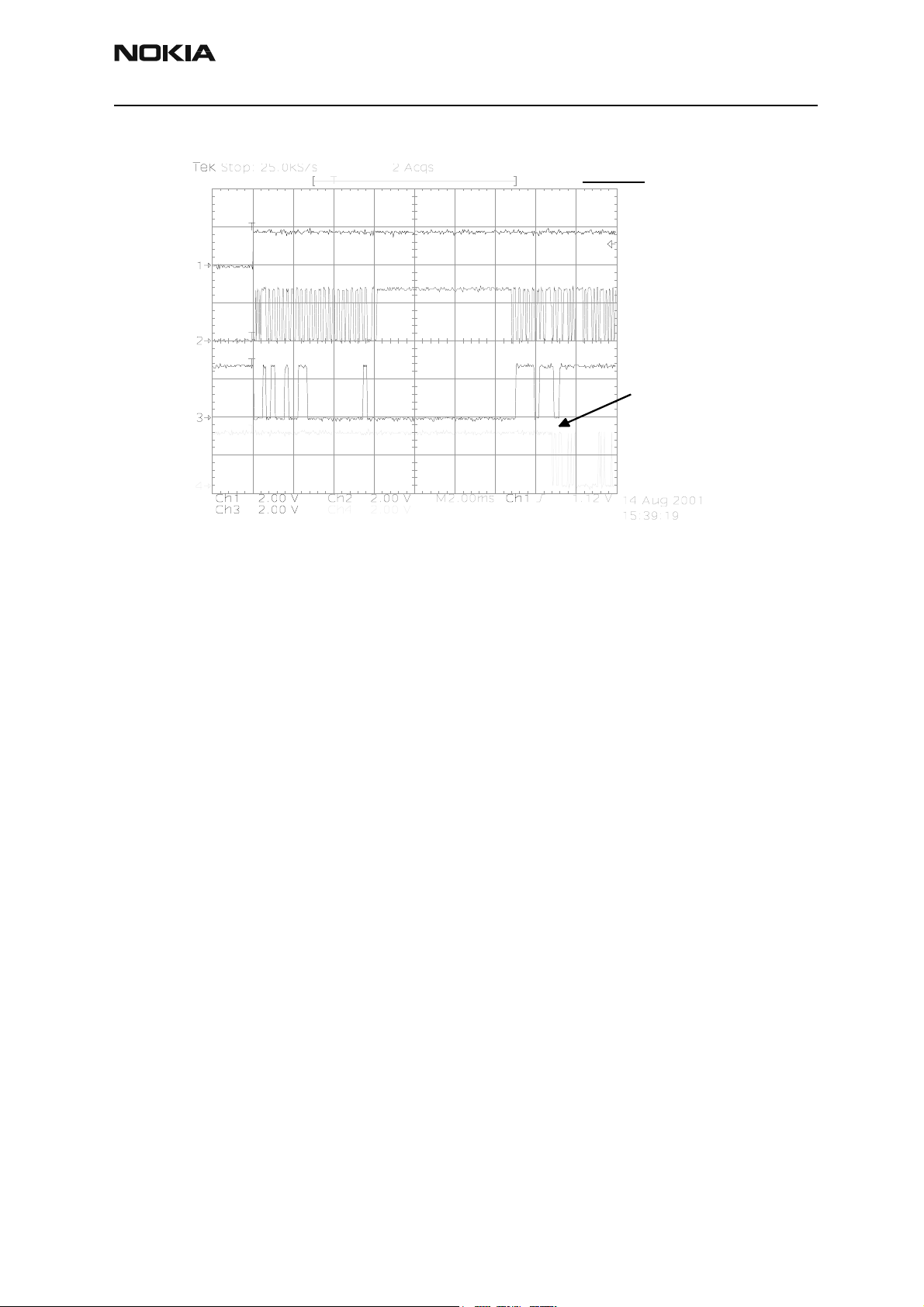
Figure 2: Flashing starts by BSI being pulled up and password being sent to UEM
• This boot code asks MCU to report prommer phone’s configuration
information, including flash device type. Now prommer can select and
send algorithm cod e to M CU SRAM (and SRAM/Fl ash self -tes ts can be
executed). (See Figure 3 on page 8 and Figure 4 on page 9.)
FLASH_2
CH1 = PURX
CH2 = MBUS
CH3 = FBUSTX
CH4 = FBUSRX
Measure points
Production test patter
(J396)
Figure 3: Flashing, continued
Page 8 Nokia Corporation Confidential Issue 1 06/2003
Page 9
RH-3
CCS Technical Documentation Troubleshooting — BB
FLASH_3
CH1 = PURX
CH2 = MBUS
CH3 = FBUSTX
CH4 = FBUSRX
Measure points
Production test pattern
(J396)
Data transfer has
started (Fbus_Rx)
Power Up and Reset
Power up and reset is controlled by the UEM ASIC. RH-3 baseband can be powered up in
the following ways:
• By the Power button, which means grounding the PWRONX pin of the
UEM
• By connect t he charger to the char ger input
• By the RTC Alarm, when the RTC logic has been programmed to give
an alarm
After receiving one of the above signals, the UEM counts a 20ms delay and then enters
its reset mode. The watchdog starts up, and if the battery voltage is greater than Vcoff+,
a 200ms delay is started to allow references, etc. to settle. After this delay elapses, the
VFLASH1 regulator is enabled. Then, 500us later VR3, VANA, VIO, and VCORE are enabled.
Finally the Power Up Reset (PURX ) line is held low for 20 ms. This reset, PURX, is sent to
UPP; resets are generated for the MCU and the DSP. During this reset phase, the UEM
forces the VCTCXO regulator on — regardless of the status of the sleep control input signal to the UEM. The FLSRSTx from the UPP is used to reset the flash during power up and
to put the flash in power down during sleep. All baseband regulators are switched on at
the UEM power on — except for the SIM regulator and Vflash2. Vsim and Vflash2 are not
used. The UEM internal watchdogs are running during the UEM reset state, with the
longest watchdog time selected. If the watchdog expires, the UEM returns to power off
state. The UEM watchdogs are internally acknowledged at the rising edge of the PURX
signal in order to always give the same watchdog response time to the MCU.
Figure 4: Flashing, continued
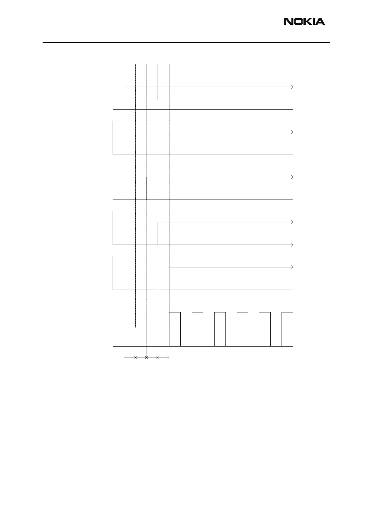
The following timing diagram (Figure 5 on page 10) represents UEM start-up sequence
Issue 1 06/2003 Nokia Corporation Confidential Page 9
Page 10
RH-3
Troubleshooting — BB CCS Technical Documentation
from reset to power-on mode.
Reference signal
PwrOnX
Charger Detection
RTC
UEMRSTX
VFlash1
VIO
VCORE
VANA
VR3
19.2MHz Clk
PURX
32kHz XTAL
t1 t2 t4t3
t1 = 20ms
t2 = 200ms
t3 = 500us
t4 = 20ms
Figure 5: Power on sequence and timing
Page 10 Nokia Corporation Confidential Issue 1 06/2003
Page 11

RH-3
CCS Technical Documentation Troubleshooting — BB
Figure 6: Measured power on sequence and timing
Power up with PWR key
When the Power on key is pressed, the UEM enters the power-up sequence. Pressing the
power key causes the PWRONX pin on the UEM to be grounded. The UEM PWRONX signal is not part of the keypad matrix. The power key is only connected to the UEM. This
means that when pressing the power key an interrupt is generated to the UPP that starts
the MCU. The MCU then reads the UEM interrupt register and notice that it is a PWRONX
interrupt. The MCU now reads the status of the PWRONX signal using the UEM control
bus, CBUS. If the PWRONX signal stays low for a certain time the MCU accepts this as a
valid power on state and continues with the SW initialization of the baseband. If the
power on key does not indicate a valid power-on situation, the MCU powers off the
baseband.
Power up when charger is connected
In order to be able to detect and start charging in a cases where the main battery is fully
discharged (empty) and hence UEM has no supply (NO_SUPPLY or BACKUP mode of
UEM), charging is controlled by START-UP CHARGING circuitry.
Whenever VBAT level is detected to be below master reset threshold (V
controlled by START_UP charge circuitry. Connecting a charger forces VCHAR input to
rise above charger detection threshold, VCH
started. UEM generates 100mA constant output current from the connected charger’s
output voltage. As battery charges its voltage rises, and when VBAT voltage level higher
than master reset threshold limit (V
MSTR-
. By detection start-up charging is
DET+
) is detected START_UP charge is terminated.
MSTR+
), charging is
Monitoring the VBAT voltage level is done by charge control block (CHACON). MSTRX=‘1’
output reset signal (internal to UEM) is given to UEM’s RESET block when VBAT>V
MSTR+
Issue 1 06/2003 Nokia Corporation Confidential Page 11
Page 12

RH-3
Troubleshooting — BB CCS Technical Documentation
and UEM enters into reset sequence.
If VBAT is detected to fall below V
during start-up charging, charging is cancelled. It
MSTR
will restart if new rising edge on VCHAR input is detected (VCHAR rising above VCH
RTC alarm power up
If phone is in POWER_OFF mode when RTC alarm occurs the wake-up procedure. After
baseband is powered on, an interrupt is given to MCU. When RTC alarm occurs during
ACTIVE mode, the interrupt for MCU is generated.
Power off
The Baseband switch power-off mode if any of following statements is true:
• Power key is pressed
• Battery voltage is too low (VBATT < 3.2 V)
• Watchdog timer register expires
The Power-down procedure is controlled by the UEM.
Power Consumption and Operation modes
DET+
).
In the POWER-OFF mode, the power (VBAT) is supplied to UEM, VIBRA, LED-Driver, PA
and PMIC.
In the SLEEP mode, both processors, MCU and DSP, are in stand-by mode. Both processors control sleep mode. When SLEEPX signal is detected low by the UEM, the phone
enters SLEEP mode. VIO and VFLASH1 regulators are put into low quiescent current
mode, and VANA and VFLASH2 regulators are disabled. All RF regulators are disabled
during SLEEP mode. When SLEEPX signal is detected high by the UEM, the phone enters
ACTIVE mode and all functions are activated.
The sleep mode is exited either by the expiration of a sleep clock counter in the UEM or
by some external interrupt, generated by a charger connection, key press, headset connection, etc.
In sleep mode, VCTCXO is shut down and 32 kHz sleep clock oscillator is used as reference clock for the baseband.
The average current consumption of the phone in sleep mode can vary depending mainly
on SW; however, on average is about 9 mA.
In the ACTIVE mode, the phone is in normal operation, scanning for channels, listening
to a base station, transmitting and processing information. There are several sub-states
in the active mode depending on the phone present state of the phone such as: burst
reception, burst transmission, if DSP is working, etc.
Page 12 Nokia Corporation Confidential Issue 1 06/2003
Page 13

RH-3
CCS Technical Documentation Troubleshooting — BB
In active mode the RF regulators are controlled by SW writing into UEM’s registers
wanted settings: VR1A and VR1B can be enabled or disabled. VSIM can be enabled or
disabled and its output voltage can be programmed to be 1.8V or 3.3V. VR2 and VR4 VR7 can be enabled or disabled or forced into low quiescent current mode. VR3 is always
enabled in active mode and disabled during Sleep mode and cannot be control by SW.
In the CHARGING mode, the charging can be performed in parallel with any other operating mode. A BSI resistor inside the battery pack indicates the battery type/size. The
resistor value corresponds to a specific battery capacity. This capacity value is related to
the battery technology.
The battery voltage, temperature, size, and charging current are measured by the UEM,
and the charging software running in the UPP controls it.
The charging control circuitry (CHACON) inside the UEM controls the charging current
delivered from the charger to the battery and phone. The battery voltage rise is limited
by turning the UEM switch off, when the battery voltage has reached 4.2 V. Charging
current is monitored by measuring the voltage drop across a 220 mOhm resistor.
Power Distribution
In normal operation, the baseband is powered from the phone‘s battery. The battery consists of one Lithium-Ion cell capacity of 850 mAh, and some safety and protection circuits to prevent harm to the battery.
The baseband contains components that control power distribution to whole phone
excluding the power amplifier (PA), which have a continuous power rail direct from the
battery. The battery feeds power directly to following parts of the system: UEM, RF Pas,
Vibra, Buzzer, Samrtcover Interface, and LED Driver.
The heart of the power distribution to the phone is the power control block inside UEM.
It includes all the voltage regulators and feeds the power to the whole system. UEM handles hardware functions of power up so that regulators are not powered and power up
reset (PURX) are not released if battery voltage is less than 3 V.
HDCA2 Baseband is powered from five different UEM regulators (VANA, VIO, VFLASH1,
and VFLASH2) and the core voltage, which provide nominal voltages and currents
according to Table 1.
UEM supplies also voltages VR1A, VR1B, VR2, VR3, VR4, VR5, VR6, and VR7 for RF. See
Table 2.
Issue 1 06/2003 Nokia Corporation Confidential Page 13
Page 14

RH-3
Troubleshooting — BB CCS Technical Documentation
Table 1: RH-3 Baseband regulators
Regulator
VCORE 300 1.5 Output voltage selectable 1.0V/1.3V/1.5V/1.8V
VIO 150 1.8 Enabled always except during power-off mode
VFLASH1 70 2.78 Enabled always except during power-off mode
VFLASH2 40 2.78 Enabled only when the system is awake (Off
VANA 80 2.78
VSIM 25 3.0 Enabled only when SIM card is used
Regulator
VR1A 10 4.75 Enabled when cell transmitter is on
VR1B 10 4.75 Enabled when the PCS transmitter is on
Maximum current
(mA)
Maximum current
(mA)
Vout (V) Notes
Power up default 1.5V
during sleep and power off-modes)
Table 2: RH-3 RF regulators
Vout (V) Notes
VR2 100 2.78 Enabled when the transmitter is on
VR3 20 2.78 Enabled when SleepX is high
VR4 50 2.78 Enabled when the receiver is on
VR5 50 2.78 Enabled when the receiver is on
VR6 50 2.78 Enabled when the transmitter is on
VR7 45 2.78 Enabled when the receiver is on
The charge pump that is used by VR1A and VR1B is constructed around UEM. The charge
pump works with 1.2 MHz oscillator and gives a 4.75 V regulated output voltage to RF.
Clock Distribution
RFClk (19.2 MHz Analog)
The main clock signal for the baseband is generated from the voltage and temperature
controlled crystal oscillator VCTCXO (G500). This 19.2 MHz sine wave clock signal is fed
to RFCLK pin of UPP. (See Figure 7 on page 15 for the waveform.)
Page 14 Nokia Corporation Confidential Issue 1 06/2003
Page 15

RH-3
CCS Technical Documentation Troubleshooting — BB
Figure 7: Waveform of 19.2MHz clock from RF to UPP and GPS BB Asic
RFConvClk (19.2 MHz digital)
The UPP distributes the 19.2MHz internal clock to the DSP and MCU, where SW multiplies this clock by seven for the DSP and by two for the MCU. (See Figure 8 on page 15.)
Figure 8: RFCovCLk waveform
CBUSClk Interface
A 1.2 MHz clock signal is use for CBUS, which is used by the MCU to transfer data
between UEM and UPP. (See Figure 9 on page 16 for Cbus data transfer.)
Issue 1 06/2003 Nokia Corporation Confidential Page 15
Page 16

RH-3
Troubleshooting — BB CCS Technical Documentation
DBUSClk Interface
A 9.6 MHz clock signal is use for DBUS, which is used by the DSP to transfer data
between UEM and UPP. (See Figure 10 on page 16.)
Figure 9: Cbus Data Transfer
Figure 10: Dbus data transferring
The system clock is stopped during sleep mode by disabling the VCTCXO power supply
(VR3) from the UEM regulator output by turning off the controlled output signal SleepX
from UPP.
Page 16 Nokia Corporation Confidential Issue 1 06/2003
Page 17

RH-3
CCS Technical Documentation Troubleshooting — BB
SLEEPClk (Digital)
The UEM provides a 32kHz sleep clock for internal use and to UPP, where it is used for
the sleep mode timing. (Figure 11 on page 17.)
SLEEPClk (Analog)
However, when the system enters sleep mode or power off mode, the external 32KHz
crystal provides a reference to the UEM RTC circuit to turn on the phone during porwer
off or sleep mode. (See Figure 12 on page 17.)
Figure 11: 32kHz Digital output from UEM
Figure 12: 32kHz analog waveform at 32KHz crystal input
Issue 1 06/2003 Nokia Corporation Confidential Page 17
Page 18

RH-3
Troubleshooting — BB CCS Technical Documentation
Charging operation
Battery
In RH-3, a Lithium-Ion cell battery with a capacity of 850 mAh is used. Reading a resistor inside the battery pack on the BSI line indicates the battery type and size. The temperature sensor for BTEMP is inside the phone and position on the board in a way that it
always has the same temperature as ther battery itself.
Temperature and capacity information are needed for charge control. The resistor for
capacity info is connected to BSI pin of battery connector. Phone has 100 kΩ pull-up
resistors for this line so that they can be read by A/D inputs in the phone.
See Figure 13 on page 18 and Figure 14 on page 18 for the details.
Charging circuitry
The UEM ASIC controls charging depending on the charger being used and the battery
size. External components are needed for EMC, reverse polarity and transient protection
of the input to the baseband module. The charger connection is through the system connector interface. The RH-3 baseband is designed to support DCT3 chargers from an electrical point of view. Both 2- and 3-wire type chargers are supported. For the 3-wire
charger, the control line is not supported and not connected to the Baseband ASICs. See
Figure 15 on page 19 for details.
Figure 13: BL-5C battery pack pin order
Figure 14: Interconnection diagram inside the battery pack
Page 18 Nokia Corporation Confidential Issue 1 06/2003
Page 19

RH-3
)
CCS Technical Documentation Troubleshooting — BB
R200
X102 battery
Charger Detection
Connecting a charger creates voltage on VCHAR input of the UEM. When VCHAR input
voltage level is detected to rise above 2 V (VCHdet+ threshold) by UEM charging starts.
VCHARDET signal is generated to indicate the presence of the charger for the SW. The
charger identification/acceptance is controlled by EM SW.
The charger recognition is initiated when the EM SW receives a ”charger connected”
interrupt. The algorithm basically consists of the following three steps:
1 Check that the charger output (voltage and current) is within safety limits.
2 Identify the charger as a two-wire or three-wire charger.
3 Check that the charger is within the charger window (voltage and current).
If the charger is accepted and identified, the appropriate charging algorithm is initiated.
omahawk Charger
connector
X102
+ VCHAR
GND
F100
1.5A
Figure 15: Charging circuitry
L100
________
42R/100MHz
C106
1n0
V100
1PMT16AT3
0
1
2
CHARGER(4:0
GND
Figure 16: Charging circuit
Issue 1 06/2003 Nokia Corporation Confidential Page 19
Page 20

RH-3
Troubleshooting — BB CCS Technical Documentation
Charge Control
In active mode charging is controlled by UEM’s digital part. Charging voltage and current
monitoring is used to limit charging into safe area. For that reason UEM has programmable charging cut-off limits:
VBATLim1=3.6 V (Default)
VBATLim2L=5.0 V and
VBATLim2H=5.25 V.
VBATLim1, 2L, 2H are designed with hystereses. When the voltage rises above VBATLim1,
2L, 2H+ charging is stopped by turning charging switch OFF. No change in operational
mode is done. After voltage has decreased below VBATLim- charging re-starts.
There are two PWM frequencies in use depending on the type of the charger: two-wire
charger uses a 1Hz and a three-wire charger uses a 32Hz. Duty cycle range is 0% to
100%. Maximum charging current is limited to 1.2 A.
Audio
The audio control and processing in RH-3 is provided by UEM, which contains the audio
codec, and UPP — which contains the MCU and DSP blocks, handling and processing the
audio data signals.
The baseband supports three microphone inputs and two earpiece outputs. The microphone inputs are MIC1, MIC2, and MIC3. MIC1 input is used for the phone's internal
microphone; MIC2 input is used for headsets (HDB-4, BHF-1. and CarK-126), Loopset
(LPS-4). MIC3 input is used for third-party accessories (2.5mm Jack). Every microphone
input can have either a differential or single ended ac connection to UEM circuit. In
RH-3, the internal microphone (MIC1) and MIC2 are differential and MIC3 microphones
are single-ended. The microphone signals from different sources are connected to separate inputs at UEM. Inputs for the microphone signals are differential type. Also,
MICBIAS1 is used for MIC1 and MICBIAS2 is used for MIC2 and MIC3.
Display and Keyboard
LEDs are used for LCD and keypad illumination in RH-3. There are three LEDs for LCD and
four LEDs for keypad. The LEDs are supplied by a driver circuit which consists of a charge
pump and several current source, which are partly integrated into the driver and partly
realized by discretes.
A monochrome LCD is used in RH-3. Interface is using 9-bit data transfer. The interface
is quite similar to DCT3 type interface, except Command/Data information is transferred
together with the data. D/C bit set during each transmitted byte by MCU SW.
Figure 17 on page 21 is the waveform for LCD interface.
Page 20 Nokia Corporation Confidential Issue 1 06/2003
Page 21

RH-3
CCS Technical Documentation Troubleshooting — BB
Accessory
RH-3 is designed to support differential ended external audio accessory connection.
Headset and data cables can be directly connected to system connector or 2.5mm jack
supporting TTY/TDD or universal headset. Detection of the different accessories is based
on the ACI code residing inside the accessories except for basic headset (HDB-4) and
universal headset. The UHJ is detected by the interrupt generated on GenIO (12). The
basic headset is detected via ACI detection algorithm. However, the ACI pin is always
grounded.
It is end user's responsibility to set the phone for TTY/TDD since there are too many different TTY/TDD devices to be detected.
Figure 17: LCD Interface
Issue 1 06/2003 Nokia Corporation Confidential Page 21
Page 22

RH-3
Troubleshooting — BB CCS Technical Documentation
Test Points
FBUSRX
PURX
DBUSCLK
VR5
VR3
MBUSRX
VR7
VR4
CBUSCLK
GENIO17
GENIO16
GENIO18
MBUSTX
FBUSTX
GENIO14
RFCONVCLK
GENIO15
UEMRSTX
BSI
VIO
VR2
VR6
Vcore
VR1B
VR1A VFlash1
VANA
Figure 18: RH-3 BB test points, regulators, and BB ASICs
Page 22 Nokia Corporation Confidential Issue 1 06/2003
Page 23

RH-3
CCS Technical Documentation Troubleshooting — BB
RFCLK
GPSCLK
FBUSTX FBUSRX
Troubleshooting
The following hints should help finding the cause of the problem when the circuitry
seems to be faulty. Troubleshooting instructions are divided following sections:
1 Top troubleshooting map
2 Phone is totally dead
3 Power doesn‘t stay on or the phone is jammed
4 Flash programming doesn‘t work
5 Display is not working
6 Audio fault
RTCCLK
Figure 19: RH-3 BB test points, regulators, and BB ASICs
Vpp
MBUS
GND
7 Charging fault
First, carry out a through visual check of the module. Ensure in particular that:
• there are no mec hanical damages
• soldered joints are OK
• ASIC orientations are OK
Issue 1 06/2003 Nokia Corporation Confidential Page 23
Page 24

RH-3
Troubleshooting — BB CCS Technical Documentation
Top troubleshooting map
Top
y
l
l
a
t
o
t
e
d
n
a
o
e
h
d
P
NO
n
i
m
m
r
a
r
o
g
w
o
r
t
'
p
n
s
h
e
s
o
a
l
d
F
YES
g
k
YES
Phone dead
Flash faults
NO
t
'
n
e
s
n
e
o
o
h
d
p
d
r
e
e
o
n
o
m
p
h
u
m
P
t
a
r
j
a
t
s
i
s
NO
t
'
n
s
e
o
d
g
k
n
r
i
o
g
r
w
a
h
C
YES
Phone is jammed
YES
NO
Charger
Top 2
Page 24 Nokia Corporation Confidential Issue 1 06/2003
Page 25

RH-3
CCS Technical Documentation Troubleshooting — BB
Top 2
s
t
l
u
a
f
o
i
d
u
A
NO
s
D
E
L
g
r
n
i
o
k
y
r
a
o
l
w
p
s
t
i
o
D
n
YES
YES
Audio faults
Display faults
NO
t
'
n
s
e
o
d
k
d
r
a
o
p
w
y
e
K
YES
Keypad faults
END
Issue 1 06/2003 Nokia Corporation Confidential Page 25
Page 26

RH-3
Troubleshooting — BB CCS Technical Documentation
Phone is totally dead
Phone is
dead
- If current is zero check X110
solder and VBATT lines
-If current is too high check for
shorts
- Make sure all BB regulators are at
their respective voltage levels like
VANA, VIO, VCORE), VFlash1, and
VR3. See phone's top view diagram
for test po in ts .
- Make sure the System C lk is
19.2MHz and that the Sleep Clk is
32KHz
- Also make sure PURX and SleepX
signals are high (1.8V).
Phone current is
zero or too high?
No
Yes
Phone current is
<= 30 mA
No
Phone current is
35 mA
Yes
Is phone in LOCAL
MODE ?
Yes
No
No
Is phone flash
programming O K?
Ch eck BS I line
X110, R202,
R203, C230. Are
they OK?
No
Yes
Yes
Phone is
jam med
Flash
faults
Change UEM
Yes
OK restart
No
Repair
Page 26 Nokia Corporation Confidential Issue 1 06/2003
Page 27

RH-3
CCS Technical Documentation Troubleshooting — BB
Flash programming doesn‘t work
Flash
faults
The phone does
not set Flashbus
TXD line high after
the startup.
No
The phone does
not set Flashbus
TXD line low after
the line has been
high.
Yes
Change
UEM
Measure BSI pulse
during Flash
programming.
Is it OK?
Yes
Measure FBusRx
(2.78V) signal during
flash programming at
the bottom connector
and Flash pads. Does
waveform match Figure
1?
s
e
Y
No
Check BSI line
X110, C230,
R203, R202
Check R100,
R101, R104,
N
o
C104, C105 and
V101. If OK, then
change UEM or
UPP
o
N
Flash
faults
page 2
Issue 1 06/2003 Nokia Corporation Confidential Page 27
Page 28

RH-3
Troubleshooting — BB CCS Technical Documentation
Flash
Faults
page 2
Can you read the
m a n u fa c tu re r ID
and the Device
ID ?
Yes
Is the pho ne tota lly
dead?
No
No
Yes
Change Flash
Phone is
dead
Phone doesn't
start up or the
phone is jamm ed?
No
Retest
Yes
Phone is
jammed
Page 28 Nokia Corporation Confidential Issue 1 06/2003
Page 29

RH-3
CCS Technical Documentation Troubleshooting — BB
Power doesn‘t stay on or the phone is jammed
Phone is
jammed
Check VBATT,
VIO, VCORE, VFlash1,
Measure VIO,
VCORE, Vflash1,
VANA, and VR3
votages. Are they
OK ?
Yes
No
VANA, VR3 capacitors.
Are they OK ?
See phones top view
diagram for cap
location.
No
Yes
Check BSI/BTEMP
lines and VBATT lines
if OK change UEM
Repair
Measure 32kHz
Sleep Clk from
testpoint .
Is it OK?
Yes
Measure
19.2MHz RF Clk at
testpoint C502.
Is it OK?
Yes
Measure PURX
and SleepX at test
points TP1 and
TP2. Are they high
(1.8V) ?
Yes
No
No
No
Measure the
32kHz Clk crystal .
Is it OK?
Yes
Measure
the 19.2MHz Clk
coming from the
VCTCXO at C524.
Is it OK ?
Yes
No
No
Change B200
Change UEM
Check 19.2MHz
generator in RF section
(G503, C505, C520,
C502, C523, C525,
C524, R511, R510,
R512, R520, R521,
R522, R517, R518,
VR1A and VR3.) If OK,
change G501.
Change UPP
Jammed
page 2
Change UEM
Issue 1 06/2003 Nokia Corporation Confidential Page 29
Page 30

RH-3
Troubleshooting — BB CCS Technical Documentation
Jammed
Page 2
Phone shutdown
after 32 seconds
No
Read phone info.
Is it OK?
s
e
Y
Yes
Has the phone
being flashed?
Yes
No
Flash the phone
Change UPP and
reflash. If problem
still exists, change
UEM and reflash the
phone.
Retest
Page 30 Nokia Corporation Confidential Issue 1 06/2003
Page 31

RH-3
CCS Technical Documentation Troubleshooting — BB
Charger
Charger
Connect Charger
Make sure battery is
connedted.
Battery bar doesn't
work (scroll)
Yes
Measure voltage
over V100.
Is it > 3.0 Vdc?
Yes
Read BTEMP value.
Is it ~ 25C (0319)?
No
No
No
Retest
Check X101, X102,
F100, L100, V100,
C106.
Change UEM
Yes
Remove (fuse)
F100 and measure
current.
Is it ~350-390 mA?
Yes
No
Change UEM
Retest
Issue 1 06/2003 Nokia Corporation Confidential Page 31
Page 32

RH-3
,
Troubleshooting — BB CCS Technical Documentation
Audio faults
Audio
faults
Is the earpiece
working?
Yes
No
Change earpiece.
Is it working now?
Set phone in LOCAL mode.
Use Phoenix "Baseband Audio
Control" and set the following:
Enable Tx, Enable Rx, Select
MIC2 (0dB), Enable earpiece
and enable digital loop back
Inject a 1KHz sine signal
20mVp-p on XMIC (pin9/10 of
the bottom connector
Is the signal coming
out of the UEM on
EARP and EARN?
only.
No
Yes
No
Retest
Probe signal on
R162, R155, V152,
C154, C155, R152,
R150, C151, C153,
L120, R180. Check
the bias voltage on
one end of C193
(2.1V). If OK,
change UEM
Yes
Check R150, C180
and C181.
If OK, then change
earpiece.
Yes
Audio
faults 2
Page 32 Nokia Corporation Confidential Issue 1 06/2003
Page 33

RH-3
CCS Technical Documentation Troubleshooting — BB
Audio
faults 2
Is the microphone
working?
Yes
No
Use Phoenix "Baseband Audio
Control" and set the following: E nabl e
Tx, Enable Rx, Select MIC1, Enable
Talk through the microphone.
Change the
microphone.
Is it working now?
No
Set phone in LOCAL mode.
HF only (differential ended).
Measure MICB1 at
C195. Is it ~2.1V?
Yes
Yes
No
Retest
Check C195, R176,
R178. If OK, change
UEM
Audio
faults 3
Is the signal going
to the UEM at MICP
and MICN at L122
and C174?
Yes
Is the signal going
out of the UEM at
XEAR, pin 10 on the
bottom connector?
Yes
No
No
If connection is OK
at C175 and L122,
then change
microphone
Check if R160 is
shorted to GND. If
OK, change UEM
Retest
Issue 1 06/2003 Nokia Corporation Confidential Page 33
Page 34

RH-3
Troubleshooting — BB CCS Technical Documentation
Audio
faults 3
Is MIDI working?
Yes
No
Measure VBATT
voltage from C196.
Is it OK?
Yes
Set phone in LOCAL mode.
Use Phoenix to digital loop MIC1
to HF single-ended output. Also,
set GenIO(28) high.
Talk to MIC1. Check
signal @C157. Is
signal OK?
Yes
No
No
Check VBATT line.
Change the UEM
Check signal
Audio
faults 4
@MIDI speaker
pads. Is signal OK?
N
e
Y
s
Change speaker
o
Change MIDI
amplifier N150
Page 34 Nokia Corporation Confidential Issue 1 06/2003
Page 35

RH-3
CCS Technical Documentation Troubleshooting — BB
Audio
faults 4
Is VIBRA working?
Yes
No
Measure VBATT
voltage pin 1 of
M300.
Is it OK?
Yes
Set phone in LOCAL mode.
Use Phoenix "Message Sender"
and navigate as follows:
DEV_HOST --> DEV_PC -->
PN_ACCESSORY -->
PN_OBJ_ROUTING_REQ -->
PN_OBJ_PC --> UTID_100 -->
ACC_VIBRA_CTRL_REQ.
Select "ACC_ON" and click
"Send'
Measure the UEM
signal on pin 2 of
M300.
Is the signal OK?
No
Check VBATT line.
No
Change the UEM
Yes
Change VIBRA
END
Issue 1 06/2003 Nokia Corporation Confidential Page 35
Page 36

RH-3
Troubleshooting — BB CCS Technical Documentation
Display faults
Display
faults
Are the UI module
LEDs turned on
when phone is
turned on or when
making a phone
call?
N
o
Measure VBATT
voltage at C310.
Is it OK?
Yes
No
Check VBATT line.
Set phone in LOCAL mode.
Use Phoenix "Message Sender" and
navigate down as follows: DEV_HOST --
> DEV_PC --> PN_LIGHT -->
OBJ_ROUTING_REQ --> OBJ_PC -->
UTID --> LIGHT_CONTROL_REQ -->
LIGHT_CONTROL_TARGER_KBD.
Select "LIGHT_STATE_BLINK" and
Yes
Measure the UEM
signal @R306. Is
the signal OK?
Measure the voltage
@LEDs. Is it ~3.8V?
Yes
click "Send'
Yes
Yes
No Change the UEM
No
Change LM2795
Yes
Display
faults 2
Change LEDs
Page 36 Nokia Corporation Confidential Issue 1 06/2003
Page 37

RH-3
CCS Technical Documentation Troubleshooting — BB
Display
faults 2
Does the Display
start?
Yes
Try changing
No
Use Phoenix "Message Sender" and
PN_TEST --> OBJ_ROUTING_REQ
TEST_DISPLAY_SET -->NUM_SB --
> TEST_SB_UI_DISPLAY_PATTERN
"TEST_PATTERN_ALTPIXELS"and
display module.
Does it work?
o
N
Set phone in LOCAL mode.
navigate down as follows:
DEV_HOST --> DEV_PC -->
--> OBJ_PC --> UTID -->
TEST_UI_TEST_REQ -->
-->SB_LENGTH. Select
click "Send"
Check signal @ pin
1 ("1"), 2 ("0"), 4
(data), and 5
(clock). Are the
signals OK?
No
s
e
Y
Retest
Change UPP
Yes
END
Change Display
Issue 1 06/2003 Nokia Corporation Confidential Page 37
Page 38

RH-3
Troubleshooting — BB CCS Technical Documentation
Keypad faults
Keypad
faults
Is the power key
working?
s
e
Y
Keypad
faults 2
No
Measure voltage at
S300. Is it High?
Yes
Measure voltage at
S300 when power
key is pressed. Is it
High?
o
N
No
Y
e
s
Check S300 and
R304. If OK, change
UEM
Change S300
Phone is
jammed
Page 38 Nokia Corporation Confidential Issue 1 06/2003
Page 39

RH-3
CCS Technical Documentation Troubleshooting — BB
Keypad
faults 2
Press
malfunctioning key
or keys. Are the
signals correct?
o
N
Yes
Retest
Change Z300. Are
the signals correct?
o
N
Yes
Retest all key
presses
Change UPP
(D400)
Issue 1 06/2003 Nokia Corporation Confidential Page 39
Page 40

RH-3
Troubleshooting — BB CCS Technical Documentation
Page 40 Nokia Corporation Confidential Issue 1 06/2003
 Loading...