

Page 1

CCS Technical Documentation
RH-3 Series Transceivers
Troubleshooting — GPS
Issue 1 06/2003 Confidential Nokia Corporation
Page 2
RH-3
Troubleshooting — GPS CCS Technical Documentation
Page 2 Nokia Corporation Confidential Issue 1 06/2003
Page 3

RH-3
CCS Technical Documentation Troubleshooting — GPS
Contents
Page No
Troubleshooting - Global Positioning System (GPS) Engine........................................ 5
Acronyms and Abbreviations......................................................................................... 6
Troubleshooting the GPS BB ......................................................................................7
Troubleshooting Flowchart....................................................................................... 7
Flowchart Notes ...................................................................................................... 10
Troubleshooting the GPS RF .....................................................................................13
Limitations .............................................................................................................. 13
GPS Receiver .............................................................................................................13
General Instructions ................................................................................................ 13
Test Equipment ..........................................................................................................14
Path of the Received Signal .......................................................................................14
GPS RF Quick Fault-finding Chart ...........................................................................15
GPS RF Circuitry and Component Placement ...........................................................16
GPS Module Test Points ............................................................................................17
GPS RF General Checking ........................................................................................18
GPS Reference Clock Checking ................................................................................21
GPS RF and GPS BB Interface Checking .................................................................23
GPS RX Chain Checking ...........................................................................................24
Issue 1 06/2003 Nokia Corporation Confidential Page 3
Page 4

RH-3
Troubleshooting — GPS CCS Technical Documentation
Page 4 Nokia Corporation Confidential Issue 1 06/2003
Page 5
RH-3
CCS Technical Documentation Troubleshooting — GPS
Troubleshooting - Global Positioning System (GPS) Engine
The RH-3 Model 2285 handset supports 800 CDMA / 1900 CDMA + GPS with IS 2000
capability. The RH-3P Model 2270 supports PCS and GPS functionality for Enhanced 911
(E911) services.
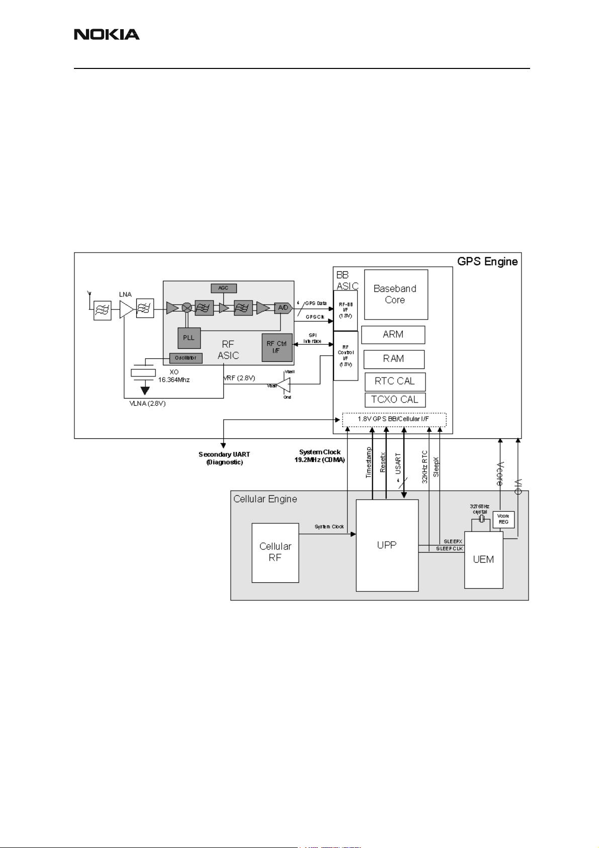
GPS circuitry utilizes RF signals from satellites stationed in geosynchronous orbit to
determine latitude and longitude of the handset. The GPS circuitry and the cellular
engine (CE) circuitry are completely separate in the handset. The GPS circuitry is located
exclusively on the secondary side of the PWB.
See Figure 1 for the General Block Diagram.
Figure 1: GPS Block Diagram
Issue 1 06/2003 Nokia Corporation Confidential Page 5
Page 6
RH-3
Troubleshooting — GPS CCS Technical Documentation
Acronyms and Abbreviations
AGPS Assisted GPS
AMPS Advanced Mobile Phone Service
ASIC Application Specific Integrated Circuit
E911 Enhanced 911
FCC Federal Communications Commission
BPSK Binary Phase Shift Keying
BT BlueTooth
C/A Coarse Acquisition-Code
CE Concurrent Engineering
CDMA Code Division Multiple Access
C/No Carrier to Noise ratio [dB-Hz]
DCT Digital Core Technology
DSSS Direct Sequence Spread Spectrum
FCC Federal Communications Commission
GPS Navstar Global Positioning System
HW Hardware
IC Integrated Circuit
L1 Link 1
LPRF Low Power RF
NF Noise Figure
PCS Personal Communications Service
PRN Pseudo Random Noise
PSAP Public Safety Answering Point
PWB Printed Wiring Board
Page 6 Nokia Corporation Confidential Issue 1 06/2003
Page 7

RH-3
CCS Technical Documentation Troubleshooting — GPS
RF Radio Frequency
RHCP Right Hand Circular Polarized
SA Selective Availability
SPS Standard Positioning Service
UTC Universal Time Coordinated
WB Wideband
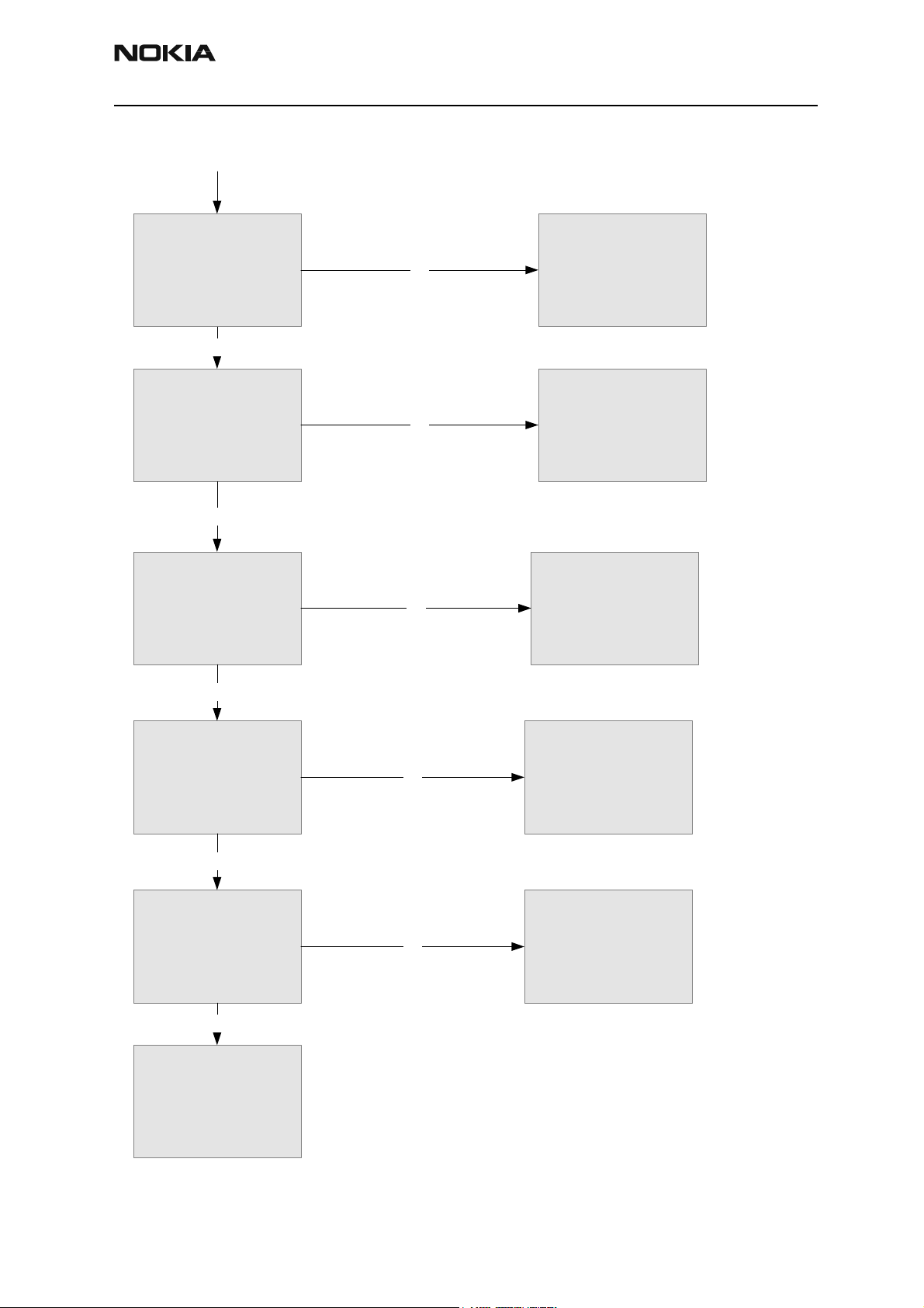
Troubleshooting the GPS BB
Figure 2: GPS RF-BB ASIC Interface
To troubleshoot the GPS BB, put the GPS engine (GE) and cellular engine (CE) in the
proper mode by selecting the GPS Testing drop-down menu item from the “Troubleshooting” dialog box. Ensure that the necessary inputs from the CE are good (e.g., power, clock,
and so on). Next, ensure that these inputs produce the proper outputs. Due to the large
level of integration (most functionality is contained in the two ASIC chips), the diagnostics that may be performed are limited.
Visually inspect the GPS circuitry to determine if the problem is physical (dislodged parts,
corrosion, poor solder joints, and so on) prior to performing any diagnostics.
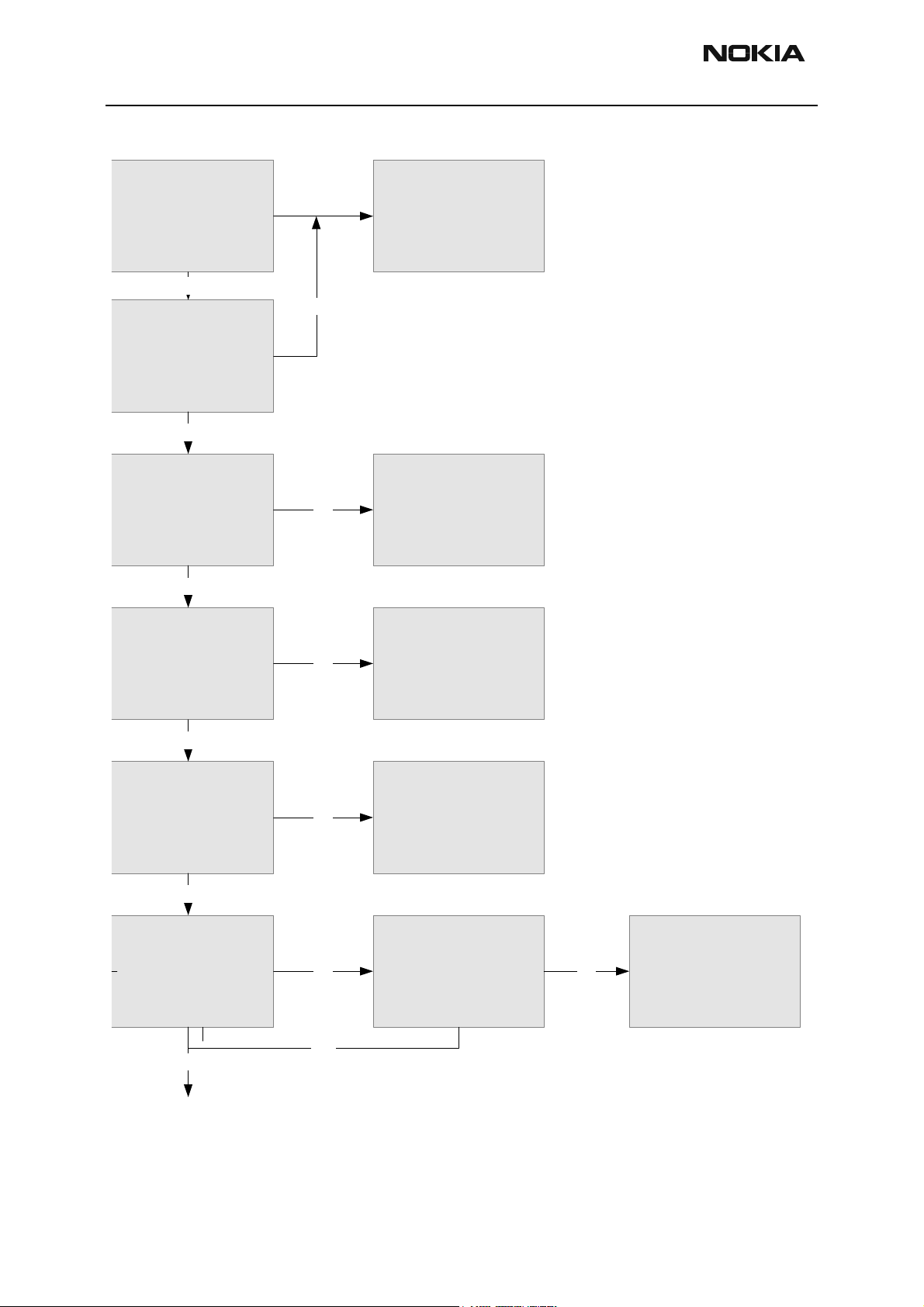
Troubleshooting Flowchart
Before implementing the flowchart, turn the GPS section ON in the “GPS Receiver Control (AMS)” tab of the GPS component in Phoenix.
Reference Table 1 for GPS Test Points assignment and Figure 10 for GPS Test
Points locations.
Issue 1 06/2003 Nokia Corporation Confidential Page 7
Page 8
RH-3
Troubleshooting — GPS CCS Technical Documentation
Vcore at 1.5V?
Yes
VIO at 1.8V ?
(@ C018)
Yes
GPS_RF_CLK
(19.2MHz) OK?
(J062)
Yes
GPS_EN_RESET is
held high?
(J061)
No
No
No
Troubleshoot CE
power supply
Troubleshoot CE
VCTCXO circuit
BB ASIC being held in
reset, troubleshoot
source in CE
Yes
GPS_SLEEPCLK
(32.768KHz) OK?
(J063)
Yes
VRF_GPS OK?
Yes
No
No No
Yes
Troubleshoot CE
sleep clock circuit
VRF_GPS regulator
enable line low?
Replace regulator
N052
Page 8 Nokia Corporation Confidential Issue 1 06/2003
Page 9
RH-3
CCS Technical Documentation Troubleshooting — GPS
GPS_CLK
(16.368MHz) OK?
(J010)
Yes
Test Mode 1 OK?
Yes
CE sending code
download signals?
Yes
No
No
No
Replace TCXO or
GPS RF ASIC
Replace GPS BB
ASIC
Determine why CE not
sending download
signals
SPI interface active?
Yes
RF data and clock?
Yes
Debug RF front end
No
No
Replace GPS BB
ASIC
Replace GPS RF
ASIC
Issue 1 06/2003 Nokia Corporation Confidential Page 9
Page 10

RH-3
Troubleshooting — GPS CCS Technical Documentation
Flowchart Notes
Clocks and Power
The proper GPS_RF_CLK is a 19.2 MHz, approximately 800mV peak-to-peak sine wave
(see Figure 3).
Figure 3: 19.2MHz System Clock
The GPS_CLK should be a 16.3MHz, 1.8V peak-to-peak square wave (see Figure 4).
Figure 4: GPS_CLK
Page 10 Nokia Corporation Confidential Issue 1 06/2003
Page 11

RH-3
CCS Technical Documentation Troubleshooting — GPS
Test Mode 1
Test Mode 1 is a built-in self-test (BIST) for the GPS BB ASIC that checks for internal
faults. To implement Test Mode 1, select the test mode 1 radio button and then click the
Execute button in the “Rx simple actions” tab of the GPS component in Phoenix.
Code Download
The code store inside the GPS BB ASIC is volatile. As a result, each time power is applied
to the ASIC, the code that runs there must be re-downloaded from the CE. If this process
does not complete correctly, the GE will not work. The interface protocol utilized for this
process is the Universal Synch/Asynch Receiver Transmitter (USART), and the pins on the
GPS BB ASIC are labeled U1Tx, U1Rx, U1_DATA_RDY, and U1_CLK. To determine if this
interface is active, check for activity on these lines at power up. Each of these lines
should have a short burst of activity immediately after power is applied. To capture these
signals, you will need to set the storage scope to single sweep or triggered mode (see
Figure 5).
Figure 5: GPS Code Download U1 CLK U1 RX
SPI Interface
The SPI interface is a three-line synchronous serial interface used by the GPS BB to communicate to the GPS RF. These lines are called SPI_CLK, SPI_DATA, and SPI_EN. Activity
should be seen for a short period on these signals each time a mode switch is made (e.g.,
between idle and off mode in the “Rx simple actions” tab of the GPS component in Phoenix). See Figure 6.
Issue 1 06/2003 Nokia Corporation Confidential Page 11
Page 12

RH-3
Troubleshooting — GPS CCS Technical Documentation
RF Data and Clock
The GPS RF ASIC sends encoded raw GPS data to the GPS BB ASIC for further processing
via a four-line synchronous parallel interface. These signals are data (labeled B0, B1, B2,
and B3) and GPS_CLK. The GPS_CLK has been previously tested (see the flowchart). The
four-data lines should show continuous activity almost immediately after power has
been applied to the phone (see Figure 7).
Figure 6: Spi Data and Clock
Figure 7: RF Data and Clock
Page 12 Nokia Corporation Confidential Issue 1 06/2003
Page 13

RH-3
CCS Technical Documentation Troubleshooting — GPS
Troubleshooting the GPS RF
The purpose of this section is to define GPS test limits on the product line and to guide
the GPS RF troubleshooting.
Limitations
Measurements should be done using High-Frequency Probe with spectrum analyzer in
order to measure local and reference frequencies and RF-power levels in intermediate
stages of chain. Oscilloscope is used to measure DC-voltages and low frequency signals.
Digital multimeter is also useful measurement equipment in faultfinding. Also cellular
tester is needed in order to perform tests mentioned in this section.
External RF connector is implemented for improving reliability of the measurements and
should be used when reasonable.
GPS RF-section is mainly build around of TRF5101 PG2.1 IC (N054) ASIC. The GPS RF
block has a separate front end filter, inter stage filter, LNA, TCXO, and down converter
circuitry.
In this RF troubleshooting section, tolerances are specified for critical GPS RF signals and
voltages.
Before changing a single ASIC or component, please check the following items:
1 The soldering and alignment marks of the GPS ASICs
2 Supply voltages and control signals are OK
NOTE 1: The RF ASIC module is static discharge sensitive! It is recommended that EDS-protected
clothes and shoes are worn and that grounded soldering irons are used.
NOTE 2:The shield lid must be always replaced with new one after it is opened. Check that there are
no short circuits on PWB caused by plate ends.
GPS Receiver
General Instructions
Receiver troubleshooting is divided into four sections:
1 GPS RF general checking
2 GPS reference clock checking
3 GPS RF and GPS BB interface checking
4 GPS RX chain checking
The fastest way to troubleshoot GPS RF is to follow the GPS RF Fault-finding chart Quick
Issue 1 06/2003 Nokia Corporation Confidential Page 13
Page 14

RH-3
C
K
ADCout
IFout
GPS Clock
LO/8 Te
st
1
Troubleshooting — GPS CCS Technical Documentation
Reference (See Figure 9).
Please note that before changing ASICs or filters, soldering and missing components
must be checked visually. There are no parameters in GPS RF, which should be tuned
externally. Accurate signal levels are not shown in the flowcharts below because of the
figures apply with specific measurement probes. It is useful to compare the results
against reference phones.
Test Equipment
1 Signal generator up to 2 GHz
2 Oscilloscope with 10:1 passive probe
3 High Frequency Probe for Spectrum Analyzer (Please note that the signal levels
mentioned in the RX troubleshooting have been measured with an active probe.)
4 Spectrum analyzer up to 6.7 GHz
5 PC with Phoenix SW and GPS option
Path of the Received Signal
575.42 MHz
4.092MH z
LNA
BPF
SAW
16. 36 8 MH z
TCXO
Im age Reject
Mixer
÷ 2
Loop
Filte r
fco mp=16.368 MHz
Oscillator
VCO
Tank
LO =157 1 .328 MHz
÷ 2
÷ 8
÷1 2
Ph ase
Det
AG C
4 Bit
ADC
LO/8 Test Point
196.416 MHz
Programming
In terf ace
IF out Test
Points
DATA
LOC
ENABLE
SPI
Figure 8: GPS RF Functional Diagram
Page 14 Nokia Corporation Confidential Issue 1 06/2003
Page 15

RH-3
CCS Technical Documentation Troubleshooting — GPS
GPS RF Quick Fault-finding Chart
Apply 1575.520152 MHz @ -110 dBm
CW sign al to external GPS RF
connector/ s witch and run
Troubleshooting/GPS Testing/GPS
Quick Test/Galvanic
Not OK
Apply 1575.520152 MHz @ -100 dBm
CW sign al to external GPS RF
connector/ s witch and run
Troubleshooting/GPS Testing/GPS
Receiver Control (AMS)/Receiver ON
Not OK
Check 19.2 MHz
GPS_RFCLK si gnal J009
OK
Check 16.368 MHz
GPS_CLK signal J008
OK
Check the 196 .416 MHz LO/8
at J005
OK
Not OK
Not OK
Not OK
Start CDMA t roubleshooting,
VCTCXO, etc.
Measure VRF_GPS at C017 Replace regulator N051
OK
Replace TCXO B001
Measure VIO at C067
OK
Replace GPS RF ASIC N054
Not OK
Not OK
Start CDMA BB
troubleshooting, UEM, etc.
Check signal level Z003
output (L005)
OK
Check signal level at V001
output (C010)
OK
Check signal level at N054
input (C069)
Not OK
Not OK
Not OK
Replace filter Z003
Replace transistor V001
Replace filter Z004
Figure 9: GPS RF Fault-finding chart (Quick Reference)
Issue 1 06/2003 Nokia Corporation Confidential Page 15
Page 16

RH-3
Troubleshooting — GPS CCS Technical Documentation
GPS RF Circuitry and Component Placement
Note: GPS RF Schematics are located in Schematics section of this Service Manual.
Table 1: GPS Engine Test Points Table
J004 Test_IF_P
J003 Test_IF_M
J005 LO/8
J002 GPS_SPI_CLK
J007 GPS_SPI_DATA
J008 GPS_SPI_EN
J006 XTAL 2
J008 GPS_CLK
GND
J001 GPS_U2TX
R044 GPS_U2RX
J017 GPS_PA_EN
J011 GPS_SLEEPX
J015 GPS_U1_DATA_RDY-TIMESTAMP
J013 GPS_U1_RX
J014 GPS_U1_TX
J016 GPS_INT_U1_CLK
J012 GPS_EN_RESET
J009 GPS_RFCLK (19.2 MHZ)
Page 16 Nokia Corporation Confidential Issue 1 06/2003
Page 17

RH-3
CCS Technical Documentation Troubleshooting — GPS
GPS Module Test Points
J007
J002
J005
C069
J003
J004
C067
J008
C017
J006
J009
J012
R044
J001 J017 J011 J010
L005
J016
J014
J015
J013
C010
Figure 10: GPS Component Placement (PWB Bottom Side)
Issue 1 06/2003 Nokia Corporation Confidential Page 17
Page 18

RH-3
Troubleshooting — GPS CCS Technical Documentation
GPS RF General Checking
The fastest way to get an overview of GPS RF status is to run GPS QUICK TEST. This can
be done by using a CW signal generator and Phoenix. When running Galvanic testing, set
signal generator frequency to 1575.520152 MHz and adjust level to -110 dBm at GPS
antenna port. In radiated testing CW level has to be higher, because of the attenuation in
pad + cable + coupler. With -20 dB pad signal level in signal generator is ~ -110 dBm +
cable attenuation + 20 dB + 18 dB.
The CW analysis is functionality has been added to the GPS to allow end-to-end spectral
purity to be assessed during manufacturing and development.
1 Power cycle transceiver under test
2 Connect CW signal as stated above via GPS RF connector
3 Connect DAU-9T cable to Tomahawk connector
4 On Phoenix, choose connection as FBUS and select File/Scan Product
5 Select Troubleshooting/GPS Testing/GPS Quick Test/Test Mode Galvanic
in Phoenix
6 Execute (see the following diagrams for reference)
Page 18 Nokia Corporation Confidential Issue 1 06/2003
Page 19

RH-3
CCS Technical Documentation Troubleshooting — GPS
7 Check the version of the TWL5001 is v1.2 and TRF5101 is v2.1
8 Check SNR = 32 dB – 37.5 dB in Galvanic testing (or 31 – 38.5 dB in radiated
testing) (or vary +/- 10 dB compared to galvanic SNR result)
9 Check Bin value is between 2448 +/- 105
10 If the test didn’t pass, start to troubleshoot by selecting Troubleshooting/GPS
Issue 1 06/2003 Nokia Corporation Confidential Page 19
Page 20

RH-3
Troubleshooting — GPS CCS Technical Documentation
Testing/GPS Receiver Control (AMS) / Receiver On in Phoenix
11 Execute
Note: When turning the GPS “ON” for the first time via the Phoenix command, the CDMA engine
will switch to “Local Mode”. During this transition the GPS will perform an internal self-test and
may turn the GPS “off” at the end of the self-test. If this is the case, execute the Receiver ON command again. Looking at the current consumption, you can easily monitor this state.
12 Check operating voltages
DC voltages VRF_GPS at C017, LNA VCE at C006 and VIO at C067 should be as presented
in the following picture:
Figure 11: DC level of LNA Collector Emitter Voltage Vce
Page 20 Nokia Corporation Confidential Issue 1 06/2003
Page 21

RH-3
CCS Technical Documentation Troubleshooting — GPS
Figure 12: DC level of VRF_GPS and VLNA_GPS
Figure 13: DC level of VIO
GPS Reference Clock Checking
1 Cycle power
2 Choose connection as FBUS and select File/Scan Product
3 Select Troubleshoot/GPS Testing/GPS Receiver Control (AMS) / Receiver On in
Phoenix
Issue 1 06/2003 Nokia Corporation Confidential Page 21
Page 22

RH-3
Troubleshooting — GPS CCS Technical Documentation
4Execute
5 Connect oscilloscope 10:1 probe to test pad J009
6 CDMA 19.2 MHz system clock to GPS should look like the following picture:
Figure 14: CDMA 19.2 MHz reference clock to GPS
7 Connect oscilloscope 10:1 probe to test pad J006
8 GPS 16.368 MHz system clock for GPS RF ASIC N054 should be within +/- 256
Hz limits if tested with MCU/GPS Control/GPS Quick Test. The 16.368 MHz signal
looks like the following picture:
Figure 15: GPS 16.368 MHz reference clock from TCXO before C029
Page 22 Nokia Corporation Confidential Issue 1 06/2003
Page 23

RH-3
CCS Technical Documentation Troubleshooting — GPS
Figure 16: GPS 16.368 MHz reference clock from TCXO at J006
9 Connect spectrum analyzer probe on test pad J005
10 Check that LO is active by measuring LO/8 signal, which should be within
196.416 MHz +/- 2.946 kHz
GPS RF and GPS BB Interface Checking
1 Next connect oscilloscope 10:1 probe into GPS_CLK output of the N054 between
pin D7 and J008
2 GPS 16.368 MHz system clock to GPS BB should look like the following picture:
Figure 17: GPS 16.368 MHz reference clock to GPS BB
Issue 1 06/2003 Nokia Corporation Confidential Page 23
Page 24

RH-3
Troubleshooting — GPS CCS Technical Documentation
3 Next connect oscilloscope 10:1 probe into J011(GPS_B0), J012(GPS_B1),
J013(GPS_B2) or J014(GPS_B3) outputs of the N001 (pins E7, F7, G7 and G6)
4 Sampled signal going to GPS BB should look like in the following picture:
GPS RX Chain Checking
1 Connect 1575.520152 MHz CW signal generator at the level of –100dBm to GSP
antenna connector. NOTE: Cable loss or attenuator loss has to be taken into
account.
2 Connect spectrum analyzer through active probe with attenuator into filter Z001
output
3 If connector/switch X001 and filter Z001 are OK, the signal level should be simi-
lar to the following picture:
Figure 18: Sampled signal going to GPS BB
Page 24 Nokia Corporation Confidential Issue 1 06/2003
Page 25

RH-3
CCS Technical Documentation Troubleshooting — GPS
Figure 19: Signal level at Z001 output
4 Next connect spectrum analyzer through active probe with attenuator into filter
Z002 input
5 If connector/switch X001, filter Z001 and LNA V001 are OK signal level should be
similar to the following picture:
Figure 20: Signal level at Z002 input
6 Next connect spectrum analyzer through active probe with attenuator into filter
Z002 Output
7 If connector/switch X001, filter Z001, LNA V001 and filter Z002 are OK , the sig-
nal level should be similar to the following picture:
Issue 1 06/2003 Nokia Corporation Confidential Page 25
Page 26

RH-3
Troubleshooting — GPS CCS Technical Documentation
Figure 21: Signal level at Z002 output
Figure 22: Signal level at IF output @-100dBm Input
Page 26 Nokia Corporation Confidential Issue 1 06/2003
Page 27

RH-3
CCS Technical Documentation Troubleshooting — GPS
Figure 23: Signal level at IF output @-110dBm Input
Figure 24: Signal level at IF output @-120dBm Input
Issue 1 06/2003 Nokia Corporation Confidential Page 27
Page 28

RH-3
Troubleshooting — GPS CCS Technical Documentation
Page 28 Nokia Corporation Confidential Issue 1 06/2003
 Loading...