

Page 1

SYSTEM MODULE GS8
NHE–3
1298 OJ
Technical Documentation
Copyright Nokia Mobile Phones
Contents of System Module GS8, GS8M
System Module GS8, GS8M 8–3. . . . . . . . . . . . . . . . . . . . . . . . . . . . .
Related Documentation 8–3. . . . . . . . . . . . . . . . . . . . . . . . . . .
Introduction 8–3. . . . . . . . . . . . . . . . . . . . . . . . . . . . . . . . . . . . . . . . . .
Technical Section 8–3. . . . . . . . . . . . . . . . . . . . . . . . . . . . . . . . . .
External and Internal Connectors 8–3. . . . . . . . . . . . . . . . . . . . .
Bottom Connector X100 8–4. . . . . . . . . . . . . . . . . . . . . . . . . .
UIF Module Connector X584 8–5. . . . . . . . . . . . . . . . . . . . . .
SIM Card Connector 8–6. . . . . . . . . . . . . . . . . . . . . . . . . . . . .
Internal Signals Between RF and ASIC 8–6. . . . . . . . . . . . . . .
Internal Signals Between RF and RFI 8–7. . . . . . . . . . . . . . . . .
Functional Description of Baseband Block 8–8. . . . . . . . . . . . . . .
Technical Specifications 8–8. . . . . . . . . . . . . . . . . . . . . . . . . . . . .
Clocking Sceme 8–9. . . . . . . . . . . . . . . . . . . . . . . . . . . . . . . . . . .
Reset and Power Control 8–10. . . . . . . . . . . . . . . . . . . . . . . . . . . .
Watchdog System 8–11. . . . . . . . . . . . . . . . . . . . . . . . . . . . . . . . . .
Names of Functional Blocks 8–12. . . . . . . . . . . . . . . . . . . . . . . . .
CTRLU 8–12. . . . . . . . . . . . . . . . . . . . . . . . . . . . . . . . . . . . . . . . . . .
Main Components of CTRLU 8–12. . . . . . . . . . . . . . . . . . . . . .
Input Signals of CTRLU 8–13. . . . . . . . . . . . . . . . . . . . . . . . . . .
Output Signals of CTRLU 8–14. . . . . . . . . . . . . . . . . . . . . . . . .
Bidirectional Signals of CTRLU 8–14. . . . . . . . . . . . . . . . . . . .
Block Description of CTRLU 8–15. . . . . . . . . . . . . . . . . . . . . . .
PWRU 8–18. . . . . . . . . . . . . . . . . . . . . . . . . . . . . . . . . . . . . . . . . . . .
Main Components of PWRU 8–18. . . . . . . . . . . . . . . . . . . . . .
Input Signals of PWRU 8–18. . . . . . . . . . . . . . . . . . . . . . . . . . .
Output Signals of PWRU 8–18. . . . . . . . . . . . . . . . . . . . . . . . . .
Block Description of PWRU 8–19. . . . . . . . . . . . . . . . . . . . . . .
DSPU 8–20. . . . . . . . . . . . . . . . . . . . . . . . . . . . . . . . . . . . . . . . . . . .
Main Components of DSPU 8–21. . . . . . . . . . . . . . . . . . . . . . .
Input Signals of DSPU 8–21. . . . . . . . . . . . . . . . . . . . . . . . . . . .
Output Signals of DSPU 8–22. . . . . . . . . . . . . . . . . . . . . . . . . .
Bidirectional Signals of DSPU 8–22. . . . . . . . . . . . . . . . . . . . .
Block Description of DSPU 8–22. . . . . . . . . . . . . . . . . . . . . . . .
AUDIO 8–23. . . . . . . . . . . . . . . . . . . . . . . . . . . . . . . . . . . . . . . . . . . .
Main Components of AUDIO 8–23. . . . . . . . . . . . . . . . . . . . . .
Input Signals of AUDIO 8–23. . . . . . . . . . . . . . . . . . . . . . . . . . .
Output Signals of AUDIO 8–23. . . . . . . . . . . . . . . . . . . . . . . . .
Block Description of AUDIO 8–24. . . . . . . . . . . . . . . . . . . . . . .
ASIC 8–25. . . . . . . . . . . . . . . . . . . . . . . . . . . . . . . . . . . . . . . . . . . . .
Main Components of ASIC 8–25. . . . . . . . . . . . . . . . . . . . . . . .
Input Signals of ASIC 8–25. . . . . . . . . . . . . . . . . . . . . . . . . . . . .
Output Signals of ASIC 8–26. . . . . . . . . . . . . . . . . . . . . . . . . . .
8–1
Page 2

SYSTEM MODULE GS8
NHE–3
1298 OJ
Technical Documentation
Copyright Nokia Mobile Phones
Bidirectional Signals of ASIC 8–27. . . . . . . . . . . . . . . . . . . . . .
Block Description of ASIC 8–27. . . . . . . . . . . . . . . . . . . . . . . . .
RFI 8–29. . . . . . . . . . . . . . . . . . . . . . . . . . . . . . . . . . . . . . . . . . . . . . .
Main Components of RFI 8–29. . . . . . . . . . . . . . . . . . . . . . . . .
Input Signals of RFI 8–29. . . . . . . . . . . . . . . . . . . . . . . . . . . . . .
Output Signals of RFI 8–29. . . . . . . . . . . . . . . . . . . . . . . . . . . .
Bidiractional Signals of RFI 8–30. . . . . . . . . . . . . . . . . . . . . . . .
Block Description of RFI 8–30. . . . . . . . . . . . . . . . . . . . . . . . . .
Functional Description of RF block 8–31. . . . . . . . . . . . . . . . . . . . . .
Regulators 8–31. . . . . . . . . . . . . . . . . . . . . . . . . . . . . . . . . . . . . . . .
Power Distribution 8–31. . . . . . . . . . . . . . . . . . . . . . . . . . . . . . . . . .
Current Consumption 8–32. . . . . . . . . . . . . . . . . . . . . . . . . . . . . . .
Receiver 8–32. . . . . . . . . . . . . . . . . . . . . . . . . . . . . . . . . . . . . . . . . .
Transmitter 8–32. . . . . . . . . . . . . . . . . . . . . . . . . . . . . . . . . . . . . . . .
Synthesizer 8–33. . . . . . . . . . . . . . . . . . . . . . . . . . . . . . . . . . . . . . .
Block Diagram of Baseband 8–34. . . . . . . . . . . . . . . . . . . . . . . . . . .
Block Diagram of RF 8–35. . . . . . . . . . . . . . . . . . . . . . . . . . . . . . . . . .
Power Distribution Diagram 8–36. . . . . . . . . . . . . . . . . . . . . . . . . . . .
Connections between System and RF Blocks 8–37. . . . . . . . . . . .
Parts List of GS8 (for 8 Mb Flash) 8–38. . . . . . . . . . . . . . . . . . . . . .
Parts List of GS8M (for 4 Mb Flash) 8–50. . . . . . . . . . . . . . . . . . . .
8–2
Page 3

SYSTEM MODULE GS8
NHE–3
1298 OJ
Technical Documentation
System Module GS8, GS8M
Related Documentation
Introduction
GS8 is the baseband/RF module NHE–3 cellular tranceiver. The GS8 module
carries out all the system and RF functions of the tranceiver. System module
GS8 is designed for a handportable phone, that operate in GSM system.
Technical Section
8–3
Copyright Nokia Mobile Phones
All functional blocks of the system module are mounted on a single multi layer
printed circuit board. The chassis of the radio unit contains separating walls for
baseband and RF. All components of the baseband are surface mountable. The
connections to accessories are taken through the bottom connector of the radio
unit. The connections to the user interface module (UIF) are fed through a
board to board connector. There is no physical connector between RF and
baseband sections.
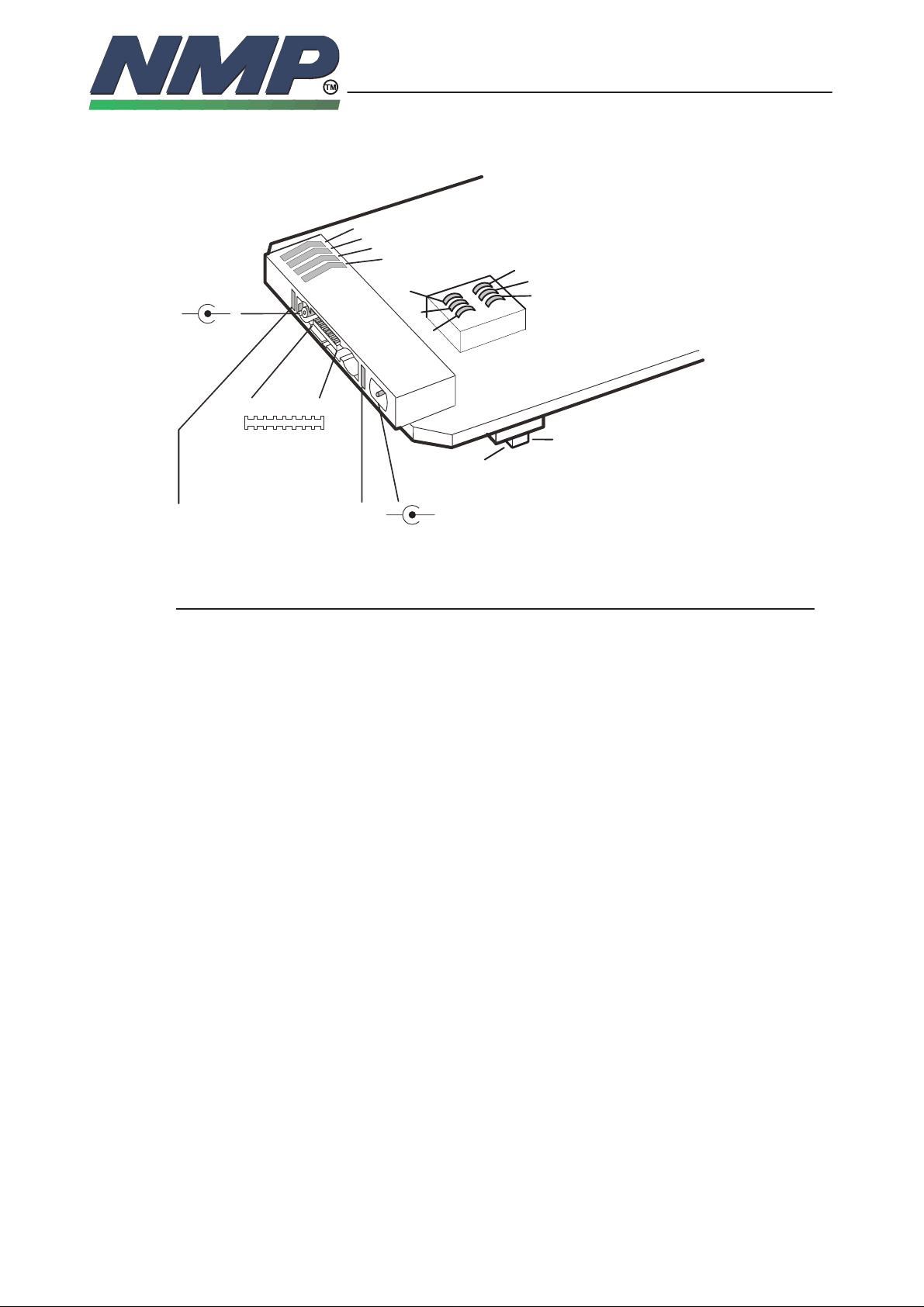
External and Internal Connectors
The system module has two connector, external bottom connector and internal
UIF module connector.
Page 4
SYSTEM MODULE GS8
NHE–3
Bottom Connector X100
Battery connector
Antenna
connector
2
43
1
16
System connector
Charging connectors
1298 OJ
Technical Documentation
4
3
X100
9
18
SIM card connector
2
1
1
2
3
2
1
6
5
4
1
21
X584
UIF module connector
8–4
Copyright Nokia Mobile Phones
S0001049
System Connector
Pin: Name: Description:
1, 9 GND Digital ground
2 MIC_JCONN External audio input from accessories or
3 AGND Analog ground for accessories.
4 TDA Transmitted DBUS data to the accessories.
5 M2BUS Serial bidirectional data and control between
6 HOOK/RXD2 HOOK indication. The phone has a 100 kΩ
7 PHFS/TXD2 Handsfree device power on/off, data to flash
8, 16 VCHAR Battery charging voltage.
10 EAR_HFPWR External audio output to accessories or
handsfree microphone. Multiplexed with
junction box connection control signal.
the handportable and accessories.
pull–up resistor.
programming device.
handsfree speaker.
11 DSYNC DBUS data bit sync clock
12 RDA DBUS received data from the accessories
13 BENA Power supply to headset adapter.
14 VF Programming voltage for FLASH.
15 DCLK DBUS data clock
Page 5

SYSTEM MODULE GS8
NHE–3
Battery Connector
Pin: Name: Description:
1 GND Ground
2 TBAT Battery temperature
3 BTYPE Battery type
4 VBATT Battery voltage
Charging Connector
Pin: Name: Description:
1 VCHAR Battery charging voltage
2 GND Ground
3 VCHAR Battery charging voltage
4 GND Ground
1298 OJ
Technical Documentation
8–5
Copyright Nokia Mobile Phones
Antenna Connector
Pin: Name: Description:
1 RF EXT External antenna signal
2 GND Ground
UIF Module Connector X584
Pin: Name: Description:
1 VL1 Logic supply voltage 4.65 V
2, 25 GND Ground
3, 30 VBATT Battery voltage
4 BACKLIGHT Backlights on/off
5 – 8 UIF(0;3) Lines for keyboard read and LCD controller
9 UIF4 Line for keyboard read and LCD drive
10 UIF5 Line for keyboard read and LCD driver
read/write strobe
data/command mode selection
11 UIF6 LCD driver chip select
12 UIF7 Busy signal from LCD driver to MCU
13 – 16 COL(0;3) Lines for keyboard read
17 UIF8 LCD driver reset
18 MICP Microphone (positive node)
Page 6

SYSTEM MODULE GS8
NHE–3
19 MICN Microphone (negative node)
20 EARP Earpiece (negative node)
21 EARN Earpiece (positive node)
22 BUZZER PWM signal buzzer control
23 XPWRON Power key (active low)
24 VA1 Analog supply voltage 4.65 V
26 MICENA Microphone bias enable
27 VIBRA Vibrating alert control
28, 29 AGND Analog ground
SIM Card Connector
Pin: Name: Description:
1 SIMCLK Clock for SIM data
1298 OJ
Technical Documentation
8–6
Copyright Nokia Mobile Phones
2 SIMRES Reset for SIM
3, 5 VSIM SIM voltage supply
4 GND Ground for SIM
6 SIMDATA Serial data for SIM
Internal Signals Between RF and ASIC
Symbol: Description: Values:
SCLK Synthesizer clock
• load impedance:
• frequency:
SDATA Synthesizer data
• load impedance:
• data rate frequency:
SENAR RX synthesizer enable
• VHF PLL contr. disabled:
• VHF PLL activated:
• current:
10 k
Ω
3.25 MHz
10 k
Ω
3.25 MHz
4.5...4.65...4.8 V
0...0.2...0.7 V
50 µA
SENAT TX synthesizer enable
• UHF PLL contr. disabled:
• UHF PLL activated:
• current:
4.5...4.65...4.8 V
0...0.2...0.7 V
50 µA
Page 7

SYSTEM MODULE GS8
NHE–3
1298 OJ
Technical Documentation
RXPWR RX supply voltage on/off
• RX supply voltage on:
• RX supply voltage off:
• current:
SYNTHPWR Supply voltage on/off
• RF regulators on:
• RF regulators off:
• current:
TXPWR TX supply voltage on/off
• TX supply voltage on:
• TX supply volatge off:
• current:
TXP TX enable
• transmitter power enable:
• transmitter power disable:
CLKIN 26 MHz clock to ASIC
8–7
Copyright Nokia Mobile Phones
4.5...4.65...4.8 V
0...0.2...0.7 V
0.5 mA
4.5...4.65...4.8 V
0...0.2...0.7 V
1.0 mA
4.5...4.65...4.8 V
0...0.2...0.7 V
0.5 mA
4.5...4.65...4.8 V
0...0.2...0.7 V
Internal Signals Between RF and RFI
Symbol: Description: Values:
AFC Automatic frequency control voltage
• voltage min/max:
• resolution:
• load impedance (dynamic):
TXC TX transmit power control voltage
• voltage range min/max:
• impedance:
TXQP,TXQN Differential TX quadrature signal
• differential voltage swing:
• d.c. level:
• load impedance:
TXIP,TXIN Differential TX inphase signal
• differential voltage swing:
• d.c. level:
• load impedance:
PDATA0 Parallel AGC data
• reduced front end gain:
• normal front end gain:
• current:
0.35...4.35 V
11 bits
10 k
Ω
0.3...4.2 V
10 k
Ω
1.15...1.2...1.25 V
PP
2.30...2.35...2.40 V
30 k
Ω
1.15...1.2...1.25 V
PP
2.30...2.35...2.40 V
30 k
Ω
4.5...4.65...4.8 V
0...0.2...0.7 V
0.1 mA
PDATA1 Parallel AGC data
• AGC 3 dB reduction:
• normal front end gain:
• current:
4.5...4.65...4.8 V
0...0.2...0.7 V
10 µA
Page 8

SYSTEM MODULE GS8
NHE–3
1298 OJ
Technical Documentation
PDATA2 Parallel AGC data
• AGC 6 dB reduction:
• normal front end gain:
• current:
PDATA3 Parallel AGC data
• AGC 12 dB reduction:
• normal front end gain:
• current:
PDATA4 Parallel AGC data
• AGC 24 dB reduction:
• normal front end gain:
• current:
PDATA5 Parallel AGC data
• AGC 12 dB reduction:
• normal front end gain:
• current:
RXQ RX quadrature signal
• output level:
• source impedance:
8–8
Copyright Nokia Mobile Phones
4.5...4.65...4.8 V
0...0.2...0.7 V
10 µA
4.5...4.65...4.8 V
0...0.2...0.7 V
10 µA
4.5...4.65...4.8 V
0...0.2...0.7 V
10 µA
4.5...4.65...4.8 V
0...0.2...0.7 V
10 µA
25 mV
470
PP
Ω
RXI RX inphase signal
• output level:
• source impedance: 470 Ω
Functional Description of Baseband Block
The purpose of the baseband module is to control the phone and process audio
signals to and from RF. The module also controls the user interface.
Technical Specifications
There are three different operation modes:
– Active mode
– Idle mode
– Power off mode
In the active state all the circuits are supplied with power and part of the mod-
ule might be in idle state.
The module is usually in the idle mode when there is no call. In the idle mode
circuits are reset, powered down and clocks are stopped or the frequency reduced.
25 mV
PP
In power off mode only the circuits needed for power up are supplied with
power.
Page 9
SYSTEM MODULE GS8
NHE–3
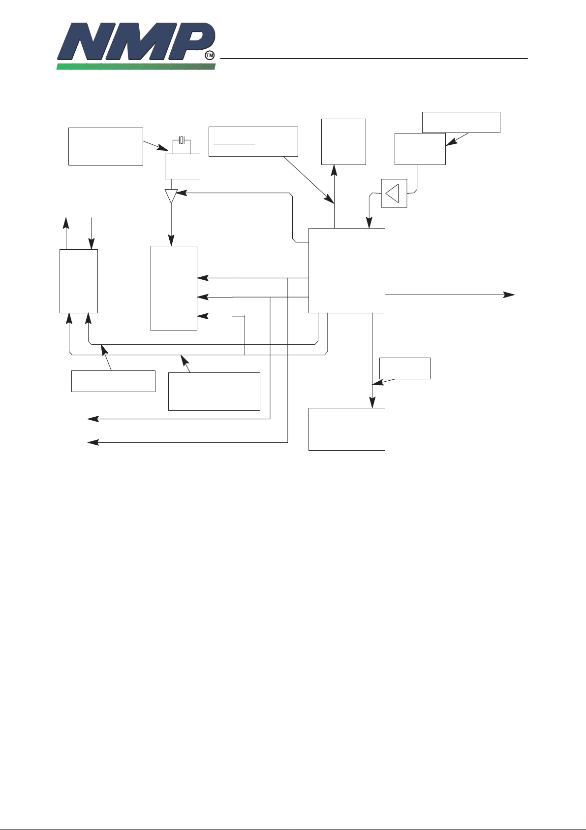
Clocking Sceme
DSP Clock
60.2 MHz
differential sine
wave
ear
mouth
AUDIO
CODEC
oscillator
DSP
1298 OJ
Technical Documentation
RFI Clock 13 MHz
Sleep Mode:
135.4kHz
enable
RFI
ASIC
8–9
Copyright Nokia Mobile Phones
RF System Clock
26 MHz
VCTCXO
SIMCLKSIMCLK
3.25 / 1.625
MHz
Codec Sync Clock
8 kHz
DBUSCLK 512kHz
DBUSSYNC 8kHz
Most of the clocks are generated from the 26 MHz VCTCXO frequency by the
ASIC:
– 26 MHz clock for the MCU. MCU‘s internal clock frequency is half of that.
– 13 MHz for the RFI. The ASIC also generates 135.4 kHz sleep mode clock
for the RFI
– 3.25 MHz clock for SIM. When there is no data transfer between the SIM
card and the HP the clock can be reduced to 1.625 MHz. Some SIM cards
also allows the clock to be stopped in that mode
– 512 kHz main clock for the codec and for the data transfer between the
DSP and the codec
– 8 kHz syncronisation clock for data transfer between the DSP and the codec
Codec Main Clock
and data Transfer
clock
512kHz
MCU Clock
26 MHz
MCU
– 512 kHz clock and 8 kHz sync. clock for the DBUS data transfer.
The DSP has its own crystal oscillator which can be turned off and on by the
ASIC. The DSP uses differential sinusoidal clock. The frequency is 60.2 MHz
The MCU generates 8 kHz clock to the codec for the control data transfer. In
the idle mode all the clocks can be stopped except 26 MHz main clock coming
from the VCTCXO.
Page 10
SYSTEM MODULE GS8
NHE–3
Reset and Power Control
reset in
DSP
1298 OJ
Technical Documentation
RFI
Reset Out
Reset Out
ASIC
Vcc
Reset in
resetreg
8–10
Copyright Nokia Mobile Phones
SIMReset
PSL+
VL1
XRES reset in
XPWRON
XPwrOff
approx 2Hz
There are three different ways to switch power on:
• Power key pressing grounds the XPWRON line. The PSL+ detects that and
switches the power on.
• Charger detection on PSL+ detects that charger is connected and switches
power on
• PSL+ will switch power on when the battery is connected. After that the MCU
will detect if power key is pressed or charger connected. If not the power will
be switched off
All devices are powered up at the same time by the PSL+. It supplies the reset
to the ASIC at power up. The ASIC starts the clocks to the DSP and the MCU.
After about 20 µs the ASIC releases the resets to MCU, RFI and DSP. MCU
and RFI reset is released after 256 13 MHz clock cycles. DSP reset release
time from DSP clock activation can be selected from 0 to 255 13MHz clock
cycles. In our case it is 255. SIM reset release time is according to GSM SIM
specifications.
XPWRON
MCU
To turn off power for the phone, the user presses the PWR key. The MCU detects this. The MCU cuts off any ongoing call, exits all tasks, acts inoperative to
the user and leaves the PSL+ watchdog without resets. After power–down
Page 11
SYSTEM MODULE GS8
NHE–3
delay, the PSL+ cuts off the supply from all circuitry. If charging is on the phone
stays on but it looks to the user like it is powered off (lights are off and the display is blank) except the charging indicator stays on.
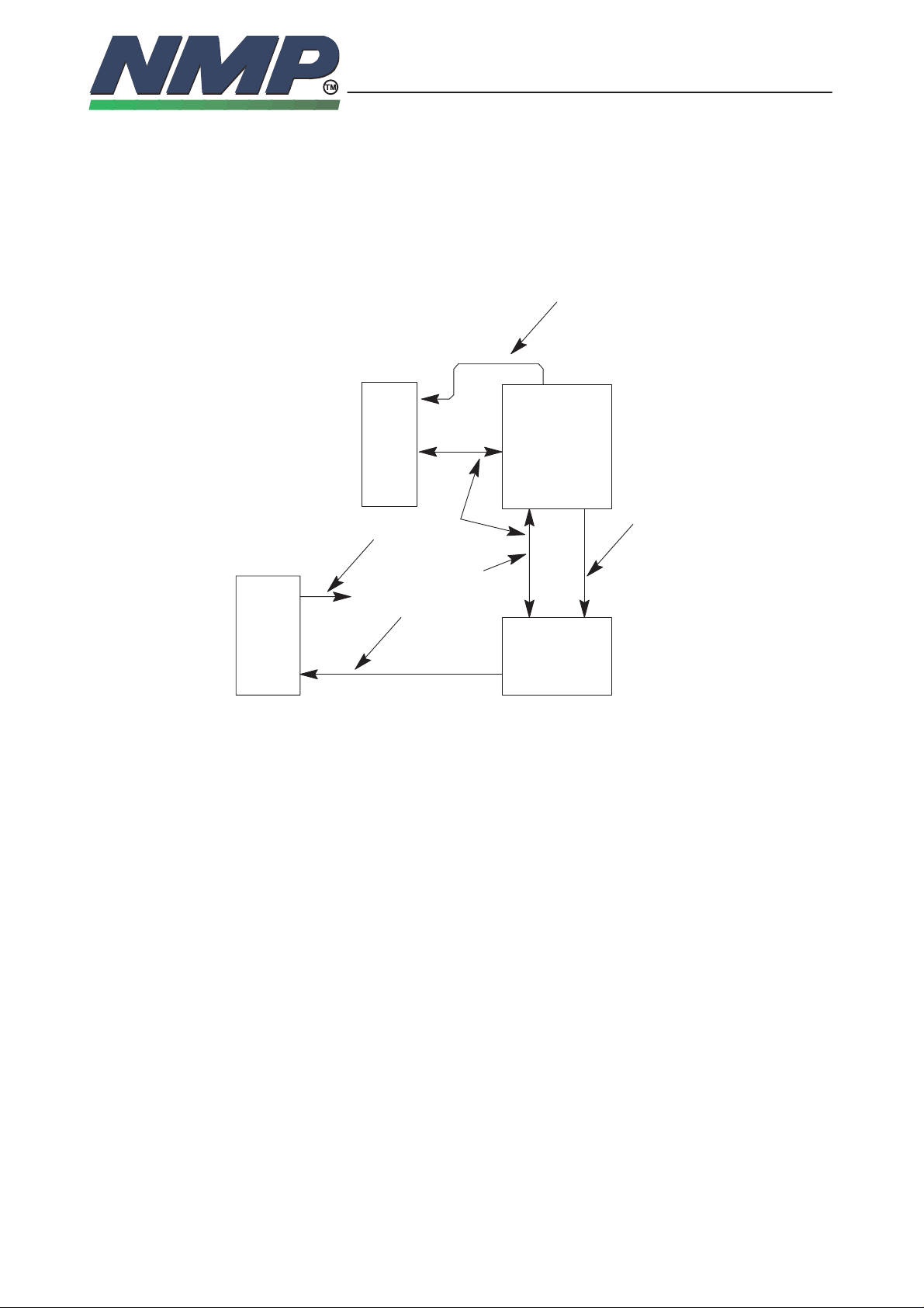
Watchdog System
1298 OJ
Technical Documentation
reset
DSP
5
1
8–11
Copyright Nokia Mobile Phones
4
ASIC
4
2
POWER
3
PSL
XPWROFF
reset
MCU
Normal operation:
1. MCU tests DSP
2. MCU updates ASIC watchdog timer (> 2Hz)
3. MCU pulses the XPWROFF input on the PSL+ (about 2Hz)
Failed operation:
4. ASIC resets MCU and DSP after about 0.5 s failure
5. PSL+ switches power off about1.5 s after the previous XPWROFF pulse
Page 12

SYSTEM MODULE GS8
NHE–3
1298 OJ
Technical Documentation
Names of Functional Blocks
Name: Function:
CTRLU Control unit for the phone
PWRU Power supply
DSPU Digital signal processing block
AUDIO Audio coding
ASIC EDSA –asic
RFI RF –baseband interface
CTRLU
The Control block contains a microcomputer unit (MCU) and three memory circuits (FLASH, SRAM, EEPROM), a 20 bit address bus and an 8 bit data bus.
Main Features of the CTRLU block:
8–12
Copyright Nokia Mobile Phones
MCU functions:
– system control
– communication control
– user interface functions
– authentication
– RF monitoring
– power up/down control
– accessory monitoring
– batttery monitoring and charging control
– self–test and production testing
– flash loading
Main Components of CTRLU
– Hitachi H8/536
H8/536 is a CMOS microcomputer unit (MCU) comprising a CPU
core and on–chip supporting modules with 16 bit architecture. The
data bus to outside world has 8 bits.
– 1024 k x 8 bit FLASH memory
– 100 ns maximum read access time.
– contains the main program code for the MCU; part of the DSP
program code locates also in FLASH.
– ASIC can address two 4 Mbit memories or one 8 Mbit memory.
Page 13

SYSTEM MODULE GS8
NHE–3
– 32 k x 8 bit SRAM memory
– 100 ns maximum read access time.
– 8 k x 8 bit EEPROM memory
– 150 ns maximum read access time.
– contains user defined information.
– there is a register bit on the ASIC which must be set before the
Input Signals of CTRLU
Name(from): Description:
VL1(PWRU) Power supply voltage for CTRLU block
VREF(PWRU) Reference voltage for MCU A/D converter
VBATDET(PWRU) Battery voltage detection
1298 OJ
Technical Documentation
write operation to the EEPROM.
8–13
Copyright Nokia Mobile Phones
VC(PWRU) Charger voltage monitoring
EROMSELX(ASIC) Chip select for the EEPROM memory
ROMSELX(ASIC) Chip select for the FLASH memory
ROM2SELX(ASIC) Chip select for the 2nd FLASH memory
RAMSELX(ASIC) Chip select for the SRAM memory
RESETX(ASIC) Reset signal for MCU
NMI(ASIC) Non–maskable interrupt request
MCUCLK(ASIC) Main clock for MCU
IRQX(ASIC) Interrup request
PCMCDO(AUDIO) Audio codec control data receiving
TRF(RF) RF module temperature detection
VF(system conn.) Programming voltage for FLASH memory
RXD2_HOOK The use of handsfree monitoring
(system conn.) FLASH programming data input on the production line
TBAT(batt.conn.) Battery temperature detection
BTYPE(batt.conn.) Battery size identification
JCON(syst.conn.) Junction box connection identification
Page 14

SYSTEM MODULE GS8
NHE–3
Output Signals of CTRLU
Name(to): Description:
XPWROFF(PWRU) Power off control, PSL+ watchdog reset
PWM(PWRU) Charger on/off control
WSTROBEX(ASIC) MCU write strobe
RSTROBEX(ASIC) MCU read strobe
MCUAD(19:0)(ASIC)20 bit MCU address bus
MBUSDET(ASIC) MBUS activity detection
PCMCLK(AUDIO) Clock for audio cedec control data transfer
PCMCDI(AUDIO) Audio codec control data transmitting
XSELPCMC(AUDIO)Chip select for audio codec
TXD2_PHFS Power on/off control for HF device, verification output
(syst.connector) of the programmed data of FLASH during programming
1298 OJ
Technical Documentation
8–14
Copyright Nokia Mobile Phones
UIF8(UIF) reset for display driver
BACKLIGHT(UIF) LCD and display backlight on/off control
BUZZER(UIF) Buzzer signal
VIBRA(UIF) Vibrating alert control
Bidirectional Signals of CTRLU
Name(to/from): Description:
MCUDA(7;0)(ASIC) MCU’s 8 bit data bus
M2BUS Asyncronous serial data bus
Page 15

SYSTEM MODULE GS8
NHE–3
Block Description of CTRLU
– MCU – memories
MCU has a 20 bits wide address bus A(19:0) and an 8 bit data bus
with memories. The address bits A(19:16) are used for chip select
decoding. The decoding is done in ESA asic.The ASIC can address
two 4 Mbit (or smaller) or one 8 Mbit flash memories. Hitachi
HD647536 processor has internal ROM and RAM memories.
On the Hitachi HD647536 internal memory map there is the following:
• 00000 – 001FF vector tables
• 00000 – 0F67F 62 kbytes internal ROM
• 0F680 – 0FE7F 2 kbytes internal RAM
• 0FE80 – 0FFFF 384 bytes registers
External memory map is the following:
1298 OJ
Technical Documentation
8–15
Copyright Nokia Mobile Phones
• 10000 – 1FFFF 32 k * 8 bytes RAM
• 20000 – 21FFF 8 k * 8 bytes EEROM
• 30000 – 3FFFF 26 * 8 bytes ASIC
• 40000 – 7FFFF 2 Mbit bytes FlashROM
• 80000 – BFFFF 4 Mbit bytes FlashROM
Chip select generation:
Chip: Page: A19: A18: A17: A16:
RAM X 0 0 0 1
EEPROM X 0 0 1 0
ASIC X 0 0 1 1
FLASH1 0 0 1 X X
FLASH1 1 0 1 X X
FLASH2 or X 1 X X X
FLASH1 if 8 Mbit
flash used
– Flash programming
In flash programming a special flash programming box and a PC is
needed. Loading is done through the bottom connector of HP; multiplexed with HOOK and PHFS line. First MCU goes to minimum
mode (MBUS command from PC or if MBUS is connected to
MIC_JCONN line in power up). Then the flash software is loaded
from PC to flash loading box. When the loading is complete flash
loading to HP can be started by MBUS command from PC to the
MCU. After that the MCU asks the test box to start flash loading to
HP.
Page 16

SYSTEM MODULE GS8
NHE–3
The box supplies 12 V programming voltage for flash and starts to
send 250 bytes data blocks to the MCU via HOOK line. The baud
rate is 406 kbit/s. The MCU calculates the check sum, sends acknowledge via PHFS line and sends the data to flash. When all the
data is loaded the HP makes reset and tells the flash loading box if
the loading was succeeded or not. Only PSL+, ASIC and MCU must
be active during the loading.
– CTRLU – PWRU
MCU controls the watchdog timer in PSL+. It sends a positive pulse
at approximately 2 Hz to XPWROFF pin of the PSL+ to keep the
power on. If MCU fails to deliver this pulse, the PSL+ will remove
power from the system. MCU controls also the charger on/off switching in the PWRU block. When power off is requested MCU leaves
PSL+ watchdog without reset. After the watchdog has elapsed PSL+
cuts off the supply voltages from the phone.
– CTRLU – ASIC
MCU and ASIC have a common 8 bit data bus and a 9 bit address
bus. A(4:0) are used for normal addressing whereas bits A(19:16)
are decoded in ASIC to chip select inputs for CTRLU memories.
ASIC controls the main clock, main reset and interrupts to MCU. The
internal clock of MCU is half the MCUCLK clock speed. RESETX resets everything in MCU except the contents of the RAM. IRQX is
general purpose interrupt request line from ASIC. After IRQX request
the interrupt register of asic is read to find out the reason for interrupt. NMI interrupt is used only to wake up MCU from software
standby mode.
1298 OJ
Technical Documentation
8–16
Copyright Nokia Mobile Phones
– CTRLU – DSPU
MCU and DSP communicate through ASIC. ASIC has MCU mailbox
and DSP mailbox. MCU writes data to DSP mailbox where DSP can
only read the incoming data. In MCU mailbox data transfer direction
is opposite. When power is switched on the MCU loads data from
the flash memory to DSP‘s external memory through this mailbox.
– CTRLU – AUDIO
When the the chip select signal XSELPCMC goes low, MCU writes
or reads control data to or from the speech codec registers at the
rate defined by PCMCLK. PCMCDI is an output data line from MCU
to codec and PCMCDO is an input data line from codec to MCU.
Page 17

SYSTEM MODULE GS8
NHE–3
1298 OJ
Technical Documentation
– CTRLU – RF/BATTERY monitoring
MCU has internal 8 channel 10 bit AD converter. Following signals
are used to monitor battery, charging and RF:
• BTYPE; battery size
• TBAT; battery temperature
• VBATDET; battery voltage
• VC; charging voltage
• TRF; RF temperature
– CTRLU – keyboard and LCD driver interface
MCU and user interface communication is controlled through ASIC.
– CTRLU – ACCESSORIES
M2BUS is used to control external accessories. This interface can be
used also to factory testing and service and maintenance purposes.
There are also some control and indication signals for the accessories:
8–17
Copyright Nokia Mobile Phones
• PHFS is used to turn power on to HF accessories
• JCONN is used to indicate that junction box is connected. Phone
can also enter minimum mode when M2BUS is connected to
MIC_JCONN line.
• HOOK is used to indicate accessories hook state
Page 18

SYSTEM MODULE GS8
NHE–3
PWRU
The power block creates the supply voltages for the baseband block and contains the charging electronics.
Main Components of PWRU
– PSL + ASIC
Generates the voltages, has power switch, charger and battery
detection and watchdog.
– Transistor BCP69–25 and schottky STPS340U
The charging current is passed through these components.
– Transistor BCX51 and BCP69–25
VL regulators of PSL+ external output transistors.
Input Signals of PWRU
1298 OJ
Technical Documentation
8–18
Copyright Nokia Mobile Phones
Name(from): Description:
XPWRON(UIF) PWR on swith
XPWROFF(CTRLU) Power off control
VBATT(batt.conn.) Battery voltage
PWM(CTRLU) Charger on/off control
VCHAR(syst.conn.) Charging voltage
Output Signals of PWRU
Name(from): Description:
XRES(ASIC) Master reset
VL1(CTRLU,ASIC, Logic supply voltage, max 150 mA
RFI,UIF)
VL2(DSPU) Logic supply voltage, max 150 mA
VA1(AUDIO,UIF) Analog supply voltage, max 40 mA
VA2(RFI) Analog supply voltage, max 80 mA
VREF(CTRLU,RF) Reference voltage 4.65 V ±2 %, max 5 mA
VBATDEF(CTRLU) Switched VBATT divided by 2
VC(CTRLU) Attenuator VCHAR
Page 19

SYSTEM MODULE GS8
NHE–3
Block Description of PWRU
The PSL+ IC produces the supply voltages:
Name: Description:
2 * VL 150 mA for logic
VA1 40 mA for audios
VA2 80 mA for RFI
VREF 5 mA reference
In addition, It has internal watchdog, voltage detection and charger detection
functions. The watchdog will cut off output voltages if it is not reset once in every 1.5 〈±0.75) second. The voltage detector resets the phone if the battery
voltage falls below 4.8 V (±0.2 V). The charger detection starts the phone if it is
in power–off state when the charging voltage is applied.
The charging electronics is controlled by the MCU. When the charging voltage
is applied to the phone and the phone is powered up, the MCU detects it and
starts controlling the charging. If MCU detects too high charging voltage (over
14 volts) or current (over 78 A/D bit difference between VC and VBATDET) it
will cut off the charging. The phone will accept charging voltages from 5 to 14
volts.
1298 OJ
Technical Documentation
8–19
Copyright Nokia Mobile Phones
If the phone is in power–off state, the PSL+ will detect the charging voltage and
start the phone. If the battery voltage is high enough the reset will be released
and the MCU will start controlling charging.
If the battery voltage is too low the phone stays in reset state and charging control circuitry will pass small charging current to the battery. When the battery
voltage has reached 5.25 V (±0.2 V) the reset will be removed and the MCU
starts controlling the charging.
MCU controls the charging with pulse width modulation output.
Charging voltage is limited by hardware in normal operation to 8.9 V and during
a call to 7.6 V.
Battery and charging voltages are calibrated in production; 6 V is fed to the battery and charger pin and the MCU‘s A/D converter values are stored to EEPROM
Page 20

SYSTEM MODULE GS8
NHE–3
DSPU
1298 OJ
Technical Documentation
Copyright Nokia Mobile Phones
Main interfaces of the DSP:
– MCU via ASIC mailbox
– ASIC
– audio codec
– data bus interface (DBUS) for accessories
– digital audio interface (DAI) for type approval measurements
Main features of the DSP block:
– speech processing
– speech coding/decoding
– RPE–LTP–LPC (Regular pulse excitation long term
prediction linear predictive coding)
– voice activity detection (VAD) for discontinuous transmission
(DTX)
8–20
– comfort noise generation during silence
– acoustic echo cancellation
– channel coding and transmission
– block coding (with ASIC)
– convolutional coding
– interleaving
– ciphering (with ASIC)
– burst building and writing it to ASIC
– Reception
– reading the A/D conversion results from ASIC
– impulse response calculation
– matched filtering
– bit detection (with Viterbi on ASIC)
– deinterleaving of soft decisions
– convolutional decoding (with Viterbi)
– block decoding (with ASIC)
– Adjacent cell monitoring
– signal strenght measurements
– neighbour timing measurements
– neighbour parameter reception
Page 21

SYSTEM MODULE GS8
NHE–3
– control functions
– RF controls
– frame structure control
ASIC)
– test functions
– functions for RF measurements
– debugging functions for product development
1298 OJ
Technical Documentation
Copyright Nokia Mobile Phones
– synthesizer control
– power ramp programming
– automatic gain control (AGC)
– automatic frequency control (AFC)
– controlling the operations during a TDMA frame (with
– controlling the multiframe structure
– channel configuration control
8–21
Main Components of DSPU
– AT&T DSP 1616–X11
– Digital signal processor with 12kword internal ROM
– Two 32 k *8 70 ns SRAMs for DSP external memory
– 60.2 MHz crystal oscillator to generate differential small signal clock for the
DSP
Input Signals of DSPU
Name(from): Description:
VL2(PWRU) Logic supply voltage, max 150 mA
DSPCLKEN(ASIC) Clock enable for DSP clock oscillator circuit
DSP1RSTX(ASIC) Reset for the DSP
PCMDATRCLKX PCM data input clock
(ASIC) DBUS data output clock
CODEC_CLK PCM data output clock
PCMOUT(AUDIO) Received audio in PCM format
DBUSCLK DBUS data output clock
DBUSSYNC DBUS data bit sync clock
RDA DBUS received data
INT0, INT1(ASIC) Interrupts for the DSP
Page 22

SYSTEM MODULE GS8
NHE–3
PCMCOSYCLKX PCM data bit sync clock
(ASIC)
Output Signals of DSPU
Name(to): Description:
PCMIN(AUDIO) Transmitted audio in PCM format
IOX(ASIC) I/O enable, indicates access to DSP address space
RWX(ASIC) Read/write X
DSPAD(16;9)(ASIC) Address bus and control signals
DBUSDET(ASIC) DBUS activity detection
Bidirectional Signals of DSPU
Name(from/to): Description:
1298 OJ
Technical Documentation
8–22
Copyright Nokia Mobile Phones
DSPDA(15;0)(ASIC) 16 bit data bus
Block Description of DSPU
Control unit communicates with the DSP circuitry trough a mailbox in the ESA
ASIC. The software for the external memories are loaded through this mailbox
in start up.
The DSP includes two serial busses. One is used for speech data transfer between the DSP and the codec. The other is used as an external data bus and it
is connected to the bottom connector. This bus can be used by data accessories and also as a digital audio interface (DAI) in audio type approval measurements. The clocks (512 kHz main clock and 8 kHz sync. clock) are generated
by the ASIC.
In transmit mode the DSP codes the speech and routes the resulting transmit
slots to the ESA. The ESA ASIC controls timing, and at specified intervals
sends these bits to the RFI for DA conversion.
In digital receive mode the RFI AD converts the IF signal from the RF unit under the control of the ESA. The DSP controls the ESA and receives the converted bits. After channel and speech decoding, bits are converted into an analog signal in the PCM codec, routed and fed to the earpiece.
The DSP controls the RF through the ESA ASIC, where all necessary timing
functions are implemented, and control I/O lines are provided eg. for synte
loading.
DSP emulator can be connected to DSP pins TCK, TMS, TDO, TDI, GND and
VDD.
Page 23

SYSTEM MODULE GS8
NHE–3
AUDIO
The AUDIO block consists of an audio codec with some peripheral components. The codec contains microphone and earpiece amplifier and all the necessary switches for routing. The codec is controlled by the MCU. The PCM data
comes from and goes to the DSP.
Main Components of AUDIO
– Audio codec ST5080
Includes e.g. PCM codec, audio routing switches, microphone and
earpiece amplifiers for 2 connections (internal and external devices)
and DTMF generator.
Input Signals of AUDIO
Name(from): Description:
1298 OJ
Technical Documentation
8–23
Copyright Nokia Mobile Phones
VA1(PWRU) Analog supply voltagee, max 40 mA
PCMIN(DSPU) Received audio in PCM format
SYNC(ASIC) 8 kHz frame sync
CODEC_CLK(ASIC) 512 kHz codec main clock
PCMCDI(CTRLU) Audio codec control data
PCMCLK(CTRLU) Clock for audio codec control data transfer
XSELPCMC Audio codec chip select
(CTRLU)
HFMIC(syst.conn.) External microphone
MICN,MICP(UIF) Differential microphone signal
Output Signals of AUDIO
Name(to): Description:
PCMOUT(DSPU) Transmitted audio in PCM format
PCMCDO(CTRLU) Audio codec control data
MICENA(UIF) Microphone enable
EXTEAR(syst.conn.) External received audio
EARN,EARP(UIF) Internal received audio
JCONN(CTRLU) Junction box connected signal (multiplexed with HFMIC)
Page 24

SYSTEM MODULE GS8
NHE–3
Block Description of AUDIO
The codec has two microphone inputs and two earphone outputs. Handportable and external audios can therefore be connected directly to the codec. The
codec has internal switches to select which input or output is used. It also has
microphone amplifier and earphone attenuator. Input/output selection and amplification/attenuation can be done with codec register settings.The register
control is done by the MCU.
Handportable microphone and earphone (located on the flex) are connected
directly to the codec‘s differential input and output. External audios are connected single sided. There is 21 dB attenuation in the external microphone line
before the codec to prevent clipping.
Microphone signal is routed to the microphone amplifier. After that it is fed to
the band pass filter and then to the A/D converter. After the conversion the digital speech is sent to the DSP.
Digital downlink signal from the DSP is fed to the D/A converted. After the converter there is low pass filter and attenuator before the earphone output. All
these are inside the codec. The ASIC generates the 512 kHz and 8 kHz clocks
for the codec and data transmission between the codec and the DSP.
1298 OJ
Technical Documentation
8–24
Copyright Nokia Mobile Phones
The audio codec communicates with the DSP (analog speech) through an SIO
(signals: PCMIN, SYNC, CODEC_CLK and PCMOUT) . The MCU controls the
audio codec function through a separate serial bus (signals: PCMCDO,
PCMCDI, PCMCLK and XSELPCMC).
The codec generates DTMF tones (key beeps) to the earphone and in HF
mode to the external speaker. In portable mode the MCU generates ringing
tones and also some warning tones to the buzzer. In HF mode they are generated by the codec and driven to the external speaker line. Some tones come
also from the network.
One codec output pin is used to switch on/off the microphone bias circuit on the
flex.
External microphone line is used also to detect if junction box is connected to
the bottom connector. Microphone signal is therefore routed to the MCU A/D
converter.
Also external earphone signal is multiplexed. 100 kohm pull down resistor is
used to turn power on to the HF accessories.
Page 25

SYSTEM MODULE GS8
NHE–3
ASIC
The ASIC takes care of the following functions:
– interface between MCU and UIF
– interface between MCU, DSP and RFI
– hardware accelerator functions to DSP
– clock generation and disable/enable
– RF controls
– UIF interface
– timers
– M2BUS interface
– SIM interface
Main Components of ASIC
1298 OJ
Technical Documentation
8–25
Copyright Nokia Mobile Phones
– ESA ASIC
– RFC buffer
Inverter buffer stage is used as a buffer for VCTCXO clock.
Input Signals of ASIC
Name(from): Description:
VL1(PWRU) Logic supply voltage ax 150 mA
IOX(DSPU) I/O enable, indicates access to DSP address space
RWX(DSPU) Read/write X
WSTROBEX MCU’s write strobe
(CTRLU)
RSTROBEX MCU’s read strobe
(CTRLU)
RFC(RF) Reference clock from VCTCXO
XRES(PWRU) Master reset
DSPAD(16;0)(DSPU)Address bus and control signals
MCUAD(19;16,4;0) MCU’s address bus
(CTRLU)
DAX(RFI) Data acknowledge
MBUSDET(CTRLU) MBUS activity detection
DBUSDET(DSPU) DBUS activity detection
Page 26

SYSTEM MODULE GS8
NHE–3
Output Signals of ASIC
Name(to): Description:
INT0,INT1(DSPU) Interrupts for DSP
NMI(CTRLU) Not maskable interrup request
IRQX(CTRLU) Interrupt request
RESETX Master (power up) reset
(CTRLU,RFI)
DSP1RSTX(DSPU) Reset for the DSP
WRX(RFI) Write strobe
RDX(RFI) Read strobe
RFIAD(3;0)(RFI) RFI address bus
SCLK(RF) Synthesizer load clock
SDATA(RF) Synthesizer load data
1298 OJ
Technical Documentation
8–26
Copyright Nokia Mobile Phones
SENAR(RF) Receiver synthesizer enable
SENAT(RF) Transmit synthesizer enable
RXPWR(RF) RX circuitry power enable
TXPWR(RF) TX circuitry power enable
SYNTHPWR(RF) Synthesizer circuitry power enable
TXP(RF) Transmit enable
MCUCLK(CTRLU) Main clock for MCU
DSPCLKEN(DSPU) DSP clock circuit enable
RFICLK(RFI) RFI master clock
RFI2CLK(RFI) RFI sleep clock
CODEC_CLK PCM data clock
(DSPU,AUDIO)
PCMDATRCLKX Inverted PCM data clock, used as input clock for
(DSPU) codec and DBUS interface
SYNC(AUDIO) Bit sync clock
PCMCOSYCLKX Bit sync clock, inverted
(DSPU)
DCLK(DSPU) DBUS data clock
DSYNC(DSPU) DBUS bit sync clock
ROMSELX(CTRLU) Chip select for the FLASH memory
ROM2SELX Chip select for the second FLASH memory
(CTRLU)
Page 27

SYSTEM MODULE GS8
NHE–3
EROMSELX Chip select for the EEPROM memory
(CTRLU)
RAMSELX(CTRLU) Chip select for the SRAM memory
COL(3;0)(UIF) Lines for keyboard column write
BENA(system con.) Power supply for headset adapter
Bidirectional Signals of ASIC
Name(from/to): Description:
DSPDA(15;0) 16 bit data bus
(DSPU)
MCUDA(7;0) MCU’s 8 bit data bus
(CTRLU)
RFIDA(11;0)(RFI) 12 bit data bus
UIF(6;0)(UIF) LCD controller control and keyboard read bus
1298 OJ
Technical Documentation
8–27
Copyright Nokia Mobile Phones
Block Description of ASIC
PSL+ supplies the reset to the ASIC at power up. The ASIC starts the clocks to
the DSP and the MCU. After about 20 µS the ASIC releases the resets to all
circuitry. MCU and RFI reset is released after 256 13 MHz clock cycles. DSP
reset release time from DSP clock activation can be selected from 0 to 255
13MHz clock cycles. In our case 255 is selected. SIM reset release time is according to GSM SIM specifications.
The RFC buffer buffers the 26 MHz clock from theVCTCXO to the ASIC. In the
ASIC the clock is further buffered and divided for the MCU, RFI, SIM. It also
generates main and sync clocks for audio codec, DSP‘s SIOs and DBUS. The
clock outputs can be disabled in order to save current when the clock is not
needed. Also the DSP oscillator can be stopped by the ASIC.
Interface to the MCU is done with 8 bit data bus ,5 bit lower address bus, 4 bit
upper address bus, RSTRBEX, WSTROBEX, IRQX and NMI. ASIC is in the
same memory space as MCU memories. The ASIC generates chip selects
from the address bits A16–19. There is also M2BUS detector and netfree
counter on the ASIC. Netfree interrupt IRQX occurs if no activity is detected in
M2BUS in about 3ms. NMI is used to wake up the MCU from sleep mode.
MCU and DSP communicate through ASIC. ASIC has an MCU mailbox and a
DSP mailbox. MCU writes data to DSP mailbox where DSP can only read the
incoming data. In MCU mailbox the data transfer direction is the opposite. The
size of the mailbox is 64 * 8 bit.
MCU and User Interface (keyboard and display) communication is controlled
through the ASIC. COL(0–4) are used as column lines in keyboard. UIF(0–5)
are used as row lines. They are also multiplexed with display driver control signals.
Page 28

SYSTEM MODULE GS8
NHE–3
1298 OJ
Technical Documentation
Copyright Nokia Mobile Phones
8–28
When a key is pressed the ASIC gets a reset from row and starts scanning.
One column at the time is written to low and rows are used to read which key it
was. Row lines and UIF6–7 are used for display driver control. UIF(0–3) are
used as 4 bit parallel data bus for the LCD driver. UIF4 is used as read/write
strobe, UIF5 to select data or instruction register and UIF6 as chip select. UIF7
is busy line from LCD driver to MCU.
The SIM interface is the electrical interface between the smart card used in the
GSM and PCN applications and the MCU via the ASIC. ASIC converts the serial data received from the SIM to parallel data for MCU and converts parallel
data from MCU to serial mode for the card. The SIM interface also takes care
of the power up and down procedure to the card, frame and parity error checking. The communication between card and ASIC is asyncronous and half duplex.Four signals are used between the ASIC and the SIM card: SIMDATA,
SIMCLK, SIMRESET and VSIM. The clock frequency is 3.25 MHz. When there
is no data transfer between the SIM card and the HP the clock can be reduced
to 1.625 MHz. Some SIM cards also allows the clock to be stopped in that
mode. Supply voltage VSIM can be switched off by the ASIC. The supply voltage is 4.65 V. The carddetect input on the ASIC is connected to BTYPE pin and
when the battery is removed the ASIC will drive the SIM down.
The interface to the DSP is done using 6 bit address bus, 16 bit data bus, IOX
and RWX lines. Data bus is latched using IOX, address bus is not. The ASIC
also generates interrupt INT0 when an edge occurs in DBUS line (if the mask
bit is off). INT1 is used as RX interrupt and as MFI modulator interrupt to the
DSP.
Viterbi is used to perform GSM/PCN convolutional decoding and bit detection
according to viterbi algorithm. It can be controlled and accessed thoroughly by
the DSP.
Coder is used to perform block encoding, decoding, and ciphering according to
GSM algorithm A5.
The ASIC takes care of the interface between the DSP and the RFI: TX modulator, RX filter, TX and RX sample buffers and controlling state machine. The
interface to RFI is done using 12 bit data bus, 4 bit address bus, RDX and
WRX. There is data acknowledge (DAX) from RFI to ASIC. Also in this block
are the serial RF synthesizer interface (SCLK, SDAT) and the digital RF control
signals (RXPWR, TXPWR, TXP, SYNTHPWR)
Page 29

SYSTEM MODULE GS8
NHE–3
RFI
The RFI block consists of the RFI ASIC and its reference voltage generator.
This block is an interface between the RF and baseband sections. The RFI
block has the following functions:
– IF receiving and A/D conversion
– I/Q separation
– I– and Q–transmit and D/A conversion
– AFC D/A
– TXC
– digital AGC
Main Components of RFI
– RFI ASIC
– 4.096 V external voltage reference LM4040 for RFI
1298 OJ
Technical Documentation
8–29
Copyright Nokia Mobile Phones
Input Signals of RFI
Name(from): Description:
VL1(PWRU) Logic supply voltage, max 150 mA
VA2(PWRU) Analog supply voltage, max 80 mA
RESETX(PWRU) Master (power up) reset
RFIAD(3;0)(ASIC) RFI address bus
RDX(ASIC) Read strobe
WRX(ASIC) Write strobe
RFICLK(ASIC) RFI master clock
RFI2CLK(ASIC) RFI sleep clock
Output Signals of RFI
Name(to): Description:
DAX(ASIC) Data acknowledge
AFC(RF) Automatic frequency control voltage
TXC(RF) TX transmit power control voltage
TXQP,TXQN(RF) Differential TX quadrature signal
TXIP,TXIN(RF) Differential TX inphase signal
PDATA(5;0)(RF) Parallel AGC data
Page 30

SYSTEM MODULE GS8
NHE–3
RXQ(RF) RX quadrature signal
RXI(RF) RX inphase signal
Bidiractional Signals of RFI
Name(to): Description:
RFIDA(11;0)(ASIC) 12 bit data bus
Block Description of RFI
The RFI provides A/D conversion of the in–phase (RXI) and quadrature (RXQ)
signals in receive path. It has 12 bit sigma–delta A/D converters and the sample rate is 541.667 kHz.
Analog transmit path includes 8 bit D/A converters to generate the in–phase
(TXI) and quadrature (TXQ) signals. RFI has differential outputs for TXI and
TXQ. The sample rate is 1.0833 MHz.
There is 11 bit D/A converter for automatic frequency correction. The sample
rate is 1.3542 kHz.
1298 OJ
Technical Documentation
8–30
Copyright Nokia Mobile Phones
Power ramp is done with 10 bit D/A converter. The sample frequency is 1.0833
MHz.
Digital AGC control is done with PDATA outputs.
The RFI has 12 bit data bus to the ASIC. The registers in the RFI are accessed
using 4 address bits. Control and clock signals are coming from the ASIC.
The RFI has external 4.096 V voltage reference.
Page 31

SYSTEM MODULE GS8
NHE–3
1298 OJ
Technical Documentation
Functional Description of RF block
The RF block carries out all the RF functions of the transceiver. The RF block
works in GSM system.
Regulators
There are two regulators in the RF unit. The first regulator is used for the synthesizers and the second is used for the other RF circuits. The regulators regulate the battery voltage to the fixed 4.75 V level. The regulator circuitry contains several switches. The receiver, synthesizer and transmitter circuits can
therefore be switched ON and OFF separately. Switching sequence timing depends on the operation mode of the phone.
Power Distribution
All currents in the power distribution diagram are peak currents. Activity percentages in SPEECH–mode are 24.6 % for RXPWR , 8.1 % for TXPWR and
100 % for SYNTHPWR. In IDLE mode activities are 0.4 %, 0.0 % and 1.77 %
respectively. The currents of each block are controlled independently and for
example TXPWR and RXPWR are not on at the same time.
8–31
Copyright Nokia Mobile Phones
Current consumption values in this figure are peak and average values respectively
Battery
5.3...9 V
Regulator
49 mA 52/12.8 mA 69/10.9 mA
UHF PLL
VHF PLL
Buffers
RF LNAs
IF amplifiers
Mixers
AGC amplifiers
Regulator
4.75 V4.75 V
Modulator
TX buffers
Power control
VCTCXO
Power
amplifier
2 mA
1500/200 mA
VREF
SYNTHPWR
TXP
TXPWR
RXPWR
Page 32

SYSTEM MODULE GS8
NHE–3
Current Consumption
In the following table can be seen the RF current consumption with different
statues of control signals. The VCTCXO current is not included in the results.
SYNTHPWR:RXPWR: TXPWR: TXP: Typ. load current: Notes:
L L L L 0.1 mA Leakage current
H L L L 49 mA Synthesizer active
H H L L 101 mA Reception
H L H L 118 mA TX active
H L H H 1618 mA Transmission
Receiver
The received RF signal from the antenna is fed via duplex filter to the receiver
unit. The signal is amplified by a discrete low noise preamplifier. The gain of the
amplifier is controlled by the AGC1 control line. The nominal gain of 15 dB is
reduced in the strong field condition by about 34 dB. After the preamplifier the
signal is filtered by a SAW RF filter. The filter rejects spurious signals coming
from the antenna and spurious emissions coming from the receiver unit.
1298 OJ
Technical Documentation
8–32
Copyright Nokia Mobile Phones
The filtered signal is fed to the receiver integrated circuit PMB2403 V.1.4. In this
circuit the RF signal is converted down in the first mixer. The local signal comes
from the VCO. The first intermediate frequency is 71 MHz.
After the mixer the IF signal is filtered by an SAW IF filter. The filter rejects adjacent channel signals, intermodulating signals and the second IF image signal.
After filtering the signal is amplified by the AGC amplifier. The maximum usable
AGC gain depends on the rejection of the unwanted signals in the SAW IF filter.
The amplifier gain is controlled by digital control signals brought from the RF
interface circuit RFI.
The amplified IF signal is down converted in the second mixer of the IC. The
second local signal is generated in the receiver IC. The second intermediate
frequency is 13 MHz. After the down conversion the second IF signal is amplified and fed out from the RX IC.
The second IF signal is filtered by a ceramic filter. The filter rejects signals of
the adjacent channels. After the filtering the signal is amplified and then it goes
to the RFI circuit. The RFI circuit demodulates the 13 MHz IF signal by using a
sampling technique and generates the I and Q signals which are fed to the signal processing units.
Transmitter
The modulated signal from the modulator is amplified by a discrete buffer. The
amplified TX signal is fed to the power amplifier hybrid IC. The power amplifier
amplifies the signal to the predetermined output level. The output signal is filtered by the duplex filter and after that it is fed to the antenna.
Page 33

SYSTEM MODULE GS8
NHE–3
The power control circuit adjusts the output power of the PA IC to the desired
level. The analog control signal, which has a raised cosine form, comes from
the RFI. This signal controls the output power and the shape of the transmission pulse. The feedback signal is taken from the directional coupler which is
connected to the output port of the PA IC.
The modulation is done at the final TX frequency (890...915 MHz). The modulator IC, PMB2200S, generates two signals with a 90 degree phase shift from
the input signal. These signals are used in the I and Q mixers. The TX I and Q
signals are generated in the RFI and fed to the mixers. After mixing the signals
are combined and the result is a GMSK modulated signal, which is amplified.
The output signal of the modulator is filtered by a SAW RF filter before it is fed
to the transmitter.
Synthesizer
The stable frequency for the synthesizers and baseband circuits is the voltage
controlled temperature compensated crystal oscillator, VCTCXO signal. The
frequency of the VCTCXO has been selected to be 26 MHz. The frequency of
the oscillator is controlled by AFC voltage brought from the RFI circuit.
1298 OJ
Technical Documentation
8–33
Copyright Nokia Mobile Phones
The amplified signal of the voltage controlled oscillator is used for the first local
signal and for the up–conversion. The signal is also divided by a dual modulus
divider (64/65), PMB2312 or SA701D, and fed to the synthesizer IC, PMB2306.
The synthesizer IC has programmable dividers and a phase detector. By using
the VCTCXO signal as a frequency reference, the synthesizer locks the VCO
signal to the predetermined frequency by controlling the VCO‘s control voltage.
The frequency range of the UHF VCO is 1006 to 1031 MHz.
The VHF VCO signal divided by four is used as the second local signal for the
receiver and the signal divided by two is used for the synthesizer and for the
up–conversion. The VCO works at a fixed frequency which is controlled by the
second synthesizer loop. This synthesizer doesn’t need a prescaler, because
the frequency is low enough for the synthesizer. The frequency of the VHF
VCO is 232 MHz and the signal divided by four is 58 MHz.
The transmitter signal is generated in the passive mixer. The UHF VCO signal
and the VHF VCO signal divided by two are mixed and the mixing product is
filtered by an RF filter and fed to the modulator IC, PMB2200S.
Page 34

SYSTEM MODULE GS8
NHE–3
1298 OJ
Technical Documentation
Block Diagram of Baseband
32K x 16
SRAM
ear
PCM
CODEC
mic
sio
DBUS
A14:0,
D15:0
sio
DSP
ext
sio
mem
A5:0,
D15:0
RFI
12 bit parallel +
8 x control
ASIC
8–34
Copyright Nokia Mobile Phones
RF
UIF–module
LCD
DRIVER
LCD
LCD
PSL+
CHRGR
FLASH
LOAD
M2 BUS
Interface
A4:0, A19:16, D7:0
A19:0,D7:0
io ext mem
io
sio
sio
MCU
sio
A12:0,D7:0
E2PROM
8K X 8
A17:0,D7:0
1024K x 8
FLASH
A14:0,D7:0
32K x 8
SRAM
Page 35

71 MHz
Block Diagram of RF
6
AGC CONT.
4
PMB2403S
13 MHZ
SWITCH
EXT . ANTENNA
POWER
CONTROL
AGC
AMPLIFIER
1006...1031 MHz 232 MHz
UHF
VCO
DIV
64/65
PMB2306
UHF
PLL
DIV
2
VHF
VCO
PMB2200S
I/Q
MODULATOR
VHF
PLL
DIV
2
PMB2306
PLL
REGUL.
RF
REGUL.
VCTCXO
26 MHZ
3
4
2
2
2
RXI
RXQ
VBAT
DC CONT.
VREF
AFC
SYS.CLOCK
PLL CONT.
TX CONT.
TXI
TXQ
SYSTEM MODULE GS8
1298 OJ
Technical Documentation
Copyright Nokia Mobile Phones
NHE–3
8–35
Page 36

SYSTEM MODULE GS8
NHE–3
1298 OJ
Technical Documentation
Power Distribution Diagram
PSL+
VBATT
VCHAR
VL1
VL2
VA1
VA2
VREF
VA2 VL1
RFI
8–36
Copyright Nokia Mobile Phones
VBATT VREF
RF
VL2
32Kx16
SRAM
VA1
PCM
CODEC
DSP
VL2
VL1
ASIC
VREF VL1
MCU
MCU
VA1
VL1
VL1
E2PROM
8K x 8
UIF–module
UIF–module
LCD Driver
VL1
512K x 8
FLASH
VBATT
LCD
LCD
VL1
32K x 8
SRAM
Page 37

SYSTEM MODULE GS8
NHE–3
1298 OJ
Technical Documentation
Copyright Nokia Mobile Phones
Connections between System and RF Blocks
8–37
Page 38

SYSTEM MODULE GS8
NHE–3
1298 OJ
Technical Documentation
Copyright Nokia Mobile Phones
Parts List of GS8 (for 8 Mb Flash)
Code 0200382 EDMS issue 9.9
ITEM CODE DESCRIPTION VALUE TYPE
R070 1430788 Chip resistor 22 k 5 % 0.063 W 0402
R071 1430794 Chip resistor 39 k 5 % 0.063 W 0402
R072 1430754 Chip resistor 1.0 k 5 % 0.063 W 0402
R073 1430764 Chip resistor 3.3 k 5 % 0.063 W 0402
R074 1430730 Chip resistor 150 5 % 0.063 W 0402
R075 1430804 Chip resistor 100 k 5 % 0.063 W 0402
R076 1430744 Chip resistor 470 5 % 0.063 W 0402
R077 1430796 Chip resistor 47 k 5 % 0.063 W 0402
R078 1430796 Chip resistor 47 k 5 % 0.063 W 0402
R079 1430804 Chip resistor 100 k 5 % 0.063 W 0402
R110 1430842 Chip resistor 680 k 1 % 0.063 W 0402
R111 1430840 Chip resistor 220 k 1 % 0.063 W 0402
R112 1430804 Chip resistor 100 k 5 % 0.063 W 0402
R113 1430804 Chip resistor 100 k 5 % 0.063 W 0402
R114 1430732 Chip resistor 180 5 % 0.063 W 0402
R140 1430792 Chip resistor 33 k 5 % 0.063 W 0402
R141 1430788 Chip resistor 22 k 5 % 0.063 W 0402
R142 1430778 Chip resistor 10 k 5 % 0.063 W 0402
R143 1430764 Chip resistor 3.3 k 5 % 0.063 W 0402
R144 1430764 Chip resistor 3.3 k 5 % 0.063 W 0402
R145 1430732 Chip resistor 180 5 % 0.063 W 0402
R146 1430846 Chip resistor 2.7 k 1 % 0.063 W 0402
R147 1430844 Chip resistor 3.9 k 1 % 0.063 W 0402
R148 1430762 Chip resistor 2.2 k 5 % 0.063 W 0402
R149 1430762 Chip resistor 2.2 k 5 % 0.063 W 0402
R150 1430778 Chip resistor 10 k 5 % 0.063 W 0402
R151 1430804 Chip resistor 100 k 5 % 0.063 W 0402
R152 1430778 Chip resistor 10 k 5 % 0.063 W 0402
R160 1430726 Chip resistor 100 5 % 0.063 W 0402
R161 1430770 Chip resistor 4.7 k 5 % 0.063 W 0402
R162 1430778 Chip resistor 10 k 5 % 0.063 W 0402
R163 1430726 Chip resistor 100 5 % 0.063 W 0402
R164 1430788 Chip resistor 22 k 5 % 0.063 W 0402
R165 1430804 Chip resistor 100 k 5 % 0.063 W 0402
R166 1430804 Chip resistor 100 k 5 % 0.063 W 0402
R169 1430804 Chip resistor 100 k 5 % 0.063 W 0402
R170 1430804 Chip resistor 100 k 5 % 0.063 W 0402
R171 1430788 Chip resistor 22 k 5 % 0.063 W 0402
R172 1430796 Chip resistor 47 k 5 % 0.063 W 0402
R173 1430796 Chip resistor 47 k 5 % 0.063 W 0402
R174 1430754 Chip resistor 1.0 k 5 % 0.063 W 0402
R175 1430700 Chip resistor 10 5 % 0.063 W 0402
8–38
Page 39

SYSTEM MODULE GS8
NHE–3
1298 OJ
Technical Documentation
Copyright Nokia Mobile Phones
R176 1430726 Chip resistor 100 5 % 0.063 W 0402
R177 1430726 Chip resistor 100 5 % 0.063 W 0402
R178 1430726 Chip resistor 100 5 % 0.063 W 0402
R179 1430726 Chip resistor 100 5 % 0.063 W 0402
R181 1430726 Chip resistor 100 5 % 0.063 W 0402
R182 1430726 Chip resistor 100 5 % 0.063 W 0402
R183 1430734 Chip resistor 220 5 % 0.063 W 0402
R184 1430726 Chip resistor 100 5 % 0.063 W 0402
R185 1430726 Chip resistor 100 5 % 0.063 W 0402
R186 1430726 Chip resistor 100 5 % 0.063 W 0402
R190 1430726 Chip resistor 100 5 % 0.063 W 0402
R191 1430754 Chip resistor 1.0 k 5 % 0.063 W 0402
R192 1430754 Chip resistor 1.0 k 5 % 0.063 W 0402
R193 1430754 Chip resistor 1.0 k 5 % 0.063 W 0402
R194 1430754 Chip resistor 1.0 k 5 % 0.063 W 0402
R195 1430754 Chip resistor 1.0 k 5 % 0.063 W 0402
R196 1430754 Chip resistor 1.0 k 5 % 0.063 W 0402
R197 1430754 Chip resistor 1.0 k 5 % 0.063 W 0402
R198 1430804 Chip resistor 100 k 5 % 0.063 W 0402
R199 1430804 Chip resistor 100 k 5 % 0.063 W 0402
R210 1430754 Chip resistor 1.0 k 5 % 0.063 W 0402
R230 1430804 Chip resistor 100 k 5 % 0.063 W 0402
R231 1430804 Chip resistor 100 k 5 % 0.063 W 0402
R232 1430842 Chip resistor 680 k 1 % 0.063 W 0402
R233 1430796 Chip resistor 47 k 5 % 0.063 W 0402
R234 1430778 Chip resistor 10 k 5 % 0.063 W 0402
R235 1430762 Chip resistor 2.2 k 5 % 0.063 W 0402
R236 1430762 Chip resistor 2.2 k 5 % 0.063 W 0402
R237 1430762 Chip resistor 2.2 k 5 % 0.063 W 0402
R238 1430762 Chip resistor 2.2 k 5 % 0.063 W 0402
R239 1430762 Chip resistor 2.2 k 5 % 0.063 W 0402
R240 1430762 Chip resistor 2.2 k 5 % 0.063 W 0402
R241 1430762 Chip resistor 2.2 k 5 % 0.063 W 0402
R243 1430774 Chip resistor 6.8 k 5 % 0.063 W 0402
R244 1430804 Chip resistor 100 k 5 % 0.063 W 0402
R245 1430804 Chip resistor 100 k 5 % 0.063 W 0402
R246 1430804 Chip resistor 100 k 5 % 0.063 W 0402
R247 1430762 Chip resistor 2.2 k 5 % 0.063 W 0402
R248 1430726 Chip resistor 100 5 % 0.063 W 0402
R249 1430726 Chip resistor 100 5 % 0.063 W 0402
R250 1430804 Chip resistor 100 k 5 % 0.063 W 0402
R251 1430792 Chip resistor 33 k 5 % 0.063 W 0402
R252 1430804 Chip resistor 100 k 5 % 0.063 W 0402
R253 1430770 Chip resistor 4.7 k 5 % 0.063 W 0402
R254 1430760 Chip resistor 1.8 k 5 % 0.063 W 0402
R255 1430726 Chip resistor 100 5 % 0.063 W 0402
R256 1430726 Chip resistor 100 5 % 0.063 W 0402
R257 1430720 Chip resistor 56 5 % 0.063 W 0402
8–39
Page 40

SYSTEM MODULE GS8
NHE–3
1298 OJ
Technical Documentation
Copyright Nokia Mobile Phones
R260 1430726 Chip resistor 100 5 % 0.063 W 0402
R261 1430784 Chip resistor 15 k 5 % 0.063 W 0402
R262 1430804 Chip resistor 100 k 5 % 0.063 W 0402
R263 1430760 Chip resistor 1.8 k 5 % 0.063 W 0402
R264 1430792 Chip resistor 33 k 5 % 0.063 W 0402
R265 1430792 Chip resistor 33 k 5 % 0.063 W 0402
R267 1430778 Chip resistor 10 k 5 % 0.063 W 0402
R270 1430752 Chip resistor 820 5 % 0.063 W 0402
R702 1430770 Chip resistor 4.7 k 5 % 0.063 W 0402
R703 1430778 Chip resistor 10 k 5 % 0.063 W 0402
R705 1430710 Chip resistor 22 5 % 0.063 W 0402
R706 1430734 Chip resistor 220 5 % 0.063 W 0402
R707 1430730 Chip resistor 150 5 % 0.063 W 0402
R708 1430700 Chip resistor 10 5 % 0.063 W 0402
R709 1430778 Chip resistor 10 k 5 % 0.063 W 0402
R710 1430796 Chip resistor 47 k 5 % 0.063 W 0402
R711 1430766 Chip resistor 3.9 k 5 % 0.063 W 0402
R712 1430734 Chip resistor 220 5 % 0.063 W 0402
R713 1430778 Chip resistor 10 k 5 % 0.063 W 0402
R714 1430796 Chip resistor 47 k 5 % 0.063 W 0402
R715 1430778 Chip resistor 10 k 5 % 0.063 W 0402
R716 1430714 Chip resistor 33 5 % 0.063 W 0402
R717 1430796 Chip resistor 47 k 5 % 0.063 W 0402
R718 1430796 Chip resistor 47 k 5 % 0.063 W 0402
R719 1430796 Chip resistor 47 k 5 % 0.063 W 0402
R720 1430796 Chip resistor 47 k 5 % 0.063 W 0402
R721 1430740 Chip resistor 330 5 % 0.063 W 0402
R724 1430766 Chip resistor 3.9 k 5 % 0.063 W 0402
R725 1430764 Chip resistor 3.3 k 5 % 0.063 W 0402
R727 1430700 Chip resistor 10 5 % 0.063 W 0402
R728 1430200 Chip resistor 120 2 % 0.063 W 0603
R729 1430200 Chip resistor 120 2 % 0.063 W 0603
R735 1430774 Chip resistor 6.8 k 5 % 0.063 W 0402
R736 1430770 Chip resistor 4.7 k 5 % 0.063 W 0402
R737 1430734 Chip resistor 220 5 % 0.063 W 0402
R738 1430748 Chip resistor 680 5 % 0.063 W 0402
R739 1430748 Chip resistor 680 5 % 0.063 W 0402
R742 1430700 Chip resistor 10 5 % 0.063 W 0402
R744 1430700 Chip resistor 10 5 % 0.063 W 0402
R745 1430794 Chip resistor 39 k 5 % 0.063 W 0402
R746 1430754 Chip resistor 1.0 k 5 % 0.063 W 0402
R747 1430754 Chip resistor 1.0 k 5 % 0.063 W 0402
R748 1430754 Chip resistor 1.0 k 5 % 0.063 W 0402
R750 1430710 Chip resistor 22 5 % 0.063 W 0402
R751 1430774 Chip resistor 6.8 k 5 % 0.063 W 0402
R755 1430720 Chip resistor 56 5 % 0.063 W 0402
R760 1800554 NTC resistor 4.7 k 10 % 0.12 W 0805
R761 1430754 Chip resistor 1.0 k 5 % 0.063 W 0402
8–40
Page 41

SYSTEM MODULE GS8
NHE–3
1298 OJ
Technical Documentation
Copyright Nokia Mobile Phones
R762 1430770 Chip resistor 4.7 k 5 % 0.063 W 0402
R763 1430770 Chip resistor 4.7 k 5 % 0.063 W 0402
R764 1430778 Chip resistor 10 k 5 % 0.063 W 0402
R765 1430710 Chip resistor 22 5 % 0.063 W 0402
R766 1430730 Chip resistor 150 5 % 0.063 W 0402
R767 1430726 Chip resistor 100 5 % 0.063 W 0402
R768 1430770 Chip resistor 4.7 k 5 % 0.063 W 0402
R770 1800659 NTC resistor 47 k 10 % 0.12 W 0805
R780 1430700 Chip resistor 10 5 % 0.063 W 0402
R781 1430740 Chip resistor 330 5 % 0.063 W 0402
R782 1430734 Chip resistor 220 5 % 0.063 W 0402
R783 1430734 Chip resistor 220 5 % 0.063 W 0402
R784 1430748 Chip resistor 680 5 % 0.063 W 0402
R785 1430748 Chip resistor 680 5 % 0.063 W 0402
R786 1430796 Chip resistor 47 k 5 % 0.063 W 0402
R787 1430770 Chip resistor 4.7 k 5 % 0.063 W 0402
R788 1430770 Chip resistor 4.7 k 5 % 0.063 W 0402
R790 1430744 Chip resistor 470 5 % 0.063 W 0402
R791 1430770 Chip resistor 4.7 k 5 % 0.063 W 0402
R792 1430754 Chip resistor 1.0 k 5 % 0.063 W 0402
R795 1430734 Chip resistor 220 5 % 0.063 W 0402
R798 1430748 Chip resistor 680 5 % 0.063 W 0402
R799 1430766 Chip resistor 3.9 k 5 % 0.063 W 0402
R801 1430794 Chip resistor 39 k 5 % 0.063 W 0402
R812 1430726 Chip resistor 100 5 % 0.063 W 0402
R813 1430762 Chip resistor 2.2 k 5 % 0.063 W 0402
R814 1430764 Chip resistor 3.3 k 5 % 0.063 W 0402
R815 1430754 Chip resistor 1.0 k 5 % 0.063 W 0402
R816 1430774 Chip resistor 6.8 k 5 % 0.063 W 0402
R817 1430770 Chip resistor 4.7 k 5 % 0.063 W 0402
R818 1430790 Chip resistor 27 k 5 % 0.063 W 0402
R819 1430748 Chip resistor 680 5 % 0.063 W 0402
R820 1430744 Chip resistor 470 5 % 0.063 W 0402
R821 1430748 Chip resistor 680 5 % 0.063 W 0402
R822 1430804 Chip resistor 100 k 5 % 0.063 W 0402
R823 1430740 Chip resistor 330 5 % 0.063 W 0402
R824 1430762 Chip resistor 2.2 k 5 % 0.063 W 0402
R825 1430788 Chip resistor 22 k 5 % 0.063 W 0402
R826 1430788 Chip resistor 22 k 5 % 0.063 W 0402
R827 1430796 Chip resistor 47 k 5 % 0.063 W 0402
R828 1430742 Chip resistor 390 5 % 0.063 W 0402
R829 1430778 Chip resistor 10 k 5 % 0.063 W 0402
R830 1430766 Chip resistor 3.9 k 5 % 0.063 W 0402
R831 1430778 Chip resistor 10 k 5 % 0.063 W 0402
R832 1430734 Chip resistor 220 5 % 0.063 W 0402
R833 1430752 Chip resistor 820 5 % 0.063 W 0402
R836 1430710 Chip resistor 22 5 % 0.063 W 0402
R838 1430720 Chip resistor 56 5 % 0.063 W 0402
8–41
Page 42

SYSTEM MODULE GS8
NHE–3
1298 OJ
Technical Documentation
Copyright Nokia Mobile Phones
R840 1430766 Chip resistor 3.9 k 5 % 0.063 W 0402
R842 1430766 Chip resistor 3.9 k 5 % 0.063 W 0402
R844 1430790 Chip resistor 27 k 5 % 0.063 W 0402
R848 1430210 Chip resistor 7.5 k 2 % 0.063 W 0603
R849 1430210 Chip resistor 7.5 k 2 % 0.063 W 0603
R850 1430210 Chip resistor 7.5 k 2 % 0.063 W 0603
R851 1430778 Chip resistor 10 k 5 % 0.063 W 0402
R852 1430700 Chip resistor 10 5 % 0.063 W 0402
R853 1430754 Chip resistor 1.0 k 5 % 0.063 W 0402
R854 1430754 Chip resistor 1.0 k 5 % 0.063 W 0402
R855 1430754 Chip resistor 1.0 k 5 % 0.063 W 0402
R856 1430762 Chip resistor 2.2 k 5 % 0.063 W 0402
R857 1430794 Chip resistor 39 k 5 % 0.063 W 0402
R862 1430210 Chip resistor 7.5 k 2 % 0.063 W 0603
R863 1430770 Chip resistor 4.7 k 5 % 0.063 W 0402
R864 1430744 Chip resistor 470 5 % 0.063 W 0402
R865 1430762 Chip resistor 2.2 k 5 % 0.063 W 0402
R866 1430744 Chip resistor 470 5 % 0.063 W 0402
R867 1430758 Chip resistor 1.5 k 5 % 0.063 W 0402
R868 1430730 Chip resistor 150 5 % 0.063 W 0402
R869 1430778 Chip resistor 10 k 5 % 0.063 W 0402
R870 1430710 Chip resistor 22 5 % 0.063 W 0402
R871 1430792 Chip resistor 33 k 5 % 0.063 W 0402
R872 1430778 Chip resistor 10 k 5 % 0.063 W 0402
R873 1430778 Chip resistor 10 k 5 % 0.063 W 0402
R875 1430726 Chip resistor 100 5 % 0.063 W 0402
R880 1430770 Chip resistor 4.7 k 5 % 0.063 W 0402
R881 1430762 Chip resistor 2.2 k 5 % 0.063 W 0402
R882 1430770 Chip resistor 4.7 k 5 % 0.063 W 0402
R884 1430730 Chip resistor 150 5 % 0.063 W 0402
R885 1430710 Chip resistor 22 5 % 0.063 W 0402
R886 1430770 Chip resistor 4.7 k 5 % 0.063 W 0402
R917 1430762 Chip resistor 2.2 k 5 % 0.063 W 0402
C040 2320544 Ceramic cap. 22 p 5 % 50 V 0402
C041 2320544 Ceramic cap. 22 p 5 % 50 V 0402
C042 2320560 Ceramic cap. 100 p 5 % 50 V 0402
C043 2320598 Ceramic cap. 3.9 n 5 % 50 V 0402
C044 2320560 Ceramic cap. 100 p 5 % 50 V 0402
C045 2320560 Ceramic cap. 100 p 5 % 50 V 0402
C046 2320598 Ceramic cap. 3.9 n 5 % 50 V 0402
C047 2320598 Ceramic cap. 3.9 n 5 % 50 V 0402
C109 2320604 Ceramic cap. 18 p 5 % 50 V 0402
C110 2320107 Ceramic cap. 10 n 5 % 50 V 0603
C111 2604209 Tantalum cap. 1.0 u 20 % 16 V 3.2x1.6x1.6
C112 2320584 Ceramic cap. 1.0 n 5 % 50 V 0402
C113 2320107 Ceramic cap. 10 n 5 % 50 V 0603
C114 2320107 Ceramic cap. 10 n 5 % 50 V 0603
C115 2604329 Tantalum cap. 4.7 u 20 % 10 V 3.5x2.8x1.9
8–42
Page 43

SYSTEM MODULE GS8
NHE–3
1298 OJ
Technical Documentation
Copyright Nokia Mobile Phones
C116 2604329 Tantalum cap. 4.7 u 20 % 10 V 3.5x2.8x1.9
C117 2604329 Tantalum cap. 4.7 u 20 % 10 V 3.5x2.8x1.9
C118 2320107 Ceramic cap. 10 n 5 % 50 V 0603
C119 2320107 Ceramic cap. 10 n 5 % 50 V 0603
C120 2604329 Tantalum cap. 4.7 u 20 % 10 V 3.5x2.8x1.9
C121 2604329 Tantalum cap. 4.7 u 20 % 10 V 3.5x2.8x1.9
C122 2604209 Tantalum cap. 1.0 u 20 % 16 V 3.2x1.6x1.6
C123 2320560 Ceramic cap. 100 p 5 % 50 V 0402
C124 2320560 Ceramic cap. 100 p 5 % 50 V 0402
C125 2320560 Ceramic cap. 100 p 5 % 50 V 0402
C126 2320560 Ceramic cap. 100 p 5 % 50 V 0402
C141 2604209 Tantalum cap. 1.0 u 20 % 16 V 3.2x1.6x1.6
C142 2320107 Ceramic cap. 10 n 5 % 50 V 0603
C160 2320584 Ceramic cap. 1.0 n 5 % 50 V 0402
C170 2307816 Ceramic cap. 47 n 20 % 25 V 0805
C171 2307816 Ceramic cap. 47 n 20 % 25 V 0805
C172 2320107 Ceramic cap. 10 n 5 % 50 V 0603
C173 2320544 Ceramic cap. 22 p 5 % 50 V 0402
C175 2307816 Ceramic cap. 47 n 20 % 25 V 0805
C176 2320584 Ceramic cap. 1.0 n 5 % 50 V 0402
C177 2320584 Ceramic cap. 1.0 n 5 % 50 V 0402
C178 2320107 Ceramic cap. 10 n 5 % 50 V 0603
C181 2307816 Ceramic cap. 47 n 20 % 25 V 0805
C182 2320107 Ceramic cap. 10 n 5 % 50 V 0603
C183 2307816 Ceramic cap. 47 n 20 % 25 V 0805
C185 2320560 Ceramic cap. 100 p 5 % 50 V 0402
C186 2320584 Ceramic cap. 1.0 n 5 % 50 V 0402
C187 2320560 Ceramic cap. 100 p 5 % 50 V 0402
C188 2320560 Ceramic cap. 100 p 5 % 50 V 0402
C189 2320560 Ceramic cap. 100 p 5 % 50 V 0402
C195 2320544 Ceramic cap. 22 p 5 % 50 V 0402
C196 2320560 Ceramic cap. 100 p 5 % 50 V 0402
C197 2320560 Ceramic cap. 100 p 5 % 50 V 0402
C198 2320560 Ceramic cap. 100 p 5 % 50 V 0402
C200 2307816 Ceramic cap. 47 n 20 % 25 V 0805
C201 2307816 Ceramic cap. 47 n 20 % 25 V 0805
C202 2307816 Ceramic cap. 47 n 20 % 25 V 0805
C203 2307816 Ceramic cap. 47 n 20 % 25 V 0805
C210 2307816 Ceramic cap. 47 n 20 % 25 V 0805
C211 2307816 Ceramic cap. 47 n 20 % 25 V 0805
C230 2307816 Ceramic cap. 47 n 20 % 25 V 0805
C231 2307816 Ceramic cap. 47 n 20 % 25 V 0805
C232 2307816 Ceramic cap. 47 n 20 % 25 V 0805
C233 2307816 Ceramic cap. 47 n 20 % 25 V 0805
C234 2320598 Ceramic cap. 3.9 n 5 % 50 V 0402
C235 2320598 Ceramic cap. 3.9 n 5 % 50 V 0402
C236 2320544 Ceramic cap. 22 p 5 % 50 V 0402
C237 2320544 Ceramic cap. 22 p 5 % 50 V 0402
8–43
Page 44

SYSTEM MODULE GS8
NHE–3
1298 OJ
Technical Documentation
Copyright Nokia Mobile Phones
C238 2320560 Ceramic cap. 100 p 5 % 50 V 0402
C239 2320560 Ceramic cap. 100 p 5 % 50 V 0402
C240 2320560 Ceramic cap. 100 p 5 % 50 V 0402
C241 2320560 Ceramic cap. 100 p 5 % 50 V 0402
C242 2320560 Ceramic cap. 100 p 5 % 50 V 0402
C243 2320560 Ceramic cap. 100 p 5 % 50 V 0402
C244 2320560 Ceramic cap. 100 p 5 % 50 V 0402
C245 2320560 Ceramic cap. 100 p 5 % 50 V 0402
C246 2320560 Ceramic cap. 100 p 5 % 50 V 0402
C247 2320560 Ceramic cap. 100 p 5 % 50 V 0402
C248 2320560 Ceramic cap. 100 p 5 % 50 V 0402
C250 2320544 Ceramic cap. 22 p 5 % 50 V 0402
C251 2320544 Ceramic cap. 22 p 5 % 50 V 0402
C252 2320560 Ceramic cap. 100 p 5 % 50 V 0402
C253 2320560 Ceramic cap. 100 p 5 % 50 V 0402
C254 2320560 Ceramic cap. 100 p 5 % 50 V 0402
C255 2320107 Ceramic cap. 10 n 5 % 50 V 0603
C256 2320560 Ceramic cap. 100 p 5 % 50 V 0402
C257 2320560 Ceramic cap. 100 p 5 % 50 V 0402
C258 2320536 Ceramic cap. 10 p 5 % 50 V 0402
C259 2320544 Ceramic cap. 22 p 5 % 50 V 0402
C260 2307816 Ceramic cap. 47 n 20 % 25 V 0805
C261 2320107 Ceramic cap. 10 n 5 % 50 V 0603
C262 2307816 Ceramic cap. 47 n 20 % 25 V 0805
C263 2307816 Ceramic cap. 47 n 20 % 25 V 0805
C264 2307816 Ceramic cap. 47 n 20 % 25 V 0805
C265 2307816 Ceramic cap. 47 n 20 % 25 V 0805
C266 2320560 Ceramic cap. 100 p 5 % 50 V 0402
C267 2320584 Ceramic cap. 1.0 n 5 % 50 V 0402
C268 2320584 Ceramic cap. 1.0 n 5 % 50 V 0402
C269 2320560 Ceramic cap. 100 p 5 % 50 V 0402
C270 2610100 Tantalum cap. 1 u 20 % 10 V 2.0x1.3x1.2
C271 2307816 Ceramic cap. 47 n 20 % 25 V 0805
C272 2610100 Tantalum cap. 1 u 20 % 10 V 2.0x1.3x1.2
C273 2320544 Ceramic cap. 22 p 5 % 50 V 0402
C274 2320544 Ceramic cap. 22 p 5 % 50 V 0402
C276 2610100 Tantalum cap. 1 u 20 % 10 V 2.0x1.3x1.2
C277 2307816 Ceramic cap. 47 n 20 % 25 V 0805
C278 2610100 Tantalum cap. 1 u 20 % 10 V 2.0x1.3x1.2
C279 2307816 Ceramic cap. 47 n 20 % 25 V 0805
C282 2610100 Tantalum cap. 1 u 20 % 10 V 2.0x1.3x1.2
C283 2307816 Ceramic cap. 47 n 20 % 25 V 0805
C286 2307816 Ceramic cap. 47 n 20 % 25 V 0805
C287 2610100 Tantalum cap. 1 u 20 % 10 V 2.0x1.3x1.2
C290 2307816 Ceramic cap. 47 n 20 % 25 V 0805
C291 2610100 Tantalum cap. 1 u 20 % 10 V 2.0x1.3x1.2
C700 2320524 Ceramic cap. 3.3 p 0.25 % 50 V 0402
C701 2320560 Ceramic cap. 100 p 5 % 50 V 0402
8–44
Page 45

SYSTEM MODULE GS8
NHE–3
1298 OJ
Technical Documentation
Copyright Nokia Mobile Phones
C702 2320534 Ceramic cap. 8.2 p 0.25 % 50 V 0402
C703 2320532 Ceramic cap. 6.8 p 0.25 % 50 V 0402
C704 2320598 Ceramic cap. 3.9 n 5 % 50 V 0402
C705 2320532 Ceramic cap. 6.8 p 0.25 % 50 V 0402
C706 2320508 Ceramic cap. 1.0 p 0.25 % 50 V 0402
C707 2320560 Ceramic cap. 100 p 5 % 50 V 0402
C709 2320598 Ceramic cap. 3.9 n 5 % 50 V 0402
C711 2320598 Ceramic cap. 3.9 n 5 % 50 V 0402
C712 2320584 Ceramic cap. 1.0 n 5 % 50 V 0402
C713 2320552 Ceramic cap. 47 p 5 % 50 V 0402
C714 2320552 Ceramic cap. 47 p 5 % 50 V 0402
C715 2320508 Ceramic cap. 1.0 p 0.25 % 50 V 0402
C716 2320584 Ceramic cap. 1.0 n 5 % 50 V 0402
C717 2320584 Ceramic cap. 1.0 n 5 % 50 V 0402
C719 2320598 Ceramic cap. 3.9 n 5 % 50 V 0402
C720 2320598 Ceramic cap. 3.9 n 5 % 50 V 0402
C722 2320598 Ceramic cap. 3.9 n 5 % 50 V 0402
C723 2320598 Ceramic cap. 3.9 n 5 % 50 V 0402
C724 2610100 Tantalum cap. 1 u 20 % 10 V 2.0x1.3x1.2
C725 2320598 Ceramic cap. 3.9 n 5 % 50 V 0402
C726 2320348 Ceramic cap. 100 p 2 % 50 V 0603
C727 2307816 Ceramic cap. 47 n 20 % 25 V 0805
C728 2320348 Ceramic cap. 100 p 2 % 50 V 0603
C729 2307816 Ceramic cap. 47 n 20 % 25 V 0805
C730 2610100 Tantalum cap. 1 u 20 % 10 V 2.0x1.3x1.2
C738 2320568 Ceramic cap. 220 p 5 % 50 V 0402
C739 2320532 Ceramic cap. 6.8 p 0.25 % 50 V 0402
C740 2320568 Ceramic cap. 220 p 5 % 50 V 0402
C741 2320538 Ceramic cap. 12 p 5 % 50 V 0402
C742 2320604 Ceramic cap. 18 p 5 % 50 V 0402
C743 2320604 Ceramic cap. 18 p 5 % 50 V 0402
C744 2320546 Ceramic cap. 27 p 5 % 50 V 0402
C745 2320584 Ceramic cap. 1.0 n 5 % 50 V 0402
C746 2320508 Ceramic cap. 1.0 p 0.25 % 50 V 0402
C747 2320598 Ceramic cap. 3.9 n 5 % 50 V 0402
C748 2320107 Ceramic cap. 10 n 5 % 50 V 0603
C749 2320584 Ceramic cap. 1.0 n 5 % 50 V 0402
C750 2610100 Tantalum cap. 1 u 20 % 10 V 2.0x1.3x1.2
C752 2604079 Tantalum cap. 0.22 u 20 % 35 V 3.2x1.6x1.6
C753 2610100 Tantalum cap. 1 u 20 % 10 V 2.0x1.3x1.2
C754 2320598 Ceramic cap. 3.9 n 5 % 50 V 0402
C755 2320568 Ceramic cap. 220 p 5 % 50 V 0402
C756 2320584 Ceramic cap. 1.0 n 5 % 50 V 0402
C757 2320598 Ceramic cap. 3.9 n 5 % 50 V 0402
C759 2320598 Ceramic cap. 3.9 n 5 % 50 V 0402
C760 2320604 Ceramic cap. 18 p 5 % 50 V 0402
C761 2320560 Ceramic cap. 100 p 5 % 50 V 0402
C762 2320544 Ceramic cap. 22 p 5 % 50 V 0402
8–45
Page 46

SYSTEM MODULE GS8
NHE–3
1298 OJ
Technical Documentation
Copyright Nokia Mobile Phones
C763 2320532 Ceramic cap. 6.8 p 0.25 % 50 V 0402
C764 2320598 Ceramic cap. 3.9 n 5 % 50 V 0402
C770 2320560 Ceramic cap. 100 p 5 % 50 V 0402
C780 2610100 Tantalum cap. 1 u 20 % 10 V 2.0x1.3x1.2
C781 2320598 Ceramic cap. 3.9 n 5 % 50 V 0402
C790 2320522 Ceramic cap. 2.7 p 0.25 % 50 V 0402
C791 2320560 Ceramic cap. 100 p 5 % 50 V 0402
C798 2320560 Ceramic cap. 100 p 5 % 50 V 0402
C800 2604329 Tantalum cap. 4.7 u 20 % 10 V 3.5x2.8x1.9
C801 2320584 Ceramic cap. 1.0 n 5 % 50 V 0402
C804 2320584 Ceramic cap. 1.0 n 5 % 50 V 0402
C805 2604329 Tantalum cap. 4.7 u 20 % 10 V 3.5x2.8x1.9
C806 2320544 Ceramic cap. 22 p 5 % 50 V 0402
C807 2320584 Ceramic cap. 1.0 n 5 % 50 V 0402
C808 2320584 Ceramic cap. 1.0 n 5 % 50 V 0402
C809 2320538 Ceramic cap. 12 p 5 % 50 V 0402
C811 2610100 Tantalum cap. 1 u 20 % 10 V 2.0x1.3x1.2
C812 2320598 Ceramic cap. 3.9 n 5 % 50 V 0402
C813 2320604 Ceramic cap. 18 p 5 % 50 V 0402
C816 2500708 Electrol. cap. 3300 u 20 % 16 V
C818 2320544 Ceramic cap. 22 p 5 % 50 V 0402
C819 2320544 Ceramic cap. 22 p 5 % 50 V 0402
C821 2320514 Ceramic cap. 1.2 p 0.25 % 50 V 0402
C822 2320584 Ceramic cap. 1.0 n 5 % 50 V 0402
C830 2320526 Ceramic cap. 3.9 p 0.25 % 50 V 0402
C831 2320584 Ceramic cap. 1.0 n 5 % 50 V 0402
C832 2320520 Ceramic cap. 2.2 p 0.25 % 50 V 0402
C833 2320520 Ceramic cap. 2.2 p 0.25 % 50 V 0402
C834 2320530 Ceramic cap. 5.6 p 0.25 % 50 V 0402
C835 2320584 Ceramic cap. 1.0 n 5 % 50 V 0402
C837 2320584 Ceramic cap. 1.0 n 5 % 50 V 0402
C838 2610100 Tantalum cap. 1 u 20 % 10 V 2.0x1.3x1.2
C839 2320514 Ceramic cap. 1.2 p 0.25 % 50 V 0402
C840 2320514 Ceramic cap. 1.2 p 0.25 % 50 V 0402
C842 2320560 Ceramic cap. 100 p 5 % 50 V 0402
C843 2320524 Ceramic cap. 3.3 p 0.25 % 50 V 0402
C844 2320598 Ceramic cap. 3.9 n 5 % 50 V 0402
C845 2320598 Ceramic cap. 3.9 n 5 % 50 V 0402
C846 2320560 Ceramic cap. 100 p 5 % 50 V 0402
C850 2320602 Ceramic cap. 4.7 p 0.25 % 50 V 0402
C851 2310209 Ceramic cap. 2.2 n 5 % 50 V 1206
C852 2320348 Ceramic cap. 100 p 2 % 50 V 0603
C853 2610100 Tantalum cap. 1 u 20 % 10 V 2.0x1.3x1.2
C854 2320348 Ceramic cap. 100 p 2 % 50 V 0603
C855 2320602 Ceramic cap. 4.7 p 0.25 % 50 V 0402
C856 2320602 Ceramic cap. 4.7 p 0.25 % 50 V 0402
C857 2320524 Ceramic cap. 3.3 p 0.25 % 50 V 0402
C858 2320524 Ceramic cap. 3.3 p 0.25 % 50 V 0402
8–46
Page 47

SYSTEM MODULE GS8
NHE–3
1298 OJ
Technical Documentation
Copyright Nokia Mobile Phones
8–47
C859 2320604 Ceramic cap. 18 p 5 % 50 V 0402
C860 2320584 Ceramic cap. 1.0 n 5 % 50 V 0402
C861 2320598 Ceramic cap. 3.9 n 5 % 50 V 0402
C862 2320560 Ceramic cap. 100 p 5 % 50 V 0402
C864 2320520 Ceramic cap. 2.2 p 0.25 % 50 V 0402
C865 2320522 Ceramic cap. 2.7 p 0.25 % 50 V 0402
C866 2610100 Tantalum cap. 1 u 20 % 10 V 2.0x1.3x1.2
C867 2610100 Tantalum cap. 1 u 20 % 10 V 2.0x1.3x1.2
C870 2604248 Tantalum cap. 4.7 u 20 % 16 V 6.0x3.2x2.5
C871 2320536 Ceramic cap. 10 p 5 % 50 V 0402
C873 2320568 Ceramic cap. 220 p 5 % 50 V 0402
C874 2320508 Ceramic cap. 1.0 p 0.25 % 50 V 0402
C875 2320508 Ceramic cap. 1.0 p 0.25 % 50 V 0402
C876 2320520 Ceramic cap. 2.2 p 0.25 % 50 V 0402
C877 2320604 Ceramic cap. 18 p 5 % 50 V 0402
C878 2320534 Ceramic cap. 8.2 p 0.25 % 50 V 0402
C879 2320604 Ceramic cap. 18 p 5 % 50 V 0402
C880 2320584 Ceramic cap. 1.0 n 5 % 50 V 0402
C881 2320584 Ceramic cap. 1.0 n 5 % 50 V 0402
C882 2320514 Ceramic cap. 1.2 p 0.25 % 50 V 0402
C909 2320560 Ceramic cap. 100 p 5 % 50 V 0402
C911 2310784 Ceramic cap. 100 n 10 % 25 V 0805
C912 2310784 Ceramic cap. 100 n 10 % 25 V 0805
L004 3641302 Chip coil 470 n 5 % Q=30/25 MHz 1008
L140 3606946 Ferrite bead 0.2r 26r/100mhz 1206 1206
L180 3606946 Ferrite bead 0.2r 26r/100mhz 1206 1206
L270 3641262 Ferrite bead 30r/100mhz 2a 1206 1206
L271 3641262 Ferrite bead 30r/100mhz 2a 1206 1206
L272 3641262 Ferrite bead 30r/100mhz 2a 1206 1206
L273 3641262 Ferrite bead 30r/100mhz 2a 1206 1206
L700 3608326 Chip coil 330 n 5 % Q=33/50 MHz 1206
L701 3608326 Chip coil 330 n 5 % Q=33/50 MHz 1206
L702 3641622 Chip coil 220 n 5 % Q=30/100 MHz 0805
L705 3608407 Chip coil 470 n 5 % 1206
L707 3641574 Chip coil 68 n 5 % Q=40/200 MHz 0805
L708 3608502 Chip coil 5 % Q=28/35 MHz 1206
L720 3641620 Chip coil 180 n 5 % Q=35/100 MHz 0805
L721 3641620 Chip coil 180 n 5 % Q=35/100 MHz 0805
L730 3641532 Chip coil 22 n 20 % Q=45/250 MHz 0805
L750 3608502 Chip coil 5 % Q=28/35 MHz 1206
L800 3606946 Ferrite bead 0.2r 26r/100mhz 1206 1206
L801 3641544 Chip coil 68 n 10 % Q=40/200 MHz 0805
L802 3641544 Chip coil 68 n 10 % Q=40/200 MHz 0805
L803 3641544 Chip coil 68 n 10 % Q=40/200 MHz 0805
L804 3608407 Chip coil 470 n 5 % 1206
L805 3641544 Chip coil 68 n 10 % Q=40/200 MHz 0805
L806 3606946 Ferrite bead 0.2r 26r/100mhz 1206 1206
G701 4510038 SM, VCTCXO 26mhz+–5ppm/–25c/+75c
Page 48

SYSTEM MODULE GS8
NHE–3
1298 OJ
Technical Documentation
Copyright Nokia Mobile Phones
8–48
G800 4352804 Vco 1006–1031mhz 4.5v/10ma gsm GSM
Z700 4512046 Dupl 890–915/935–960mhz 37x14.7 37x14.7
Z703 4511016 Saw filter 947.5+–12.5 M 5.4x5.2
Z706 4511026 Saw filter 71+–0.08 M 14.2x8.4
Z707 4556996 Cer.filt 13+–0.22mhz 330r 7x3rad 7x3rad
Z802 4511014 Saw filter 902.5+–12.5 M 5.4x4.7
T070 3640402 Transformer 4:1 balun 800mhz smd SMD
T700 3640402 Transformer 4:1 balun 800mhz smd SMD
T800 3640404 Transformer 4:1 balun 2.5ghz smd SMD
V110 4210020 Transistor BCP69–25 pnp 20 V 1 A SOT223
V111 4200877 Transistor BCX51–16 pnp 45 V 1.5 A SOT89
V141 4113828 Trans. supr. SMBJ28A DO214AA
V142 4210020 Transistor BCP69–25 pnp 20 V 1 A SOT223
V143 4200226 Darl. transistor BCV27 npn 30 V 300 mA SOT23
V144 4200226 Darl. transistor BCV27 npn 30 V 300 mA SOT23
V145 4200909 Transistor BC858B/BCW30 pnp 30 V 100 mA SOT23
V147 4110117 Zener diode BZX84 5 % 3.9 V 0.3 W SOT23
V148 4110074 Schottky diode STPS340U 40 V 3 A SOD6
V160 4210100 Transistor BC848W npn 30 V SOT323
V161 4210100 Transistor BC848W npn 30 V SOT323
V210 4110014 Sch. diode x 2 BAS70–07 70 V 15 mA SOT143
V214 4210079 Transistor SOT23
V215 4210079 Transistor SOT23
V216 4210050 Transistor DTA114EE pnp RB V EM3
V219 4210100 Transistor BC848W npn 30 V SOT323
V250 4210100 Transistor BC848W npn 30 V SOT323
V251 4200909 Transistor BC858B/BCW30 pnp 30 V 100 mA SOT23
V252 4210102 Transistor BC858W pnp 30 V 100 mA
200MWSOT323
V253 4110014 Sch. diode x 2 BAS70–07 70 V 15 mA SOT143
V254 4210050 Transistor DTA114EE pnp RB V EM3
V270 4117998 Precision voltage reference 4.096 4.096
V701 4210052 Transistor DTC114EE npn RB V EM3
V702 4210046 Transistor BFP182 npn 20 V 35 mA SOT143
V703 4210066 Transistor BFR93AW npn 12 V 35 mA SOT323
V705 4210066 Transistor BFR93AW npn 12 V 35 mA SOT323
V707 4110062 Cap. diode BB535 30 V 2.1/18.7PFSOD323
V710 4217070 Transistor x 2 IMD
V711 4210050 Transistor DTA114EE pnp RB V EM3
V760 4210066 Transistor BFR93AW npn 12 V 35 mA SOT323
V761 4210102 Transistor BC858W pnp 30 V 100 mA
200MWSOT323
V790 4210102 Transistor BC858W pnp 30 V 100 mA
200MWSOT323
V810 4110014 Sch. diode x 2 BAS70–07 70 V 15 mA SOT143
V811 4219916 Transistor x 2 FMS1 pnp CE V 0.1 A FMT
V813 4210100 Transistor BC848W npn 30 V SOT323
Page 49

SYSTEM MODULE GS8
NHE–3
1298 OJ
Technical Documentation
Copyright Nokia Mobile Phones
8–49
V814 4210100 Transistor BC848W npn 30 V SOT323
V815 4210100 Transistor BC848W npn 30 V SOT323
V816 4219920 Transistor x 2 FMW2 npn CB V 0.1 A FMT
V817 4217070 Transistor x 2 IMD
V818 4115802 Sch. diode x 2 4V 30 mA SOT23
V819 4210010 Transistor BFP183 npn 12 V 65 mA SOT143
V820 4210010 Transistor BFP183 npn 12 V 65 mA SOT143
V821 4210066 Transistor BFR93AW npn 12 V 35 mA SOT323
V822 4210050 Transistor DTA114EE pnp RB V EM3
V823 4210052 Transistor DTC114EE npn RB V EM3
V824 4210100 Transistor BC848W npn 30 V SOT323
D181 4346010 IC, SRAM 32kx8 bit 70 ns TSOP28
D184 4342282 M28c6 4C150 EEPROM 8KX8
150NSTSO2150NSTSO28
D185 4340146 IC, flash mem. TSO40
D191 4340126 IC, 1xnand 2input cmos ssTC7S00F SSO5
D192 4340126 IC, 1xnand 2input cmos ssTC7S00F SSO5
D200 4372212 IC, ROM DSP1616–X11 TQFP100
D210 4346012 IC, SRAM 32kx8 bit 70 ns TSO28
D211 4346010 IC, SRAM 32kx8 bit 70 ns TSOP28
D230 4375070 IC, ESA GSM/PCN ASIC SQFP144
N260 4343132 IC, PCM coded/filter ST5080 SO28W
N270 4375050 IC, RFI ASIC TQFP64
N271 4375588 IC, PSL+ power supply SO24W
N702 4349630 IC, v1.4 gsm receiver vsoPMB2403S VSO24
N703 4349660 IC, PLL PMB2306T SO14S
N704 4349648 IC, if amp 100mhz ssoW1466BBL SSO14
N801 4350010 IC, pow.amp. 4.2 W SMD
N802 4340088 IC, regulator TK11547 4.75 V 180 mA SO8S
N803 4349706 IC, modulator PMB2200S VSO20
N804 4340088 IC, regulator TK11547 4.75 V 180 mA SO8S
N805 4342474 IC, prescaler SA701 SO8S
N806 4349660 IC, PLL PMB2306T SO14S
X001 4510044 Crystal 60.2 M
X100 5469790 Syst.conn i 4DC+JACK+16AF+1RF
0.0.5
X581 5409672 Sim card reader ccm04–161 6polsmd 6POLSMD
X584 5469492 SM, conn m 40pol pitch0.8mm pcb/p PCB/PCB
X700 9510143 Antenna clip 4D23053 NHK–1XA
W500 9780100 Coax cable 4D23945 NHE–3XN
W501 9780100 Coax cable 4D23945 NHE–3XN
6291666 Pt–screw 1.8x5 fezn tx6 pan blk BLK
7319574 Polyester film jac datapol 69250 69250
9853988 PCB GS8 50.0X160.0X1.1 M8 2/PA
9853988 PC board GS8 50.0x160.0x1.1 m8 2/pa
0240202 IC, SWRAM SW NHE–3/NHK–3
Page 50

SYSTEM MODULE GS8
NHE–3
1298 OJ
Technical Documentation
Copyright Nokia Mobile Phones
Parts List of GS8M (for 4 Mb Flash)
0200603 edms issue 2.13
ITEM CODE DESCRIPTION VALUE TYPE
R070 1430788 Chip resistor 22 k 5 % 0.063 W 0402
R071 1430794 Chip resistor 39 k 5 % 0.063 W 0402
R072 1430754 Chip resistor 1.0 k 5 % 0.063 W 0402
R073 1430764 Chip resistor 3.3 k 5 % 0.063 W 0402
R074 1430730 Chip resistor 150 5 % 0.063 W 0402
R075 1430804 Chip resistor 100 k 5 % 0.063 W 0402
R076 1430744 Chip resistor 470 5 % 0.063 W 0402
R077 1430796 Chip resistor 47 k 5 % 0.063 W 0402
R078 1430796 Chip resistor 47 k 5 % 0.063 W 0402
R079 1430804 Chip resistor 100 k 5 % 0.063 W 0402
R110 1430842 Chip resistor 680 k 1 % 0.063 W 0402
R111 1430840 Chip resistor 220 k 1 % 0.063 W 0402
R112 1430804 Chip resistor 100 k 5 % 0.063 W 0402
R113 1430804 Chip resistor 100 k 5 % 0.063 W 0402
R114 1430732 Chip resistor 180 5 % 0.063 W 0402
R140 1430796 Chip resistor 47 k 5 % 0.063 W 0402
R141 1430788 Chip resistor 22 k 5 % 0.063 W 0402
R142 1430778 Chip resistor 10 k 5 % 0.063 W 0402
R143 1430764 Chip resistor 3.3 k 5 % 0.063 W 0402
R144 1430764 Chip resistor 3.3 k 5 % 0.063 W 0402
R145 1430732 Chip resistor 180 5 % 0.063 W 0402
R146 1430846 Chip resistor 2.7 k 1 % 0.063 W 0402
R147 1430844 Chip resistor 3.9 k 1 % 0.063 W 0402
R148 1430762 Chip resistor 2.2 k 5 % 0.063 W 0402
R149 1430762 Chip resistor 2.2 k 5 % 0.063 W 0402
R150 1430778 Chip resistor 10 k 5 % 0.063 W 0402
R151 1430804 Chip resistor 100 k 5 % 0.063 W 0402
R152 1430778 Chip resistor 10 k 5 % 0.063 W 0402
R160 1430726 Chip resistor 100 5 % 0.063 W 0402
R161 1430770 Chip resistor 4.7 k 5 % 0.063 W 0402
R162 1430778 Chip resistor 10 k 5 % 0.063 W 0402
R163 1430726 Chip resistor 100 5 % 0.063 W 0402
R164 1430788 Chip resistor 22 k 5 % 0.063 W 0402
R165 1430804 Chip resistor 100 k 5 % 0.063 W 0402
R166 1430804 Chip resistor 100 k 5 % 0.063 W 0402
R169 1430804 Chip resistor 100 k 5 % 0.063 W 0402
R170 1430804 Chip resistor 100 k 5 % 0.063 W 0402
R171 1430788 Chip resistor 22 k 5 % 0.063 W 0402
R172 1430796 Chip resistor 47 k 5 % 0.063 W 0402
R173 1430796 Chip resistor 47 k 5 % 0.063 W 0402
R174 1430754 Chip resistor 1.0 k 5 % 0.063 W 0402
R175 1430700 Chip resistor 10 5 % 0.063 W 0402
8–50
Page 51

SYSTEM MODULE GS8
NHE–3
1298 OJ
Technical Documentation
Copyright Nokia Mobile Phones
R176 1430726 Chip resistor 100 5 % 0.063 W 0402
R177 1430726 Chip resistor 100 5 % 0.063 W 0402
R178 1430726 Chip resistor 100 5 % 0.063 W 0402
R179 1430726 Chip resistor 100 5 % 0.063 W 0402
R181 1430726 Chip resistor 100 5 % 0.063 W 0402
R182 1430726 Chip resistor 100 5 % 0.063 W 0402
R183 1430734 Chip resistor 220 5 % 0.063 W 0402
R184 1430726 Chip resistor 100 5 % 0.063 W 0402
R185 1430726 Chip resistor 100 5 % 0.063 W 0402
R186 1430726 Chip resistor 100 5 % 0.063 W 0402
R187 1430778 Chip resistor 10 k 5 % 0.063 W 0402
R190 1430726 Chip resistor 100 5 % 0.063 W 0402
R191 1430754 Chip resistor 1.0 k 5 % 0.063 W 0402
R192 1430754 Chip resistor 1.0 k 5 % 0.063 W 0402
R193 1430754 Chip resistor 1.0 k 5 % 0.063 W 0402
R194 1430754 Chip resistor 1.0 k 5 % 0.063 W 0402
R195 1430754 Chip resistor 1.0 k 5 % 0.063 W 0402
R196 1430754 Chip resistor 1.0 k 5 % 0.063 W 0402
R197 1430754 Chip resistor 1.0 k 5 % 0.063 W 0402
R198 1430804 Chip resistor 100 k 5 % 0.063 W 0402
R199 1430804 Chip resistor 100 k 5 % 0.063 W 0402
R210 1430754 Chip resistor 1.0 k 5 % 0.063 W 0402
R230 1430804 Chip resistor 100 k 5 % 0.063 W 0402
R231 1430804 Chip resistor 100 k 5 % 0.063 W 0402
R232 1430842 Chip resistor 680 k 1 % 0.063 W 0402
R233 1430796 Chip resistor 47 k 5 % 0.063 W 0402
R234 1430778 Chip resistor 10 k 5 % 0.063 W 0402
R235 1430762 Chip resistor 2.2 k 5 % 0.063 W 0402
R236 1430762 Chip resistor 2.2 k 5 % 0.063 W 0402
R237 1430762 Chip resistor 2.2 k 5 % 0.063 W 0402
R238 1430762 Chip resistor 2.2 k 5 % 0.063 W 0402
R239 1430762 Chip resistor 2.2 k 5 % 0.063 W 0402
R240 1430762 Chip resistor 2.2 k 5 % 0.063 W 0402
R241 1430762 Chip resistor 2.2 k 5 % 0.063 W 0402
R243 1430774 Chip resistor 6.8 k 5 % 0.063 W 0402
R244 1430804 Chip resistor 100 k 5 % 0.063 W 0402
R245 1430804 Chip resistor 100 k 5 % 0.063 W 0402
R246 1430804 Chip resistor 100 k 5 % 0.063 W 0402
R247 1430762 Chip resistor 2.2 k 5 % 0.063 W 0402
R248 1430726 Chip resistor 100 5 % 0.063 W 0402
R249 1430726 Chip resistor 100 5 % 0.063 W 0402
R250 1430804 Chip resistor 100 k 5 % 0.063 W 0402
R251 1430792 Chip resistor 33 k 5 % 0.063 W 0402
R252 1430804 Chip resistor 100 k 5 % 0.063 W 0402
R253 1430770 Chip resistor 4.7 k 5 % 0.063 W 0402
R254 1430760 Chip resistor 1.8 k 5 % 0.063 W 0402
R255 1430726 Chip resistor 100 5 % 0.063 W 0402
R256 1430726 Chip resistor 100 5 % 0.063 W 0402
8–51
Page 52

SYSTEM MODULE GS8
NHE–3
1298 OJ
Technical Documentation
Copyright Nokia Mobile Phones
R257 1430720 Chip resistor 56 5 % 0.063 W 0402
R260 1430726 Chip resistor 100 5 % 0.063 W 0402
R261 1430784 Chip resistor 15 k 5 % 0.063 W 0402
R262 1430804 Chip resistor 100 k 5 % 0.063 W 0402
R263 1430760 Chip resistor 1.8 k 5 % 0.063 W 0402
R264 1430792 Chip resistor 33 k 5 % 0.063 W 0402
R265 1430792 Chip resistor 33 k 5 % 0.063 W 0402
R267 1430778 Chip resistor 10 k 5 % 0.063 W 0402
R270 1430752 Chip resistor 820 5 % 0.063 W 0402
R702 1430770 Chip resistor 4.7 k 5 % 0.063 W 0402
R703 1430778 Chip resistor 10 k 5 % 0.063 W 0402
R705 1430710 Chip resistor 22 5 % 0.063 W 0402
R706 1430734 Chip resistor 220 5 % 0.063 W 0402
R707 1430730 Chip resistor 150 5 % 0.063 W 0402
R708 1430700 Chip resistor 10 5 % 0.063 W 0402
R709 1430778 Chip resistor 10 k 5 % 0.063 W 0402
R710 1430796 Chip resistor 47 k 5 % 0.063 W 0402
R711 1430766 Chip resistor 3.9 k 5 % 0.063 W 0402
R712 1430734 Chip resistor 220 5 % 0.063 W 0402
R713 1430778 Chip resistor 10 k 5 % 0.063 W 0402
R714 1430796 Chip resistor 47 k 5 % 0.063 W 0402
R715 1430778 Chip resistor 10 k 5 % 0.063 W 0402
R716 1430714 Chip resistor 33 5 % 0.063 W 0402
R717 1430796 Chip resistor 47 k 5 % 0.063 W 0402
R718 1430796 Chip resistor 47 k 5 % 0.063 W 0402
R719 1430796 Chip resistor 47 k 5 % 0.063 W 0402
R720 1430796 Chip resistor 47 k 5 % 0.063 W 0402
R721 1430740 Chip resistor 330 5 % 0.063 W 0402
R724 1430766 Chip resistor 3.9 k 5 % 0.063 W 0402
R725 1430764 Chip resistor 3.3 k 5 % 0.063 W 0402
R727 1430700 Chip resistor 10 5 % 0.063 W 0402
R728 1430200 Chip resistor 120 2 % 0.063 W 0603
R729 1430200 Chip resistor 120 2 % 0.063 W 0603
R735 1430774 Chip resistor 6.8 k 5 % 0.063 W 0402
R736 1430770 Chip resistor 4.7 k 5 % 0.063 W 0402
R737 1430734 Chip resistor 220 5 % 0.063 W 0402
R738 1430748 Chip resistor 680 5 % 0.063 W 0402
R739 1430748 Chip resistor 680 5 % 0.063 W 0402
R742 1430700 Chip resistor 10 5 % 0.063 W 0402
R744 1430700 Chip resistor 10 5 % 0.063 W 0402
R745 1430794 Chip resistor 39 k 5 % 0.063 W 0402
R746 1430754 Chip resistor 1.0 k 5 % 0.063 W 0402
R747 1430754 Chip resistor 1.0 k 5 % 0.063 W 0402
R748 1430754 Chip resistor 1.0 k 5 % 0.063 W 0402
R750 1430710 Chip resistor 22 5 % 0.063 W 0402
R751 1430774 Chip resistor 6.8 k 5 % 0.063 W 0402
R755 1430720 Chip resistor 56 5 % 0.063 W 0402
R760 1800554 NTC resistor 4.7 k 10 % 0.12 W 0805
8–52
Page 53

SYSTEM MODULE GS8
NHE–3
1298 OJ
Technical Documentation
Copyright Nokia Mobile Phones
R761 1430754 Chip resistor 1.0 k 5 % 0.063 W 0402
R762 1430770 Chip resistor 4.7 k 5 % 0.063 W 0402
R763 1430770 Chip resistor 4.7 k 5 % 0.063 W 0402
R764 1430778 Chip resistor 10 k 5 % 0.063 W 0402
R765 1430710 Chip resistor 22 5 % 0.063 W 0402
R766 1430730 Chip resistor 150 5 % 0.063 W 0402
R767 1430726 Chip resistor 100 5 % 0.063 W 0402
R768 1430770 Chip resistor 4.7 k 5 % 0.063 W 0402
R770 1800659 NTC resistor 47 k 10 % 0.12 W 0805
R780 1430700 Chip resistor 10 5 % 0.063 W 0402
R781 1430740 Chip resistor 330 5 % 0.063 W 0402
R782 1430734 Chip resistor 220 5 % 0.063 W 0402
R783 1430734 Chip resistor 220 5 % 0.063 W 0402
R784 1430748 Chip resistor 680 5 % 0.063 W 0402
R785 1430748 Chip resistor 680 5 % 0.063 W 0402
R786 1430796 Chip resistor 47 k 5 % 0.063 W 0402
R787 1430770 Chip resistor 4.7 k 5 % 0.063 W 0402
R788 1430770 Chip resistor 4.7 k 5 % 0.063 W 0402
R790 1430744 Chip resistor 470 5 % 0.063 W 0402
R791 1430770 Chip resistor 4.7 k 5 % 0.063 W 0402
R792 1430754 Chip resistor 1.0 k 5 % 0.063 W 0402
R795 1430734 Chip resistor 220 5 % 0.063 W 0402
R798 1430748 Chip resistor 680 5 % 0.063 W 0402
R799 1430766 Chip resistor 3.9 k 5 % 0.063 W 0402
R801 1430794 Chip resistor 39 k 5 % 0.063 W 0402
R812 1430726 Chip resistor 100 5 % 0.063 W 0402
R813 1430762 Chip resistor 2.2 k 5 % 0.063 W 0402
R814 1430764 Chip resistor 3.3 k 5 % 0.063 W 0402
R815 1430754 Chip resistor 1.0 k 5 % 0.063 W 0402
R816 1430774 Chip resistor 6.8 k 5 % 0.063 W 0402
R817 1430770 Chip resistor 4.7 k 5 % 0.063 W 0402
R818 1430790 Chip resistor 27 k 5 % 0.063 W 0402
R819 1430748 Chip resistor 680 5 % 0.063 W 0402
R820 1430744 Chip resistor 470 5 % 0.063 W 0402
R821 1430748 Chip resistor 680 5 % 0.063 W 0402
R822 1430804 Chip resistor 100 k 5 % 0.063 W 0402
R823 1430740 Chip resistor 330 5 % 0.063 W 0402
R824 1430762 Chip resistor 2.2 k 5 % 0.063 W 0402
R825 1430788 Chip resistor 22 k 5 % 0.063 W 0402
R826 1430788 Chip resistor 22 k 5 % 0.063 W 0402
R827 1430796 Chip resistor 47 k 5 % 0.063 W 0402
R828 1430742 Chip resistor 390 5 % 0.063 W 0402
R829 1430778 Chip resistor 10 k 5 % 0.063 W 0402
R830 1430766 Chip resistor 3.9 k 5 % 0.063 W 0402
R831 1430778 Chip resistor 10 k 5 % 0.063 W 0402
R832 1430734 Chip resistor 220 5 % 0.063 W 0402
R833 1430752 Chip resistor 820 5 % 0.063 W 0402
R836 1430710 Chip resistor 22 5 % 0.063 W 0402
8–53
Page 54

SYSTEM MODULE GS8
NHE–3
1298 OJ
Technical Documentation
Copyright Nokia Mobile Phones
R838 1430720 Chip resistor 56 5 % 0.063 W 0402
R840 1430766 Chip resistor 3.9 k 5 % 0.063 W 0402
R842 1430766 Chip resistor 3.9 k 5 % 0.063 W 0402
R844 1430790 Chip resistor 27 k 5 % 0.063 W 0402
R848 1430210 Chip resistor 7.5 k 2 % 0.063 W 0603
R849 1430210 Chip resistor 7.5 k 2 % 0.063 W 0603
R850 1430210 Chip resistor 7.5 k 2 % 0.063 W 0603
R851 1430778 Chip resistor 10 k 5 % 0.063 W 0402
R852 1430700 Chip resistor 10 5 % 0.063 W 0402
R853 1430754 Chip resistor 1.0 k 5 % 0.063 W 0402
R854 1430754 Chip resistor 1.0 k 5 % 0.063 W 0402
R855 1430754 Chip resistor 1.0 k 5 % 0.063 W 0402
R856 1430762 Chip resistor 2.2 k 5 % 0.063 W 0402
R857 1430794 Chip resistor 39 k 5 % 0.063 W 0402
R862 1430210 Chip resistor 7.5 k 2 % 0.063 W 0603
R863 1430770 Chip resistor 4.7 k 5 % 0.063 W 0402
R864 1430744 Chip resistor 470 5 % 0.063 W 0402
R865 1430762 Chip resistor 2.2 k 5 % 0.063 W 0402
R866 1430744 Chip resistor 470 5 % 0.063 W 0402
R867 1430758 Chip resistor 1.5 k 5 % 0.063 W 0402
R868 1430730 Chip resistor 150 5 % 0.063 W 0402
R869 1430778 Chip resistor 10 k 5 % 0.063 W 0402
R870 1430710 Chip resistor 22 5 % 0.063 W 0402
R871 1430792 Chip resistor 33 k 5 % 0.063 W 0402
R872 1430778 Chip resistor 10 k 5 % 0.063 W 0402
R873 1430778 Chip resistor 10 k 5 % 0.063 W 0402
R875 1430726 Chip resistor 100 5 % 0.063 W 0402
R880 1430770 Chip resistor 4.7 k 5 % 0.063 W 0402
R881 1430762 Chip resistor 2.2 k 5 % 0.063 W 0402
R882 1430770 Chip resistor 4.7 k 5 % 0.063 W 0402
R884 1430730 Chip resistor 150 5 % 0.063 W 0402
R885 1430710 Chip resistor 22 5 % 0.063 W 0402
R886 1430770 Chip resistor 4.7 k 5 % 0.063 W 0402
R917 1430762 Chip resistor 2.2 k 5 % 0.063 W 0402
C040 2320544 Ceramic cap. 22 p 5 % 50 V 0402
C041 2320544 Ceramic cap. 22 p 5 % 50 V 0402
C042 2320560 Ceramic cap. 100 p 5 % 50 V 0402
C043 2320598 Ceramic cap. 3.9 n 5 % 50 V 0402
C044 2320560 Ceramic cap. 100 p 5 % 50 V 0402
C045 2320560 Ceramic cap. 100 p 5 % 50 V 0402
C046 2320598 Ceramic cap. 3.9 n 5 % 50 V 0402
C047 2320598 Ceramic cap. 3.9 n 5 % 50 V 0402
C109 2320604 Ceramic cap. 18 p 5 % 50 V 0402
C110 2320107 Ceramic cap. 10 n 5 % 50 V 0603
C111 2604209 Tantalum cap. 1.0 u 20 % 16 V 3.2x1.6x1.6
C112 2320584 Ceramic cap. 1.0 n 5 % 50 V 0402
C113 2320107 Ceramic cap. 10 n 5 % 50 V 0603
C114 2320107 Ceramic cap. 10 n 5 % 50 V 0603
8–54
Page 55

SYSTEM MODULE GS8
NHE–3
1298 OJ
Technical Documentation
Copyright Nokia Mobile Phones
C115 2604329 Tantalum cap. 4.7 u 20 % 10 V 3.5x2.8x1.9
C116 2604329 Tantalum cap. 4.7 u 20 % 10 V 3.5x2.8x1.9
C117 2604329 Tantalum cap. 4.7 u 20 % 10 V 3.5x2.8x1.9
C118 2320107 Ceramic cap. 10 n 5 % 50 V 0603
C119 2320107 Ceramic cap. 10 n 5 % 50 V 0603
C120 2604329 Tantalum cap. 4.7 u 20 % 10 V 3.5x2.8x1.9
C121 2604329 Tantalum cap. 4.7 u 20 % 10 V 3.5x2.8x1.9
C122 2604209 Tantalum cap. 1.0 u 20 % 16 V 3.2x1.6x1.6
C123 2320560 Ceramic cap. 100 p 5 % 50 V 0402
C124 2320560 Ceramic cap. 100 p 5 % 50 V 0402
C125 2320560 Ceramic cap. 100 p 5 % 50 V 0402
C126 2320560 Ceramic cap. 100 p 5 % 50 V 0402
C141 2604209 Tantalum cap. 1.0 u 20 % 16 V 3.2x1.6x1.6
C142 2320107 Ceramic cap. 10 n 5 % 50 V 0603
C160 2320584 Ceramic cap. 1.0 n 5 % 50 V 0402
C170 2307816 Ceramic cap. 47 n 20 % 25 V 0805
C171 2307816 Ceramic cap. 47 n 20 % 25 V 0805
C172 2320107 Ceramic cap. 10 n 5 % 50 V 0603
C173 2320544 Ceramic cap. 22 p 5 % 50 V 0402
C175 2307816 Ceramic cap. 47 n 20 % 25 V 0805
C176 2320584 Ceramic cap. 1.0 n 5 % 50 V 0402
C177 2320584 Ceramic cap. 1.0 n 5 % 50 V 0402
C178 2320107 Ceramic cap. 10 n 5 % 50 V 0603
C181 2307816 Ceramic cap. 47 n 20 % 25 V 0805
C182 2320107 Ceramic cap. 10 n 5 % 50 V 0603
C183 2307816 Ceramic cap. 47 n 20 % 25 V 0805
C185 2320560 Ceramic cap. 100 p 5 % 50 V 0402
C186 2320584 Ceramic cap. 1.0 n 5 % 50 V 0402
C187 2320560 Ceramic cap. 100 p 5 % 50 V 0402
C188 2320560 Ceramic cap. 100 p 5 % 50 V 0402
C189 2320560 Ceramic cap. 100 p 5 % 50 V 0402
C195 2320544 Ceramic cap. 22 p 5 % 50 V 0402
C196 2320560 Ceramic cap. 100 p 5 % 50 V 0402
C197 2320560 Ceramic cap. 100 p 5 % 50 V 0402
C198 2320560 Ceramic cap. 100 p 5 % 50 V 0402
C200 2307816 Ceramic cap. 47 n 20 % 25 V 0805
C201 2307816 Ceramic cap. 47 n 20 % 25 V 0805
C202 2307816 Ceramic cap. 47 n 20 % 25 V 0805
C203 2307816 Ceramic cap. 47 n 20 % 25 V 0805
C210 2307816 Ceramic cap. 47 n 20 % 25 V 0805
C211 2307816 Ceramic cap. 47 n 20 % 25 V 0805
C230 2307816 Ceramic cap. 47 n 20 % 25 V 0805
C231 2307816 Ceramic cap. 47 n 20 % 25 V 0805
C232 2307816 Ceramic cap. 47 n 20 % 25 V 0805
C233 2307816 Ceramic cap. 47 n 20 % 25 V 0805
C234 2320598 Ceramic cap. 3.9 n 5 % 50 V 0402
C235 2320598 Ceramic cap. 3.9 n 5 % 50 V 0402
C236 2320544 Ceramic cap. 22 p 5 % 50 V 0402
8–55
Page 56

SYSTEM MODULE GS8
NHE–3
1298 OJ
Technical Documentation
Copyright Nokia Mobile Phones
C237 2320544 Ceramic cap. 22 p 5 % 50 V 0402
C238 2320560 Ceramic cap. 100 p 5 % 50 V 0402
C239 2320560 Ceramic cap. 100 p 5 % 50 V 0402
C240 2320560 Ceramic cap. 100 p 5 % 50 V 0402
C241 2320560 Ceramic cap. 100 p 5 % 50 V 0402
C242 2320560 Ceramic cap. 100 p 5 % 50 V 0402
C243 2320560 Ceramic cap. 100 p 5 % 50 V 0402
C244 2320560 Ceramic cap. 100 p 5 % 50 V 0402
C245 2320560 Ceramic cap. 100 p 5 % 50 V 0402
C246 2320560 Ceramic cap. 100 p 5 % 50 V 0402
C247 2320560 Ceramic cap. 100 p 5 % 50 V 0402
C248 2320560 Ceramic cap. 100 p 5 % 50 V 0402
C250 2320544 Ceramic cap. 22 p 5 % 50 V 0402
C251 2320544 Ceramic cap. 22 p 5 % 50 V 0402
C252 2320560 Ceramic cap. 100 p 5 % 50 V 0402
C253 2320560 Ceramic cap. 100 p 5 % 50 V 0402
C254 2320560 Ceramic cap. 100 p 5 % 50 V 0402
C255 2320107 Ceramic cap. 10 n 5 % 50 V 0603
C256 2320560 Ceramic cap. 100 p 5 % 50 V 0402
C257 2320560 Ceramic cap. 100 p 5 % 50 V 0402
C258 2320536 Ceramic cap. 10 p 5 % 50 V 0402
C259 2320544 Ceramic cap. 22 p 5 % 50 V 0402
C260 2307816 Ceramic cap. 47 n 20 % 25 V 0805
C261 2320107 Ceramic cap. 10 n 5 % 50 V 0603
C262 2307816 Ceramic cap. 47 n 20 % 25 V 0805
C263 2307816 Ceramic cap. 47 n 20 % 25 V 0805
C264 2307816 Ceramic cap. 47 n 20 % 25 V 0805
C265 2307816 Ceramic cap. 47 n 20 % 25 V 0805
C266 2320560 Ceramic cap. 100 p 5 % 50 V 0402
C267 2320584 Ceramic cap. 1.0 n 5 % 50 V 0402
C268 2320584 Ceramic cap. 1.0 n 5 % 50 V 0402
C269 2320560 Ceramic cap. 100 p 5 % 50 V 0402
C270 2610100 Tantalum cap. 1 u 20 % 10 V 2.0x1.3x1.2
C271 2307816 Ceramic cap. 47 n 20 % 25 V 0805
C272 2610100 Tantalum cap. 1 u 20 % 10 V 2.0x1.3x1.2
C273 2320544 Ceramic cap. 22 p 5 % 50 V 0402
C274 2320544 Ceramic cap. 22 p 5 % 50 V 0402
C276 2610100 Tantalum cap. 1 u 20 % 10 V 2.0x1.3x1.2
C277 2307816 Ceramic cap. 47 n 20 % 25 V 0805
C278 2610100 Tantalum cap. 1 u 20 % 10 V 2.0x1.3x1.2
C279 2307816 Ceramic cap. 47 n 20 % 25 V 0805
C282 2610100 Tantalum cap. 1 u 20 % 10 V 2.0x1.3x1.2
C283 2307816 Ceramic cap. 47 n 20 % 25 V 0805
C286 2307816 Ceramic cap. 47 n 20 % 25 V 0805
C287 2610100 Tantalum cap. 1 u 20 % 10 V 2.0x1.3x1.2
C290 2307816 Ceramic cap. 47 n 20 % 25 V 0805
C291 2610100 Tantalum cap. 1 u 20 % 10 V 2.0x1.3x1.2
C700 2320524 Ceramic cap. 3.3 p 0.25 % 50 V 0402
8–56
Page 57

SYSTEM MODULE GS8
NHE–3
1298 OJ
Technical Documentation
Copyright Nokia Mobile Phones
C701 2320560 Ceramic cap. 100 p 5 % 50 V 0402
C702 2320534 Ceramic cap. 8.2 p 0.25 % 50 V 0402
C703 2320532 Ceramic cap. 6.8 p 0.25 % 50 V 0402
C704 2320598 Ceramic cap. 3.9 n 5 % 50 V 0402
C705 2320532 Ceramic cap. 6.8 p 0.25 % 50 V 0402
C706 2320508 Ceramic cap. 1.0 p 0.25 % 50 V 0402
C707 2320560 Ceramic cap. 100 p 5 % 50 V 0402
C709 2320598 Ceramic cap. 3.9 n 5 % 50 V 0402
C711 2320598 Ceramic cap. 3.9 n 5 % 50 V 0402
C712 2320584 Ceramic cap. 1.0 n 5 % 50 V 0402
C713 2320552 Ceramic cap. 47 p 5 % 50 V 0402
C714 2320552 Ceramic cap. 47 p 5 % 50 V 0402
C715 2320508 Ceramic cap. 1.0 p 0.25 % 50 V 0402
C716 2320584 Ceramic cap. 1.0 n 5 % 50 V 0402
C717 2320584 Ceramic cap. 1.0 n 5 % 50 V 0402
C719 2320598 Ceramic cap. 3.9 n 5 % 50 V 0402
C720 2320598 Ceramic cap. 3.9 n 5 % 50 V 0402
C722 2320598 Ceramic cap. 3.9 n 5 % 50 V 0402
C723 2320598 Ceramic cap. 3.9 n 5 % 50 V 0402
C724 2610100 Tantalum cap. 1 u 20 % 10 V 2.0x1.3x1.2
C725 2320598 Ceramic cap. 3.9 n 5 % 50 V 0402
C726 2320348 Ceramic cap. 100 p 2 % 50 V 0603
C727 2307816 Ceramic cap. 47 n 20 % 25 V 0805
C728 2320348 Ceramic cap. 100 p 2 % 50 V 0603
C729 2307816 Ceramic cap. 47 n 20 % 25 V 0805
C730 2610100 Tantalum cap. 1 u 20 % 10 V 2.0x1.3x1.2
C738 2320568 Ceramic cap. 220 p 5 % 50 V 0402
C739 2320532 Ceramic cap. 6.8 p 0.25 % 50 V 0402
C740 2320568 Ceramic cap. 220 p 5 % 50 V 0402
C741 2320538 Ceramic cap. 12 p 5 % 50 V 0402
C742 2320604 Ceramic cap. 18 p 5 % 50 V 0402
C743 2320604 Ceramic cap. 18 p 5 % 50 V 0402
C744 2320546 Ceramic cap. 27 p 5 % 50 V 0402
C745 2320584 Ceramic cap. 1.0 n 5 % 50 V 0402
C746 2320508 Ceramic cap. 1.0 p 0.25 % 50 V 0402
C747 2320598 Ceramic cap. 3.9 n 5 % 50 V 0402
C748 2320107 Ceramic cap. 10 n 5 % 50 V 0603
C749 2320584 Ceramic cap. 1.0 n 5 % 50 V 0402
C750 2610100 Tantalum cap. 1 u 20 % 10 V 2.0x1.3x1.2
C752 2604079 Tantalum cap. 0.22 u 20 % 35 V 3.2x1.6x1.6
C753 2610100 Tantalum cap. 1 u 20 % 10 V 2.0x1.3x1.2
C754 2320598 Ceramic cap. 3.9 n 5 % 50 V 0402
C755 2320568 Ceramic cap. 220 p 5 % 50 V 0402
C756 2320584 Ceramic cap. 1.0 n 5 % 50 V 0402
C757 2320598 Ceramic cap. 3.9 n 5 % 50 V 0402
C759 2320598 Ceramic cap. 3.9 n 5 % 50 V 0402
C760 2320604 Ceramic cap. 18 p 5 % 50 V 0402
C761 2320560 Ceramic cap. 100 p 5 % 50 V 0402
8–57
Page 58

SYSTEM MODULE GS8
NHE–3
1298 OJ
Technical Documentation
Copyright Nokia Mobile Phones
C762 2320544 Ceramic cap. 22 p 5 % 50 V 0402
C763 2320532 Ceramic cap. 6.8 p 0.25 % 50 V 0402
C764 2320598 Ceramic cap. 3.9 n 5 % 50 V 0402
C770 2320560 Ceramic cap. 100 p 5 % 50 V 0402
C780 2610100 Tantalum cap. 1 u 20 % 10 V 2.0x1.3x1.2
C781 2320598 Ceramic cap. 3.9 n 5 % 50 V 0402
C790 2320522 Ceramic cap. 2.7 p 0.25 % 50 V 0402
C791 2320560 Ceramic cap. 100 p 5 % 50 V 0402
C798 2320560 Ceramic cap. 100 p 5 % 50 V 0402
C800 2604329 Tantalum cap. 4.7 u 20 % 10 V 3.5x2.8x1.9
C801 2320584 Ceramic cap. 1.0 n 5 % 50 V 0402
C804 2320584 Ceramic cap. 1.0 n 5 % 50 V 0402
C805 2604329 Tantalum cap. 4.7 u 20 % 10 V 3.5x2.8x1.9
C806 2320544 Ceramic cap. 22 p 5 % 50 V 0402
C807 2320584 Ceramic cap. 1.0 n 5 % 50 V 0402
C808 2320584 Ceramic cap. 1.0 n 5 % 50 V 0402
C809 2320538 Ceramic cap. 12 p 5 % 50 V 0402
C811 2610100 Tantalum cap. 1 u 20 % 10 V 2.0x1.3x1.2
C812 2320598 Ceramic cap. 3.9 n 5 % 50 V 0402
C813 2320604 Ceramic cap. 18 p 5 % 50 V 0402
C816 2500708 Electrol. cap. 3300 u 20 % 16 V
C818 2320544 Ceramic cap. 22 p 5 % 50 V 0402
C819 2320544 Ceramic cap. 22 p 5 % 50 V 0402
C821 2320514 Ceramic cap. 1.2 p 0.25 % 50 V 0402
C822 2320584 Ceramic cap. 1.0 n 5 % 50 V 0402
C830 2320526 Ceramic cap. 3.9 p 0.25 % 50 V 0402
C831 2320584 Ceramic cap. 1.0 n 5 % 50 V 0402
C832 2320520 Ceramic cap. 2.2 p 0.25 % 50 V 0402
C833 2320520 Ceramic cap. 2.2 p 0.25 % 50 V 0402
C834 2320530 Ceramic cap. 5.6 p 0.25 % 50 V 0402
C835 2320584 Ceramic cap. 1.0 n 5 % 50 V 0402
C837 2320584 Ceramic cap. 1.0 n 5 % 50 V 0402
C838 2610100 Tantalum cap. 1 u 20 % 10 V 2.0x1.3x1.2
C839 2320514 Ceramic cap. 1.2 p 0.25 % 50 V 0402
C840 2320514 Ceramic cap. 1.2 p 0.25 % 50 V 0402
C842 2320560 Ceramic cap. 100 p 5 % 50 V 0402
C843 2320524 Ceramic cap. 3.3 p 0.25 % 50 V 0402
C844 2320598 Ceramic cap. 3.9 n 5 % 50 V 0402
C845 2320598 Ceramic cap. 3.9 n 5 % 50 V 0402
C846 2320560 Ceramic cap. 100 p 5 % 50 V 0402
C850 2320602 Ceramic cap. 4.7 p 0.25 % 50 V 0402
C851 2310209 Ceramic cap. 2.2 n 5 % 50 V 1206
C852 2320348 Ceramic cap. 100 p 2 % 50 V 0603
C853 2610100 Tantalum cap. 1 u 20 % 10 V 2.0x1.3x1.2
C854 2320348 Ceramic cap. 100 p 2 % 50 V 0603
C855 2320602 Ceramic cap. 4.7 p 0.25 % 50 V 0402
C856 2320602 Ceramic cap. 4.7 p 0.25 % 50 V 0402
C857 2320524 Ceramic cap. 3.3 p 0.25 % 50 V 0402
8–58
Page 59

SYSTEM MODULE GS8
NHE–3
1298 OJ
Technical Documentation
Copyright Nokia Mobile Phones
8–59
C858 2320524 Ceramic cap. 3.3 p 0.25 % 50 V 0402
C859 2320604 Ceramic cap. 18 p 5 % 50 V 0402
C860 2320584 Ceramic cap. 1.0 n 5 % 50 V 0402
C861 2320598 Ceramic cap. 3.9 n 5 % 50 V 0402
C862 2320560 Ceramic cap. 100 p 5 % 50 V 0402
C864 2320520 Ceramic cap. 2.2 p 0.25 % 50 V 0402
C865 2320522 Ceramic cap. 2.7 p 0.25 % 50 V 0402
C866 2610100 Tantalum cap. 1 u 20 % 10 V 2.0x1.3x1.2
C867 2610100 Tantalum cap. 1 u 20 % 10 V 2.0x1.3x1.2
C870 2604248 Tantalum cap. 4.7 u 20 % 16 V 6.0x3.2x2.5
C871 2320536 Ceramic cap. 10 p 5 % 50 V 0402
C873 2320568 Ceramic cap. 220 p 5 % 50 V 0402
C874 2320508 Ceramic cap. 1.0 p 0.25 % 50 V 0402
C875 2320508 Ceramic cap. 1.0 p 0.25 % 50 V 0402
C876 2320520 Ceramic cap. 2.2 p 0.25 % 50 V 0402
C877 2320604 Ceramic cap. 18 p 5 % 50 V 0402
C878 2320534 Ceramic cap. 8.2 p 0.25 % 50 V 0402
C879 2320604 Ceramic cap. 18 p 5 % 50 V 0402
C880 2320584 Ceramic cap. 1.0 n 5 % 50 V 0402
C881 2320584 Ceramic cap. 1.0 n 5 % 50 V 0402
C882 2320514 Ceramic cap. 1.2 p 0.25 % 50 V 0402
C909 2320560 Ceramic cap. 100 p 5 % 50 V 0402
C911 2310784 Ceramic cap. 100 n 10 % 25 V 0805
C912 2310784 Ceramic cap. 100 n 10 % 25 V 0805
L004 3641302 Chip coil 470 n 5 % Q=30/25 MHz 1008
L140 3606946 Ferrite bead 0.2r 26r/100mhz 1206 1206
L180 3606946 Ferrite bead 0.2r 26r/100mhz 1206 1206
L270 3641262 Ferrite bead 30r/100mhz 2a 1206 1206
L271 3641262 Ferrite bead 30r/100mhz 2a 1206 1206
L272 3606946 Ferrite bead 0.2r 26r/100mhz 1206 1206
L273 3606946 Ferrite bead 0.2r 26r/100mhz 1206 1206
L700 3608326 Chip coil 330 n 5 % Q=33/50 MHz 1206
L701 3608326 Chip coil 330 n 5 % Q=33/50 MHz 1206
L702 3641622 Chip coil 220 n 5 % Q=30/100 MHz 0805
L705 3608407 Chip coil 470 n 5 % 1206
L707 3641574 Chip coil 68 n 5 % Q=40/200 MHz 0805
L708 3608502 Chip coil 5 % Q=28/35 MHz 1206
L720 3641620 Chip coil 180 n 5 % Q=35/100 MHz 0805
L721 3641620 Chip coil 180 n 5 % Q=35/100 MHz 0805
L730 3641532 Chip coil 22 n 20 % Q=45/250 MHz 0805
L750 3608502 Chip coil 5 % Q=28/35 MHz 1206
L800 3606946 Ferrite bead 0.2r 26r/100mhz 1206 1206
L801 3641544 Chip coil 68 n 10 % Q=40/200 MHz 0805
L802 3641544 Chip coil 68 n 10 % Q=40/200 MHz 0805
L803 3641544 Chip coil 68 n 10 % Q=40/200 MHz 0805
L804 3608407 Chip coil 470 n 5 % 1206
L805 3641544 Chip coil 68 n 10 % Q=40/200 MHz 0805
L806 3606946 Ferrite bead 0.2r 26r/100mhz 1206 1206
Page 60

SYSTEM MODULE GS8
NHE–3
1298 OJ
Technical Documentation
Copyright Nokia Mobile Phones
8–60
G701 4510038 SM, VCTCXO 26mhz+–5ppm/–25c/+75c
G800 4352804 Vco 1006–1031mhz 4.5v/10ma gsm GSM
Z700 4512046 Dupl 890–915/935–960mhz 37x14.7 37x14.7
Z703 4511016 Saw filter 947.5+–12.5 M 5.4x5.2
Z706 4511026 Saw filter 71+–0.08 M 14.2x8.4
Z707 4556998 Cer.filt 13+–0.22mhz 330r 7x3rad 7x3rad
Z802 4511014 Saw filter 902.5+–12.5 M 5.4x4.7
T070 3640402 Transformer 4:1 balun 800mhz smd SMD
T700 3640402 Transformer 4:1 balun 800mhz smd SMD
T800 3640404 Transformer 4:1 balun 2.5ghz smd SMD
V110 4210020 Transistor BCP69–25 pnp 20 V 1 A SOT223
V111 4200877 Transistor BCX51–16 pnp 45 V 1.5 A SOT89
V141 4113828 Trans. supr. SMBJ28A DO214AA
V142 4210020 Transistor BCP69–25 pnp 20 V 1 A SOT223
V143 4200226 Darl. transistor BCV27 npn 30 V 300 mA SOT23
V144 4200226 Darl. transistor BCV27 npn 30 V 300 mA SOT23
V145 4200909 Transistor BC858B/BCW30 pnp 30 V 100 mA SOT23
V147 4110117 Zener diode BZX84 5 % 3.9 V 0.3 W SOT23
V148 4110074 Schottky diode STPS340U 40 V 3 A SOD6
V160 4210100 Transistor BC848W npn 30 V SOT323
V161 4210100 Transistor BC848W npn 30 V SOT323
V162 4110070 Diode BAS16W 75 V 0.25 A SOT323
V210 4110014 Sch. diode x 2 BAS70–07 70 V 15 mA SOT143
V214 4210079 Transistor SOT23
V215 4210079 Transistor SOT23
V216 4210050 Transistor DTA114EE pnp RB V EM3
V219 4210100 Transistor BC848W npn 30 V SOT323
V250 4210100 Transistor BC848W npn 30 V SOT323
V251 4200909 Transistor BC858B/BCW30 pnp 30 V 100 mA SOT23
V252 4210102 Transistor BC858W pnp 30 V 100 mA
200MWSOT323
V253 4110014 Sch. diode x 2 BAS70–07 70 V 15 mA SOT143
V254 4210050 Transistor DTA114EE pnp RB V EM3
V270 4117998 Precision voltage reference 4.096 4.096
V701 4210052 Transistor DTC114EE npn RB V EM3
V702 4210046 Transistor BFP182 npn 20 V 35 mA SOT143
V703 4210066 Transistor BFR93AW npn 12 V 35 mA SOT323
V705 4210066 Transistor BFR93AW npn 12 V 35 mA SOT323
V707 4110062 Cap. diode BB535 30 V 2.1/18.7PFSOD323
V710 4217070 Transistor x 2 IMD
V711 4210050 Transistor DTA114EE pnp RB V EM3
V760 4210066 Transistor BFR93AW npn 12 V 35 mA SOT323
V761 4210102 Transistor BC858W pnp 30 V 100 mA
200MWSOT323
V790 4210102 Transistor BC858W pnp 30 V 100 mA
200MWSOT323
V810 4110014 Sch. diode x 2 BAS70–07 70 V 15 mA SOT143
Page 61

SYSTEM MODULE GS8
NHE–3
1298 OJ
Technical Documentation
Copyright Nokia Mobile Phones
8–61
V811 4219916 Transistor x 2 FMS1 pnp CE V 0.1 A FMT
V813 4210100 Transistor BC848W npn 30 V SOT323
V814 4210100 Transistor BC848W npn 30 V SOT323
V815 4210100 Transistor BC848W npn 30 V SOT323
V816 4219920 Transistor x 2 FMW2 npn CB V 0.1 A FMT
V817 4217070 Transistor x 2 IMD
V818 4115802 Sch. diode x 2 4V 30 mA SOT23
V819 4210010 Transistor BFP183 npn 12 V 65 mA SOT143
V820 4210010 Transistor BFP183 npn 12 V 65 mA SOT143
V821 4210066 Transistor BFR93AW npn 12 V 35 mA SOT323
V822 4210050 Transistor DTA114EE pnp RB V EM3
V823 4210052 Transistor DTC114EE npn RB V EM3
V824 4210100 Transistor BC848W npn 30 V SOT323
D181 4346010 IC, SRAM 32kx8 bit 70 ns TSOP28
D184 4342282 M28c6 4C150 EEPROM 8KX8
150NSTSO2150NSTSO28
D186 4340192 IC, flash mem. TSOP40
D191 4340126 IC, 1xnand 2input cmos ssTC7S00F SSO5
D192 4340126 IC, 1xnand 2input cmos ssTC7S00F SSO5
D200 4372212 IC, ROM DSP1616–X11 TQFP100
D210 4346012 IC, SRAM 32kx8 bit 70 ns TSO28
D211 4346010 IC, SRAM 32kx8 bit 70 ns TSOP28
D230 4375070 IC, ESA GSM/PCN ASIC SQFP144
D231 4375180 IC, MCU TQFP80
N260 4343132 IC, PCM coded/filter ST5080 SO28W
N270 4370015 IC, ASIC SQFP64
N271 4375052 IC, PSL+ power supply SO24W
N702 4349630 IC, v1.4 gsm receiver vsoPMB2403S VSO24
N703 4349660 IC, PLL PMB2306T SO14S
N704 4349648 IC, if amp 100mhz ssoW1466BBL SSO14
N801 4350010 IC, pow.amp. 4.2 W SMD
N802 4340088 IC, regulator TK11547 4.75 V 180 mA SO8S
N803 4349706 IC, modulator PMB2200S VSO20
N804 4340088 IC, regulator TK11547 4.75 V 180 mA SO8S
N805 4342474 IC, prescaler SA701 SO8S
N806 4349660 IC, PLL PMB2306T SO14S
X001 4510044 Crystal 60.2 M
X100 5469792 Syst.conn. q 4DC+JACK+16AF+1RF
X581 5409672 Sim card reader ccm04–161 6polsmd 6POLSMD
X584 5469204 SM, conn 2x15 m p0.8 pcb/pcb 2.8 2.8MM
X700 9510143 Antenna clip 4D23053 NHK–1XA
W500 9780177 Coax tubes 4D26014
6291666 Pt–screw 1.8x5 fezn tx6 pan blk BLK
7319574 Polyester film jac datapol 69250 69250
9480204 Damping pad 4D25528 NHE–4
9854030 PCB GS8M 50.0X160.0X1.1 M8 2/PA
9854030 PC board GS8M 50.0x160.0x1.1 m8 2/pa
Page 62

SYSTEM MODULE GS8
NHE–3
1298 OJ
Technical Documentation
8–62
Copyright Nokia Mobile Phones
This page intentionally left blank.
 Loading...