

Page 1

UIF MODULE GU1 VERSIONS
NHE–3 NHK–3
11/97 OJ
Technical Documentation
Contents of UIF Module GU1 versions
UIF Modules GU1 Versions 9–2. . . . . . . . . . . . . . . . . . . . . . . . . . . . . .
Related Documentation 9–2. . . . . . . . . . . . . . . . . . . . . . . . . . .
General 9–2. . . . . . . . . . . . . . . . . . . . . . . . . . . . . . . . . . . . . . . . . . . . .
Hierarcy of Design 9–2. . . . . . . . . . . . . . . . . . . . . . . . . . . . . . . . .
Technical Specifications 9–3. . . . . . . . . . . . . . . . . . . . . . . . . . . . . . .
Mechanics 9–3. . . . . . . . . . . . . . . . . . . . . . . . . . . . . . . . . . . . . . . .
Electronics 9–3. . . . . . . . . . . . . . . . . . . . . . . . . . . . . . . . . . . . . . . .
External Signals and Connectors 9–4. . . . . . . . . . . . . . . . . . . . .
UIF Connector X1 9–4. . . . . . . . . . . . . . . . . . . . . . . . . . . . . . . .
Supply Voltages and Power Consumption 9–4. . . . . . . . . . . . .
Control Signals 9–5. . . . . . . . . . . . . . . . . . . . . . . . . . . . . . . . . . . .
Functional Description 9–6. . . . . . . . . . . . . . . . . . . . . . . . . . . . . . . .
Keyboard Styles Change 9–6. . . . . . . . . . . . . . . . . . . . . . . . . . . .
Keybard Scanning 9–6. . . . . . . . . . . . . . . . . . . . . . . . . . . . . . . . . .
Keyboard and Display Illuminations 9–6. . . . . . . . . . . . . . . . . . .
Buzzer Circuit 9–7. . . . . . . . . . . . . . . . . . . . . . . . . . . . . . . . . . . . .
Audio Circuitry 9–7. . . . . . . . . . . . . . . . . . . . . . . . . . . . . . . . . . . . .
RF Suppression 9–7. . . . . . . . . . . . . . . . . . . . . . . . . . . . . . . . . . . .
Display Driver 9–7. . . . . . . . . . . . . . . . . . . . . . . . . . . . . . . . . . . . .
Display 9–8. . . . . . . . . . . . . . . . . . . . . . . . . . . . . . . . . . . . . . . . . . .
Vibrating Alert Control Line 9–8. . . . . . . . . . . . . . . . . . . . . . . . . .
Power Distribution Diagram 9–9. . . . . . . . . . . . . . . . . . . . . . . . . .
Parts List of GU1N 9–10. . . . . . . . . . . . . . . . . . . . . . . . . . . . . . . . . .
Parts List of GU1T 9–13. . . . . . . . . . . . . . . . . . . . . . . . . . . . . . . . . . .
Parts List of GU1MN 9–16. . . . . . . . . . . . . . . . . . . . . . . . . . . . . . . . . .
Parts List of GU1MT 9–19. . . . . . . . . . . . . . . . . . . . . . . . . . . . . . . . . .
9–1
Copyright Nokia Mobile Phones
Page 2

UIF MODULE GU1 VERSIONS
NHE–3 NHK–3
11/97 OJ
Technical Documentation
UIF Module GU1 Versions
Related Documentation
General
GU1N, GU1T, GU1MN and GU1MT modules are described in this document.
The modules are used in the GSM/PCN phones as shown in following table:
Transceiver GU1N GU1T GU1MN GU1MT
NHE–3DN X or X
NHE–3DA X or X
NHE–3DB X or X
NHE–3DP X
NHE–3YB X
NHE–3ZB X
9–2
Copyright Nokia Mobile Phones
NHK–3XN X
NHK–3XA X
NHK–3XB X
NHK–3XT X
NHK–3XP X
Hierarcy of Design
The same PCB layout is used in all modules. The difference between
GU1N/MN and GU1T/MT modules is different locations of power on/off key. In
GU1N/MN has power key in upper right corner in PCB, in GU1T/MT has power
key on left side under LCD.
Page 3

UIF MODULE GU1 VERSIONS
NHE–3 NHK–3
11/97 OJ
Technical Documentation
Technical Specifications
Mechanics
The module is made from a single printed circuit board – loaded with all the
parts for the User Interface Module.
The major mechanical parts on the UIF assembly include the following:
– LCD + flexfoil and lightguide
– board to board connector to system module
– connectors for acoustic components: speaker and buzzer
– acoustic components: microphone, speaker and buzzer.
Electronics
The following sections of circuitry are included on the PCB:
9–3
Copyright Nokia Mobile Phones
– microphone circuit
– speaker circuit
– buzzer driver
– display
– display driver
– LCD voltage divider & temperature compensation circuit
– oscillator and negative voltage supply circuit for LCD
– keyboard & display lighting circuits
– keyboard switch matrix
– vibra control line
Page 4

UIF MODULE GU1 VERSIONS
NHE–3 NHK–3
11/97 OJ
Technical Documentation
External Signals and Connectors
The UIF module has two connectors, display module connector X1 and UIF
connector X1.
UIF Connector X1
Pin Name Description
1 VL1 Logic supply voltage 4.65V
2, 25 GND Ground
3, 30 VBATT Battery voltage
4 BACKLIGHT Backlights on/off
5 – 12 UIF(0:7) Lines for keyboard read and LCD contr. control
13 – 16 COL(0:3) Lines for keyboard write
17 UIF(8) Line for LCD controller
9–4
Copyright Nokia Mobile Phones
18 MICP Microphone (positive node)
19 MICN Microphone (negative node)
20 EARP Earpiece (negative node)
21 EARN Earpiece (positive node)
22 BUZZER PWM signal buzzer control
23 XPWRON Power key (active low)
24 VA1 Analog supply voltage 4.65V
26 MICENA Microphone bias enable
27 VIBRA Vibra alert control
28, 29 AGND Analog ground
Supply Voltages and Power Consumption
Symbol Description Values
VL1 Logic voltage
• voltage min/typ/max:
• current typical/nominal:
4.5...4.65...4.8 V
1.5 mA
VA Analog voltage
• voltage min/typ/max:
• mic enabled typ/nom current:
• max volume level to earphone
typ/nom current:
4.5...4.65...4.8 V
250 µA
25 mA
Page 5

UIF MODULE GU1 VERSIONS
NHE–3 NHK–3
Symbol Description Values
BATT Battery voltage
Control Signals
Symbol Description Values
MICENA Microphone enable
BACKLIGHT key and LCD backlightning control
11/97 OJ
Technical Documentation
• voltage min/typ/max:
• Buzzer with max volume
nom/max current:
• keyboard and display illumination
nom current:
• enabled typ/max
• disabled min/typ
• Lights on min/max
• Lights off min/max
9–5
Copyright Nokia Mobile Phones
5.3...6.0...9.0 V
85
...
115 mA
65 mA
0...3 V
VA–0.4...VA V
VA–1.0...VA V
0...2.0 V
VIBRA Call indicator control
• Vibra alert on typ
• Vibra alert off typ/max
VL1 V
0...0.5 V
Page 6

UIF MODULE GU1 VERSIONS
NHE–3 NHK–3
Functional Description
The module is connected to system board with 30p. board to board connector.
The module have following main blocks:
– keyboard circuit
– keyboard and display illuminations
– buzzer circuit
– audio circuits
– display circuit
– vibrating alert control line
Keyboard Styles Change
In NOKIA (1) style tranceivers is power on/off key in the upper right corner of
PCB and in NOKIA (1 and 2)/OEM style tranceivers is power on/off key on the
left side of PCB under LCD. GU1N/GU1MN versions are purposed to use in
NOKIA (1) style tranceivers and GU1T/GU1MT versions in NOKIA (1 and 2)/
OEM style tranceivers. Only difference between these module versions is
placement of R61 and R62 jumper resistors. Different placement of these jump-
ers makes possible to use same PCB in both styles. The markings N and TP
above the jumpers illuminate which module version is in use. If jumper resistors
are placed under N markings, module is NOKIA (1) style and if they are placed
under TP markings, module is NOKIA (1 and 2)/OEM style.
11/97 OJ
Technical Documentation
9–6
Copyright Nokia Mobile Phones
Keybard Scanning
COL(0–4) are used as column lines in keyboard. UIF(0–5) are multiplexed with
display driver control signals and are used as keyboard row lines too.
When a key is pressed the ASIC gets an interrupt from a row and the MCU
start scanning columns. One column at a time is written to low and rows are
used to read which key it was. The power off detection is multiplexed with one
row, when all keys on the row seems to be pressed the ASIC knows that power
key is pressed. The power key is also connected to PSL+ to switch the power
on.
Keyboard and Display Illuminations
The keyboard illumination is achieved by using transistor V17, wired as simple
constant current sinks. It supplies 10 keyboard leds. The base of the transistor
is supplied by emitter follower V14. The led current is fixed by the value of R58
and the ratio of R55 to R56. R65 and R66 balance illuminating between num-
ber keys and function keys. The current of numberkey leds is about 5 mA and
of functionkey leds about 10 mA.
Page 7

UIF MODULE GU1 VERSIONS
NHE–3 NHK–3
The display illumination operates in a similar. V33 supplies four display leds
and led current is about 10 mA. The current in this case is defined by the value
of R60 and the ratio of R55 to R56.
Buzzer Circuit
The buzzer is dynamic type and the impedance is 25 ohm. The buzzer is fitted
with 25 mm wires and male–side connector. It is connected to UIFmodule via
connector X2. The buzzer is driven from a single transistor switch (V12) which
acts as a buffer for a CMOS output signal applied at BUZZER. Two inverter
from D1 amplifier BUZZER signal to V12. The ringing volume is controlled by
pulse width modulation.
The diode V11 prevents damage to the transistor when switched off, absorbing
the stored energy in the buzzer inductance and suppressing large positive go-
ing spikes on the transistor collectors.
Audio Circuitry
11/97 OJ
Technical Documentation
9–7
Copyright Nokia Mobile Phones
The earpiece is fitted with 40 mm wires and male side connector. It is con-
nected to UIF module via speaker connector X3. The earpiece is dynamic type
and impedance is 32 ohm and sensitivy 118 dB/1 V. The earphone signal is
routed directly via series resistor R16 and R17 to earpiece connector X3.
VA is an analogue rail supplied by the PSL+ chip on the system board. It is
4.65 V in magnitude. V4 is wired as a switch for VA, controlled by the micro-
phone enable line [MICENA].
Microphone has 10 mm wires and it is soldered straigth to UIF module. Micro-
phone is the electret type and needs a voltage supply for operation. The sensi-
tivy of the microphone is –62 dB (0 dB = 1V/ubar). When MICENA is low bias
voltage is connected to the microphone via transistor V5. C10 and C11 act as
high pass filter with pulldown resistors on the baseband side. –3 dB:n point is
about 100 Hz.
RF Suppression
Small value capacitors are fitted at critical points in the circuit to avoid problems
with rf interference. One is placed directly across the microphone (C9). V5 has
a cap to ground from each of its three terminals (C6,C7 and C8).
Display Driver
The display driver and keyboard row lines uses same interface to system ASIC.
They are separated each other by software. The display driver communicate in
paraller mode with MCU via systemASIC. The communications is synchronous
and needs strobe clock signal which is generated by MCU. The display driver
also requires a control signal to know whether the data to be received is a com-
mand or normal data. Busy, reset and chip select signals are also required be-
Page 8

UIF MODULE GU1 VERSIONS
NHE–3 NHK–3
Display
11/97 OJ
Technical Documentation
Copyright Nokia Mobile Phones
9–8
tween MCU and driver. Display driver is operating in a by 16 multiplexing mode.
This allows for 672 dots to be controlled, which covers the 165 * 7 characters.
The clock required for the diplay driver is generated by a RC oscillator using an
inverter as an active element. The RC oscillator is formed by R22 and C2 and
two inverter circuits from D1 and the oscillation frequency is about 75kHz. The
negative supply voltage required by the display driver to increase contrast is
generated from the clock by rectifying and filtering. V1 and V2 are the rectifiers
and generates negative voltage that is filtered by C3. A temperature compensa-
tion resistor network R18, R19 and R20 is used for keeping the contrast proper-
ly over the operating temperaturing range. Resistor R19 is NTC resistor. The
generated negative voltage is fed to resistor network R25 – R29. This resistor
network sets the operating conditions for D2 and affects the contrast.
The display is a dot matrix LCD type display using 5 * 7 dots/characters having
2+8 characters. The display is connected to the UIF module with flexible cable
which is solded straight to PCB.
Vibrating Alert Control Line
Vibra motor are powered and controlled via UIF module. There are three solder
pads in UIF module for vibra; VBATT is power supply for vibra motor, GND is
ground and VIBRA is control line for motor driver. VIBRA is wired from system
module to UIF module via X1 pin 27.
Page 9
UIF MODULE GU1 VERSIONS
NHE–3 NHK–3
11/97 OJ
Technical Documentation
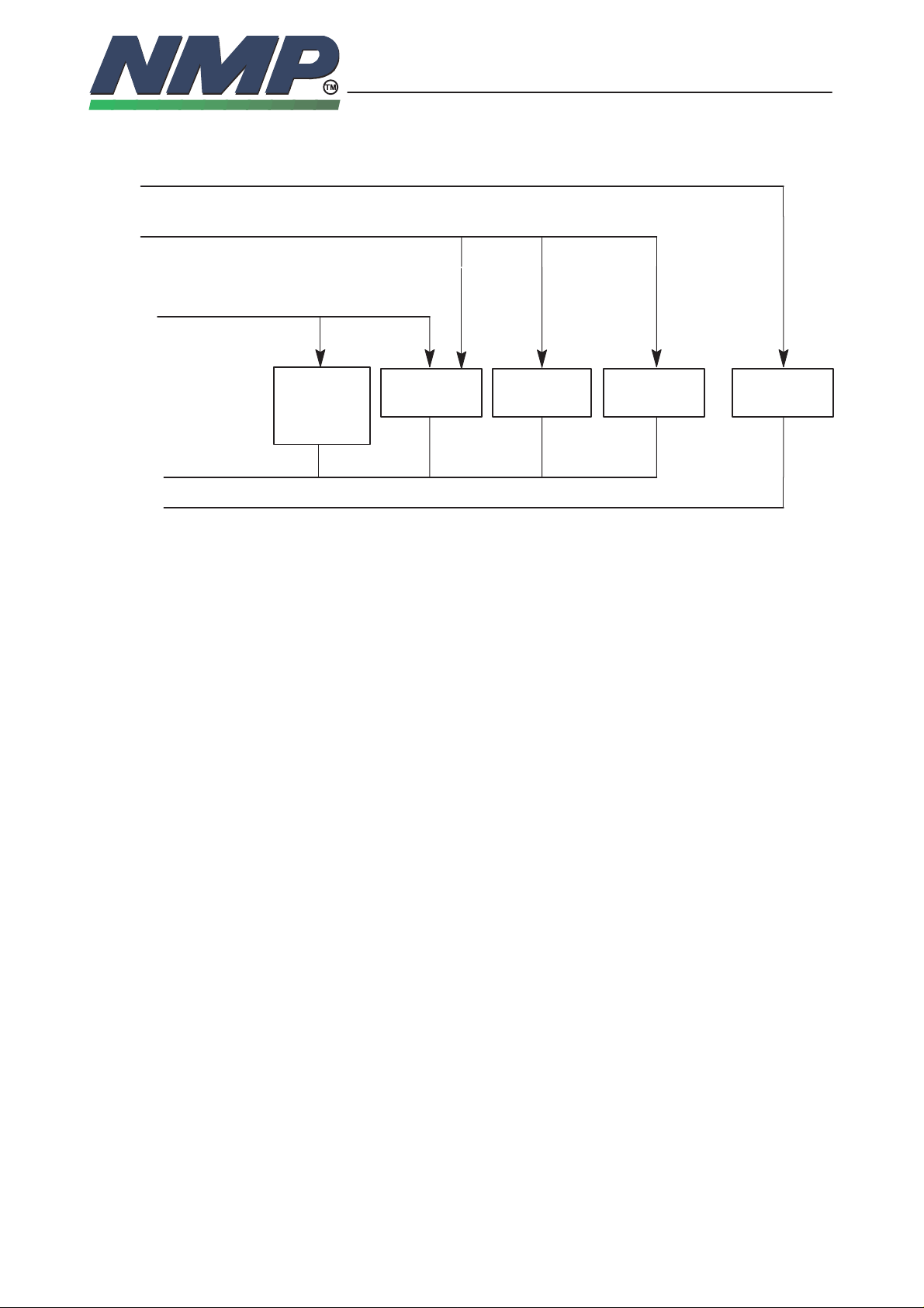
Power Distribution Diagram
VA
VL1
VBATT
KEY/
LCD
Lights
GND
AGND
9–9
Copyright Nokia Mobile Phones
LCDBUZZER
Keyboard
scan
Audio
Page 10

UIF MODULE GU1 VERSIONS
NHE–3 NHK–3
11/97 OJ
Technical Documentation
Copyright Nokia Mobile Phones
Parts List of GU1N
Code: 0200467 EDMS Issue: 6.0
ITEM CODE DESCRIPTION VALUE TYPE
R001 1430065 Chip resistor 10 k 5 % 0.063 W 0603
R002 1430087 Chip resistor 100 k 5 % 0.063 W 0603
R003 1430065 Chip resistor 10 k 5 % 0.063 W 0603
R004 1430087 Chip resistor 100 k 5 % 0.063 W 0603
R005 1430065 Chip resistor 10 k 5 % 0.063 W 0603
R006 1430087 Chip resistor 100 k 5 % 0.063 W 0603
R007 1430065 Chip resistor 10 k 5 % 0.063 W 0603
R008 1430087 Chip resistor 100 k 5 % 0.063 W 0603
R009 1430065 Chip resistor 10 k 5 % 0.063 W 0603
R010 1430087 Chip resistor 100 k 5 % 0.063 W 0603
R011 1430051 Chip resistor 4.7 k 5 % 0.063 W 0603
R012 1430051 Chip resistor 4.7 k 5 % 0.063 W 0603
R013 1430087 Chip resistor 100 k 5 % 0.063 W 0603
R016 1430151 Chip resistor 10 5 % 0.063 W 0603
R017 1430151 Chip resistor 10 5 % 0.063 W 0603
R018 1430063 Chip resistor 12 k 5 % 0.063 W 0603
R019 1800619 NTC resistor 15 k 10 % 1206
R020 1430041 Chip resistor 1.8 k 5 % 0.063 W 0603
R021 1430087 Chip resistor 100 k 5 % 0.063 W 0603
R022 1430081 Chip resistor 56 k 5 % 0.063 W 0603
R023 1430163 Chip resistor 33 5 % 0.063 W 0603
R024 1430087 Chip resistor 100 k 5 % 0.063 W 0603
R025 1430073 Chip resistor 27 k 5 % 0.063 W 0603
R026 1430073 Chip resistor 27 k 5 % 0.063 W 0603
R027 1430073 Chip resistor 27 k 5 % 0.063 W 0603
R028 1430073 Chip resistor 27 k 5 % 0.063 W 0603
R029 1430073 Chip resistor 27 k 5 % 0.063 W 0603
R030 1430087 Chip resistor 100 k 5 % 0.063 W 0603
R031 1430087 Chip resistor 100 k 5 % 0.063 W 0603
R032 1430065 Chip resistor 10 k 5 % 0.063 W 0603
R033 1430075 Chip resistor 33 k 5 % 0.063 W 0603
R034 1430035 Chip resistor 1.0 k 5 % 0.063 W 0603
R035 1430035 Chip resistor 1.0 k 5 % 0.063 W 0603
R053 1430013 Chip resistor 330 5 % 0.063 W 0603
R055 1430045 Chip resistor 2.7 k 5 % 0.063 W 0603
R056 1430045 Chip resistor 2.7 k 5 % 0.063 W 0603
R057 1430087 Chip resistor 100 k 5 % 0.063 W 0603
R058 1430159 Chip resistor 22 5 % 0.063 W 0603
R060 1430163 Chip resistor 33 5 % 0.063 W 0603
R062 1430151 Chip resistor 10 5 % 0.063 W 0603
R064 1430151 Chip resistor 10 5 % 0.063 W 0603
R065 1430151 Chip resistor 10 5 % 0.063 W 0603
9–10
Page 11

UIF MODULE GU1 VERSIONS
NHE–3 NHK–3
11/97 OJ
Technical Documentation
Copyright Nokia Mobile Phones
R066 1430151 Chip resistor 10 5 % 0.063 W 0603
R067 1430087 Chip resistor 100 k 5 % 0.063 W 0603
C001 2310791 Ceramic cap. 33 n 20 % 50 V 0805
C002 2310424 Ceramic cap. 100 p 5 % 50 V 0805
C003 2310791 Ceramic cap. 33 n 20 % 50 V 0805
C004 2310791 Ceramic cap. 33 n 20 % 50 V 0805
C005 2604209 Tantalum cap. 1.0 u 20 % 16 V 3.2x1.6x1.6
C006 2320041 Ceramic cap. 18 p 5 % 50 V 0603
C007 2320041 Ceramic cap. 18 p 5 % 50 V 0603
C008 2320041 Ceramic cap. 18 p 5 % 50 V 0603
C009 2320041 Ceramic cap. 18 p 5 % 50 V 0603
C010 2307816 Ceramic cap. 47 n 20 % 25 V 0805
C011 2307816 Ceramic cap. 47 n 20 % 25 V 0805
C027 2320107 Ceramic cap. 10 n 5 % 50 V 0603
C030 2320041 Ceramic cap. 18 p 5 % 50 V 0603
C031 2320041 Ceramic cap. 18 p 5 % 50 V 0603
H001 4850052 IC, dotmx16+45ind+2x7sgm eurDSL17 EURO
V001 4210100 Transistor BC848W npn 30 V SOT323
V002 4110070 Diode BAS16W 75 V 0.25 A SOT323
V004 4210102 Transistor BC858W pnp 30 V 100 mA
200MWSOT323
V005 4210100 Transistor BC848W npn 30 V SOT323
V006 4110070 Diode BAS16W 75 V 0.25 A SOT323
V011 4110070 Diode BAS16W 75 V 0.25 A SOT323
V012 4200836 Transistor BCX19 npn 50 V 0.5 A SOT23
V014 4210100 Transistor BC848W npn 30 V SOT323
V015 4864388 Led Green 0603
V016 4864388 Led Green 0603
V017 4200836 Transistor BCX19 npn 50 V 0.5 A SOT23
V018 4864388 Led Green 0603
V019 4864388 Led Green 0603
V020 4864388 Led Green 0603
V021 4864388 Led Green 0603
V022 4864388 Led Green 0603
V023 4864388 Led Green 0603
V024 4864388 Led Green 0603
V025 4864388 Led Green 0603
V026 4864388 Led Green 0603
V027 4864388 Led Green 0603
V029 4864388 Led Green 0603
V030 4864388 Led Green 0603
V031 4864388 Led Green 0603
V032 4864388 Led Green 0603
V033 4200836 Transistor BCX19 npn 50 V 0.5 A SOT23
D001 4309921 IC, 6 x inverter 74HC04 SO14
D002 4309047 IC, LCD driver uPD7228 QFP80
X001 5469490 SM, conn f 40pol pitch0.8mm pcb/p PCB/PCB
X002 5449506 Pin header 1x02 1.25mm angle smd SMD
9–11
Page 12

UIF MODULE GU1 VERSIONS
NHE–3 NHK–3
11/97 OJ
Technical Documentation
Copyright Nokia Mobile Phones
X003 5449506 Pin header 1x02 1.25mm angle smd SMD
X004 5449506 Pin header 1x02 1.25mm angle smd SMD
5140018 Buzzer+conn 85db 2700hz 5v d9x5.5 d9x5.5
5140458 Mic+wire 61.5+–2db1khz/2k/3v d6x3 D6x3
5140580 Speaker+conn 95.5+– 2DB 32R D20X2d20x2
9460100 Mic boot b10538
9460129 Light quide 4C24297
9480078 Buzzer gasket 4D23092 NHK–1XA
9853991 PCB GU1 163.3X50.0X0.4MM D 2/PA
9853991 PC board GU1 163.3x50.0x0.4mm d
2/p2/PA
9–12
Page 13

UIF MODULE GU1 VERSIONS
NHE–3 NHK–3
11/97 OJ
Technical Documentation
Copyright Nokia Mobile Phones
Parts List of GU1T
Code: 0200468 EDMS Issue: 6.0
ITEM CODE DESCRIPTION VALUE TYPE
R001 1430065 Chip resistor 10 k 5 % 0.063 W 0603
R002 1430087 Chip resistor 100 k 5 % 0.063 W 0603
R003 1430065 Chip resistor 10 k 5 % 0.063 W 0603
R004 1430087 Chip resistor 100 k 5 % 0.063 W 0603
R005 1430065 Chip resistor 10 k 5 % 0.063 W 0603
R006 1430087 Chip resistor 100 k 5 % 0.063 W 0603
R007 1430065 Chip resistor 10 k 5 % 0.063 W 0603
R008 1430087 Chip resistor 100 k 5 % 0.063 W 0603
R009 1430065 Chip resistor 10 k 5 % 0.063 W 0603
R010 1430087 Chip resistor 100 k 5 % 0.063 W 0603
R011 1430051 Chip resistor 4.7 k 5 % 0.063 W 0603
R012 1430051 Chip resistor 4.7 k 5 % 0.063 W 0603
R013 1430087 Chip resistor 100 k 5 % 0.063 W 0603
R016 1430151 Chip resistor 10 5 % 0.063 W 0603
R017 1430151 Chip resistor 10 5 % 0.063 W 0603
R018 1430063 Chip resistor 12 k 5 % 0.063 W 0603
R019 1800619 NTC resistor 15 k 10 % 1206
R020 1430041 Chip resistor 1.8 k 5 % 0.063 W 0603
R021 1430087 Chip resistor 100 k 5 % 0.063 W 0603
R022 1430081 Chip resistor 56 k 5 % 0.063 W 0603
R023 1430163 Chip resistor 33 5 % 0.063 W 0603
R024 1430087 Chip resistor 100 k 5 % 0.063 W 0603
R025 1430073 Chip resistor 27 k 5 % 0.063 W 0603
R026 1430073 Chip resistor 27 k 5 % 0.063 W 0603
R027 1430073 Chip resistor 27 k 5 % 0.063 W 0603
R028 1430073 Chip resistor 27 k 5 % 0.063 W 0603
R029 1430073 Chip resistor 27 k 5 % 0.063 W 0603
R030 1430087 Chip resistor 100 k 5 % 0.063 W 0603
R031 1430087 Chip resistor 100 k 5 % 0.063 W 0603
R032 1430065 Chip resistor 10 k 5 % 0.063 W 0603
R033 1430075 Chip resistor 33 k 5 % 0.063 W 0603
R034 1430035 Chip resistor 1.0 k 5 % 0.063 W 0603
R035 1430035 Chip resistor 1.0 k 5 % 0.063 W 0603
R053 1430013 Chip resistor 330 5 % 0.063 W 0603
R055 1430045 Chip resistor 2.7 k 5 % 0.063 W 0603
R056 1430045 Chip resistor 2.7 k 5 % 0.063 W 0603
R057 1430087 Chip resistor 100 k 5 % 0.063 W 0603
R058 1430159 Chip resistor 22 5 % 0.063 W 0603
R060 1430163 Chip resistor 33 5 % 0.063 W 0603
R061 1430151 Chip resistor 10 5 % 0.063 W 0603
R063 1430151 Chip resistor 10 5 % 0.063 W 0603
R065 1430151 Chip resistor 10 5 % 0.063 W 0603
9–13
Page 14

UIF MODULE GU1 VERSIONS
NHE–3 NHK–3
11/97 OJ
Technical Documentation
Copyright Nokia Mobile Phones
R066 1430151 Chip resistor 10 5 % 0.063 W 0603
R067 1430087 Chip resistor 100 k 5 % 0.063 W 0603
C001 2310791 Ceramic cap. 33 n 20 % 50 V 0805
C002 2310424 Ceramic cap. 100 p 5 % 50 V 0805
C003 2310791 Ceramic cap. 33 n 20 % 50 V 0805
C004 2310791 Ceramic cap. 33 n 20 % 50 V 0805
C005 2604209 Tantalum cap. 1.0 u 20 % 16 V 3.2x1.6x1.6
C006 2320041 Ceramic cap. 18 p 5 % 50 V 0603
C007 2320041 Ceramic cap. 18 p 5 % 50 V 0603
C008 2320041 Ceramic cap. 18 p 5 % 50 V 0603
C009 2320041 Ceramic cap. 18 p 5 % 50 V 0603
C010 2307816 Ceramic cap. 47 n 20 % 25 V 0805
C011 2307816 Ceramic cap. 47 n 20 % 25 V 0805
C027 2320107 Ceramic cap. 10 n 5 % 50 V 0603
C030 2320041 Ceramic cap. 18 p 5 % 50 V 0603
C031 2320041 Ceramic cap. 18 p 5 % 50 V 0603
H001 4850052 IC, dotmx16+45ind+2x7sgm eurDSL17 EURO
V001 4210100 Transistor BC848W npn 30 V SOT323
V002 4110070 Diode BAS16W 75 V 0.25 A SOT323
V004 4210102 Transistor BC858W pnp 30 V 100 mA
200MWSOT323
V005 4210100 Transistor BC848W npn 30 V SOT323
V006 4110070 Diode BAS16W 75 V 0.25 A SOT323
V011 4110070 Diode BAS16W 75 V 0.25 A SOT323
V012 4200836 Transistor BCX19 npn 50 V 0.5 A SOT23
V014 4210100 Transistor BC848W npn 30 V SOT323
V015 4864388 Led Green 0603
V016 4864388 Led Green 0603
V017 4200836 Transistor BCX19 npn 50 V 0.5 A SOT23
V018 4864388 Led Green 0603
V019 4864388 Led Green 0603
V020 4864388 Led Green 0603
V021 4864388 Led Green 0603
V022 4864388 Led Green 0603
V023 4864388 Led Green 0603
V024 4864388 Led Green 0603
V025 4864388 Led Green 0603
V026 4864388 Led Green 0603
V027 4864388 Led Green 0603
V029 4864388 Led Green 0603
V030 4864388 Led Green 0603
V031 4864388 Led Green 0603
V032 4864388 Led Green 0603
V033 4200836 Transistor BCX19 npn 50 V 0.5 A SOT23
D001 4309921 IC, 6 x inverter 74HC04 SO14
D002 4309047 IC, LCD driver uPD7228 QFP80
X001 5469490 SM, conn f 40pol pitch0.8mm pcb/p PCB/PCB
X002 5449506 Pin header 1x02 1.25mm angle smd SMD
9–14
Page 15

UIF MODULE GU1 VERSIONS
NHE–3 NHK–3
11/97 OJ
Technical Documentation
Copyright Nokia Mobile Phones
X003 5449506 Pin header 1x02 1.25mm angle smd SMD
X004 5449506 Pin header 1x02 1.25mm angle smd SMD
5140018 Buzzer+conn 85db 2700hz 5v d9x5.5 d9x5.5
5140458 Mic+wire 61.5+–2db1khz/2k/3v d6x3 D6x3
5140580 Speaker+conn 95.5+– 2DB 32R D20X2d20x2
9460100 Mic boot b10538
9460129 Light quide 4C24297
9480078 Buzzer gasket 4D23092 NHK–1XA
9853991 PCB GU1 163.3X50.0X0.4MM D 2/PA
9853991 PC board GU1 163.3x50.0x0.4mm d
2/p2/PA
9–15
Page 16

UIF MODULE GU1 VERSIONS
NHE–3 NHK–3
11/97 OJ
Technical Documentation
Copyright Nokia Mobile Phones
Parts List of GU1MN
Code: 0200564 EDMS Issue: 2.2
ITEM CODE DESCRIPTION VALUE TYPE
R001 1430065 Chip resistor 10 k 5 % 0.063 W 0603
R002 1430087 Chip resistor 100 k 5 % 0.063 W 0603
R003 1430065 Chip resistor 10 k 5 % 0.063 W 0603
R004 1430087 Chip resistor 100 k 5 % 0.063 W 0603
R005 1430065 Chip resistor 10 k 5 % 0.063 W 0603
R006 1430087 Chip resistor 100 k 5 % 0.063 W 0603
R007 1430065 Chip resistor 10 k 5 % 0.063 W 0603
R008 1430087 Chip resistor 100 k 5 % 0.063 W 0603
R009 1430065 Chip resistor 10 k 5 % 0.063 W 0603
R010 1430087 Chip resistor 100 k 5 % 0.063 W 0603
R011 1430051 Chip resistor 4.7 k 5 % 0.063 W 0603
R012 1430051 Chip resistor 4.7 k 5 % 0.063 W 0603
R013 1430081 Chip resistor 56 k 5 % 0.063 W 0603
R016 1430151 Chip resistor 10 5 % 0.063 W 0603
R017 1430151 Chip resistor 10 5 % 0.063 W 0603
R018 1430063 Chip resistor 12 k 5 % 0.063 W 0603
R019 1800619 NTC resistor 15 k 10 % 1206
R020 1430041 Chip resistor 1.8 k 5 % 0.063 W 0603
R021 1430087 Chip resistor 100 k 5 % 0.063 W 0603
R022 1430081 Chip resistor 56 k 5 % 0.063 W 0603
R023 1430163 Chip resistor 33 5 % 0.063 W 0603
R024 1430087 Chip resistor 100 k 5 % 0.063 W 0603
R025 1430073 Chip resistor 27 k 5 % 0.063 W 0603
R026 1430073 Chip resistor 27 k 5 % 0.063 W 0603
R027 1430073 Chip resistor 27 k 5 % 0.063 W 0603
R028 1430073 Chip resistor 27 k 5 % 0.063 W 0603
R029 1430073 Chip resistor 27 k 5 % 0.063 W 0603
R030 1430087 Chip resistor 100 k 5 % 0.063 W 0603
R031 1430087 Chip resistor 100 k 5 % 0.063 W 0603
R032 1430065 Chip resistor 10 k 5 % 0.063 W 0603
R033 1430075 Chip resistor 33 k 5 % 0.063 W 0603
R034 1430035 Chip resistor 1.0 k 5 % 0.063 W 0603
R035 1430035 Chip resistor 1.0 k 5 % 0.063 W 0603
R053 1430013 Chip resistor 330 5 % 0.063 W 0603
R055 1430045 Chip resistor 2.7 k 5 % 0.063 W 0603
R056 1430045 Chip resistor 2.7 k 5 % 0.063 W 0603
R057 1430087 Chip resistor 100 k 5 % 0.063 W 0603
R058 1430159 Chip resistor 22 5 % 0.063 W 0603
R060 1430163 Chip resistor 33 5 % 0.063 W 0603
R062 1430151 Chip resistor 10 5 % 0.063 W 0603
R064 1430151 Chip resistor 10 5 % 0.063 W 0603
R065 1430151 Chip resistor 10 5 % 0.063 W 0603
9–16
Page 17

UIF MODULE GU1 VERSIONS
NHE–3 NHK–3
11/97 OJ
Technical Documentation
Copyright Nokia Mobile Phones
R066 1430151 Chip resistor 10 5 % 0.063 W 0603
R067 1430087 Chip resistor 100 k 5 % 0.063 W 0603
R068 1430087 Chip resistor 100 k 5 % 0.063 W 0603
C001 2310791 Ceramic cap. 33 n 20 % 50 V 0805
C002 2310424 Ceramic cap. 100 p 5 % 50 V 0805
C003 2310791 Ceramic cap. 33 n 20 % 50 V 0805
C004 2310791 Ceramic cap. 33 n 20 % 50 V 0805
C005 2604209 Tantalum cap. 1.0 u 20 % 16 V 3.2x1.6x1.6
C006 2320041 Ceramic cap. 18 p 5 % 50 V 0603
C007 2320041 Ceramic cap. 18 p 5 % 50 V 0603
C008 2320041 Ceramic cap. 18 p 5 % 50 V 0603
C009 2320041 Ceramic cap. 18 p 5 % 50 V 0603
C010 2307816 Ceramic cap. 47 n 20 % 25 V 0805
C011 2307816 Ceramic cap. 47 n 20 % 25 V 0805
C027 2320107 Ceramic cap. 10 n 5 % 50 V 0603
C030 2320041 Ceramic cap. 18 p 5 % 50 V 0603
C031 2320041 Ceramic cap. 18 p 5 % 50 V 0603
H001 4850052 IC, dotmx16+45ind+2x7sgm eurDSL17 EURO
V001 4210100 Transistor BC848W npn 30 V SOT323
V002 4110070 Diode BAS16W 75 V 0.25 A SOT323
V004 4210102 Transistor BC858W pnp 30 V 100 mA
200MWSOT323
V005 4210100 Transistor BC848W npn 30 V SOT323
V006 4110070 Diode BAS16W 75 V 0.25 A SOT323
V011 4110070 Diode BAS16W 75 V 0.25 A SOT323
V012 4200836 Transistor BCX19 npn 50 V 0.5 A SOT23
V014 4210100 Transistor BC848W npn 30 V SOT323
V015 4864388 Led Green 0603
V016 4864388 Led Green 0603
V017 4200836 Transistor BCX19 npn 50 V 0.5 A SOT23
V018 4864388 Led Green 0603
V019 4864388 Led Green 0603
V020 4864388 Led Green 0603
V021 4864388 Led Green 0603
V022 4864388 Led Green 0603
V023 4864388 Led Green 0603
V024 4864388 Led Green 0603
V025 4864388 Led Green 0603
V026 4864388 Led Green 0603
V027 4864388 Led Green 0603
V029 4864388 Led Green 0603
V030 4864388 Led Green 0603
V031 4864388 Led Green 0603
V032 4864388 Led Green 0603
V033 4200836 Transistor BCX19 npn 50 V 0.5 A SOT23
D001 4309921 IC, 6 x inverter 74HC04 SO14
D002 4309047 IC, LCD driver uPD7228 QFP80
X001 5469288 SM, conn 2x15 f p0.8 pcb/pcb 2.8 2.8MM
9–17
Page 18

UIF MODULE GU1 VERSIONS
NHE–3 NHK–3
11/97 OJ
Technical Documentation
Copyright Nokia Mobile Phones
X002 5449506 Pin header 1x02 1.25mm angle smd SMD
X003 5449506 Pin header 1x02 1.25mm angle smd SMD
X004 5449506 Pin header 1x02 1.25mm angle smd SMD
5140018 Buzzer+conn 85db 2700hz 5v d9x5.5 d9x5.5
5140458 Mic+wire 61.5+–2db1khz/2k/3v d6x3 D6x3
5140580 Speaker+conn 95.5+– 2DB 32R D20X2d20x2
9460100 Mic boot b10538
9460129 Light quide 4C24297
9480078 Buzzer gasket 4D23092 NHK–1XA
9854033 PCB GU1M 50.0X163.3X0.4 D 2/PA
9854033 PC board GU1M 50.0x163.3x0.4 d 2/pa
9–18
Page 19

UIF MODULE GU1 VERSIONS
NHE–3 NHK–3
11/97 OJ
Technical Documentation
Copyright Nokia Mobile Phones
Parts List of GU1MT
Code: 0200565 EDMS Issue: 2.2
ITEM CODE DESCRIPTION VALUE TYPE
R001 1430065 Chip resistor 10 k 5 % 0.063 W 0603
R002 1430087 Chip resistor 100 k 5 % 0.063 W 0603
R003 1430065 Chip resistor 10 k 5 % 0.063 W 0603
R004 1430087 Chip resistor 100 k 5 % 0.063 W 0603
R005 1430065 Chip resistor 10 k 5 % 0.063 W 0603
R006 1430087 Chip resistor 100 k 5 % 0.063 W 0603
R007 1430065 Chip resistor 10 k 5 % 0.063 W 0603
R008 1430087 Chip resistor 100 k 5 % 0.063 W 0603
R009 1430065 Chip resistor 10 k 5 % 0.063 W 0603
R010 1430087 Chip resistor 100 k 5 % 0.063 W 0603
R011 1430051 Chip resistor 4.7 k 5 % 0.063 W 0603
R012 1430051 Chip resistor 4.7 k 5 % 0.063 W 0603
R013 1430081 Chip resistor 56 k 5 % 0.063 W 0603
R016 1430151 Chip resistor 10 5 % 0.063 W 0603
R017 1430151 Chip resistor 10 5 % 0.063 W 0603
R018 1430063 Chip resistor 12 k 5 % 0.063 W 0603
R019 1800619 NTC resistor 15 k 10 % 1206
R020 1430041 Chip resistor 1.8 k 5 % 0.063 W 0603
R021 1430087 Chip resistor 100 k 5 % 0.063 W 0603
R022 1430081 Chip resistor 56 k 5 % 0.063 W 0603
R023 1430163 Chip resistor 33 5 % 0.063 W 0603
R024 1430087 Chip resistor 100 k 5 % 0.063 W 0603
R025 1430073 Chip resistor 27 k 5 % 0.063 W 0603
R026 1430073 Chip resistor 27 k 5 % 0.063 W 0603
R027 1430073 Chip resistor 27 k 5 % 0.063 W 0603
R028 1430073 Chip resistor 27 k 5 % 0.063 W 0603
R029 1430073 Chip resistor 27 k 5 % 0.063 W 0603
R030 1430087 Chip resistor 100 k 5 % 0.063 W 0603
R031 1430087 Chip resistor 100 k 5 % 0.063 W 0603
R032 1430065 Chip resistor 10 k 5 % 0.063 W 0603
R033 1430075 Chip resistor 33 k 5 % 0.063 W 0603
R034 1430035 Chip resistor 1.0 k 5 % 0.063 W 0603
R035 1430035 Chip resistor 1.0 k 5 % 0.063 W 0603
R053 1430013 Chip resistor 330 5 % 0.063 W 0603
R055 1430045 Chip resistor 2.7 k 5 % 0.063 W 0603
R056 1430045 Chip resistor 2.7 k 5 % 0.063 W 0603
R057 1430087 Chip resistor 100 k 5 % 0.063 W 0603
R058 1430159 Chip resistor 22 5 % 0.063 W 0603
R060 1430163 Chip resistor 33 5 % 0.063 W 0603
R061 1430151 Chip resistor 10 5 % 0.063 W 0603
R063 1430151 Chip resistor 10 5 % 0.063 W 0603
R065 1430151 Chip resistor 10 5 % 0.063 W 0603
9–19
Page 20

UIF MODULE GU1 VERSIONS
NHE–3 NHK–3
11/97 OJ
Technical Documentation
Copyright Nokia Mobile Phones
R066 1430151 Chip resistor 10 5 % 0.063 W 0603
R067 1430087 Chip resistor 100 k 5 % 0.063 W 0603
R068 1430087 Chip resistor 100 k 5 % 0.063 W 0603
C001 2310791 Ceramic cap. 33 n 20 % 50 V 0805
C002 2310424 Ceramic cap. 100 p 5 % 50 V 0805
C003 2310791 Ceramic cap. 33 n 20 % 50 V 0805
C004 2310791 Ceramic cap. 33 n 20 % 50 V 0805
C005 2604209 Tantalum cap. 1.0 u 20 % 16 V 3.2x1.6x1.6
C006 2320041 Ceramic cap. 18 p 5 % 50 V 0603
C007 2320041 Ceramic cap. 18 p 5 % 50 V 0603
C008 2320041 Ceramic cap. 18 p 5 % 50 V 0603
C009 2320041 Ceramic cap. 18 p 5 % 50 V 0603
C010 2307816 Ceramic cap. 47 n 20 % 25 V 0805
C011 2307816 Ceramic cap. 47 n 20 % 25 V 0805
C027 2320107 Ceramic cap. 10 n 5 % 50 V 0603
C030 2320041 Ceramic cap. 18 p 5 % 50 V 0603
C031 2320041 Ceramic cap. 18 p 5 % 50 V 0603
H001 4850052 IC, dotmx16+45ind+2x7sgm eurDSL17 EURO
V001 4210100 Transistor BC848W npn 30 V SOT323
V002 4110070 Diode BAS16W 75 V 0.25 A SOT323
V004 4210102 Transistor BC858W pnp 30 V 100 mA
200MWSOT323
V005 4210100 Transistor BC848W npn 30 V SOT323
V006 4110070 Diode BAS16W 75 V 0.25 A SOT323
V011 4110070 Diode BAS16W 75 V 0.25 A SOT323
V012 4200836 Transistor BCX19 npn 50 V 0.5 A SOT23
V014 4210100 Transistor BC848W npn 30 V SOT323
V015 4864388 Led Green 0603
V016 4864388 Led Green 0603
V017 4200836 Transistor BCX19 npn 50 V 0.5 A SOT23
V018 4864388 Led Green 0603
V019 4864388 Led Green 0603
V020 4864388 Led Green 0603
V021 4864388 Led Green 0603
V022 4864388 Led Green 0603
V023 4864388 Led Green 0603
V024 4864388 Led Green 0603
V025 4864388 Led Green 0603
V026 4864388 Led Green 0603
V027 4864388 Led Green 0603
V029 4864388 Led Green 0603
V030 4864388 Led Green 0603
V031 4864388 Led Green 0603
V032 4864388 Led Green 0603
V033 4200836 Transistor BCX19 npn 50 V 0.5 A SOT23
D001 4309921 IC, 6 x inverter 74HC04 SO14
D002 4309047 IC, LCD driver uPD7228 QFP80
X001 5469288 SM, conn 2x15 f p0.8 pcb/pcb 2.8 2.8MM
9–20
Page 21

UIF MODULE GU1 VERSIONS
NHE–3 NHK–3
11/97 OJ
Technical Documentation
Copyright Nokia Mobile Phones
X002 5449506 Pin header 1x02 1.25mm angle smd SMD
X003 5449506 Pin header 1x02 1.25mm angle smd SMD
X004 5449506 Pin header 1x02 1.25mm angle smd SMD
5140018 Buzzer+conn 85db 2700hz 5v d9x5.5 d9x5.5
5140458 Mic+wire 61.5+–2db1khz/2k/3v d6x3 D6x3
5140580 Speaker+conn 95.5+– 2DB 32R D20X2d20x2
9460100 Mic boot b10538
9460129 Light quide 4C24297
9480078 Buzzer gasket 4D23092 NHK–1XA
9854033 PCB GU1M 50.0X163.3X0.4 D 2/PA
9854033 PC board GU1M 50.0x163.3x0.4 d 2/pa
9–21
 Loading...