

DATA SHEET
NPN SILICON RF TWIN T RANSISTOR
PA831TC
µµµµ
NPN SILICON EPITAXIAL TRANSISTOR (WITH 2 DIFFERENT ELEMENTS)
IN A FLAT-LEAD 6-PIN THIN-TYPE ULTRA SUPER MINIMOLD PACKAGE
DESCRIPTION
The µPA831TC has built-in two different transistors (Q1 and Q2) for low noise amplification in the VHF band to
UHF band.
FEATURES
• Low noise
Q1 : NF = 1.2 dB TYP., Q2 : NF = 1.4 dB TYP.
CE
@f = 1 GHz, V
• High gain
21e
Q1 : |S
@f = 1 GHz, VCE = 3 V, IC = 7 mA
• Flat-lead 6-pin thin-type ultra super minimold package
• 2 different built-in transistors (2SC5006, 2SC5007)
= 3 V, IC = 7 mA
2
= 9.0 dB TYP., Q2 : |S
|
2
21e
= 12.0 dB TYP.
|
BUILT-IN TRANSISTORS
Q1 Q2
3-pin ultra super minimold part No. 2SC5006 2SC5007
ORDERING INFORMATION
Part Number Package Quantity Supplying Form
µ
PA831TC Loose products
µ
PA831TC-T1
Remark
Flat-lead 6-pin
thin-type ultra
super minimold
To order evaluation samples, please contact your local NEC sales office. (Part number for sample order:
PA831TC.)
µ
(50 pcs)
Taping products
(3 kp/reel)
Caution Electro-static sensitive devices
8 mm wide embossed tape.
Pin 6 (Q1 Base), pin 5 (Q2 Emitter), pin 4 (Q2 Base) face to perforation
side of the tape.
The information in this document is subject to change without notice. Before using this document, please
confirm that this is the latest version.
Not all devices/types available in every country. Please check with local NEC representative for
availability and additional information.
Document No. P14554EJ1V0DS00 (1st edition)
Date Published November 1999 N CP(K)
Printed in Japan
1999©
µµµµ
PA831TC
ABSOLUTE MAXIMUM RATINGS (TA = +25
Parameter Symbol
Collector to Base Voltage V
Collector to Emitter Voltage V
Emitter to Base Voltage V
Collector Current I
Total Power Dissipat i on
Junction Temperature T
Storage Temperature T
2
Mounted on 1.08 cm
Note
× 1.0 mm glass epoxy substrate.
CBO
CEO
EBO
C
Note
T
P
j
stg
ELECTRICAL CHARACTERISTICS (TA = +25
(1) Q1
C)
°°°°
Ratings
Q1 Q2
20 20 V
12 10 V
31.5V
100 65 mA
200 in 1 element 200 in 1 element mW
230 in 2 elements
150 150
65 to +150
−
C)
°°°°
Unit
C
°
C
°
Parameter Symbol Conditions MIN. TYP. MAX. Unit
Collector Cutoff Current I
Emitter Cutoff Current I
DC Current Gain h
Gain Bandwidth Product f
Feedback Capacitance C
Insertion Power Gain
CBO
EBO
FE
T
21e
S
|
VCB = 10 V, IE = 0
VEB = 1 V, IC = 0
VCE = 3 V, IC = 7 mA
Note 1
VCE = 3 V, IC = 7 mA, f = 1 GHz 3.0 4.5
VCB = 3 V, IE = 0, f = 1 MHz
re
2
VCE = 3 V, IC = 7 mA, f = 1 GHz 7.0 9.0
|
Noise Figure NF VCE = 3 V, IC = 7 mA, f = 1 GHz
Notes 1.
Pulse Measurement: PW ≤ 350
Collector to base capacitance when measured with capacitance meter (automatic balanced bridge
2.
s, Duty Cycle ≤ 2%
µ
method), with emitter connected to guard pin of capacitance meter.
Note 2
−−
−−
70
−
−
−
0.7 1.5 pF
1.2 2.5 dB
1.0
1.0
140
−
−
A
µ
A
µ
GHz
dB
2
Data Sheet P14554EJ1V0DS00

(2) Q2
µµµµ
PA831TC
Parameter Symbol Conditions MIN. TYP. MAX. Unit
Collector Cutoff Current I
Emitter Cutoff Current I
DC Current Gain h
Gain Bandwidth Product f
Feedback Capacitance C
Insertion Power Gain
CBO
EBO
FE
T
21e
S
|
VCB = 10 V, IE = 0
VEB = 1 V, IC = 0
VCE = 3 V, IC = 7 mA
Note 1
VCE = 3 V, IC = 7 mA, f = 1 GHz 4.5 7.0
VCB = 3 V, IE = 0, f = 1 MHz
re
2
VCE = 3 V, IC = 7 mA, f = 1 GHz 10.0 12.0
|
Noise Figure NF VCE = 3 V, IC = 7 mA, f = 1 GHz
Notes 1.
Pulse Measurement: PW ≤ 350
Collector to base capacitance when measured with capacitance meter (automatic balanced bridge
2.
s, Duty Cycle ≤ 2%
µ
method), with emitter connected to guard pin of capacitance meter.
hFE CLASSIFICATION
Rank FB
Marking 24
hFE Value of Q1 70 to 140
hFE Value of Q2 70 to 150
Note 2
−−
−−
70
−
−−
−
1.4 2.7 dB
0.8
0.8
150
−
GHz
0.9 pF
−
µ
µ
dB
A
A
Data Sheet P14554EJ1V0DS00
3
µµµµ
PA831TC
TYPICAL CHARACTERISTICS (TA = +25
Q1 Q2
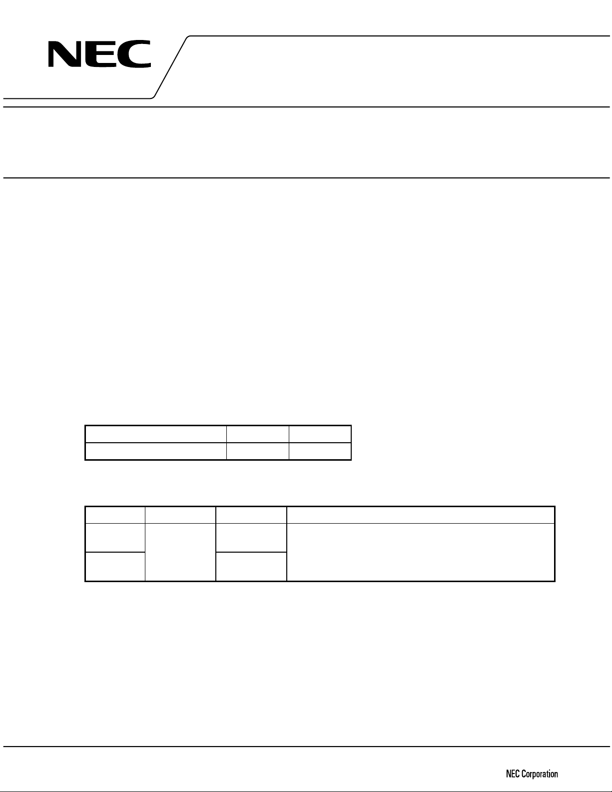
TOTAL POWER DISSIPATION vs.
AMBIENT TEMPERATURE
2 Elements in total Free Air Free Air
230
200
(mW)
T
Per Element
100
Total Power Dissipation P
0
0 50 100 150
Ambient Temperature TA (°C)
COLLECTOR CURRENT vs.
BASE TO EMITTER VOLTAGE
20
VCE = 3 V
C)
°°°°
TOTAL POWER DISSIPATION vs.
AMBIENT TEMPERATURE
2 Elements in total
230
200
(mW)
T
Per Element
100
Total Power Dissipation P
0
0 50 100 150
Ambient Temperature TA (°C)
COLLECTOR CURRENT vs.
BASE TO EMITTER VOLTAGE
20
VCE = 3 V
(mA)
C
10
Collector Current I
0
0
Base to Emitter Voltage VBE (V)
COLLECTOR CURRENT vs.
COLLECTOR TO EMITTER VOLTAGE
20
18
16
14
(mA)
C
12
10
8
6
Collector Current I
4
2
0
123456
0
Collector to Emitter Voltage VCE (V)
0.5 1.0
I
B
= 160 A
µ
IB = 140 A
µ
IB = 120 A
µ
IB = 100 A
µ
IB = 80 A
µ
IB = 60 A
µ
IB = 40 A
µ
IB = 20 A
µ
(mA)
C
10
Collector Current I
0
0
Base to Emitter Voltage VBE (V)
COLLECTOR CURRENT vs.
COLLECTOR TO EMITTER VOLTAGE
25
20
(mA)
C
15
10
Collector Current I
5
0
0
123456
Collector to Emitter Voltage VCE (V)
0.5 1.0
IB = 160 A
µ
IB = 140 A
µ
IB = 120 A
µ
IB = 100 A
µ
IB = 80 A
µ
IB = 60 A
µ
IB = 40 A
µ
IB = 20 A
µ
4
Data Sheet P14554EJ1V0DS00
µµµµ
PA831TC
1 000
100
DC Current Gain hFE
10
7.00
6.00
5.00
4.00
3.00
2.00
1.00
Gain Bandwidth Product fT (GHz)
0.00
0.1
VCE = 3 V
f = 1 GHz
1
Q1
DC CURRENT GAIN vs.
COLLECTOR CURRENT
VCE = 3 V
1 10 100
Collector Current IC (mA)
GAIN BANDWIDTH PRODUCT vs.
COLLECTOR CURRENT
10 100
Collector Current IC (mA)
1 000
100
DC Current Gain hFE
10
8.00
7.00
6.00
5.00
4.00
3.00
2.00
1.00
Gain Bandwidth Product fT (GHz)
0.00
0.1
VCE = 3 V
f = 1 GHz
1
Q2
DC CURRENT GAIN vs.
COLLECTOR CURRENT
VCE = 3 V
110
Collector Current IC (mA)
GAIN BANDWIDTH PRODUCT vs.
COLLECTOR CURRENT
10 100
Collector Current IC (mA)
INSERTION POWER GAIN vs.
COLLECTOR CURRENT
14.00
VCE = 3 V
f = 1 GHz
12.00
(dB)
2
10.00
8.00
6.00
4.00
Insertion Power Gain S21e
2.00
1 10 100
Collector Current IC (mA)
16.00
14.00
(dB)
2
12.00
10.00
8.00
6.00
4.00
Insertion Power Gain S21e
2.00
Data Sheet P14554EJ1V0DS00
INSERTION POWER GAIN vs.
COLLECTOR CURRENT
VCE = 3 V
f = 1 GHz
1 10 100
Collector Current IC (mA)
5

Q1 Q2
µµµµ
PA831TC
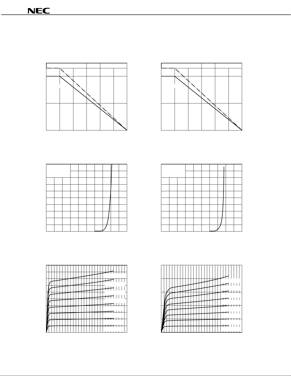
INSERTION POWER GAIN vs. FREQUENCY
25.0
(dB)
2
20.0
21e
15.0
10.0
5.0
Insertion Power Gain S
0.0
0.1
1.0 10.0
Frequency f (GHz)
NOISE FIGURE vs. COLLECTOR CURRENT
6.00
VCE = 3 V
f = 1 GHz
5.00
4.00
VCE = 3 V
C
= 7 mA
I
INSERTION POWER GAIN vs. FREQUENCY
25.0
(dB)
2
20.0
21e
15.0
10.0
5.0
Insertion Power Gain S
0.0
0.1
1.0 10.0
Frequency f (GHz)
NOISE FIGURE vs. COLLECTOR CURRENT
6.00
VCE = 3 V
f = 1 GHz
5.00
4.00
VCE = 3 V
C
= 7 mA
I
3.00
2.00
Noise Figure NF (dB)
1.00
0.00
1 10 100
Collector Current IC (mA)
FEEDBACK CAPACITANCE vs.
COLLECTOR TO BASE VOLTAGE
0.900
0.800
(pF)
0.700
re
0.600
0.500
0.400
0.300
0.200
Feedback Capacitance C
0.100
0.000
1 10 100
Collector to Base Voltage VCB (V)
f = 1 MHz
3.00
2.00
Noise Figure NF (dB)
1.00
0.00
1 10 100
Collector Current IC (mA)
FEEDBACK CAPACITANCE vs.
COLLECTOR TO BASE VOLTAGE
0.500
0.450
(pF)
0.400
re
0.350
0.300
0.250
0.200
0.150
0.100
Feedback Capacitance C
0.050
0.000
1 10 100
Collector to Base Voltage VCB (V)
f = 1 MHz
6
Data Sheet P14554EJ1V0DS00

µµµµ
PA831TC
S-PARAMETERS Q1
VCE = 3 V, IC = 1 mA
FREQUENCY S
GHz MAG.ANG.MAG.ANG.MAG.ANG.MAG.ANG.
11
21
S
12
S
S
22
0.1 0.938
0.2 0.913
0.3 0.881
0.4 0.843
0.5 0.816
0.6 0.782
0.7 0.759
0.8 0.748
0.9 0.739 165.9 1.700 34.1 0.158
1.0 0.730 152.1 1.572 22.7 0.158
1.1 0.731 138.6 1.461 11.8 0.158
1.2 0.726 125.8 1.364 1.0 0.153
1.3 0.730 113.7 1.277
1.4 0.730 101.7 1.203
1.5 0.735 90.6 1.131
1.6 0.736 79.6 1.069
1.7 0.741 69.1 1.017
1.8 0.743 58.7 0.967
1.9 0.750 48.8 0.925
2.0 0.751 39.0 0.878
2.1 0.757 29.6 0.840
2.2 0.761 20.1 0.800
2.3 0.767 11.3 0.770
2.4 0.770 1.9556 0.734
2.5 0.771
2.6 0.777
2.7 0.784
2.8 0.787
2.9 0.791
3.0 0.797
29.5 3.703 157.3 0.052 50.2 0.981
−
56.4 3.348 137.5 0.082 51.5 0.946
−
81.6 3.052 119.6 0.110 36.2 0.902
−
104.6 2.745 102.4 0.130 20.9 0.844
−
125.7 2.497 86.6 0.141 8.9 0.792
−
145.2 2.241 72.3 0.154
−
162.8 2.023 58.5 0.156
−
178.8 1.852 46.3 0.161
−
9.2 0.151
−
19.4 0.141
−
29.3 0.139
−
38.9 0.132
−
48.2 0.128
−
57.6 0.123
−
66.6 0.118
−
75.7 0.117
−
84.2 0.111
−
93.1 0.111
−
101.1 0.111
−
109.5 0.112
6.6 0.704
−
15.2 0.677
−
23.9 0.646
−
32.0 0.621
−
40.2 0.600
−
48.2 0.575
−
−
117.2 0.119
−
125.3 0.126
−
132.6 0.132
−
140.4 0.140
−
147.9 0.147
−
154.7 0.159
−
2.8 0.756
−
14.1 0.715
−
23.1 0.698
−
32.0 0.672
−
40.8 0.655
−
49.5 0.637
−
57.1 0.624
−
63.5 0.616
−
70.4 0.608
−
75.7 0.600
−
81.0 0.594
−
85.1 0.590
−
89.6 0.582
−
92.7 0.580
−
96.3 0.580 177.3
−
99.5 0.571 168.0
−
100.5 0.573 158.1
−
101.6 0.567 148.8
−
102.9 0.569 138.7
−
104.3 0.564 128.6
−
107.2 0.564 118.7
−
108.9 0.566 108.4
−
113.5 0.567 98.2
−
116.1 0.563 87.8
−
121.2 0.573 77.3
−
VCE = 3 V, IC = 3 mA
FREQUENCY S
GHz MAG.ANG.MAG.ANG.MAG.ANG.MAG.ANG.
11
21
S
12
S
S
13.9
−
26.3
−
37.6
−
48.3
−
57.1
−
66.1
−
73.8
−
82.0
−
90.0
−
97.8
−
106.0
−
113.7
−
122.2
−
130.2
−
138.6
−
147.4
−
156.3
−
165.0
−
174.2
−
22
0.1 0.929
0.2 0.881
0.3 0.834
0.4 0.774
0.5 0.730
0.6 0.683
0.7 0.654
0.8 0.632
0.9 0.611 172.1 2.747 38.2 0.180
1.0 0.600 157.6 2.543 27.1 0.178
1.1 0.594 144.2 2.360 16.3 0.186
1.2 0.587 130.9 2.202 6.0 0.188
1.3 0.587 118.7 2.062
1.4 0.588 106.5 1.943
1.5 0.590 95.2 1.834
1.6 0.595 84.0 1.731
1.7 0.596 73.3 1.648
1.8 0.600 62.7 1.571
1.9 0.606 52.8 1.504
2.0 0.614 42.6 1.436
2.1 0.617 33.1 1.367
2.2 0.623 23.8 1.309
2.3 0.630 14.3 1.262
2.4 0.635 5.4 1.210
2.5 0.641
2.6 0.648
2.7 0.653
2.8 0.660
2.9 0.668
3.0 0.673
27.6 5.790 157.9 0.050 42.1 0.987
−
53.5 5.401 138.4 0.085 57.3 0.929
−
77.2 4.951 120.9 0.107 41.0 0.865
−
99.8 4.477 103.7 0.130 28.1 0.785
−
120.0 4.065 88.5 0.147 16.9 0.713
−
138.9 3.641 74.6 0.161 6.4 0.660
−
156.1 3.309 61.7 0.168
−
172.9 3.007 49.6 0.174
−
4.0 0.193
−
13.7 0.193
−
23.4 0.194
−
33.0 0.199
−
42.2 0.199
−
51.7 0.199
−
60.4 0.204
−
69.5 0.207
−
78.4 0.208
−
87.4 0.209
−
95.6 0.211
−
104.1 0.214
3.3 1.162
−
11.7 1.121
−
20.4 1.080
−
28.6 1.044
−
36.6 1.014
−
44.9 0.977
−
−
112.4 0.217
−
120.5 0.222
−
128.4 0.223
−
136.7 0.229
−
144.1 0.232
−
152.2 0.235
−
−
−
−
−
−
3.7 0.602
−
12.5 0.560
−
20.3 0.524
−
27.6 0.495
−
35.4 0.467
−
41.6 0.444
−
48.8 0.427
−
55.1 0.410
−
61.7 0.396
−
67.2 0.380
−
73.4 0.371
−
79.2 0.359
−
85.7 0.348 175.1
−
90.8 0.340 166.2
−
97.3 0.329 157.2
−
102.8 0.322 147.9
−
108.6 0.314 138.5
−
113.6 0.310 128.9
−
119.5 0.303 119.4
−
124.6 0.300 109.6
−
130.4 0.295 99.2
−
136.0 0.297 90.3
−
141.5 0.295 80.0
−
147.8 0.301 69.7
−
−
−
−
103.3
−
111.3
−
119.6
−
127.3
−
135.3
−
143.2
−
151.1
−
160.0
−
168.2
−
176.2
−
16.6
30.8
45.1
57.2
68.1
77.6
86.9
95.1
Data Sheet P14554EJ1V0DS00
7

VCE = 3 V, IC = 5 mA
FREQUENCY S
11
GHz MAG.ANG.MAG.ANG.MAG.ANG.MAG.ANG.
21
S
12
S
S
µµµµ
PA831TC
22
0.1 0.787
0.2 0.708
0.3 0.662
0.4 0.619
0.5 0.603
50.1 14.281 144.6 0.052 33.3 0.928
−
91.6 11.299 119.6 0.058 48.6 0.722
−
121.9 9.080 100.3 0.075 23.0 0.603
−
146.9 7.356 84.3 0.082 19.3 0.503
−
166.4 6.183 70.9 0.084 10.7 0.433
−
0.6 0.591 176.8 5.269 58.8 0.090 3.6 0.378
0.7 0.587 162.0 4.599 48.1 0.091
0.8 0.588 148.6 4.073 37.8 0.096
0.9 0.586 136.5 3.652 27.6 0.100
1.0 0.590 124.6 3.319 18.2 0.101
1.1 0.594 114.0 3.043 8.7 0.107
1.2 0.596 103.2 2.798
1.3 0.603 93.4 2.603
1.4 0.607 82.9 2.423
1.5 0.614 73.6 2.274
1.6 0.623 64.6 2.137
1.7 0.628 55.6 2.018
1.8 0.632 46.4 1.899
1.9 0.640 37.7 1.819
2.0 0.646 28.8 1.724
2.1 0.656 20.5 1.642
2.2 0.660 11.9 1.568
2.3 0.668 4.0 1.506
2.4 0.674
2.5 0.677
2.6 0.685
2.7 0.693
2.8 0.697
2.9 0.706
3.0 0.713
4.0 1.442
−
12.4 1.383
−
20.1 1.330
−
27.8 1.286
−
35.6 1.235
−
43.4 1.194
−
50.6 1.151
−
0.5 0.114
−
9.4 0.115
−
18.4 0.122
−
27.0 0.127
−
36.0 0.133
−
44.6 0.138
−
53.1 0.142
−
61.3 0.148
−
69.8 0.155
−
78.0 0.164
−
86.6 0.168
−
94.4 0.173
−
102.7 0.181
−
110.4 0.187
−
118.4 0.195
−
126.3 0.201
−
133.9 0.204
−
141.8 0.213
−
149.5 0.221
−
1.5 0.346
−
8.8 0.314
−
10.5 0.294
−
16.9 0.274
−
23.1 0.264
−
26.6 0.250
−
31.4 0.244
−
36.1 0.234
−
41.7 0.221
−
46.7 0.216
−
51.2 0.209
−
57.0 0.204 175.9
−
62.2 0.200 166.0
−
67.4 0.197 155.6
−
73.8 0.193 145.4
−
79.3 0.192 134.8
−
84.3 0.189 123.6
−
90.6 0.190 113.2
−
96.3 0.191 101.6
−
101.7 0.195 90.0
−
108.7 0.197 79.2
−
114.4 0.205 68.3
−
120.5 0.208 57.3
−
125.8 0.217 47.6
−
VCE = 3 V, IC = 7 mA
FREQUENCY S
11
GHz MAG.ANG.MAG.ANG.MAG.ANG.MAG.ANG.
21
S
12
S
S
29.0
−
48.1
−
63.3
−
73.0
−
81.0
−
88.5
−
96.1
−
103.0
−
110.4
−
116.9
−
125.0
−
132.5
−
140.7
−
148.4
−
157.7
−
166.3
−
175.6
−
22
0.1 0.738
0.2 0.630
0.3 0.596
0.4 0.574
0.5 0.564
60.7 18.140 139.9 0.035 26.0 0.865
−
104.2 13.504 113.5 0.060 38.6 0.653
−
134.1 10.414 95.1 0.067 29.9 0.509
−
158.5 8.249 79.9 0.073 19.5 0.414
−
176.7 6.877 67.4 0.072 14.3 0.348
−
0.6 0.554 168.2 5.807 56.0 0.078 10.2 0.303
0.7 0.553 154.2 5.036 45.7 0.083 5.7 0.270
0.8 0.559 142.0 4.441 35.9 0.089 1.8 0.244
0.9 0.558 130.1 3.988 26.3 0.096
1.0 0.562 119.3 3.609 17.0 0.100
1.1 0.569 108.6 3.300 7.7 0.107
1.2 0.574 98.8 3.039
1.3 0.580 89.5 2.819
1.4 0.583 79.8 2.622
1.5 0.594 70.9 2.463
1.6 0.598 61.7 2.307
1.7 0.605 53.1 2.180
1.8 0.611 44.2 2.053
1.9 0.619 35.8 1.965
2.0 0.625 27.0 1.862
2.1 0.634 18.7 1.778
2.2 0.642 10.7 1.695
2.3 0.652 2.7 1.626
2.4 0.652
2.5 0.662
2.6 0.669
2.7 0.677
2.8 0.682
2.9 0.688
3.0 0.696
5.636 1.557
−
13.2 1.496
−
21.1 1.440
−
28.8 1.387
−
36.1 1.337
−
44.2 1.294
−
51.1 1.242
−
1.1 0.113
−
9.8 0.119
−
18.5 0.127
−
27.1 0.133
−
35.7 0.138
−
44.1 0.148
−
52.8 0.154
−
60.8 0.160
−
69.2 0.168
−
77.2 0.173
−
85.5 0.182
−
93.4 0.186
−
101.5 0.196
−
109.3 0.200
−
117.0 0.209
−
124.7 0.214
−
132.2 0.221
−
140.2 0.228
−
147.7 0.234
−
5.0 0.228
−
10.4 0.212
−
14.5 0.200
−
19.7 0.188
−
25.8 0.177
−
29.0 0.172
−
35.1 0.164
−
40.2 0.157
−
46.3 0.154 172.2
−
52.4 0.148 162.6
−
59.2 0.145 151.6
−
64.7 0.143 140.3
−
71.1 0.142 128.1
−
76.6 0.141 116.6
−
82.8 0.144 104.7
−
88.7 0.146 92.0
−
95.0 0.149 80.2
−
101.6 0.155 70.2
−
107.6 0.164 58.7
−
114.5 0.169 47.8
−
121.1 0.177 36.9
−
127.0 0.186 27.6
−
−
−
−
−
−
−
102.0
−
109.8
−
117.6
−
124.3
−
132.7
−
140.5
−
149.6
−
157.7
−
168.1
−
177.4
−
34.7
55.3
69.4
79.9
87.9
95.0
8
Data Sheet P14554EJ1V0DS00

µµµµ
PA831TC
S-PARAMETERS Q2
VCE = 3 V, IC = 1 mA
FREQUENCY S
GHz MAG.ANG.MAG.ANG.MAG.ANG.MAG.ANG.
11
21
S
12
S
S
22
0.1 0.960
0.2 0.943
0.3 0.922
0.4 0.885
0.5 0.862
0.6 0.821
0.7 0.790
0.8 0.759
0.9 0.728
1.0 0.706
1.1 0.685
1.2 0.671 168.5 2.087 24.7 0.148
1.3 0.659 155.7 1.979 14.5 0.147
1.4 0.645 143.1 1.891 4.6 0.145
1.5 0.641 131.1 1.808
1.6 0.635 119.1 1.730
1.7 0.629 107.2 1.652
1.8 0.623 96.0 1.592
1.9 0.626 85.0 1.532
2.0 0.621 74.1 1.468
2.1 0.620 63.5 1.413
2.2 0.620 53.5 1.362
2.3 0.623 43.7 1.318
2.4 0.621 33.6 1.270
2.5 0.626 24.3 1.230
2.6 0.626 15.2 1.195
2.7 0.635 6.4 1.161
2.8 0.635
2.9 0.639
3.0 0.647
19.1 3.823 163.5 0.020 74.9 0.984
−
37.8 3.597 148.4 0.051 62.2 0.981
−
54.3 3.422 134.7 0.065 48.6 0.961
−
72.3 3.252 120.1 0.084 40.6 0.926
−
89.0 3.105 106.6 0.101 28.1 0.899
−
105.0 2.916 93.3 0.114 17.6 0.860
−
120.6 2.754 80.8 0.124 7.1 0.833
−
135.5 2.595 69.1 0.130
−
150.2 2.445 57.4 0.139
−
164.6 2.316 46.0 0.141
−
178.3 2.194 35.2 0.144
−
5.2 0.147
−
15.4 0.144
−
24.8 0.143
−
34.3 0.142
−
43.4 0.139
−
52.7 0.138
−
61.4 0.135
−
70.6 0.133
−
79.0 0.131
−
87.8 0.131
−
96.2 0.133
−
104.9 0.137
−
113.3 0.138
2.2 1.122
−
10.6 1.095
−
18.5 1.050
−
−
121.7 0.146
−
130.0 0.154
−
138.3 0.164
−
5.0 0.803
−
13.2 0.775
−
20.7 0.748
−
29.9 0.724
−
38.6 0.708
−
46.7 0.688
−
53.0 0.672
−
59.4 0.655
−
66.9 0.639
−
72.8 0.627
−
79.1 0.614
−
84.4 0.603
−
89.5 0.597
−
94.7 0.585
−
99.6 0.576
−
104.2 0.568 175.4
−
107.7 0.560 167.6
−
112.2 0.551 159.1
−
114.3 0.544 150.8
−
116.8 0.533 142.3
−
120.9 0.526 133.9
−
124.0 0.511 125.7
−
131.3 0.504 117.6
−
VCE = 3 V, IC = 3 mA
FREQUENCY S
GHz MAG.ANG.MAG.ANG.MAG.ANG.MAG.ANG.
11
21
S
12
S
S
9.7
−
20.2
−
30.3
−
39.8
−
48.5
−
56.8
−
65.2
−
73.5
−
81.0
−
88.4
−
95.7
−
102.9
−
110.4
−
117.7
−
124.7
−
132.1
−
139.3
−
146.6
−
154.2
−
161.5
−
168.4
−
176.4
−
22
0.1 0.897
0.2 0.844
0.3 0.784
0.4 0.723
0.5 0.670
0.6 0.616
0.7 0.580
0.8 0.547
0.9 0.528
1.0 0.510 171.3 4.051 35.6 0.104
1.1 0.496 158.6 3.749 25.6 0.107
1.2 0.483 145.7 3.501 16.2 0.112
1.3 0.480 133.8 3.273 6.9 0.114
1.4 0.477 122.6 3.086
1.5 0.475 111.1 2.907
1.6 0.474 100.0 2.752
1.7 0.477 89.8 2.617
1.8 0.477 79.4 2.477
1.9 0.481 69.6 2.381
2.0 0.484 59.9 2.271
2.1 0.489 50.1 2.176
2.2 0.493 41.2 2.084
2.3 0.499 32.1 2.011
2.4 0.506 23.4 1.933
2.5 0.508 14.9 1.862
2.6 0.517 6.4 1.801
2.7 0.526
2.8 0.535
2.9 0.543
3.0 0.556
26.0 9.698 157.7 0.025 23.3 0.992
−
49.9 8.841 139.5 0.047 65.0 0.918
−
72.1 8.028 122.8 0.055 47.4 0.858
−
92.8 7.209 106.8 0.072 32.5 0.791
−
111.3 6.534 92.7 0.079 25.9 0.724
−
128.8 5.822 79.6 0.088 14.8 0.669
−
144.9 5.287 67.8 0.093 5.7 0.628
−
160.4 4.812 56.6 0.095
−
175.1 4.391 45.7 0.102
−
2.2 0.116
−
11.1 0.122
−
20.2 0.124
−
28.8 0.130
−
37.4 0.132
−
45.7 0.136
−
54.4 0.141
−
62.8 0.142
−
71.4 0.150
−
79.4 0.155
−
87.7 0.162
−
95.8 0.167
−
104.1 0.175
1.2 1.742
−
9.4 1.688
−
17.1 1.629
−
25.0 1.572
−
−
111.9 0.179
−
119.8 0.186
−
127.5 0.192
−
135.3 0.197
−
−
−
−
−
−
−
2.3 0.585
−
5.5 0.551
−
14.3 0.528
−
20.1 0.501
−
25.1 0.482
−
31.7 0.463
−
36.0 0.452
−
41.3 0.436
−
47.3 0.421
−
53.2 0.410
−
57.9 0.402
−
63.7 0.384
−
68.1 0.379
−
75.1 0.365
−
78.8 0.354
−
84.0 0.343 176.0
−
90.6 0.337 168.9
−
95.4 0.323 161.0
−
101.4 0.313 153.4
−
106.8 0.306 145.3
−
113.6 0.299 137.0
−
119.9 0.290 129.0
−
126.4 0.286 120.7
−
−
−
−
−
101.4
−
107.5
−
114.4
−
120.8
−
127.5
−
134.4
−
140.9
−
147.9
−
155.0
−
161.4
−
168.6
−
175.9
−
15.1
27.5
39.8
50.3
59.4
67.3
74.8
81.7
88.2
94.4
Data Sheet P14554EJ1V0DS00
9

VCE = 3 V, IC = 5 mA
FREQUENCY S
11
GHz MAG.ANG.MAG.ANG.MAG.ANG.MAG.ANG.
21
S
12
S
S
µµµµ
PA831TC
22
0.1 0.853
0.2 0.761
0.3 0.693
0.4 0.619
0.5 0.568
0.6 0.522
0.7 0.489
0.8 0.467
0.9 0.451 173.6 5.105 41.2 0.091
1.0 0.438 160.1 4.661 31.5 0.092
1.1 0.428 147.5 4.292 22.1 0.099
1.2 0.423 135.7 3.989 12.9 0.106
1.3 0.425 124.5 3.720 4.1 0.110
1.4 0.422 113.3 3.477
1.5 0.425 102.7 3.265
1.6 0.430 92.3 3.101
1.7 0.434 82.7 2.925
1.8 0.436 72.8 2.782
1.9 0.443 63.4 2.656
2.0 0.444 54.1 2.533
2.1 0.453 45.0 2.422
2.2 0.457 35.9 2.319
2.3 0.464 27.9 2.233
2.4 0.470 19.6 2.148
2.5 0.478 11.2 2.066
2.6 0.487 3.1 1.989
2.7 0.492
2.8 0.502
2.9 0.513
3.0 0.528
30.1 13.631 154.4 0.030 42.5 0.975
−
58.0 12.026 133.7 0.042 60.6 0.870
−
82.4 10.531 115.9 0.052 41.9 0.781
−
105.0 9.123 99.6 0.062 32.6 0.700
−
124.2 7.999 85.6 0.072 23.5 0.623
−
141.3 7.036 73.1 0.075 16.0 0.571
−
157.8 6.236 61.8 0.079 7.6 0.526
−
172.5 5.612 51.3 0.088 4.3 0.490
−
4.3 1.925
−
11.8 1.858
−
19.5 1.800
−
26.9 1.742
−
4.6 0.116
−
13.4 0.119
−
22.2 0.125
−
30.4 0.132
−
39.1 0.136
−
46.9 0.141
−
55.3 0.147
−
63.6 0.150
−
72.0 0.157
−
79.6 0.163
−
87.8 0.171
−
95.7 0.179
−
103.8 0.187
−
111.5 0.195
−
119.2 0.199
−
127.1 0.207
−
134.5 0.212
−
2.7 0.464
−
7.0 0.439
−
14.7 0.419
−
18.6 0.401
−
25.5 0.390
−
29.7 0.372
−
34.5 0.359
−
41.4 0.346
−
45.4 0.337
−
51.6 0.326
−
56.3 0.314
−
62.7 0.307
−
69.0 0.292
−
74.2 0.284
−
80.1 0.269 177.4
−
86.5 0.263 170.3
−
92.6 0.251 162.8
−
98.4 0.240 154.5
−
104.8 0.233 147.6
−
111.3 0.224 138.8
−
117.7 0.216 131.2
−
125.0 0.212 122.8
−
VCE = 3 V, IC = 7 mA
FREQUENCY S
11
GHz MAG.ANG.MAG.ANG.MAG.ANG.MAG.ANG.
21
S
12
S
S
17.5
−
32.4
−
45.3
−
54.9
−
63.4
−
70.6
−
76.8
−
83.3
−
89.8
−
95.3
−
101.9
−
107.8
−
114.5
−
120.6
−
127.4
−
133.8
−
140.6
−
147.0
−
153.9
−
160.7
−
166.9
−
174.8
−
22
0.1 0.877
0.2 0.801
0.3 0.736
0.4 0.662
0.5 0.600
0.6 0.551
0.7 0.511
0.8 0.483
0.9 0.457
27.1 18.049 149.6 0.034 55.5 0.978
−
51.8 15.160 127.2 0.041 50.5 0.897
−
74.3 12.633 108.8 0.056 40.2 0.823
−
94.3 10.579 92.9 0.070 36.1 0.733
−
112.8 9.065 79.3 0.076 28.3 0.657
−
130.4 7.838 67.4 0.084 18.4 0.601
−
146.4 6.848 56.8 0.089 10.3 0.553
−
161.7 6.110 46.6 0.096 3.1 0.513
−
175.8 5.518 37.0 0.102
−
1.0 0.441 170.6 5.024 27.8 0.108
1.1 0.430 157.9 4.604 18.7 0.113
1.2 0.418 144.9 4.256 9.9 0.117
1.3 0.416 133.5 3.965 1.4 0.120
1.4 0.411 121.9 3.709
1.5 0.412 110.8 3.481
1.6 0.411 99.8 3.273
1.7 0.415 89.7 3.108
1.8 0.416 79.2 2.952
1.9 0.421 69.7 2.819
2.0 0.426 60.0 2.676
2.1 0.431 50.5 2.560
2.2 0.434 41.7 2.452
2.3 0.439 32.7 2.360
2.4 0.446 24.2 2.270
2.5 0.450 15.6 2.187
2.6 0.461 7.2 2.117
2.7 0.467 0.2 2.037
2.8 0.474
2.9 0.488
3.0 0.513
7.7 1.969
−
14.6 1.919
−
21.5 1.856
−
7.0 0.128
−
15.6 0.131
−
23.9 0.139
−
31.9 0.146
−
40.5 0.149
−
48.3 0.156
−
56.4 0.161
−
64.6 0.164
−
72.6 0.175
−
80.4 0.178
−
88.3 0.187
−
96.0 0.193
−
104.1 0.204
−
111.5 0.210
−
119.4 0.219
−
127.1 0.225
−
134.7 0.230
−
−
−
−
−
−
−
−
−
3.0 0.476
−
8.6 0.445
−
14.8 0.423
−
21.3 0.402
−
26.5 0.381
−
30.6 0.363
−
37.1 0.348
−
43.4 0.332
−
48.8 0.321
−
54.1 0.306
−
60.5 0.292
−
65.8 0.283
−
72.3 0.268
−
78.0 0.259
−
84.3 0.244 173.6
−
89.9 0.235 166.6
−
95.8 0.222 159.0
−
102.5 0.213 151.9
−
108.0 0.203 143.8
−
115.1 0.194 136.2
−
122.8 0.189 129.6
−
131.1 0.188 120.8
−
−
100.0
−
106.3
−
113.1
−
119.0
−
125.5
−
131.8
−
138.4
−
145.7
−
151.5
−
158.9
−
165.2
−
171.6
−
178.7
−
16.4
31.8
44.8
55.1
64.4
72.8
80.1
86.7
93.6
10
Data Sheet P14554EJ1V0DS00

µµµµ
PA831TC
VCE = 3 V, IC = 10 mA
FREQUENCY S
GHz MAG.ANG.MAG.ANG.MAG.ANG.MAG.ANG.
11
21
S
12
S
S
22
0.1 0.871
0.2 0.797
0.3 0.731
0.4 0.656
0.5 0.597
0.6 0.541
0.7 0.503
0.8 0.472
0.9 0.449
1.0 0.427 172.7 5.319 25.1 0.110
1.1 0.415 159.9 4.860 16.3 0.116
1.2 0.405 147.0 4.488 7.8 0.120
1.3 0.403 135.3 4.168
1.4 0.400 123.6 3.885
1.5 0.399 112.4 3.652
1.6 0.396 101.8 3.440
1.7 0.402 91.4 3.246
1.8 0.406 80.7 3.084
1.9 0.411 70.3 2.936
2.0 0.413 60.6 2.795
2.1 0.420 50.8 2.681
2.2 0.425 41.5 2.558
2.3 0.434 32.5 2.460
2.4 0.438 23.7 2.368
2.5 0.446 14.8 2.275
2.6 0.459 6.8 2.204
2.7 0.467
2.8 0.476
2.9 0.480
3.0 0.489
27.4 23.109 145.2 0.023 28.8 0.963
−
50.9 18.315 120.2 0.042 60.1 0.893
−
72.7 14.604 101.8 0.059 43.2 0.824
−
93.2 11.812 86.7 0.069 34.2 0.738
−
111.6 9.921 74.1 0.073 27.5 0.661
−
128.1 8.442 63.1 0.084 18.4 0.593
−
144.8 7.366 52.6 0.090 9.5 0.542
−
159.6 6.535 43.2 0.101 2.9 0.502
−
173.5 5.869 34.1 0.106
−
0.6 0.128
−
8.7 0.133
−
16.8 0.140
−
25.3 0.146
−
33.4 0.152
−
41.7 0.159
−
49.1 0.163
−
57.3 0.169
−
65.2 0.173
−
73.3 0.181
−
80.9 0.185
−
88.6 0.194
−
96.3 0.198
−
104.1 0.206
1.7 2.122
−
10.2 2.050
−
18.4 1.999
−
26.4 1.931
−
−
111.8 0.213
−
119.3 0.217
−
126.9 0.221
−
134.4 0.228
−
−
−
−
−
−
−
−
0.5 0.467
−
6.8 0.435
−
14.7 0.408
−
19.4 0.385
−
25.5 0.367
−
31.0 0.344
−
36.3 0.329
−
43.6 0.314
−
48.1 0.300
−
54.6 0.285
−
60.4 0.268
−
66.3 0.258
−
72.5 0.238
−
78.7 0.232 177.6
−
84.5 0.216 169.6
−
91.0 0.208 162.4
−
97.5 0.192 154.5
−
102.5 0.180 146.1
−
109.1 0.170 138.9
−
115.4 0.162 129.4
−
121.6 0.147 120.9
−
128.2 0.141 110.8
−
−
−
101.8
−
108.7
−
114.6
−
121.7
−
128.3
−
134.9
−
141.4
−
148.6
−
154.9
−
161.9
−
168.3
−
175.3
−
18.1
31.7
45.6
56.4
65.9
73.9
82.0
88.7
95.6
Data Sheet P14554EJ1V0DS00
11

PACKAGE DIMENSIONS
FLAT-LEAD 6 PIN THIN-TYPE ULTRA SUPER MINIMOLD (UNIT: mm)
(Top View)
B1
E2
B2
µµµµ
PA831TC
0.96
1.50±0.1
0.480.48
0.55±0.05
1.50±0.1
1.10±0.1
123
24
+0.1
–0.05
0.20
654
+0.1
–0.05
0.11
PIN CONNECTIONS
1. Collector (Q1)
2. Emitter (Q1)
3. Collector (Q2)
6
Q1 Q2
1
C1
E1
5
2
C2
4. Base (Q2)
5. Emitter (Q2)
6. Base (Q1)
4
3
12
Data Sheet P14554EJ1V0DS00

[MEMO]
µµµµ
PA831TC
Data Sheet P14554EJ1V0DS00
13

[MEMO]
µµµµ
PA831TC
14
Data Sheet P14554EJ1V0DS00

[MEMO]
µµµµ
PA831TC
Data Sheet P14554EJ1V0DS00
15

µµµµ
PA831TC
• The information in this document is subject to change without notice. Before using this document, please
confirm that this is the latest version.
• No part of this document may be copied or reproduced in any form or by any means without the prior written
consent of NEC Corporation. NEC Corporation assumes no responsibility for any errors which may appear in
this document.
• NEC Corporation does not assume any liability for infringement of patents, copyrights or other intellectual property
rights of third parties by or arising from use of a device described herein or any other liability arising from use
of such device. No license, either express, implied or otherwise, is granted under any patents, copyrights or other
intellectual property rights of NEC Corporation or others.
• Descriptions of circuits, software, and other related information in this document are provided for illustrative
purposes in semiconductor product operation and application examples. The incorporation of these circuits,
software, and information in the design of the customer's equipment shall be done under the full responsibility
of the customer. NEC Corporation assumes no responsibility for any losses incurred by the customer or third
parties arising from the use of these circuits, software, and information.
• While NEC Corporation has been making continuous effort to enhance the reliability of its semiconductor devices,
the possibility of defects cannot be eliminated entirely. To minimize risks of damage or injury to persons or
property arising from a defect in an NEC semiconductor device, customers must incorporate sufficient safety
measures in its design, such as redundancy, fire-containment, and anti-failure features.
• NEC devices are classified into the following three quality grades:
"Standard", "Special", and "Specific". The Specific quality grade applies only to devices developed based on a
customer designated "quality assurance program" for a specific application. The recommended applications of
a device depend on its quality grade, as indicated below. Customers must check the quality grade of each device
before using it in a particular application.
Standard: Computers, office equipment, communications equipment, test and measurement equipment,
audio and visual equipment, home electronic appliances, machine tools, personal electronic
equipment and industrial robots
Special: Transportation equipment (automobiles, trains, ships, etc.), traffic control systems, anti-disaster
systems, anti-crime systems, safety equipment and medical equipment (not specifically designed
for life support)
Specific: Aircraft, aerospace equipment, submersible repeaters, nuclear reactor control systems, life
support systems or medical equipment for life support, etc.
The quality grade of NEC devices is "Standard" unless otherwise specified in NEC's Data Sheets or Data Books.
If customers intend to use NEC devices for applications other than those specified for Standard quality grade,
they should contact an NEC sales representative in advance.
M7 98. 8
 Loading...