

DATA SHEET
COMPOUND FIELD EFFECT POWER TRANSISTOR
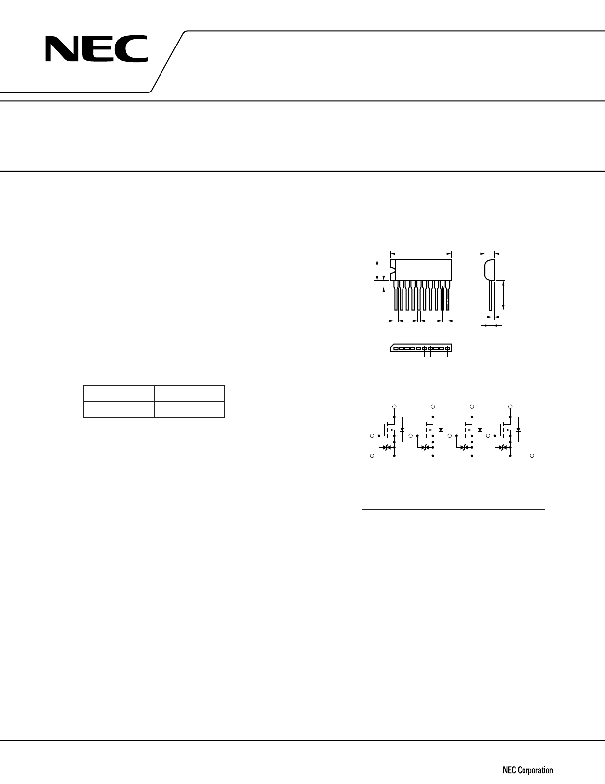
P-CHANNEL POWER MOS FET ARRAY
SWITCHING
INDUSTRIAL USE
DESCRIPTION
The µPA1523B is P-channel Power MOS FET Array that built
in 4 circuits designed for solenoid, motor and lamp driver.
µ
PA1523B
PACKAGE DIMENSIONS
in millimeters
FEATURES
• Full Mold Package with 4 Circuits
• –4 V driving is possible
• Low On-state Resistance
DS(on)1 = 0.8 Ω MAX. (@VGS = –10 V, ID = –1 A)
R
DS(on)2 = 1.3 Ω MAX. (@VGS = –4 V, ID = –1 A)
R
• Low Input Capacitance Ciss = 190 pF TYP.
ORDERING INFORMATION
Type Number Package
µ
PA1523BH 10 Pin SIP
ABSOLUTE MAXIMUM RATINGS (TA = 25 ˚C)
Drain to Source Voltage (VGS = 0)
Gate to Source Voltage (VDS = 0)
Drain Current (DC) I
Drain Current (pulse) ID(pulse) *1 8.0 A/unit
Total Power Dissipation PT1 *2 28 W
Total Power Dissipation P
Channel Temperature TCH 150 ˚C
Storage Temperature Tstg –55 to + 150 ˚C
Single Avalanche Current I
Single Avalanche Energy EAS *4 0.4 mJ
VDSS –60 V
VGSS(AC) 20 V
D(DC) 2.0 A/unit
T2 *3 3.5 W
AS *4 –2.0 A
±
±
±
26.8 MAX.
10
2.5
1.4 0.6 ± 0.1
12345678910
2.54
CONNECTION DIAGRAM
3
2
1
5
4
6
ELECTRODE CONNECTION
2, 4, 6, 8
3, 5, 7, 9
1, 10
4.0
7
8
: Gate
: Drain
: Source
10 MIN.
1.4
0.5 ± 0.1
9
10
*1 PW ≤ 10
*3 4 Circuits, TA = 25 ˚C *4 Starting TCH = 25 ˚C, VDD = –30 V, VGS = –20 V → 0, RG = 25 Ω,
Document No. G11331EJ1V0DS00
Date Published May 1996 P
Printed in Japan
µ
In case high voltage over V
s, Duty Cycle ≤ 1% *2 4 Circuits, T C = 25 ˚C
L = 100 µH
Build-in Gate Diodes are for protection from static electricity in handing.
GSS is applied, please append gate protection circuits.
The information in this document is subject to change without notice.
©
1996

µ
ELECTRICAL CHARACTERISTICS (TA = 25 ˚C)
CHARACTERISTIC SYMBOL TEST CONDITIONS MIN. TYP. MAX. UNIT
Drain Leakage Current IDSS VDS = –60 V, VGS = 0 –10
Gate Leakage Current IGSS VGS = 20 V, VDS = 0 10
Gate Cutoff Voltage VGS(off) VDS = –10 V, ID = –1.0 mA –1.0 –2.0 V
Forward Transfer Admittance | Yfs |VDS = –10 V, ID = –1.0 A 0.8 S
Drain to Source ON-Resistance RDS(on)1 VGS = –10 V, ID = –1.0 A 0.5 0.8 Ω
Drain to Source ON-Resistance RDS(on)2 VGS = –4.0 V, ID = –1.0 A 0.8 1.3 Ω
Input Capacitance Ciss VDS = –10 V, VGS = 0, f = 1.0 MHz 190 pF
Output Capacitance Coss 115 pF
Reverse Transfer Capacitance Crss 43 pF
Turn-on Delay Time td(on) ID = –1.0 A, VGS(on) = –10 V, 8 ns
Rise Time tr VDD = –30 V, RL = 30 Ω 53 ns
Turn-off Delay Time td(off) 400 ns
Fall Time tf 230 ns
Total Gate Charge QG VGS = –10 V, ID = –2.0 A, VDD = –48 V 10 nC
Gate to Source Charge QGS 1.1 nC
Gate to Drain Charge QGD 3.5 nC
Body Diode Forward Voltage VF(S-D) IF = 2.0 A, VGS = 0 1.0 V
Reverse Recovery Time trr IF = 2.0 A, VGS = 0, di/dt = 50 A/µs 180 ns
Reverse Recovery Charge Qrr 250 nC
±
.
.
±
PA1523B
µ
A
µ
A
2
Test Circuit 1 Avalanche Capability
R
G
= 25 Ω
D.U.T.
µ
PA1523B
L
Test Circuit 2 Switching Time
R
PG.
V
GS
0
t = 1 s
µ
Duty cycle ≤ 1 %
RG = 10 Ω
t
V
GS
= –20 V → 0
D.U.T.
G
PG.
50 Ω
BV
DSS
I
AS
I
D
V
DD
R
L
VGS
Wave
V
Form
DD
I
D
Wave
V
GS
0
(—)
I
D
0
Form
V
V
DS
Starting T
10 %
10 %
t
d(on)
DD
t
on
CH
90 %
V
GS(on)
90 %
90 %
I
D
t
r
t
d(off)
10 %
t
f
t
off
Test Circuit 3 Gate Charge
PG.
I
G
= 2 mA
50 Ω
D.U.T.
L
R
V
DD
3
TYPICAL CHARACTERISTICS (TA = 25 ˚C)
µ
PA1523B
TOTAL POWER DISSIPATION vs.
AMBIENT TEMPERATURE
3.5
3.0
2.5
2.0
1.5
µ
PA1523BH
0
NEC
Lead
Print
Circuit
Boad
50 100 150
1.0
- Total Power Dissipation - W
0.5
T
P
4 Circuits operation
3 Circuits operation
2 Circuits operation
1 Circuit operation
TA - Ambient Temperature - ˚C
FORWARD BIAS SAFE OPERATING AREA
–100
–10
= –10 V)
GS
I
D(DC)
I
D(Pulse)
Power Dissipation Limited
–1.0
- Drain Current - A
D
I
R
DS(on)
Limited(V
DC
TC = 25 ˚C
Single Pulse
–0.1
–0.1
–1.0 –10 –100
DS -
Drain to Source Voltage - V
V
FORWARD TRANSFER CHARACTERISTICS
–10
Under Same
dissipation in
each circuit
Pw = 100 s
500 s
µ
1 ms
10 ms
TOTAL POWER DISSIPATION vs.
CASE TEMPERATURE
30
Tc is grease
Temperature
on back surface
Under Same
dissipation in
each circuit
4 Circuits operation
20
3 Circuits operation
2 Circuits operation
1 Circuit operation
10
- Total Power Dissipation - W
T
P
0
50
100 150
TC - Case Temperature - ˚C
DERATING FACTOR OF FORWARD BIAS
SAFE OPERATING AREA
100
80
µ
60
40
20
dT - Percentage of Rated Power - %
0
20 40 60 80 100 120 140 160
C
- Case Temperature - ˚C
T
DRAIN CURRENT vs.
–8
DRAIN TO SOURCE VOLTAGE
Pulsed
–1
–0.1
- Drain Current - A
D
I
–0.01
0
4
TA=125 ˚C
75 ˚C
25 ˚C
–25 ˚C
–2 –6
GS
V
–4 –8
- Gate to Source Voltage - V
Pulsed
VDS = –10 V
–10
–6
VGS = – 10 V
–4
- Drain Current - A
D
–2
I
0
DS
- Drain to Source Voltage - V
V
–2
VGS = –4 V
–4
–6

1 000
100
TRANSIENT THERMAL RESISTANCE vs. PULSE WIDTH
Rth(CH-A) 4ircuits
3ircuits
2ircuits
1ircuit
µ
PA1523B
10
1.0
rth(t) - Transient Thermal Resistance - ˚C/W
0.1
FORWARD TRANSFER ADMITTANCE vs.
DRAIN CURRENT
100
10
TA = –25 ˚C
25 ˚C
75 ˚C
1.0
125 ˚C
µ
DS
= –
V
Pulsed
100 m
PW - Pulse Width - s
10 V
Rth(CH-C)
Single Pulse
1 10 1 000
DRAIN TO SOURCE ON-STATE RESISTANCE vs.
GATE TO SOURCE VOLTAGE
1.5
1.0
0.5
10010 m1 m100
ID = –2 A
–1 A
–0.4 A
Pulsed
0.1
| yfs | - Forward Transfer Admittance - S
–0.01
DRAIN TO SOURCE ON-STATE
RESISTANCE vs. DRAIN CURRENT
1 500
1 000
500
0
RDS(on) - Drain to Source On-State Resistance - mΩ
–0.1
I
D - Drain Current - A
ID - Drain Current - A
–1.0 –10
Pulsed
VGS = –4 V
VGS = –10 V
–1.0
0
RDS(on) - Drain to Source On-State Resistance - Ω
–2
–1
–10–0.1
VGS(off) - Gate to Source Cutoff Voltage - V
VGS - Gate to Source Voltage - V
GATE TO SOURCE CUTOFF VOLTAGE vs.
CHANNEL TEMPERATURE
0
–50
T
CH - Channel Temperature - ˚C
–10
VDS = –10 V
I
D = –1 mA
0 50 100 150
–20
5

µ
PA1523B
DRAIN TO SOURCE ON-STATE RESISTANCE vs.
CHANNEL TEMPERATURE
1600
1200
800
VGS = –4 V
VGS = –10 V
400
- Drain to Source On-State Resistance - mΩ
DS(on)
R
10 000
0
–50
0
T
CH
- Channel Temperature - ˚C
CAPACITANCE vs. DRAIN TO
SOURCE VOLTAGE
50
100 150
VGS = 0
f = 1 MHz
1 000
ID = –1 A
SOURCE TO DRAIN DIODE
FORWARD VOLTAGE
10
1.0
- Diode Forward Current - A
0.1
SD
I
VGS = –2 V
0
V
SD
- Source to Drain Voltage - V
SWITCHING CHARACTERISTICS
1 000
100
VGS=0
Pulsed
1.0 2.0
t
d(off)
t
f
- Capacitance - pF
rss
100
, C
oss
, C
iss
C
10
–0.1
1 000
–1 –10 –100
DS
- Drain to Source Voltage - V
V
REVERSE RECOVERY TIME vs.
DRAIN CURRENT
di/dt = 50A/ s
GS
= 0
V
100
- Reverse Recovery time - ns
rr
t
10
–0.1 –1.0 –10
I
D
- Drain Current - A
t
r
C
iss
C
oss
C
rss
- Switching Time - ns
f
, t
10
d(off)
, t
r
, t
d(on)
t
1.0
–0.01 –1.0 –10
t
d(on)
–0.1
I
D
- Drain Current - A
V
V
R
DD
= –30 V
GS
= –10 V
G
= 10 Ω
DYNAMIC INPUT/OUTPUT CHARACTERISTICS
µ
–60
VDD = –12 V
–40
–30 V
–48 V
ID = –2 A
V
–80
–16
–14
GS
–12
–10
–8
–6
–20
- Drain to Source Voltage - V
DS
V
V
DS
0426081210
Q
G
- Gate Charge - nC
–4
- Gate to Source Voltage - V
–2
GS
V
0
6

µ
PA1523B
SINGLE AVALANCHE ENERGY
DERATING FACTOR
100
80
60
VDD = –30 V
R
G
= 25 Ω
V
GS
= –20 V → 0
I
AS
≤ 1.0 A
–10
–1.0
SINGLE AVALANCHE CURRENT vs.
INDUCTIVE LOAD
IAS = –2 A
E
AS
= 0.4 mJ
40
–0.1
VDD = –30 V
- Single Avalanche Current - A
AS
I
VGS = –20 V → 0
G
= 25 Ω
R
Starting TCH = 25 ˚C
–0.1
µµ
10
100 1 m
L - Inductive Load - H
10 m
20
Energy Derating Factor - %
0
25
Starting T
50 75 100 125 150
CH
- Starting Channel Temperature - ˚C
REFERENCE
Document Name Document No.
NEC semiconductor for device reliability/quality control system TEI-1202
Quality grade on NEC semiconductor devices IEI-1209
Semiconductor device mounting technology manual C10535E
Semiconductor device package manual C10943X
Guide to quality assurance for semiconductor devices MEI-1202
Semiconductor selection guide X10679E
Power MOS FET features and application switching power supply TEA-1034
Application circuits using Power MOS FET TEA-1035
Safe operating area of Power MOS FET TEA-1037
7

µ
PA1523B
[MEMO]
No part of this document may be copied or reproduced in any form or by any means without the prior written
consent of NEC Corporation. NEC Corporation assumes no responsibility for any errors which may appear in this
document.
NEC Corporation does not assume any liability for infringement of patents, copyrights or other intellectual
property rights of third parties by or arising from use of a device described herein or any other liability arising
from use of such device. No license, either express, implied or otherwise, is granted under any patents,
copyrights or other intellectual property rights of NEC Corporation or others.
While NEC Corporation has been making continuous effort to enhance the reliability of its semiconductor devices,
the possibility of defects cannot be eliminated entirely. To minimize risks of damage or injury to persons or
property arising from a defect in an NEC semiconductor device, customer must incorporate sufficient safety
measures in its design, such as redundancy, fire-containment, and anti-failure features.
NEC devices are classified into the following three quality grades:
“Standard“, “Special“, and “Specific“. The Specific quality grade applies only to devices developed based on
a customer designated “quality assurance program“ for a specific application. The recommended applications
of a device depend on its quality grade, as indicated below. Customers must check the quality grade of each
device before using it in a particular application.
Standard: Computers, office equipment, communications equipment, test and measurement equipment,
audio and visual equipment, home electronic appliances, machine tools, personal electronic
equipment and industrial robots
Special: Transportation equipment (automobiles, trains, ships, etc.), traffic control systems, anti-disaster
systems, anti-crime systems, safety equipment and medical equipment (not specifically designed
for life support)
Specific: Aircrafts, aerospace equipment, submersible repeaters, nuclear reactor control systems, life
support systems or medical equipment for life support, etc.
The quality grade of NEC devices in “Standard“ unless otherwise specified in NEC's Data Sheets or Data Books.
If customers intend to use NEC devices for applications other than those specified for Standard quality grade,
they should contact NEC Sales Representative in advance.
Anti-radioactive design is not implemented in this product.
M4 94.11
 Loading...