

NEC UPA1728 Datasheet
DATA SHEET
MOS FIELD EFFECT TRANSISTOR
SWITCHING
N-CHANNEL POWER MOS FET
INDUSTRIAL USE
PA1728
µµµµ
DESCRIPTION
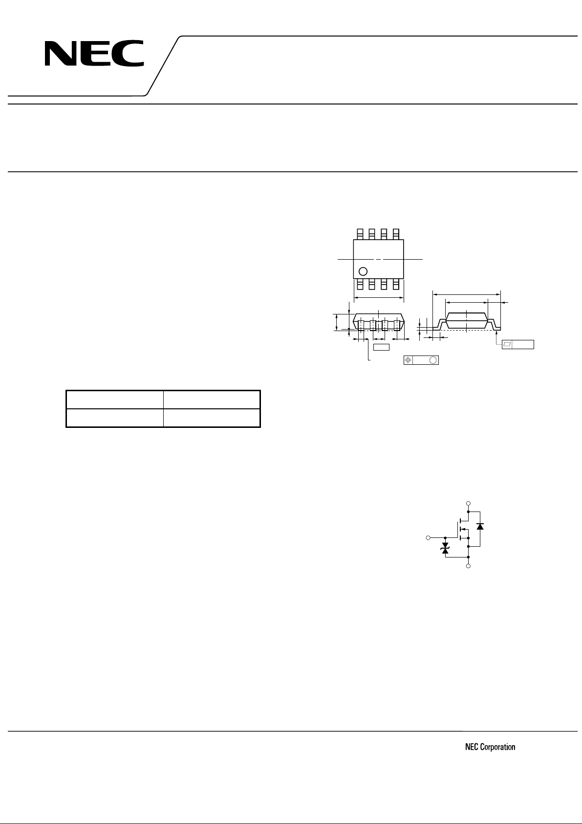
PACKAGE DRAWING (Unit : mm)
The µPA1728 is N-Channel MOS Field Effect Transistor
designed for high current switching applications.
85
FEATURES
Single chip type
•
Low On-state Resistance
•
★
★
★
★
DS(on)1
R
= 19 mΩ (TYP.) (VGS = 10 V, ID = 4.5 A)
DS(on)2
R
= 23 mΩ (TYP.) (VGS = 4.5 V, ID = 4.5 A)
DS(on)3
R
= 24 mΩ (TYP.) (VGS = 4.0 V, ID = 4.5 A)
iss
Low C
•
Built-in G-S protection diode
•
Small and surface mount package (Power SOP8)
•
iss
: C
= 1700 pF (TYP.)
14
1.44
1.8 Max.
0.05 Min.
ORDERING INFORMATION
PART NUMBER PACKAGE
PA1728 Power SOP8
µ
ABSOLUTE MAXIMUM RATINGS (TA = 25 °C, All terminals are connected.)
Drain to Source Voltage (VGS = 0 V) V
Gate to Source Voltage (V
DS
= 0 V) V
Drain Current (DC) I
Drain Current (Pulse)
Total Power Dissipation (T
Note1
A
= 25 °C)
Note2
Channel Temperature T
Storage Temperature T
Single Avalanche Current
Single Avalanche Energy
Notes 1.
★
PW ≤ 10
2.
Mounted on ceramic substrate of 1200 mm2 x 2.2 mm
3.
Starting Tch = 25°C, RG = 25 Ω, T
Note3
Note3
s, Duty cycle ≤ 1 %
µ
DSS
GSS
D(DC)
D(pulse)
I
T
P
ch
stg
AS
I
AS
E
GS
= 20 V →0 V
60 V
±20 V
±9 A
±36 A
2.0 W
150 °C
–55 to + 150 °C
9A
8.1 mJ
5.37 Max.
1.27
0.40
1, 2, 3
4
5, 6, 7, 8
6.0 ±0.3
4.4
+0.10
–0.05
0.78 Max.
+0.10
–0.05
0.15
0.12 M
0.5 ±0.2
EQUIVALENT CIRCUIT
Drain
Gate
Gate
Protection
Diode
Source
; Source
; Gate
; Drain
0.8
0.10
Body
Diode
Remark
The diode connected between the gate and source of the transistor serves as a protector against ESD.
When this device actually used, an additional protection circuit is externally required if a voltage
Exceeding the rated voltage may be applied to this device.
The information in this document is subject to change without notice. Before using this document, please
confirm that this is the latest version.
Not all devices/types available in every country. Please check with local NEC representative for
availability and additional information.
Document No. G14321EJ1V0DS00 (1st edition)
Date Published January 2000 NS CP(K)
Printed in Japan
The mark ★ shows major revised points.
©
1999,2000
★
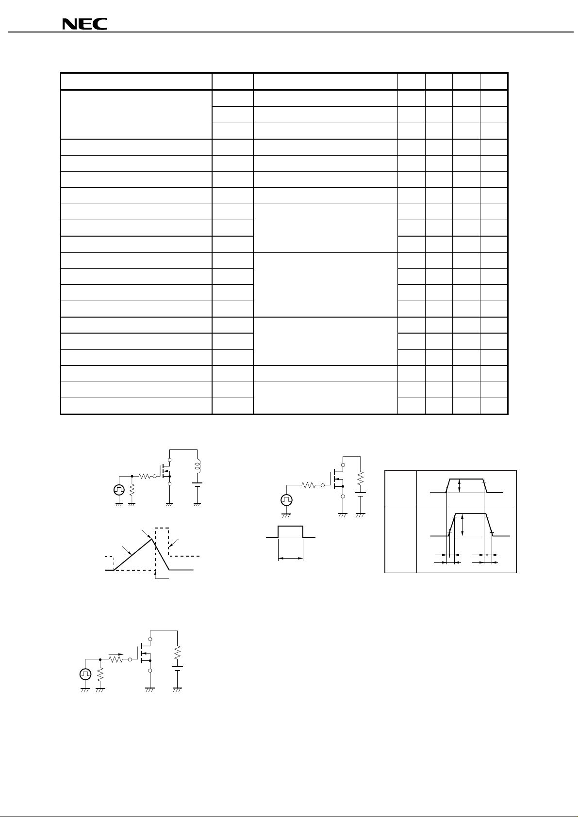
ELECTRICAL CHARACTERISTICS (TA = 25 °C, All terminals are connected.)
CHARACTERISTICS SYMBOL TEST CONDITIONS MIN. TYP. MAX. UNIT
µµµµ
PA1728
Drain to Source On-state Resi stance R
Gate to Source Cut-off Voltage V
DS(on)1VGS
DS(on)2VGS
R
DS(on)3VGS
R
GS(off)VDS
= 10 V, ID = 4.5 A 19 26 m
= 4.5 V, ID = 4.5 A 23 29 m
= 4.0 V, ID = 4.5 A 24 34 m
= 10 V, ID = 1 mA 1.5 2.0 2.5 V
Forward Transfer Admittance | yfs |VDS = 10 V, ID = 4.5 A 6.0 12 S
Drain Leakage Current I
Gate to Source Leakage Current I
Input Capacitance C
Output Capacitance C
Reverse Transfer Capacitance C
Turn-on Delay Time t
Rise Time t
Turn-off Delay Time t
Fall Time t
Total Gate Charge Q
Gate to Source Charge Q
Gate to Drain Charge Q
Body Diode Forward Voltage V
Reverse Recovery Time t
Reverse Recovery Charge Q
DSS
VDS = 60 V, VGS = 0 V 10
GSS
VGS = ±20 V, VDS = 0 V ±10
iss
VDS = 10 V 1700 pF
oss
VGS = 0 V 270 pF
rss
f = 1 MHz 130 pF
d(on)ID
d(off)
GS
GD
F(S-D)IF
rr
= 4.5 A 17 ns
r
GS(on)
V
= 10 V 69 ns
VDD = 30 V 77 ns
f
RG = 10
G
ID = 9 A 31 nC
Ω
31 ns
VDD = 48 V 4.4 nC
VGS = 10 V 9.1 nC
= 9 A, VGS = 0 V 0.82 V
IF = 9 A, VGS = 0 V 41 ns
rr
di/dt = 100A/µs76nC
Ω
Ω
Ω
A
µ
A
µ
TEST CIRCUIT 1 AVALANCHE CAPABILITY
D.U.T.
L
V
DD
PG.
RG = 25 Ω
50 Ω
VGS = 20 → 0 V
BV
DSS
I
AS
V
I
D
V
DD
DS
Starting T
ch
TEST CIRCUIT 3 GATE CHARGE
D.U.T.
PG.
IG = 2 mA
50 Ω
R
L
V
DD
TEST CIRCUIT 2 SWITCHING TIME
D.U.T.
R
L
G
PG.
GS
V
0
τ = 1 s
Duty Cycle ≤ 1 %
R
V
DD
τ
µ
GS
V
Wave Form
I
D
Wave Form
V
GS
10 %
0
90 %
I
D
10 %
0
t
d(on)
r
t
on
t
90 %
V
GS
(on)
90 %
I
D
10 %
t
d(off)
t
f
t
off
2
Data Sheet G14321EJ1V0DS00
 Loading...