

NEC UPA1716 Datasheet

DATA SHEET
MOS FIELD EFFECT TRANSISTOR
PA1716
µ
µ
µ µ
SWITCHING
P-CHANNEL POWER MOS FET
INDUSTRIAL USE
DESCRIPTION
This product is P-Channel MOS Field Effect Transistor designed for DC/DC converters and power management
applications of notebook computers.
FEATURES
Low on-resistance
•
DS(on)1
R
= 12.5 mΩ TYP. (VGS = –10 V, ID = –4 A)
DS(on)2
R
= 17.0 mΩ TYP. (VGS = –4.5 V, ID = –4 A)
DS(on)3
R
= 19.0 mΩ TYP. (VGS = –4.0 V, ID = –4 A)
iss
Low C
•
Built-in G-S protection diode
•
Small and surface mount package (Power SOP8)
•
iss
: C
= 2100 pF TYP.
PACKAGE DRAWING (Unit : mm)
85
14
5.37 Max.
1.44
ORDERING INFORMATION
PART NUMBER PACKAGE
PA1716G Power SOP8
µ
1.8 Max.
0.05 Min.
1.27
0.40
0.78 Max.
+0.10
–0.05
ABSOLUTE MAXIMUM RATINGS (TA = 25°C, All terminals are connected.)
Drain to Source Voltage (VGS = 0 V) V
Gate to Source Voltage (V
DS
= 0 V) V
Drain Current (DC) I
Drain Current (pulse)
Total Power Dissipation (T
Note1
A
= 25°C)
Note2
Channel Temperature T
Storage Temperature T
DSS
GSS
D(DC)
D(pulse)
I
P
ch
stg
–30 V
20 V
#
8 A
#
32 A
#
T
2.0 W
150 °C
–55 to +150 °C
; Source
1,2,3
; Gate
4
; Drain
5,6,7,8
6.0 ±0.3
4.4
+0.10
–0.05
0.15
0.12 M
0.5 ±0.2
EQUIVARENT CIRCUIT
Gate
Gate
Protection
Diode
0.8
0.10
Drain
Body
Diode
Source
Notes 1.
Remark
PW ≤ 10
2.
Mounted on ceramic substrate of 1200 mm
The diode connected between the gate and source of the transistor serves as a protector against ESD.
s, Duty Cycle ≤ 1 %
µ
When this device actually used, an additional protection circuit is externally required if a voltage
exceeding the rated voltage may be applied to this device.
The information in this document is subject to change without notice. Before using this document, please
confirm that this is the latest version.
Not all devices/types available in every country. Please check with local NEC representative for
availability and additional information.
Document No. G13727EJ1V0DS00 (1st edition)
Date Published March 1999 NS CP(K)
Printed in Japan
2
x 1.0 mm
©
1998, 1999
ELECTRICAL CHARACTERISTICS (TA = 25 °C, All terminals are connected.)
CHARACTERISTICS SYMBOL TEST CONDITIONS MIN. TYP. MAX. UNIT
µµµµ
PA1716
DS(on)1
Drain to Source On-state Resi stance
Gate to Source Cut-off Voltage V
R
R
R
DS(on)2
DS(on)3
GS(off)
Forward Transfer Admittance | yfs |
Drain Leakage Current I
Gate to Source Leakage Current I
Input Capacitance C
Output Capacitance C
Reverse Transfer Capacitance C
Turn-on Delay Time t
Rise Time t
Turn-off Delay Time t
Fall Time t
DSS
GSS
iss
oss
rss
d(on)
r
d(off)
f
Total Gate Charge Q
Gate to Source Charge Q
Gate to Drain Charge Q
Body Diode Forward Voltage V
GS
GD
F(S-D)IF
VGS = –10 V, ID = –4.0 A
VGS = –4.5 V, ID = –4.0 A
VGS = –4.0 V, ID = –4.0 A
VDS = –10 V, ID = –1 mA
DS
= –10 V, ID = –4.0 A
V
1.0
–
714 S
12.5 16 m
17 23 m
19 26 m
1.6
–
VDS = –30 V, VGS = 0 V
VGS = 20 V, VDS = 0 V 10
#
G
VDS = –10 V
GS
= 0 V
V
f = 1 MHz
ID = –4.0 A
GS(on)
= –10 V
V
DD
= –15 V
V
G
= 10
R
Ω
ID = –8.0 A
DD
= –24 V
V
GS
= –10 V
V
2100 pF
700 pF
300 pF
30 ns
150 ns
120 ns
76 ns
40 nC
6nC
10 nC
= 8.0 A, VGS = 0 V 0.8 V
Ω
Ω
Ω
2.5
–
1
–
#
V
A
µ
A
µ
Reverse Recovery Time t
Reverse Recovery Charge Q
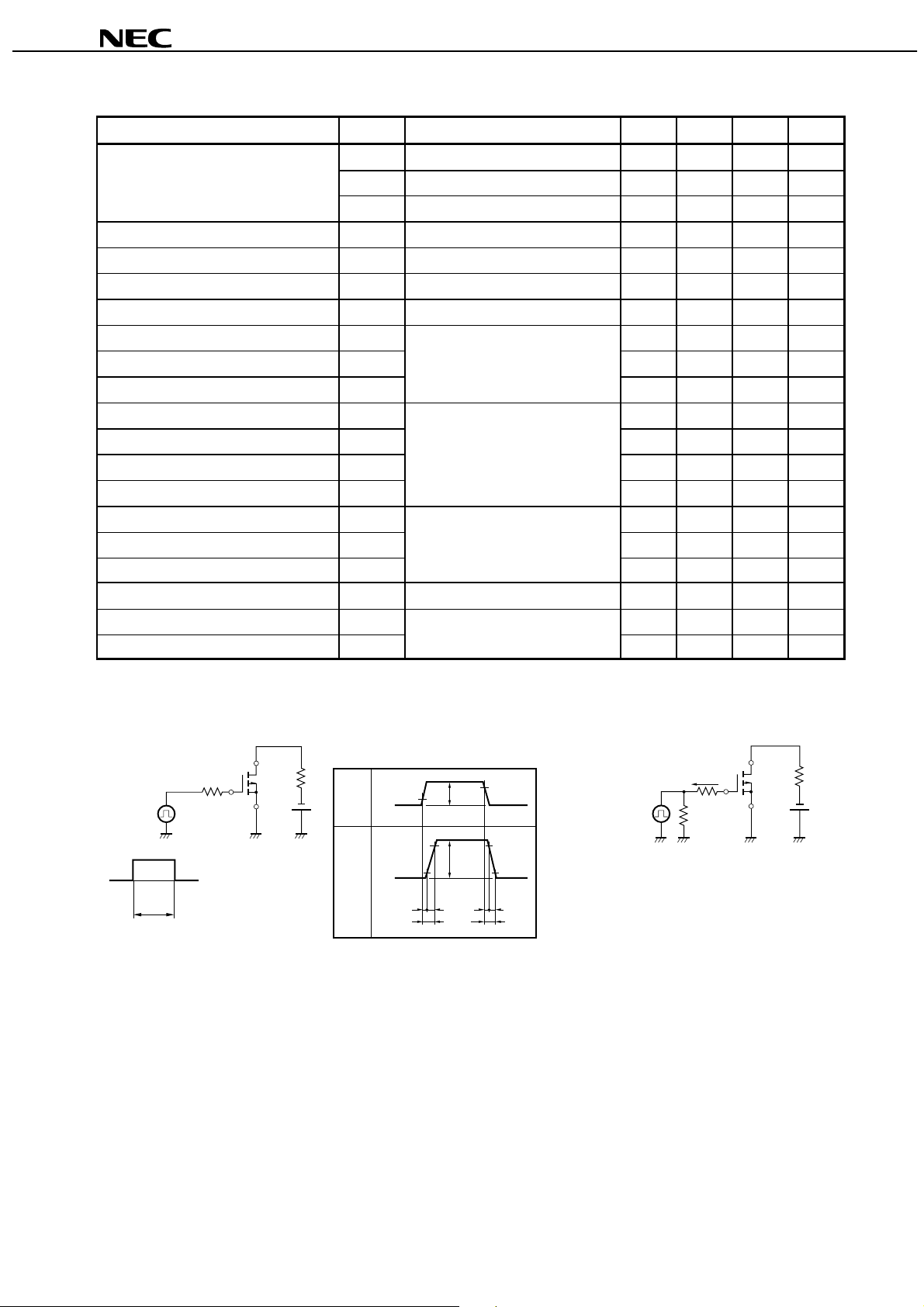
TEST CIRCUIT 1 SWITCHING TIME
D.U.T.
L
R
VGS
Wave Form
V
DD
ID
Wave Form
PG.
V
GS
0
=
1 µ s
τ
Duty Cycle ≤
τ
R
RG = 10 Ω
1
%
G
rr
IF = 8.0 A, VGS = 0 V
di/dt = 100 A/
rr
VGS
%
10
0
%
10
0
t
d (on)
90 %
ton toff
I
D
µ
90
VGS (on)
D
I
tr td (off) tf
s
%
90 %
10
45 ns
33 nC
TEST CIRCUIT 2 GATE CHARGE
D.U.T.
IG = 2 mA
Ω
PG.
%
50
R
L
V
DD
2
Data Sheet G13727EJ1V0DS00
TYPICAL CHARACTERISTICS (TA = 25 °C)
µ
µ
PA1716
µ µ
DERATING FACTOR OF FORWARD BIAS
SAFE OPERATING AREA
100
80
60
40
20
dT - Percentage of Rated Power - %
0
20 40 60 80 100 120 140 160
T
A
- Ambient Temperature - ˚C
FORWARD BIAS SAFE OPERATING AREA
−100
I
D(pulse)
100
ms
10
−10
ID(DC)
Power Dissipation Limited
ms
TOTAL POWER DISSIPATION vs.
AMBIENT TEMPERATURE
2.8
2.4
2.0
1.6
1.2
0.8
- Total Power Dissipation - W
T
0.4
P
0
20 40 60 80 100 120 140 160
T
A
- Ambient Temperature - ˚C
Remark
1
ms
1200 mm
Mounted on ceramic substrate of
2
x 1.0 mm
Mounted on ceramic
substrate of
2
1200mm x 1.0mm
−1
- Drain Current - A
D
I
TA = 25 ˚C
Single Pulse
−0.1
−0.1
V
DS -
1000
100
10
1
- Transient Thermal Resistance - ˚C/W
th(t)
r
0.1
µ
−1 −10 −100
Drain to Source Voltage - V
TRANSIENT THERMAL RESISTANCE vs. PULSE WIDTH
10
1 m
m
100
m
110
R
th(ch-A)
Mounted on ceramic
of
substrate
Single Pulse
1200 mm2 x 1.0 mm
= 62.5
˚C
1000100100
PW - Pulse Width - s
Data Sheet G13727EJ1V0DS00
3
 Loading...