

DATA SHEET
Compound Field Effect Power Transistor
N-CHANNEL POWER MOS FET ARRAY
SWITCHING
INDUSTRIAL USE
µ
PA1572B
DESCRIPTION
The µPA1572B is N-channel Power MOS FET Array
that built in 4 circuits designed for solenoid, motor and
lamp driver.
FEATURES
• Full Mold Package with 4 Circuits
• 4 V driving is possible
• Low On-state Resistance
R
DS(on) = 0.6 Ω MAX. (VGS = 10 V, ID = 1 A)
DS(on) = 0.8 Ω MAX. (VGS = 4 V, ID = 1 A)
R
• Low Input Capacitance Ciss = 110 pF TYP.
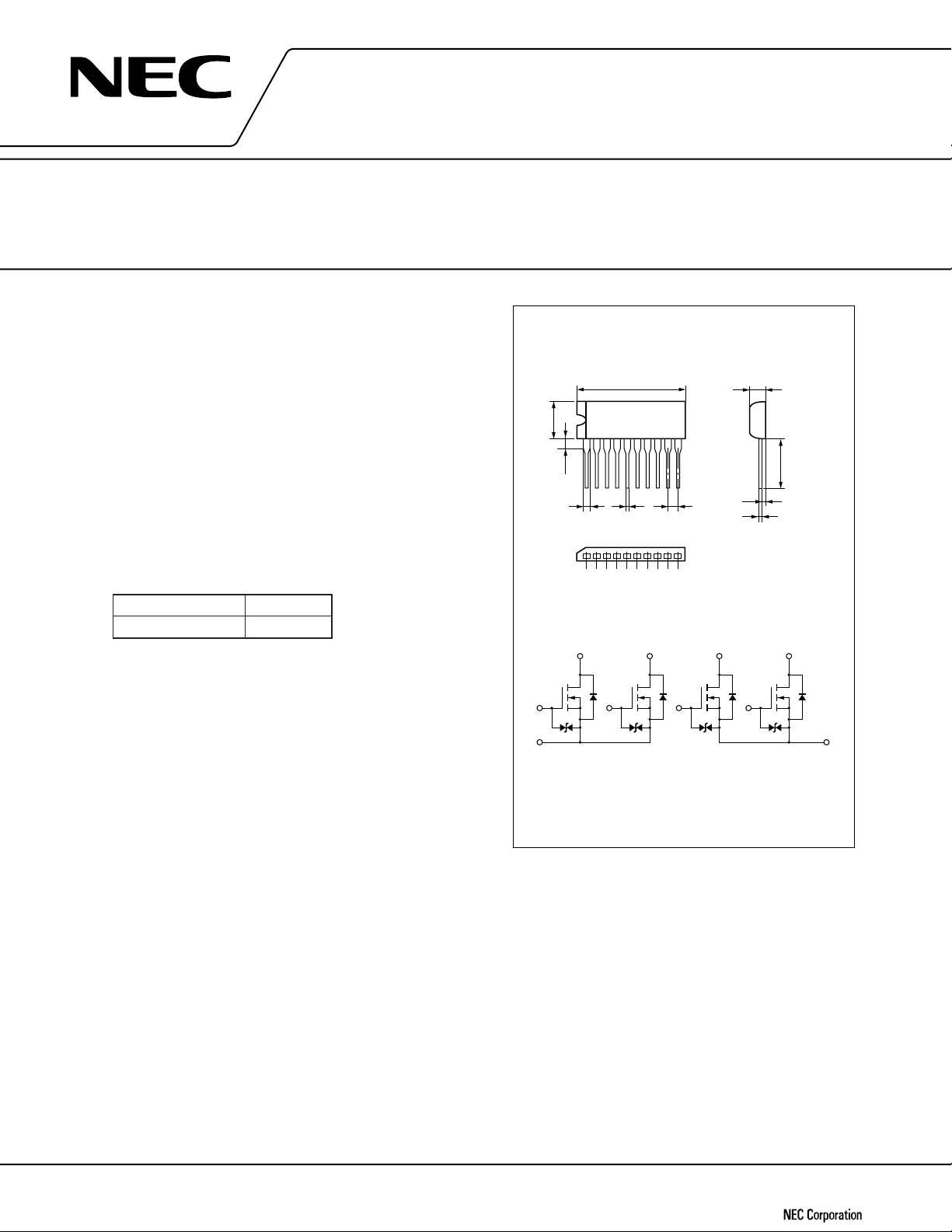
ORDERING INFORMATION
Type Number Package
µ
PA1572BH 10Pin SIP
PACKAGE DIMENSIONS
in millimeters
26.8 MAX.
10
2.5
1.4
12345678910
0.6±0.1
2.54
4.0
10 MIN.
1.4
0.5±0.1
CONNECTION DIAGRAM
3
2468
110
5
79
ABSOLUTE MAXIMUM RATINGS (TA = 25 °C)
Drain to Source Voltage (VGS = 0) VDSS 60 V
Gate to Source Voltage (V
Drain Current (DC) I
Drain Current (pulse) I
Total Power Dissipation P
Total Power Dissipation P
Channel Temperature T
Storage Tempreature T
Single Avalanche Current I
Single Avalanche Energy E
*1 PW ≤ 10 µs, Duty Cycle ≤ 1 % *2 4 Circuits TC = 25 °C
*3 4 Circuits T
A = 25 °C *4 Starting TCH = 25 °C, VDD = 30 V, VGS = 20 V → 0, RG = 25 Ω, L = 100
In case high voltage over V
Document No. G11177EJ1V0DS00 (1st edition)
Date Published May 1996 P
Printed in Japan
DS = 0) VGSS (AC) ±20 V
D (DS) ±2.0 A/unit
D (pulse) *1 ±6.0 A/unit
T1 *2 20 W
T2 *3 3.0 W
CH 150 °C
stg −55 to +150°C
AS *4 5.0 A
AS *4 0.1 mJ
Build-in Gate Diodes are for protection from static electricity in handing.
GSs is applied, please append gate protection circuits.
The information in this document is subject to change without notice.
ELECTRODE CONNECTION
2, 4, 6, 8
3, 5, 7, 9
1, 10
: Gate
: Drain
: Source
µ
H
©
1996
µ
PA1572B
ELECTRICAL CHARACTERISTICS (TA = 25 °C)
CHARACTERISTIC SYMBOL MIN. TYP. MAX. UNIT TEST CONDITION
Drain Leakage Current IDSS 10
Gate Leakage Current IGSS ±10
Gate Cutoff Voltage VGS (off) 1.0 2.0 V VDS = 10 V, ID = 1.0 mA
Forward Transfer Admittance
Drain to Source ON-Resistance RDS (on)1 0.3 0.6 Ω VGS = 10 V, ID = 1.0 A
Drain to Sourse ON-Resistance RDS (on)2 0.4 0.8 Ω VGS = 4.0 V, ID = 1.0 A
Input Capacitance Ciss 110 pF VDS = 10 V, VGS = 0, f = 1.0 MHz
Output Capacitance Coss 70 pF
Reverse Transfer Capacitance Crss 25 pF
Turn-on Delay Time td (on) 30 ns ID = 1.0 A, VGS (on) = 10 V, VDD = 30 V, RL = 30 Ω
Rise Time tr 200 ns
Turn-off Delay Time td (off) 100 ns
Fall Time tf 160 ns
Total Gate Charge QG 5.4 nC VGS = 10 V, ID = 2.0 A, VDD = 48 V
Gate to Source Charge QGS 0.7 nC
Gate to Drain Charge QGD 2.0 nC
Body Diode Forward Voltage VF (S-D) 1.0 V IF = 2.0 A, VGS = 0
Reverse Recovery Time trr 130 ns IF = 2.0 A, VGS = 0, di/dt = 50 A/µs
Reverse Recovery Charge Qrr 110 nC
Yfs
0.5 S VDS = 10 V, ID = 1.0 A
µ
AVDS = 60 V, VGS = 0
µ
AVGS = ±20 V, VDS = 0
2
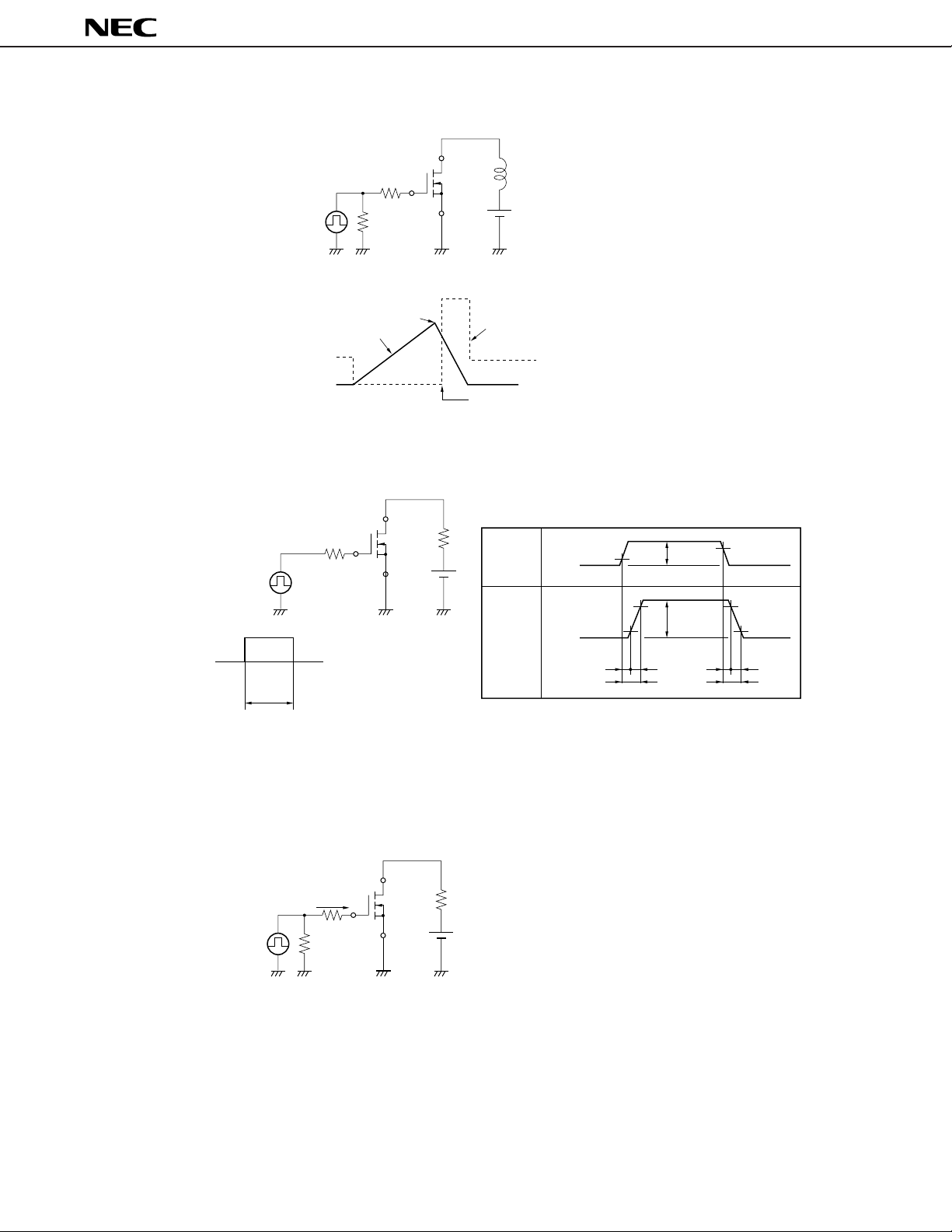
Test Circuit 1 Avalanche Capability
G
R
D.U.T.
= 25 Ω
µ
PA1572B
L
V
GS
= 20 V → 0
Test Circuit 2 Switching Time
PG.
V
GS
0
t
µ
t = 1 s
Duty Cycle ≤ 1 %
PG.
R
V
R
G
G
= 10 Ω
DD
D.U.T.
50 Ω
I
D
V
DD
BV
DSS
I
AS
V
DS
R
L
DD
V
Starting T
V
GS
Wave From
I
D
Wave From
CH
V
GS
V
10 %
0
10 %
t
d (on)
90 %
t
on
I
D
0
GS (on)
I
D
t
r
t
d (off)
90 %
t
off
90 %
10 %
t
r
Test Circuit 3 Gate Charge
PG.
G
= 2 mA
I
50 Ω
D.U.T.
R
L
DD
V
3
 Loading...