

Motorola SN54LS75AJ, SN54LS77AJ, SN74LS77AD, SN74LS77AN, SN74LS75AN Datasheet
NOTES:
tn = bit time before enable
negative-going transition
t
n+1
= bit time after enable
negative-going transition
5-75
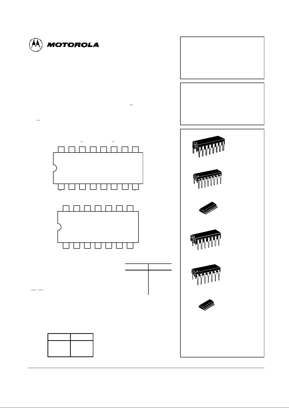
FAST AND LS TTL DATA
4-BIT D LATCH
The TTL/MSI SN54/74LS75 and SN54/74LS77 are latches used as temporary storage for binary information between processing units and input/output or indicator units. Information present at a data (D) input is transferred to
the Q output when the Enable is HIGH and the Q output will follow the data
input as long as the Enable remains HIGH. When the Enable goes LOW, the
information (that was present at the data input at the time the transition occurred) is retained at the Q output until the Enable is permitted to go HIGH.
The SN54/74LS75 features complementary Q and Q
output from a 4-bit
latch and is available in the 16-pin packages. For higher component density
applications the SN54/74LS77 4-bit latch is available in the 14-pin package
with Q
outputs omitted.
14 13 12 11 10 9
1 2 3 4 5 6
7
16 15
8
CONNECTION DIAGRAMS DIP (TOP VIEW)
SN54/74LS75
14 13 12 11 10 9
1 2 3 4 5 6
8
7
SN54/74LS77
Q
0
Q
0
Q1Q
1E0–1
GND Q
2
Q
2
Q
3
D0D1E
2–3VCCD2D3
Q
3
Q0Q1E
0–1
GND NC Q2Q
3
D0D1E
2–3VCCD2D3
NC
PIN NAMES LOADING (Note a)
HIGH
LOW
D1–D
4
E
0–1
E
2–3
Q1–Q
4
Q
1–Q4
Data Inputs
Enable Input Latches 0, 1
Enable Input Latches 2, 3
Latch Outputs (Note b)
Complimentary Latch Outputs (Note b)
0.5 U.L.
2.0 U.L.
2.0 U.L.
10 U.L.
10 U.L.
0.25 U.L.
1.0 U.L.
1.0 U.L.
5 (2.5) U.L.
5 (2.5) U.L.
NOTES:
a) 1 Unit Load (U.L.) = 40 µA HIGH.
b) The Output LOW drive factor is 2.5 U.L. for Military (54) and 5 U.L. for Commercial (74)
Temperature Ranges.
TRUTH TABLE
(Each latch)
t
n
t
n+1
D
H
L
Q
H
L
SN54/74LS75
SN54/74LS77
4-BIT D LATCH
LOW POWER SCHOTTKY
J SUFFIX
CERAMIC
CASE 620-09
N SUFFIX
PLASTIC
CASE 648-08
16
1
16
1
ORDERING INFORMATION
SN54LSXXJ Ceramic
SN74LSXXN Plastic
SN74LSXXD SOIC
16
1
D SUFFIX
SOIC
CASE 751B-03
J SUFFIX
CERAMIC
CASE 632-08
N SUFFIX
PLASTIC
CASE 646-06
14
1
14
1
14
1
D SUFFIX
SOIC
CASE 751A-02
5-76
FAST AND LS TTL DATA
SN54/74LS75
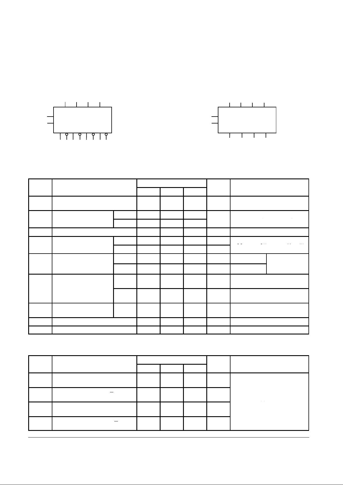
LOGIC SYMBOLS
VCC = PIN 5
GND = PIN 12
2 3 6 7
16 1 15 14 10 11 9 8
D0D1D2D
3
13
4
E
0–1
E
2–3
Q0Q1Q2Q
3
Q
0
Q1Q
2
Q
3
SN54/74LS75
VCC = PIN 4
GND = PIN 11
NC = PIN 7, 10
1 2 5 6
14 13 9 8
D0D1D2D
3
12
3
E
0–1
E
2–3
Q
0
Q
3
Q1Q
2
SN54/74LS77
DC CHARACTERISTICS OVER OPERATING TEMPERATURE RANGE
(unless otherwise specified)
Limits
Symbol
Parameter
Min Typ Max
Unit
Test Conditions
V
IH
Input HIGH Voltage 2.0 V
Guaranteed Input HIGH Voltage for
All Inputs
54 0.7
Guaranteed Input LOW Voltage for
VILInput LOW Voltage
74 0.8
V
Guaranteed Input LOW Voltage for
All Inputs
V
IK
Input Clamp Diode Voltage –0.65 –1.5 V VCC = MIN, IIN = –18 mA
54 2.5 3.5 V
V
CC
= MIN, IOH = MAX, VIN = V
IH
VOHOutput HIGH Voltage
74 2.7 3.5 V
VCC = MIN, IOH = MAX, VIN = V
IH
or VIL per Truth Table
54, 74 0.25 0.4 V IOL = 4.0 mA
VCC = VCC MIN,
VOLOutput LOW Voltage
74 0.35 0.5 V IOL = 8.0 mA
VIN = VIL or V
IH
per Truth Table
D Input
E Input
20
80
µA VCC = MAX, VIN = 2.7 V
IIHInput HIGH Current
D Input
E Input
0.1
0.4
mA VCC = MAX, VIN = 7.0 V
I
IL
Input LOW Current
D Input
E Input
–0.4
–1.6
mA VCC = MAX, VIN = 0.4 V
I
OS
Short Circuit Current (Note 1) –20 –100 mA VCC = MAX
I
CC
Power Supply Current 12 mA VCC = MAX
Note 1: Not more than one output should be shorted at a time, nor for more than 1 second.
AC CHARACTERISTICS (T
A
= 25°C, VCC = 5.0 V)
Limits
Symbol
Parameter
Min Typ Max
Unit
Test Conditions
t
PLH
t
PHL
Propagation Delay, Data to Q
15
9.0
27
17
ns
t
PLH
t
PHL
Propagation Delay, Data to Q
12
7.0
20
15
ns
V
CC
= 5.0 V
t
PLH
t
PHL
Propagation Delay, Enable to Q
15
14
27
25
ns
VCC = 5.0 V
CL = 15 pF
t
PLH
t
PHL
Propagation Delay, Enable to Q
16
7.0
30
15
ns
 Loading...