

Motorola MC100SX1452FI Datasheet
MCM6341
1
MOTOROLA FAST SRAM
Advance Information
128K x 24 Bit Static Random
Access Memory
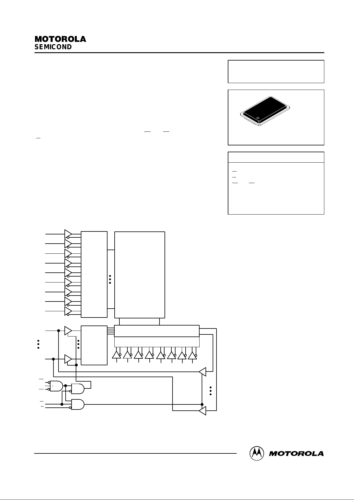
The MCM6341 is a 3,145,728–bit static random access memory organized as
131,072 words of 24 bits. Static design eliminates the need for external clocks
or timing strobes.
The MCM6341 is equipped with chip enable (E1
, E2, E3) and output enable
(G
) pins, allowing for greater system flexibility and eliminating bus contention
problems.
The MCM6341 is available in a 119–bump PBGA package.
• Single 3.3 V ± 10% Power Supply
• Fast Access Time: 10/11/12/15 ns
• Equal Address and Chip Enable Access Time
• All Inputs and Outputs are TTL Compatible
• Three–State Outputs
• Power Operation: 280/275/270/260 mA Maximum, Active AC
• Commercial Temperature (0°C to 70°C) and
Industrial Temperature (– 40°C to + 85°C) Options
DQ
BLOCK DIAGRAM
G
AAAAAAAA
MEMORY MATRIX
ROW
DECODER
INPUT
DATA
CONTROL
A
A
A
A
A
A
A
DQ
E1
W
A
A
COLUMN I/O
COLUMN DECODER
DQ
DQ
E2
E3
This document contains information on a new product. Specifications and information herein are subject to change without notice.
Order this document
by MCM6341/D
MOTOROLA
SEMICONDUCTOR TECHNICAL DATA
MCM6341
A Address Inputs. . . . . . . . . . . . . . . . . . . . . .
W
Write Enable. . . . . . . . . . . . . . . . . . . . . . .
G
Output Enable. . . . . . . . . . . . . . . . . . . . .
E1
, E2, E3 Chip Enable. . . . . . . . . . . . . . . .
DQ Data Input/Output. . . . . . . . . . . . . . . . .
NC No Connection. . . . . . . . . . . . . . . . . . . .
V
DD
+ 3.3 V Power Supply. . . . . . . . . . . . .
V
SS
Ground. . . . . . . . . . . . . . . . . . . . . . . . .
PIN NAMES
ZP PACKAGE
PBGA
CASE 999–02
REV 2
2/18/98
Motorola, Inc. 1998
MCM6341
2
MOTOROLA FAST SRAM
PIN ASSIGNMENT
119–BUMP PBGA
TOP VIEW
6543217
B
C
V
SS
G
A
D
E
F
H
J
V
DD
V
SS
V
DD
V
SS
A
V
SS
V
SS
AA AA
NC
AA AA
NC
DQ
DQ
NC NC
A
NC
V
DD
DQ
NCNC
A
W
AA
NC
G
DQ V
SS
NC
V
DD
DQ
DQ V
SS
DQ
V
DD
DQ
DQ V
SS
V
SS
DQ
V
DD
V
DD
V
SS
V
DD
V
SS
DQ
DQ VDDV
SS
V
SS
V
SS
V
DD
V
SS
DQ
DQ VDDVSSV
SS
V
DD
DQ
NC A A E1
K
L
M
N
P
R
T
U
NC NC
A
NC NC
DQ
V
SS
V
DD
V
DD
V
DD
V
DD
V
SS
V
SS
V
DD
E2 NC E3
NC
A
V
SS
V
SS
V
SS
V
SS
V
SS
V
SS
V
SS
V
SS
V
SS
V
DD
V
DD
V
DD
V
SS
V
SS
V
DD
V
DD
V
DD
V
DD
V
SS
V
SS
DQ
DQ
DQ
DQ
DQ
DQ
DQ
DQ
MCM6341
3
MOTOROLA FAST SRAM
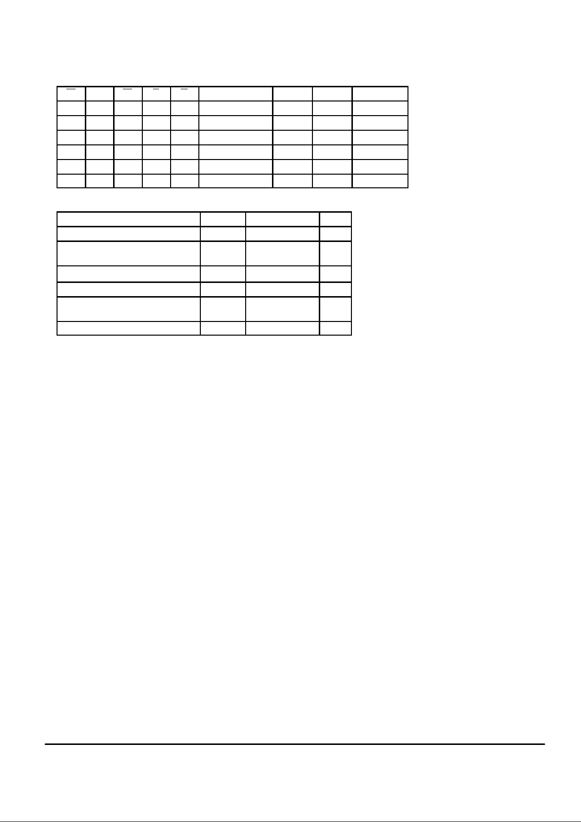
TRUTH TABLE (X = Don’t Care)
E1 E2 E3 G W Mode I/O Pin Cycle Current
H X X X X Not Selected High–Z — I
SB1
, I
SB2
X L X X X Not Selected High–Z — I
SB1
, I
SB2
X X H X X Not Selected High–Z — I
SB1
, I
SB2
L H L H H Output Disabled High–Z — I
DDA
L H L L H Read D
out
Read I
DDA
L H L X L Write High–Z Write I
DDA
ABSOLUTE MAXIMUM RATINGS (See Note)
Rating
Symbol Value Unit
Power Supply Voltage Relative to V
SS
V
DD
– 0.5 to + 5.0 V
Voltage Relative to VSS for Any Pin
Except V
DD
Vin, V
out
– 0.5 to VDD + 0.5 V
Output Current (per I/O) I
out
± 20
mA
Power Dissipation P
D
1.0 W
Temperature Under Bias Commercial
Industrial
T
bias
– 10 to + 85
– 45 to + 90
°C
Storage Temperature — Plastic T
stg
– 55 to + 150 °C
NOTE: Permanent device damage may occur if ABSOLUTE MAXIMUM RATINGS are
exceeded. Functional operation should be restricted to RECOMMENDED OPERATING CONDITIONS. Exposure to higher than recommended voltages for
extended periods of time could affect device reliability.
This device contains circuitry to protect the
inputs against damage due to high static voltages or electric fields; however, it is advised
that normal precautions be taken to avoid application of any voltage higher than maximum
rated voltages to these high–impedance circuits.
This CMOS memory circuit has been
designed to meet the dc and ac specifications
shown in the tables, after thermal equilibrium
has been established. The circuit is in a test
socket or mounted on a printed circuit board and
transverse air flow of at least 500 linear feet per
minute is maintained.
 Loading...