

Motorola MC100SX1451FI100 Datasheet
SEMICONDUCTOR TECHNICAL DATA
1
REV 0
Motorola, Inc. 1997
7/97
!
The MC100SX1451FI100 AutoBahn chip is a high–speed serial–
to–parallel, parallel–to–serial transceiver. The AutoBahn can be used to
implement a high–speed, half–duplex, bi–directional serial data link with
an effective data transfer rate of 100MByte/sec. A higher performance
AutoBahn chip, with user selectable serial data transfer rates of 100 or
200MByte/s, is planned (see the MC100SX1451FI200 datasheet).This
serial link can be used to establish multi–point or point–to–point
connections. A unique differential cutoff driver switches from a standard
PECL VOH level to cutoff. In the cutoff state the outputs present a high
impedance which is required to implement a true shared bus. The part
features a 32–bit wide parallel TTL compatible I/O interface that can
connect directly with standard memory or bus transceiver devices. The
control pins are all TTL compatible to simplify interfacing requirements.
The serial interface is PECL (Positive Emitter Coupled Logic) which
provides excellent transmission line drive capability. Because the serial
bus is implemented using differential ECL technology, the receiver
circuitry exhibits excellent common mode noise rejection.
• 100MByte/s Serial Data Transfer Capability
• TTL Compatible Parallel Interface
• Supports 16– or 32–Bit Data Bus Interfaces
• Bus Driving Differential ECL Serial Outputs
• On–Board Clock Recovery and Data Synchronization
• 64–Pin Surface Mount CQFP Packaging
• Parallel Data Bus Handshake Control
An innovative data synchronizing architecture allows data to be transmitted in bursts without preamble bits. This allows
instantaneous data acquisition without the inherent overhead of traditional PLL clock recovery. Thus, the data transfer is nearly
overhead free with only one synchronization bit for every byte of data transmitted. Insertion and removal of synchronization bits
are totally transparent to the user.
The AutoBahn supports variable data transfer rates. This is accomplished by combining the fixed burst transfer rates of 50 or
100MByte/s with a flexible method of allowing data to be written into the AutoBahn for transfer. If new data has not been written
into the parallel data register prior to the completion of a serial data burst, the AutoBahn will insert a gap in the serial data stream.
Therefore, the effective throughput of the serial bus is throttled by the speed of the parallel host interface which writes data to the
chip.
With its very high block data transfer capability and instantaneous start up ability, the AutoBahn is ideally suited for multimedia
graphics applications and parallel processing architectures requiring multi–processor communication links.
Motorola’s state–of–the–art MOSAIC V process allows for the realization of 1.8GHz internal clock rates at power levels
which are compatible with today’s low profile surface mount packages. Furthermore, the design is implemented with a
flow–through pinout architecture to simplify PCB layout and routing. The board space efficiency of the CQFP ensures that the
AutoBahn device will prove valuable in the most demanding space conscious applications.
The AutoBahn chip works from a single +5.0V supply. Separate internal VCC busses isolate the TTL outputs from the high
speed PECL circuitry.
AutoBahn and Spanceiver are trademarks of PEP Modular Computers.
‘Spanceiver’ has been formed as a contraction of Serial/Parallel Transceiver .
MOSAIC V is a trademark of Motorola, Inc.
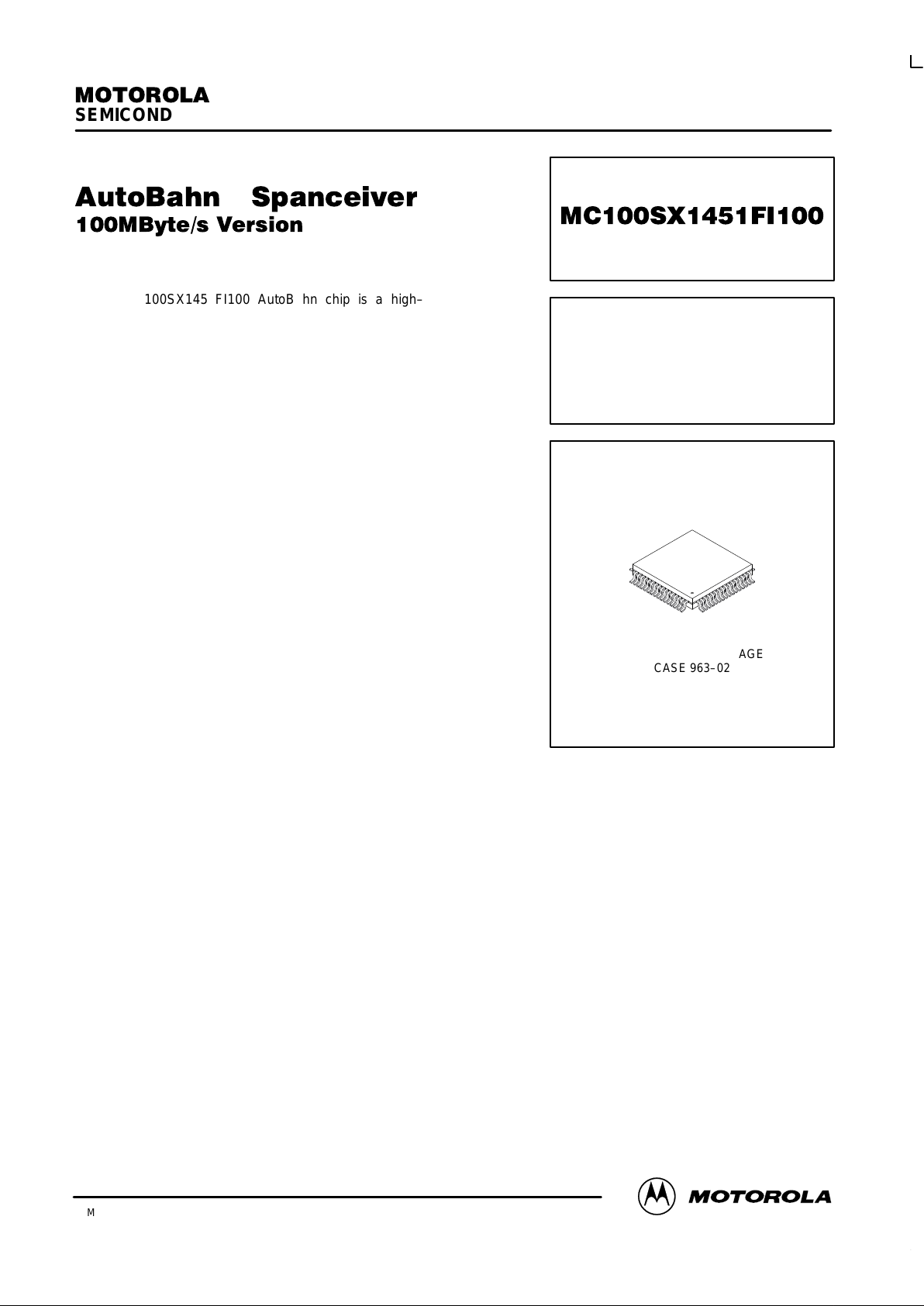
AUTOBAHN
SPANCEIVER
FI SUFFIX
CERAMIC QFP PACKAGE
CASE 963–02
MC100SX1451FI100
MOTOROLA ECLinPS and ECLinPS Lite
DL140 — Rev 3
2
CONTROL
REGISTER
ERROR
REGISTER
Figure 1. Simplified Block Diagram
TRANSMIT
REGISTER
PISO
SHIFT
REGISTER
SYNC
BIT
GENERATOR
RECEIVE
REGISTER
SIPO
SHIFT
REGISTER
SYNC
BIT
EXTRACT
PLL
CLOCK
GENERATOR
DIFFERENTIAL
DETECTOR
PISO
CONTROL
LOGIC
SIPO
CONTROL
LOGIC
SERIAL
BUS
TRANSCEIVER
FULL
BUSY
ERROR
FOSC
C1
D31–
D00
REGSEL
REGISTER
READ/
WRITE
LOGIC
RESET
LOGIC
R/W
STRB
RESET
SER
SER
MC100SX1451FI100
ECLinPS and ECLinPS Lite
DL140 — Rev 3
3 MOTOROLA
PIN DESCRIPTIONS
Name I/O Description
TTL COMPATIBLE I/O
RESET I Asynchronous reset signal which places the AutoBahn into default state. In most applications, RESET should
only have to be asserted on system startup.
R/W I Read/Write control signal. Used to select between writing to or reading from the AutoBahn.
REGSEL I Control signal used to select between the Parallel Data Register and the Control and Error Register(s). A logic
‘H’ selects the data register while a logic ‘L’ selects the Control and Error Register(s).
D00 – D31 I/O Bi–directional data inputs/outputs. These pins comprise the data bus to be used to interface to the user host
interface. D00 is the least significant bit.
STRB I Data strobe signal. During a write, it indicates that data is valid on the parallel bus. While in a read, it indicates
that the AutoBahn can now place data on the parallel interface.
FULL O Signal which indicates that the transmitter or receiver presently contains data. In conjunction with the STRB
signal, it is used to implement a two signal handshake for parallel data transfers.
BUSY O Serial bus BUSY signal, used to indicate to the parallel interface that the AutoBahn bus is presently in use.
ERROR O Control output which is used to indicate that the AutoBahn has identified a fault condition. The error condition
can then be read out from the Error Register.
FOSC I 25.00MHz clock source from a crystal oscillator reference.
PECL COMPATIBLE I/O
SER/SER I/O Differential serial data inputs/outputs which operate at modified PECL levels.
POWER, GROUND AND FILTER PINS
Name Number Description
C1 1 PLL Filter Capacitor Pin
V
CCE
1 Positive Supply for Internal PECL Logic Circuitry
V
CCO
1 Positive Supply for PECL Outputs
V
EE
1 Ground for PECL
V
CCT
7 Positive Supply for TTL Compatible Signals
V
EET
8 Ground for TTL Compatible Signals
V
CCX
1 Positive Supply for VCO
V
EEX
1 Ground for VCO
BLOCK DIAGRAM FUNCTIONAL DESCRIPTION
Reset Logic
The Reset Logic generates the internal reset signal used
to set the device into a known state. The reset signal clears
the Control and Error Registers and resets the SIPO and
PISO Control Logic. The external reset signal is validated
with the FOSC input clock to assure that a valid reset pulse
has been applied to the chip. The external reset input pin
(RESET
) must be low for a minimum of 125 nsec after the
FOSC input is stable. STRB
assertion may occur no earlier
than 500 nsec after RESET
deassertion (reset recovery
time).
Control Register
The Control Register is used to configure the operation of
the AutoBahn. The register fields are described in detail in
the section containing the Control and Error Register Bit
Definition.
Register Read/Write Control Logic
This logic is utilized to access the Transmit Register, the
Receive Register, and the Control and Error Registers from
the parallel bus. The interface protocol utilizes two direction
control signals (R/W
and REGSEL). The actual handshake to

MC100SX1451FI100
MOTOROLA ECLinPS and ECLinPS Lite
DL140 — Rev 3
4
read or write data from the chip is accomplished with the
input STRB
signal , combined with the output FULL signal.
Transmit Register
The transmit register is a 32–bit wide parallel–loadable
register. This register interfaces to the bi–directional TTL
compatible data bus. Access to this register is controlled via
the Register Read/Write Logic.
PISO Shift Register
The PISO (Parallel In/Serial Out) Register accepts data
from the Transmit Register and converts it into a serial bit
stream. This register is under control of the PISO Control
Logic. The shift register can be adjusted to handle 16–bit or
32–bit data traffic based on the state of the appropriate field
in the Control Register.
PISO Control Logic
The PISO (Parallel In/Serial Out) Control Logic is
responsible for controlling the transfer of data out from the
AutoBahn to the serial bus. This logic interfaces to the PISO
Shift Register and the SYNC Bit Generator. It is driven by the
PLL Clock Generator.
SYNC Bit Generator
This circuitry inserts one bit of timing information into the
data stream before every byte of data is sent to the Serial Bus
Transceiver and transmitted. This timing information is used
by the receiver to properly re–clock the incoming data
stream. T o support the maximum data rate of 100 MByte/sec,
the actual serial shift rate is 900 MBit/s NRZ, rather than
800 MBit/s NRZ. The insertion and removal of SYNC bits is
transparent to the end user.
Serial Bus Transceiver
The transceiver implements a two signal bi–directional
differential bus. The transceiver circuitry consists of a highly
sensitive differential receiver and a cutoff driver . The receiver
accepts a differential signal from the serial bus. This
differential signal is amplified and limited by the receiver
before being routed to the clock generation circuitry for clock
extraction and data re–timing.
The cutoff driver is used to transmit serial data on to the
bus. The outputs switch between a normal HIGH level (VOH)
and a cutoff LOW signal – when low the output emitter
follower is turned ’off’, thus presenting a high impedance to
the bus. If the cutoff driver is disabled, both outputs of the
differential pair go to the cutoff state so the bus resource is
available for use by other AutoBahn chips sharing the
same bus.
Differential Detector
The differential detector is used to recognize when the
serial bus goes out of the cutoff state and into a differential
steady state condition. The differential detector is only
utilized at the very start of a transmission. The detector
informs the SIPO Control Logic that the serial bus is no
longer in cutoff so that the bus BUSY
signal can be asserted
by the device.
PLL Clock Generator
The Clock Generator circuitry synthesizes a master timing
clock from the frequency reference signal (FOSC) input. The
clock generator provides timing signals used to support the
transfer rate of 900 MBit/s. The clock is generated by a
Phase Locked Loop (PLL) which requires a simple external
capacitor to set the loop filter bandwidth. The value for C1 is
2700 pF . This circuitry is used to provide the master timing for
the PISO and SIPO Control Logic blocks.
SYNC Bit Extractor
The SYNC Bit Extractor removes each SYNC bit from the
incoming data stream. It is controlled by the SIPO Control
Logic. If a SYNC bit is not detected at the proper bit time in
the extraction process, a field will be set in the Error Register
to indicate that a transmission error has occurred.
SIPO Shift Register
The SIPO (Serial In/Parallel Out) Register accepts data
from the SYNC Bit Extractor and converts it into a parallel
word that is then transferred to the Receive Register. The
operation of this shift register is controlled by the SIPO
Control Logic.
SIPO Control Logic
The SIPO (Serial In/Parallel Out) Control Logic is
responsible for controlling the transfer of data into the
AutoBahn. This circuitry performs all the critical control
functions to allow the AutoBahn to accept and process the
incoming serial data stream. The SIPO Control Logic has the
ability to detect certain transmission related errors and set
the appropriate field(s) in the Error Register.
Receive Register
The receive register is a 32–bit wide parallel load register.
It accepts data from the SIPO (Serial In/Parallel Out) Shift
Register. This register interfaces to the bi–directional TTL
compatible data bus. Access to this register is controlled via
the Register Read/Write Logic.
Error Register
The AutoBahn has the capability to detect certain
transmission related error conditions. These errors are
detected by the SIPO Control Logic which sets the
appropriate error field in the Error Register. The register fields
are described in detail in the section containing the Control
and Error Register Bit Definition. The Error Register has
additional logic that is used to generate the ERROR
signal.

MC100SX1451FI100
ECLinPS and ECLinPS Lite
DL140 — Rev 3
5 MOTOROLA
Differential SER detected
Figure 2. Transmit and Receive State Diagram
SER (Serial Data)
in CUTOFF
New data written into Transmit Register
SER differential,
Waiting for 15nS
15nS Timer Expired
NO new data written
into Transmit Register
New data written
into Transmit Register
New data written
into Transmit Register
Reset
4 longword
timer expired
AUTOBAHN
TRANSMIT State Diagram
Waiting for
differential SER
[Assert BUSY signal]
Waiting for Start bit
Start bit observed
Receiving serial
data words
NO new start bit observed
New start bit
observed
New start bit
observed
Reset
AUTOBAHN
RECEIVE State Diagram
Waiting four longword
periods since latest
start bit
4 longword timer expired
[Negate BUSY signal]
Waiting for 10nS
Transmitting
serial data words
Waiting four longword
periods since latest
start bit
10nS timer
expired
THEORY OF OPERATION AND TRANSMIT TIMING PRINCIPLE
The AutoBahn is a high speed data mover resource for
use in parallel bus systems, such as the VMEbus. It is also
suitable for proprietary bus architectures and point–to–point
links. All necessary logic, such as multiplexing/
de–multiplexing, control, and timing generation is
incorporated on chip. External control signals and a
frequency reference must be provided to the device.
Arbitration is off loaded to the parallel bus system; thus, no
collision detection or protocol overhead is required for the
chip. The AutoBahn has three primary operating modes:
– Idle
– Transmit
– Receive
Figure 2 has been included to aid in understanding the
operation of the device.
Idle Mode
After the device has been reset, the default operating
mode is Idle. In the default condition the serial bus is cut off
and the receiver is ’listening’ to detect activity on the serial
bus. The function of this mode is to detect serial bus activity
and assert a BUSY
signal. In a VME type application, this
signal is used by the local controller to determine when to
arbitrate for the serial bus resource.
Transmit Mode
To begin a transfer, data is written into the parallel data
register. This event starts an internal timeout timer. The
AutoBahn transfers the data to the serial transmit register,
inserts timing information, and shifts the data out the serial
bus. The timing information adds one additional bit into the
data stream for every byte of data. Because the data is NRZ,
a 900MBit/s data rate translates into a maximum frequency
of 450MHz.
If a new word has been loaded into the parallel data
register, the next transfer will begin. Otherwise, the
differential output driver will hold the serial bus at the state of
the last data bit transmitted. The bus will be held in this state
until new data is loaded into the parallel data register or the
timeout time expires.
The timeout timer runs for a period of four 32–bit transfer
times. The transfer rate is selected through control register
select bits. As an example, in 32–bit mode with a transfer rate
MC100SX1451FI100
MOTOROLA ECLinPS and ECLinPS Lite
DL140 — Rev 3
6
of 100MByte/s, a new data word is transferred approximately
every 40ns (32 data bits + 4 synchronization bits = 36 bits *
1.1ns/bit). For this case, the timeout timer runs for
approximately 160ns. The timeout timer is re–started every
time a new serial word transmission begins.
The transmit timeout timer serves two functions. It allows
the termination of block data transfers without the need for
explicit external control. After the last word in a data block is
written into the device, the timeout timer will expire and the
device will return to the idle state. More importantly, it allows
the AutoBahn to support a broad range of data transfer rates.
If a hardware design application only needs capacity to
transfer data at 60MByte/s, the AutoBahn will automatically
burst the data out at 100MByte/sec and insert pauses in the
serial data stream to accommodate the slower parallel data
transfer rate. This means the user can tailor the design of the
parallel memory interface to meet the needs of the
application, while still taking advantage of the performance of
the AutoBahn.
Since the AutoBahn only has one level of elastic storage,
the receiver memory interface must be able to support the
same transfer rate as the transmitter.
Receive Mode
When the AutoBahn is operating in receive mode it strips
off the timing information and clocks the data into the serial
register. When the register is full, it transfers the data into the
parallel data register and asserts the FULL signal pin to
indicate the presence of data. The interface hardware
detects the presence of new data and reads out the content
of the data register. In receive mode, a timeout timer is also
employed to handle the end of data transfer termination. The
receive timeout timer operates in the same manner as the
transmit timeout timer. Every time new data is received, the
timeout timer is re–started. If no data is received, the timeout
timer will expire and the part will return to the idle state.
Typical data transmission waveforms are shown in Figure 3
and Figure 4.
Figure 3. Transmit and Receive Timing for a Single 32–Bit Longword Transmissions
REGSEL
D00:D31
R/W
STRB
FULL
SER
BUSY
WRITE DATA
TIMEOUT DELAY
D31SYNC D0 D1 D2 D3
CUTOFF CUTOFF
TRANSMITTING AUTOBAHN
REGSEL
D00:D31
R/W
STRB
FULL
SER
BUSY
READ DATA
TIMEOUT DELAY
D31
CUTOFF CUTOFF
RECEIVING AUTOBAHN
SYNC D0 D1 D2 D3
 Loading...