

MiTAC Mio336i Service Manual
SERVICE MANUAL FOR
SERVICE MANUAL FOR
SERVICE MANUAL FOR
Mio336i
Mio336i
Mio336iMio336i
Mio336i
Mio336i
Mio336iMio336i
Mio336i
Mio336i
Mio336iMio336i
BY:
Repair Technology Research Department /EDVD
Repair Technology Research Department /EDVD
Sissel Diao
Sissel Diao
Nov. 2003

Contents
Mio336i PDA Maintenance
Mio336i PDA Maintenance
1. Hardware Engineering Specification ---------------------------------------------------------------------------
1.1 Overview ----------------------------------------------------------------------------------------------------------------------------
1.2 System Configuration -------------------------------------------------------------------------------------------------------------
1.3 Main System ------------------------------------------------------------------------------------------------------------------------
1.4 Lithium Ion Rechargeable Battery (CGA523450, Panasonic) ------------------------------------------------------------
1.5 GPIO Table -------------------------------------------------------------------------------------------------------------------------
2. System View and Disassembly -----------------------------------------------------------------------------------
2.1 Tools Introduction -----------------------------------------------------------------------------------------------------------------
2.2 System Views -----------------------------------------------------------------------------------------------------------------------
2.3 System Disassembly ---------------------------------------------------------------------------------------------------------------
3. Definition & Location of Connectors / Major Components -----------------------------------------------
3.1 Main Board -------------------------------------------------------------------------------------------------------------------------
4. Pin Description of Major Components -------------------------------------------------------------------------
4
4
4
6
51
53
59
59
60
63
69
69
71
4.1 Intel PXA255 (Cotulla) Application Processor -----------------------------------------------------------------------------
5. System Block Diagram ---------------------------------------------------------------------------------------------
71
75
1

Contents
Mio336i PDA Maintenance
Mio336i PDA Maintenance
6. Mio336i WinCE Image Upgrade --------------------------------------------------------------------------------
6.1 Burning IPL file & Upgrade tool -----------------------------------------------------------------------------------------------
6.2 Burning WinCE Image file ------------------------------------------------------------------------------------------------------
7. Mio336i Service TPI -----------------------------------------------------------------------------------------------
7.1 Board Function Test --------------------------------------------------------------------------------------------------------------
7.2 Run In Test -------------------------------------------------------------------------------------------------------------------------
7.3 D.M. Test Introduction -----------------------------------------------------------------------------------------------------------
8. Trouble Shooting ---------------------------------------------------------------------------------------------------
8.1 No Power ----------------------------------------------------------------------------------------------------------------------------
8.2 LCD No Display --------------------------------------------------------------------------------------------------------------------
8.3 LCD Display Abnormal ----------------------------------------------------------------------------------------------------------
8.4 Memory Test Error ---------------------------------------------------------------------------------------------------------------
8.5 Audio Function Failure -----------------------------------------------------------------------------------------------------------
76
76
79
85
85
96
100
125
126
130
132
134
136
8.6 Touch Screen Function Failure -------------------------------------------------------------------------------------------------
9. Spare Parts List -----------------------------------------------------------------------------------------------------
138
140
2

Contents
Mio336i PDA Maintenance
Mio336i PDA Maintenance
10. System Exploded Views ------------------------------------------------------------------------------------------
11. Circuit Diagram ---------------------------------------------------------------------------------------------------
12. Reference Material ------------------------------------------------------------------------------------------------
145
146
164
3

Mio336i PDA Maintenance
Mio336i PDA Maintenance
1. Hardware Engineering Specification
1.1 Overview
This documents descript the electrical functionality of Mio336i which is an embedded system using Intel PXA255
(Cotulla) SOC & Microsoft Pocket PC 2003 system OS. Mio336i is a slim and fashion form-factor with multimedia
capability. It equip with 64K color 320*240 portrait reflective TFT LCD, touch screen input, one stereo audio out
earphone Jack, one microphone and speaker for voice recording and playback, IrDA, RS232, USB, Joy stick and
some s/w application hot keys, SD slot, an Amber/Green color battery charger LED and a Red color Notification
LED.
1.2 System Configuration
CPU: Intel PXA255/Cotulla 300MHz
RAM: 64MByte SDRAM (K4S561633C-RL *2)
ROM: 32Mbyte INTEL STRATA FLASH (28F256L30/K3 *1)
Audio Codec: Wolfson WM9705 (AC97 interface)
Audio Amplifier: TI TPA0253
IrDA: ZILOG ZHX1403
UART transceiver: TI MAX3243
LCD Timing controller: SIL50282F23K100 (For NEC panel)
4

Mio336i PDA Maintenance
Mio336i PDA Maintenance
Panel: NEC NL2432DR22 240*320 TFT Color LCD, build-in Touch Screen/Transflective with LED backlight.
Charger controller: TI BQ24010
Micro-controller : EM78P156ELAS
IO Interface :
USB Client => for Window Active sync
Serial Port
IrDA (Compatible with SIR, 115.2Kbps )
SD/MMC
Microphone input (Mono)
Earphone output (Stereo)
Speaker output (Mono)
5
1.3 Main System
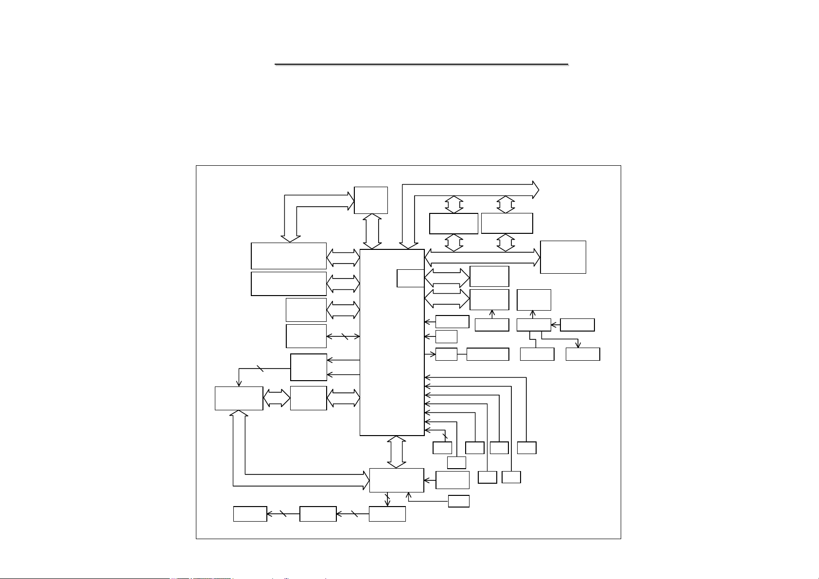
1.3.1 Block Diagram
Mio336i PDA Maintenance
Mio336i PDA Maintenance
Host Address Bus
COM port BUS
Cradle Conn.
NEC color TFT
Module
240*320 / 3.5”
Speaker/0.8W
(Mono)
RS-232 Transceiver (ADM3311)
16550-compatible UART
IrDA/Zilog ZHX1403
Compliant to IrDA 1.1
specification
JTAG CONN.
(For debug use)
EEPROM/24LC00
(Option)
L/R
Back Ligh t
Controller
MP1521
NEC Timing
Controller
Power amplifier
TPA0253
2
LCD bus
Touch Screen bu s
COM1 BUS
IR_TXD
IR_RXD
JTAG
interface
2
PWM
BL_ON/OFF#
LCD control
data bus
USB Client
(Max. 12Mbps)
Intel / PXA255
-300MHz
Audio codec/WM9705
L/R
L/R
Earphone Jack
(Stereo)
SDRAM @ 103MHz
32Mbyte *2
Host Data Bus
SD/MMC
controller
AC’97
interface
SD Control
/data bus
Gauge bus
3.6864M XTAL
32.768K
XTAL
H/W OSC
circuit
5
Joystick
Micro Ph one
Input (m ono)
When earphon e inserted, sp eaker output will be muted.
Home
button
24.576M
XTAL
SD/MMC Socket
Micro control ler
EM78P156
3.6864M XTAL
Red LED
(for Notification)
Contact
button
Intel StrataF lash
28F256L30/K3 *1
Calendar
button
Task
button
Power
button
Li-Ion
Battery
930mAH
Charger
BQ24010
Green LED
(for charger)
Record
button
Extend GPIO
74LCX374
LCD/Panel/Audio
control
DC Adapter-In
(5V)
Amber LED
(for charger)
6
Power Structure
Mio336i PDA Maintenance
Mio336i PDA Maintenance
Battery
(3.5~4.2V)
930mAH
Charger
BQ24010
VCC_P+
(5V)
CPU Core – PXA255
Amplifier – TPA0253
These part can be shut-down
when it’s not active
Can be turned-OFF
when display is OFF
If Adapter plug-in,
The way will be
disconnect ed
MOS
Switch
Can be turned-OFF when
in sleep mode
AAT3110
VCC_5V
VCC_CORE
AMP_5V
VCC_+15
VCC_-15
Turn ON/OFF all
of system power
M/E
Switch
MP1521
(Backlight Controller)
These part can be shut-down
when it’s not active
VCC_IN
VCC_IN
TPS62000
ML4854
VCC_IN
AIC1896
VCC3_LCD
AME8815
VCC_IN
MOS
Switch
MIC5207
VCC1.8VSB
Flash -28F256L30
VCC_3VSB
VCC_3VSB
MOS
Switch
CPU I/O -- PXA255
SDRAM -- K4S561633C
Flash -- 28F256L30/K3
Reset IC -- MIC811
COM Port -- MAX3243
IrDA -- ZHX1403
Micro-P -- EM78P156
EEPROM --24LC00
Extend GPIO --74LCX374
SD Card
MOS
Switch
VCC_AUD
Codec – WM9705
Microphone
LCD Panel
LCD Timing ASIC
VCC3_LCD
7

Mio336i PDA Maintenance
Mio336i PDA Maintenance
1.3.2 Main Board
1.3.2.1 CPU : Intel PXA255, 300MHz
The PXA255 applications processors provide high integration, high performance and low power consumption for
portable handheld and handset devices. These applications processors incorporate Intel’s XScaleTM
Microarchitecture based on the ARM* V5TE architecture. The applications processor’s memory interface supports
a variety of memory types that allow flexibility in design requirements. Hooks for connection to two companion
chips permit glueless connection to external devices. An integrated LCD display controller provides support for
displays, and permits 1, 2 and 4 bit grayscale and 8 or 16 bit color pixels. A 256-byte palette RAM provides
flexibility in color mapping. A rich set of serial devices as well as general system resources provide enough
compute and connectivity capability for many applications. For details on the programming model and theory of
operation of each of these units, refer to the Intel® PXA255 and PXA210 Applications Processors Developer's
Manual.
Product Features
High Performance Processor
- Intel® XScale™ Microarchitecture
- 32 KB Instruction Cache3
- 2 KB Data Cache
- 2 KB “mini” Data Cache
- Extensive Data Buffering
8

Mio336i PDA Maintenance
Mio336i PDA Maintenance
Intel® Media Processing Technology
- Enhanced 16-bit Multiply
- 40-bit Accumulator
Flexible Clocking
- CPU clock from 66 to 300 MHz
- Flexible memory clock ratios
- Frequency change modes
Rich Serial Peripheral Set
- AC97 Audio port
- I2S Audio port
- USB client controller
- High speed UART
- Second UART with flow control
- FIR and SIR infrared comm ports
Low Power
- Less than 500mW typical internal dissipation
- Supply voltage may be reduced to 0.85V
- Low power/Sleep modes
High Performance Memory Controller
- Four Banks of SDRAM – up to 100MHz
- Five Static Chip Selects
- Support for PCMCIA or Compact Flash
- Companion Chip Interface
9

Mio336i PDA Maintenance
Mio336i PDA Maintenance
Additional Peripherals for System Connectivity
- Multimedia card controller (MMC)
- SSP controller
- I²C controller
- Two Pulse Width Modulators (PWMs)
- All peripheral pins double as GPIOs
Hardware Debug Features
Hardware Performance Monitoring Features
10
Mio336i PDA Maintenance
Mio336i PDA Maintenance
Voltage, temperature, and frequency Electrical Specifications
Low Voltage Range (PXA250 and PXA210)
Medium Voltage Range (PXA250 and PXA210)
High Voltage Range (PXA250)
UnitsMaxTypicalMinDescriptionSymbol
ºC85--40Ambient Temperature - Extended TemptA
ºC70-0Ambient Temperature - Nominal TemptA
V0.30-0.3VSS, VSSN, VSSQ VoltageWSS
V3.63.33.0VCCQ VoltageWCCQ
V3.62.5/3.32.375VCCN VoltageWCCN
V0.9350.850.765VCC, PLL_VCC Voltage, Low RangeWCC_L
MHz132.799.5Turbo Mode Frequency, Low RangefTURBO_L
MHz99.550External Synchronous Memory Frequency, Low RangefSDRAM_L
V1.101.000.90VCC, PLL_VCC Voltage, Mid RangeWCC_M
MHz199.199.5Turbo Mode Frequency, Mid RangefTURBO_M
MHz99.550External Synchronous Memory Frequency, Mid RangefSDRAM_M
V1.211.100.99VCC, PLL_VCC Voltage, High RangeWCC_H
Peak Voltage Range (PXA250)
MHz298.799.5Turbo Mode Frequency, High RangefTURBO_H
MHz99.550External Synchronous Memory Frequency, High RangefSDRAM_H
V1.431.301.17VCC, PLL_VCC Voltage, Peak RangeWCC_P
MHz398.299.5Turbo Mode Frequency, Peak RangefTURBO_P
MHz99.550External Synchronous Memory Frequency, Peak RangefSDRAM_P
11
Mio336i PDA Maintenance
Mio336i PDA Maintenance
Note 1: Part number change approved for C1 stepping
PXA250C1 PXA255A0
Note 2: 301-400MHz commercial temperature range is reduced from 0-70C to 0-60C Ta (Ambient Temperature).
Note 3: PXA250 C stepping Core voltage & frequency updated:
Voltage and frequency Specifications
VCC (Volts)Turbo Mode Frequency (MHz)
Max
118.0
199.1
298.7
998.2
MinMin
0.9599.5
0.9599.5
1.04599.5
1.23599.5
Typ
1.0
1.0
1.1
1.3
Max
1.155
1.32
1.43
1.65
Note 1: PXA255 (PXA250 C stepping) ID values updated:
PXA255 ID Values
JTAG IDARM IDStepping
0x692640130x69052D06A0
Package Introduction
The applications processor is offered in the packages: 256-pin mBGA
12

Mio336i PDA Maintenance
Mio336i PDA Maintenance
1.3.2.2 RAM : Synchronous DRAM (SDRAM)
SAMSUNG 256M-bit (16Mx16) Synchronous DARM
Description
The K4S561633C is 268, 435, 456 bits synchronous high data rate Dynamic RAM organized as 4 x 4, 196, 304
words by 16bits, fabricated with SAMSUNG high performance CMOS technology. Synchronous design allows
precise cycle controls with the use of system clock I/O transactions are possible on every clock cycle. Range of
operating frequencies, programmable burst length and programmable latencies allow the same device to be useful
for a variety of high bandwidth, high performance memory system applications.
Feature :
3.0V power supply
LVTTL compatible with multiplexed address
Four banks operation
MRS cycle with address key programs
- CAS latency (1& 2 & 3)
- Burst length (1, 2, 4, 8 & Full page)
- Burst type (Sequential & Interleave)
EMRS cycle with address key programs
All inputs are sampled at the positive going edge of the system clock
DQM for masking
13
Mio336i PDA Maintenance
Mio336i PDA Maintenance
Auto refresh
64ms refresh period (8K cycle)
Commercial Temperature Operation (-25’C ~ 70’C)
Extended Temperature Operation ( -25’C ~ 85’C)
54balls CSP
Package Information :
54Ball (6x9) CSP
219873
VDDDQ0VDDQVSSQDQ15VSSA
DQ1DQ2VSSQVDDQDQ13DQ14B
DQ3DQ4VDDQVSSQDQ11DQ12C
DQ5DQ6VSSQVDDQDQ9DQ10D
DQ7LDQMVDDVSSNCDQ8E
WERASCASCKECLKUDQMF
CSBA1BA0A9A11A12G
A10A1A0A6A7A8H
VDDA2A3A4A5VSSJ
14
Mio336i PDA Maintenance
Mio336i PDA Maintenance
Recommended operation conditions (Voltage reference to VSS=0V, TA=-25C~70C(Commercial),
-25C~85C (Extended))
Note
1
2
IOH=2mA
IOL=2mA
3uA10--10ILIInput leakage current
VDD
VIH
VIL
VOH
VOL
3.6
3.6
0.5
-
0.4
UnitMaxTypSymbol
V
V3.63.02.7VDDQ
V
V
V
V
MinParameter
2.7Supply voltage
3.0
2.2Input logic high voltage
3.0
-0.3Input low voltage
0
2.4Output logic high voltage
-
-Output logic low voltage
-
Note 1: Pin to pin compatible SDRAM vender & part number:
(1) SAMSUNG K4S561633C-RL(N)
(2) INFINEON HYB39L256160AC
(3) MICRON MT48LC16M16LFFG-
15

Mio336i PDA Maintenance
Mio336i PDA Maintenance
1.3.2.3 ROM : 32Mbyte INTEL STRATAFLASH , 28f256K3/L30 (options one)
K3 Performance
- 110/115/120 ns Initial Access Speed for 64/128/256Mbit Densities
- 25 ns Asynchronous Page-Mode Reads, 8 Words Wide
- 13 ns Synchronous Burst-Mode Reads, 8 or 16 Words Wide
- 32-Word Write Buffer
- Buffered Enhanced Factory Programming
K3 Architecture
- Multi-Level Cell Technology: High Density at Low Cost
- Symmetrical 64 K-Word Blocks
- 256Mbit (256 Blocks)
- 128Mbit (128 Blocks)
- 64Mbit (64 Blocks)
- Ideal for “CODE + DATA” applications
K3 Packaging and Voltage
- 64-Ball Intel® Easy BGA Package
- 56-and 79-Ball Intel® VF BGA Package
- VCC = 2.70 V – 3.60 V
- VCCQ = 1.65 – 1.95 V or 2.70 V– 3.60 V
16

Mio336i PDA Maintenance
Mio336i PDA Maintenance
L30 description:
The 1.8 Volt Intel StrataFlash. wireless memory with 3-Volt I/O product is the latest generation of Intel StrataFlash.
memory devices featuring flexible, multiple-partition, dual operation. It provides high performance synchronousburst read mode and asynchronous read mode using 1.8 volt low-voltage, multilevel cell (MLC) technology.
The multiple-partition architecture enables background programming or erasing to occur in one partition while
code execution or data reads take place in another partition. This dual-operation architecture also allows two
processors to interleave code operations while program and erase operations take place in the background.
The 1.8 Volt Intel StrataFlash. wireless memory with 3-Volt I/O device is manufactured using Intel 0.13 ¦Ìm ETOX.
VIII process technology. It is available in industry-standard chip scale packaging.
L30 High performance Read-While-Write/Erase
- 85 ns initial access
- 52MHz with zero wait state, 17 ns clock-to-data output synchronous-burst mode
- 25 ns asynchronous-page mode
- 4-, 8-, 16-, and continuous-word burst mode
- Burst suspend
- Programmable WAIT configuration
- Buffered Enhanced Factory Programming(Buffered EFP): 3.5 µs/byte (Typ)
- 1.8 V low-power buffered and non-buffered programming @ 10 µs/byte (Typ)
L30 Architecture
- Asymmetrically-blocked architecture
- Multiple 8Mbit partitions: 64Mb and 128Mb devices
17

Mio336i PDA Maintenance
Mio336i PDA Maintenance
- Multiple 16Mbit partitions: 256Mb devices
- Four 16KWord parameter blocks: top or bottom configurations
- 64K-Word main blocks
- Dual-operation: Read-While-Write (RWW) or Read-While-Erase (RWE)
- Status register for partition and device status
L30 Power
- 1.7 V - 2.0 V VCC operation
- I/O voltage: 2.2 V - 3.3 V
- Standby current: 30 µA (Typ)
- 4-Word synchronous read current: 17 mA (Typ) @ 54 MHz
L30 Software
- 20 µs (Typ) program suspend
- 20 µs (Typ) erase suspend
- Intel® Flash Data Integrator (FDI) optimized
- Basic Command Set (BCS) and Extended Command Set (ECS) compatible
- Common Flash Interface (CFI) capable
L30 Security
- OTP space:
- 64 unique device identifier bits
- 64 user-programmable OTP bits
- Additional 2048 user-programmable OTP bits
- Absolute write protection: VPP = GND
- Power-transition erase/program lockout
18

Mio336i PDA Maintenance
Mio336i PDA Maintenance
- Individual zero-latency block locking
- Individual block lock-down
L30 Quality and Reliability
- Expanded temperature: –25 C to +85 C
- Minimum 100,000 erase cycles per block
- ETOX™ VIII process technology (0.13 µm)
L30 Density and Packaging
- 64-, 128- and 256Mbit density in VF BGA packages.
- 128/0, and 256/0 Density in Stacked-CSP
- 16-bit wide data bus
19

Mio336i PDA Maintenance
Mio336i PDA Maintenance
1.3.2.4 Audio Codec : WM9705 Multimedia AC’97 Codec with Integrated Touch
Screen Controller
The WM9705 is a high-quality stereo audio codec with an integrated touch screen controller. The audio section is
compliant with the Intel AC’97 Rev 2.2 specification. It performs full-duplex 18 bit codec functions and supports
variable sample rates from 8 to 48k samples/s with high signal to noise ration. Optional AC’97 features include 3D
sound enhancement, line-level outputs, stereo buffered headphone outputs, hardware sample rate version, primary/
secondary mode operation and S/PDIF output. Headphone auto-detect, I²S output and headphone buffer on the
mono output are included. Additionally, the WM9705 integrates a complete 4-wire touch screen controller,
including on-chip screen drivers, pen-down detection feature, and pressure measurement capability.
A 5-pin digital bi-directional AC-Link serial interface allows transfer of control data and DAC and ADC words to
and from the AC’97 controller. The WM9705 is fully operable on 3V or 5V or mixed 3/5V supplies, and is
packaged in the industry standard 48-pin TQFP package with 7mm body size, or in a smaller 7x7x0.9mm QFN.
Features
AC’97 Rev 2.2 compliant codec with pen digitizer
18-bit stereo audio codecs
On-Chip sample rate conversion
Multiple channel input mixer
S/PDIF digital audio output
Headphone drivers on AUX and MONO outputs
20

Mio336i PDA Maintenance
Mio336i PDA Maintenance
Headphone drivers on AUX and MONO outputs
4–wire touch screen interface with co-ordinate and pressure measurement, and pen-down detection
Wake-up from sleep mode on pen down
3V to 5V operation
Extensive power management features including hardware power down option
Standard AC’97 pinout in 48-pin TQFP package or 48-pin QFN package
Recommended operating temperature : -25 ~ 85 ºC (Ta)
21

Mio336i PDA Maintenance
Mio336i PDA Maintenance
1.3.2.5 Audio Amplifier : TI TPA0253
Description
The TPA0253 is a 1-W mono bridge-tied-load (BTL) amplifier designed to drive speakers with as low as 8Ω
impedance. The mono signal is created by summing left and right inputs internally. The amplifier can be
reconfigured on-the-fly to drive two stereo single-ended (SE) signals into head phones. This makes the device ideal
for use in small notebook computers, PDAs, digital personal audio players, anyplace a mono speaker and stereo
head phones are required. From a 5V supply, the TPA0253 can delivery 1W of power into a 8Ω speaker.
The gain of the input stage is set by the user-selected input resistor and a 50kΩ internal feedback resistor (AC=RF/RI). The power stage is internally configured with a gain of –1.25V/V in SE mode, and –2.5V/V in BTL mode.
Thus, the overall gain of the amplifier is 62.5kΩ/RI in SE mode and 125kΩ/RI in BTL mode. The input terminals
are high-impedance CMOS inputs, and can be used as summing nodes. The TPA0253 is available in the 10-pin
thermally-enhanced MSOP package (DGQ) and operates over an ambient temperature range of -40 ºC to 85 ºC .
Features :
Ideal for Notebook Computers, PDA , and Other Small Portable Audio Devices
1 W Into 8 ohm from 5-V Supply
0.3 W Into 8 ohm from 3-V Supply
Stereo Head Phone Drive
Mono (BTL) Signal Created by Summing Left and Right Signals Internally
22

Mio336i PDA Maintenance
Mio336i PDA Maintenance
Wide Power Supply Compatibility 2.5 V to 5.5 V
Low Supply Current
3.2 mA Typical at 5 V
2.7 mA Typical at 3 V
Shutdown Control . . . 1 uA Typical
Shutdown Pin is TTL Compatible
–40C to 85C Operating Temperature Range
Space-Saving, Thermally-Enhanced MSOP Packaging
23
Mio336i PDA Maintenance
Mio336i PDA Maintenance
1.3.2.6 ZILOG : Infrared Component (ZHX1403)
Features :
Compliant to IrDA Data Specification 1.4 Standard Power SIR
Low-power supply voltage range: 2.4 to 3.6 V
ZHX1403 listening current: only 6 A (typically) at 3.0 V (ZiLOG exclusive)
UltraSlim package: 7.3 mm long x 2.8 mm wide x 1.9 mm high
Extended operating temperature range: –30 ºC to +85 ºC
Internal current source eliminates need for a current-limiting resistor for IR LED
Meets IEC 825-1 Class 1 eye safety specifications
Block Diagram
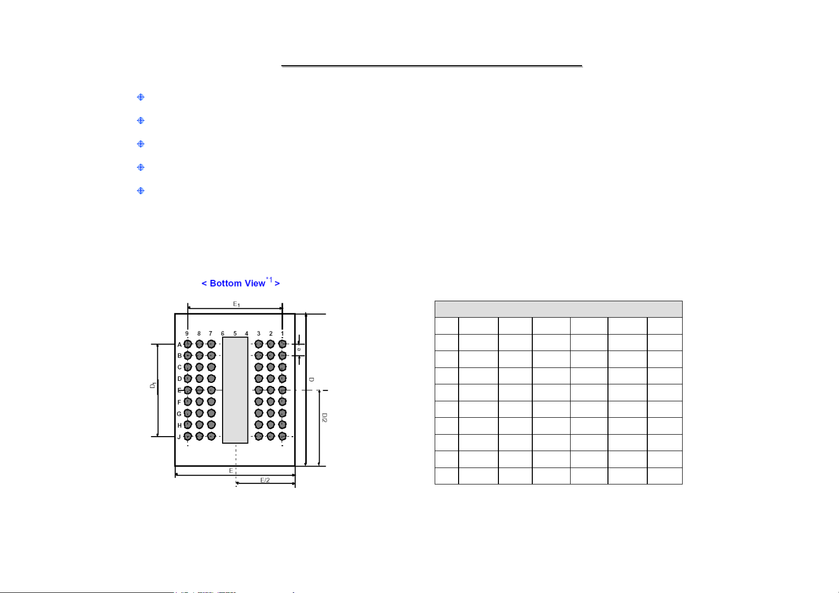
Pin
Name
1
NC
2
VCC
3
GND
4
SD
Test criteria:
Transmission distance : 1 m
Transmission angle : 15
Function
NC (future use)
Supply voltage
Ground
Shutdown
I/O
-
-
-
I
Pin
5
6
7
-
Name
RXD
TXD
LEDA
TAB
Function
Receiver output
Transmitter input
IRED anode
Shield connection
I/O
O
I
-
-
24

Mio336i PDA Maintenance
Mio336i PDA Maintenance
1.3.2.7 UART Transceiver : SIPEX SP3243E
Description
The SP3223E and 3243E products are RS-232 transceiver solutions intended for portable of hand-held applications
such as notebook and palmtop computers. The SP3223E and 3243E use an internal high-efficiency, charge-pump
power supply that requires only 0.1mF capacitors in 3.3V operation. This charge pump and Sipex’s driver
architecture allow the SP3223E/3243E series to deliver compliant RS-232 performance from a single power supply
ranging from +3.3V to +5.0V. The SP3223E is a 2-driver/2-receiver, and the SP3243E is a 3-driver/5-receiver
device ideal for laptop/notebook computer and PDA applications.
The SP3243E includes one complementary receiver that remains alert to monitor an external device’s Ring Indicate
signal while the device is shutdown. The Auto-Online feature allows the device to automatically “wake-up” during
a shutdown state when an RS-232 cable is connected and a connected peripheral is turned on. Otherwise, the device
automatically shuts itself down drawing less than 1mA.
Features :
Meets true EIA/TIA-232-F standards from a +3.0V to +5.5V power supply
Interoperable with EIA/TIA-232 and adheres to EIA/TIA-562 down to a +2.7V power source
Auto-Online circuitry automatically wakes up from a 1mA shutdown
Minimum 120Kbps data rate under load
Regulated charge pump yields stable RS-232 outputs regardless of Vcc variations
25

Mio336i PDA Maintenance
Mio336i PDA Maintenance
Enhanced ESD specifications :
- +15KV human body model
- +15KV IEC1000-4-2 air discharge
- +8KV IEC1000-4-2 contact discharge
Power Dissipation :
28-pin SSOP (derate 11.2mW/ºC above +70 ºC ) … 900mW
Operation temp. : 0 ºC to +70 ºC
26

Mio336i PDA Maintenance
Mio336i PDA Maintenance
1.3.2.8 LCD Timing Controller : NL2432DR22 (For NEC Panel)
Features:
Operating Temperature Range: -25~75°C
Supply Voltage Range: 2.5~3.6V
Power Consumption:
10mW(DCK=6.36MHz.VDD=3.3V)
Package:
Package: Type - TQFP
Number of Pin - 80 pins
Size (L x W x T) – 12.1mm x 12.1mm x 1.1mm
27
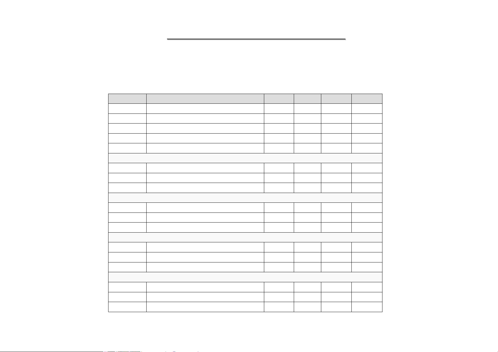
Pin outline :
Mio336i PDA Maintenance
Mio336i PDA Maintenance
In/Out putSymbolsPin
PVDD1
IBI52
IBI43
IBI34
IBI25
IBI16
I/O Buffer
-
IBC
IBC
IBC
IBC
IBC Input Data Blue Bit1
Output Current
-
-
-
-
-
-
Capacity
-
-
-
-
-
-
Frequency
7.5MHz
7.5MHz
7.5MHz
7.5MHz
7.5MHz
Supply Voltage (2.3V to 3.6V)
Input Data Blue Bit5
Input Data Blue Bit4
Input Data Blue Bit3
Input Data Blue Bit2
GND Terminal----PGND7
Input Data Blue Bit07.5MHz--IBCIBI08
Input Data Green Bit57.5MHz--IBCIGI59
Input Data Green Bit47.5MHz--IBCIGI410
Input Data Green Bit37.5MHz--IBCIGI311
Input Data Green Bit37.5MHz--IBCIGI312
Input Data Green Bit27.5MHz--IBCIGI213
Input Data Green Bit17.5MHz--IBCIGI114
Supply Data (2.3V to 3.6V)----PVDD14
Mark
Input Data Green Bit07.5MHz--IBCIGI015
Input Data Red Bit57.5MHz--IBCIRI516
Input Data Red Bit47.5MHz--IBCIRI417
Input Data Red Bit37.5MHz--IBCIRI318
Input Data Red Bit27.5MHz--IBCIRI219
GND Terminal----PGND20
28
Mio336i PDA Maintenance
Mio336i PDA Maintenance
In/Out putSymbolsPin
PVDD21
IRI122
IRI023
PGND24
IDCK25
PGND26
I/O Buffer
-
IBC
IBC
-
IBC
- GND Terminal
Output Current
-
-
-
-
-
-
Capacity
-
-
-
-
-
-
Frequency
-
7.5MHz
7.5MHz
-
15MHz
-
Supply Voltage (2.3V to 3.6V)
Input Data Red Bit1
Input Data Red Bit0
GND Terminal
Dot Clock
Data Enable Signal18.75MHz--IBCIDE27
TEST Terminal (0: Normal, 1: Test Mode)DC---PTSTEN228
Gate-Driver Output Enable TerminalDC--IBCD1IOEN29
Power On Clear (0: reset, 1: reset off)---IBHIPOC30
Supply Voltage (2.3V to 3.6V)----PVDD31
Polarity Change18.75KHz40pF2mAOB1TOPC32
Source-Driver Output Enable Signal18.75MHz40pF2mAOB1TOHOE33
Output Data Inversion Signal7.5MHz40pF2mAOB1TOINV34
H-Driver Latch Pulse18.75MHz40pF2mAOB1TODLP35
Mark
H-Driver Inhibit Pulse9.375MHz40pF2mAOB1TOINH36
H-Driver Start Pulse18.75MHz40pF2mAOB1TOHSP37
GND Terminal----PGND38
H-Driver Clock15MHz40pF6mAOB2TOHCK39
GND Terminal----PGND40
Supply Voltage (2.3V to 3.6V)----PVDD41
Output Data Blue Bit07.5MHz40pF2mAOB1TOBO042
Output Data Blue Bit17.5MHz40pF2mAOB1TOBO143
29
 Loading...