

Page 1
SERVICE MANUAL FOR
SERVICE MANUAL FOR
SERVICE MANUAL FOR
8355
8355
83558355
8355
8355
83558355
8355
8355
83558355
BY:
Repair Technology Research Department /EDVD
Repair Technology Research Department /EDVD
Nov.2003
Rain Li
Rain Li
Page 2

Contents
8355 N/B MAINTENANCE
8355 N/B MAINTENANCE
1. Hardware Engineering Specification …………………………………………………………………
1.1 Introduction ………………………………………………………………………………………………………….
1.2 System Hardware Part……………………………………………………………………………………………….
1.3 Other Functions ………………………………………………………………………………………………………
1.4 Peripheral Components………………………………………………………………………………………………
1.5 Power Management…………………………………………………………………………………………………..
1.6 Appendix 1 : VT8235 GPIO Definition……………………………………………………………………………...
1.7 Appendix 2 : H8 Pins Definition …………………………………………………………………………………….
1.8 Appendix 3 : 8355 Product Specification ……………………………………………………………………………
2. System View and Disassembly ………………………………………………………………………...
2.1 System View …………………………………………………………………………………………………………
2.2 System Disassembly …………………………………………………………………………………………………
3. Definition & Location of Connectors / Switches ……………………………………………………..
3.1 Mother Board ………………………………………………………………………………………………………..
4
4
6
47
52
53
56
58
63
66
66
69
95
95
4. Definition & Location of Major Components ………………………………………………………..
4.1 Mother Board ………………………………………………………………………………………………………..
5. Pin Description of Major Component …….………………………………………………………….
5.1 AMD AthlonTM64 Processor ……………………………………………………………………………………….
5.2 K8T800M (VT8385) North Bridge …………………………………………………………………………………
98
98
100
100
102
1
Page 3

Contents
8355 N/B MAINTENANCE
8355 N/B MAINTENANCE
5.3 VT8235 South Bridge ……………………………………………………………………………………………….
6. System Block Diagram ………………………………………………………………………………..
7. Maintenance Diagnostics ………………………………………………………………………………
7.1 Introduction …………………………………………………………………………………………………………
7.2 Error Codes …………………………………………………………………………………………………………
7.3 Debug Tool …………………………………………………………………………………………………………..
8. Trouble Shooting ………………………………………………………………………………………
8.1 No Power …………………………………………………………………………………………………………….
8.2 Battery Can not Be Changed ………………………………………………………………………………………
8.3 No Display ……………………………………………………………………………………………………………
8.4 AGP Controller Failure LCD No Display …………………………………………………………………………
8.5 External Monitor No Display ………………………………………………………………………………………
8.6 Memory Test Error …………………………………………………………………………………………………
8.7 Keyboard (K/B) Touch-Pad (T/P) Test Error ……………………………………………………………………..
8.8 Hard Driver Test Error ……………………………………………………………………………………………..
8.9 CD-ROM Driver Test Error…………………………………………………………………………………………
8.10 USB Port Test Error ………………………………………………………………………………………………..
8.11 PC Card Socket Failure ……………………………………………………………………………………………
8.12 Memory-Card Socket Failure ……………………………………………………………………………………..
8.13 IEEE1394 Test Error……………………………………………………………………………………………….
8.14 LAN Test Error……………………………………………………………………………………………………..
106
115
116
116
117
119
121
122
126
128
132
132
136
138
140
142
144
147
149
151
153
2
Page 4

Contents
8355 N/B MAINTENANCE
8355 N/B MAINTENANCE
8.13 Audio Failure ………….……………………………………………………………………………………………
9. Spare Parts List ………………………………………………………………………………………..
10. System Exploded Views ………………………………………………………………………………
11. Circuit Diagram ………………………………………………………………………………………
12. Reference Material …………………………………………………………………………………...
155
158
172
174
207
3
Page 5

8355 N/B MAINTENANCE
8355 N/B MAINTENANCE
1. Hardware Engineering Specification
1.1 Introduction
The 8355 motherboard would support the AMD ClawHammer K8 processor with uPGA Package,
2700+/3000+/3300+/3600+/3900+/4200+, FSB 800MHz
This system is based on PCI architecture, which have standard hardware peripheral interface. The power management
complies with Advanced Configuration and Power Interface (ACPI) 2.0. It also provides easy configuration through
CMOS setup, which is built in system BIOS software and can be pop-up by pressing F2 at system start up or warm
reset. System also provides ico LEDs to display system status, such as AC Power, Battery Power, Battery status, CD-
ROM, HDD, NUM LOCK, CAP LOCK, SCROLL LOCK, WIRELESS LAN status. It also equipped 4 USB2.0 ports.
The memory subsystem supports 0MB on board; Expandable up to 1024MB Expandable with combination of optional
128/256/512 MB memory 200-pin DDR 266/333/400 Memory Module x2, PC-2100/2700/3200 specification
The K8T800 North Bridge plus VT8235 South Bridge chipset is a high performance, cost-effective and energy
efficient solution for the implementation of desktop personal computer systems with 8 / 16-bit 800 / 600 / 400 / 200
MHz HyperTransport. CPU host interface based on AMD K8 / ClawHammer. processors.
The VT8235 “V-Link Client Controller” is a highly integrated PCI /LPC controller. Its internal bus structure is based
on a 66 MHz PCI bus that provides 2x bandwidth compared to previous generation PCI bridge chips. The VT8235
also provides a 533 MB/sec bandwidth Host / Client V-Link interface with V-Link-PCI and V-Link-LPC controllers.
It supports six PCI slots of arbitration and decoding for all integrated functions and LPC bus.
4
Page 6

8355 N/B MAINTENANCE
8355 N/B MAINTENANCE
The RADEON MOBILITY 9600 provides the fastest and most advanced 2D, 3D, and multimedia graphics
performance for the latest applications in full 32-bit color. Its architecture introduces the latest achievements in the
graphics industry, which enable the use of the progressive new features in upcoming applications, but without
compromising performance. ATI’s exclusive support of DirectX® 9.0 features, highly optimized OpenGL® support,
and flexible memory configurations allow implementations targeted at both gaming enthusiast and workstation
platforms.
To provide for the increasing number of multimedia applications, the AC97 CODEC CMI9738-S is integrated onto
the motherboard
A full set of software drivers and utilities are available to allow advanced operating systems such as Windows XP and
Windows 2000 to take full advantage of the hardware capabilities such as bus mastering IDE, Windows 95-ready Plug
& Play, Advanced Power Management (APM) and Advance configuration and power interface (ACPI).
Following chapters will have more detail description for each individual sub-systems and functions.
5
Page 7
8355 N/B MAINTENANCE
8355 N/B MAINTENANCE
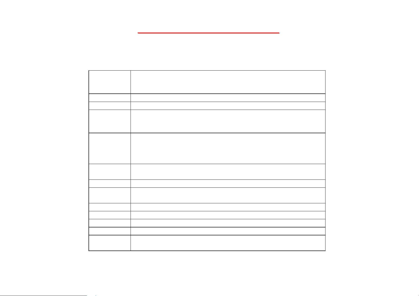
1.2 System Hardware Part
CPU AMD ClawHammer K8 processor with uPGA Package
2700+/3000+/3300+/3600+/3900+/4200+
FSB 800MHz
Core logic VIA K8T800 + VT8235
VGA Control ATI M10P with 64MB External VRAM (Reserve for 128MB VRAM)
System BIOS Insyde 256 KB Flash EPROM (Include System BIOS and VGA BIOS)
ACPI 2.0; DMI 2.3.1 compliant
Plug & Play capability
Memory 0MB on board; Expandable up to 1024MB
Expandable with combination of optional 128/256/512 MB memory
200-pin DDR 266/333/400 DRAM Memory Module x2,
PC-2100/2700/3200 specification
Clock
Generator
IEEE1394 VT6307L
Audio System AC97 CODEC: C-MEDIA ELECTRONICS INC., CMI9738-S
Super I/O PC87397
Modem 56Kbps(V.90, worldwide) MDC Modem
PHY of LAN VT6103 10/100 base -T PHY
PCMCIA ENE710
CARD
READER
ICS 950403
Power Amplifier: Anpec APA2020
ENE710
6
Page 8

8355 N/B MAINTENANCE
8355 N/B MAINTENANCE
1.2.1 CPU_ ClawHammer PROCESSOR
The ClawHammer processor family is designed to support performance desktop and workstation applications. It
provides a high-performance HyperTransport. link to I/O, as well as a single 64-bit high-performance DDR
memory controller.
Compatible with Existing 32-bit Code Base
Including support for SSE, SSE2, MMX
Runs existing operating systems and drivers
Local APIC on-chip
AMD x86-64 Technology
AMD.s 64-bit x86 instruction set extensions
64-bit integer registers, 48-bit virtual addresses, 40-bit physical addresses
Eight new 64-bit integer registers (16 total)
Eight new 128-bit SSE/SSE2 registers (16 total)
Integrated Memory Controller
Low-latency, high-bandwidth
72-bit DDR at 200, 266, 333, and 400 MHz (64-bits + 8-bits ECC)
TM
, 3DNow!TM, technology and all legacy x86 instructions
7
Page 9

8355 N/B MAINTENANCE
8355 N/B MAINTENANCE
HyperTransport. Technology to I/O Devices
Two 8-bit links each support 1600 mega-transfers (MT) per second or 1.6 Gbytes/s in each direction
Can be configured as single 16-bit link supporting 1600 MT/s or 3.2 Gbytes/s in each direction
64-Kbyte 2-way Associative ECC-Protected L1 Data Cache
Two 64-bit operations per cycle, 3-cycle latency
64-Kbyte 2-way Associative Parity-Protected L1 Instruction Cache
With advanced branch prediction
16-way Associative ECC-Protected L2 Cache
Exclusive cache architecture.storage in addition to L1 caches
256 KB, 512 KB, and 1 MB options
Machine Check Architecture
Includes hardware scrubbing of major ECC-protected arrays
Power Management
Multiple low-power states
System Management Mode (SMM)
8
Page 10

8355 N/B MAINTENANCE
8355 N/B MAINTENANCE
ACPI 2.0 compliant, including support for processor performance states
Power Supplies
VDD (core): 1.50-V at 52 Amps (max)
VDDIO: 2.5-V at 3.0 Amps (max) for DDR I/O
VLDT: 1.2-V at 0.5 Amps for HyperTransport
VTT: 1.25-V at 0.5 Amps required for 2.5-V I/Os
Target CPU Core Power: 78.00 Watts
Target Maximum Thermal Power: 89 Watts
Electrical Interfaces
HyperTransport. Technology: LVDS-like differential, unidirectional
DDR: SSTL per JEDEC DDR specification
Clock, reset, and test signals also use DDR-like electrical specifications
Packaging
754-pin lidded micro PGA
1.27-mm pin pitch
29x29 row pin array
40mm x 40mm organic substrate, Organic C4 die attach
9
Page 11

8355 N/B MAINTENANCE
8355 N/B MAINTENANCE
1.2.2 System frequency
1.2.2.1 System frequency synthesizer_ICS950402
Programmable Timing Control Hub™ AMD-K8™ processor
General Description
The ICS950403 is a main system clock solution for desktop designs using the AMD K8 CPU. It provides all
necessary clock signals for Clawhammer and Sledgehammer systems.
The ICS950403 is part of a whole new line of ICS clock generators and buffers called TCH™ (Timing Control
Hub). This part incorporates ICS's newest clock technology which offers more robust features and functionality.
Employing the use of a serially programmable I2C interface, this device can adjust the output clocks by configuring
the frequency setting, the output divider ratios, selecting the ideal spread percentage, the output skew, the output
strength, and enabling/disabling each individual output clock. M/N control can configure output frequency with
resolution up to 0.1MHz increment.
Recommended Application:
AMD K8 System Clock with AMD or VIA Chipset
Output Features:
2 - Differential pair push-pull K8 CPU clocks
9 - PCICLK (Including 1 free running) @3.3V
3 - Selectable PCICLK/HTTCLK @3.3V
1 - HTTCLK @3.3V
10
Page 12

8355 N/B MAINTENANCE
8355 N/B MAINTENANCE
1 - 48MHz, @3.3V fixed.
1 - 24/48MHz @ 3.3V
3 - REF @3.3V, 14.318MHz.
Features:
Programmable output frequency.
Programmable output divider ratios.
Programmable output rise/fall time.
Programmable output skew..
Programmable spread percentage for EMI control.
Watchdog timer technology to reset system if system malfunctions.
Programmable watch dog safe frequency.
Support I2C Index read/write and block read/write operations.
Uses external 14.318MHz crystal.
Supports Hyper Transport Technology (HTTCLK).
11
Page 13

8355 N/B MAINTENANCE
8355 N/B MAINTENANCE
1.2.3 VIA K8T800+VT8235
1.2.3.1 K8T800
The K8T800 is a high performance, cost-effective and energy efficient solution for the implementation of desktop
personal computer systems with 8 / 16-bit 800 / 600 / 400 / 200 MHz HyperTransport. CPU host interface based on
AMD K8 / ClawHammer. processors.
Defines Highly Integrated Solutions for Performance PC Desktop Designs
High performance North Bridge with HyperTransport. interface to AMD. K8 CPU plus AGP 8x external bus to
external Graphics Controller plus high-speed V-Link interface to chipset South Bridge
Combines with VIA K8T400M V-Link South Bridge for integrated LAN, Audio, ATA133 IDE, and 6 USB 2.0
ports
578 Ball Grid Array package with 35 x 35 mm body size, 1.27mm ball pitch, and heat spreader
2.5V core, 0.22 u process
High Performance K8 CPU Interface
Chipset support for AMD. K8 / ClawHammer. processor
Processor interface via HyperTransport. bus
Separate transmit and receive buses for no lost bus turnaround cycles
All transmit and receive signals use 2 pin low-voltage-swing differential signalling for high-reliability and high
speed
12
Page 14

8355 N/B MAINTENANCE
8355 N/B MAINTENANCE
8 or 16-bit control / address / data transfer both directions
800 / 600 / 400 / 200 MHz Double Data Rate operation both directions
Default 8-bit / 200 MHz operation on startup for high reliability with speedup to dual 16-bit, 800 MHz operation (3.2
GB/sec total bandwidth) under software control (transmit and receive may be different widths and / or speeds)
Full Featured Accelerated Graphics Port (AGP) 8x Controller
Supports 533 MHz 8x, 266 MHz 4x, and 133 MHz 2x transfer modes for AD and SBA signaling
AGP v3.0 compliant with 8x transfer mode
Pseudo-synchronous with the host CPU bus with optimal skew control
Supports SideBand Addressing (SBA) mode (non-multiplexed address / data)
AGP pipelined split-transaction long-burst transfers up to 1GB/sec
Eight level read request queue
Four level posted-write request queue
Thirty-two level (quadwords) read data FIFO (256 bytes)
Sixteen level (quadwords) write data FIFO (128 bytes)
Intelligent request reordering for maximum AGP bus utilization
Supports Flush/Fence commands
Graphics Address Relocation Table (GART)
One level TLB structure
Sixteen entry fully associative page table
13
Page 15

8355 N/B MAINTENANCE
8355 N/B MAINTENANCE
LRU replacement scheme
Independent GART lookup control for host / AGP / PCI master accesses
Windows 95 OSR-2 VXD and integrated Windows 98 / 2000 / XP miniport driver support
High Bandwidth 533 MB / Sec 8-bit V-Link Host Controller South Bridge Interface
Supports 66 MHz V-Link Host interface with total bandwidth of 533 MB/sec
Operates in 2x, 4x, and 8x modes
Full duplex commands with separate command / strobe
Request / Data split transaction
Configurable outstanding transaction queue for Host to V-Link Client accesses
Supports Defer / Defer-Reply transactions
Transaction assurance for V-Link Host to Client access eliminates V-Link Host-Client Retry cycles
Intelligent V-Link transaction protocol to eliminate data wait-state / throttle transfer latency
All V-Link transactions for both Host and Client have a consistent view of transaction data depth and buffer size to
avoid data overflow
Highly efficient V-Link arbitration with minimum overhead
All V-Link transactions have predictable cycle length with known command / data duration
14
Page 16

8355 N/B MAINTENANCE
8355 N/B MAINTENANCE
1.2.3.2 VT8235
The VT8235 South Bridge is a high integration, high performance, power-efficient, and high compatibility device
that supports Intel and non-Intel based processor to V-Link bus bridge functionality to make a complete Microsoft
PC2001-compliant PCI/LPC system. The VT8235 includes standard intelligent peripheral controllers:
a) IEEE 802.3 compliant 10 / 100 Mbps PCI bus master Ethernet MAC with standard MII interface to external
PHYceiver.
b) Master mode enhanced IDE controller with dual channel DMA engine and interlaced dual channel commands.
Dedicated FIFO coupled with scatter and gather master mode operation allows high performance transfers between
PCI and IDE devices. In addition to standard PIO and DMA mode operation, the VT8235 also supports the
UltraDMA-133, 100, 66, and 33 standards to allow reliable data transfer at rates up to 133 MB/sec. The IDE
controller is SFF-8038i v1.0 and Microsoft Windows-family compliant.
c) Universal Serial Bus controller that is USB v2.0 / 1.1 and Universal HCI v2.0 / 1.1 compliant. The VT8235
includes three root hubs with six function ports with integrated physical layer transceivers. The USB controller
allows hot plug and play and isochronous peripherals to be inserted into the system with universal driver support.
The controller also implements legacy keyboard and mouse support so that legacy software can run transparently in
a non-USB-aware operating system environment.
d) Keyboard controller with PS2 mouse support.
e) Real Time Clock with 256 byte extended CMOS. In addition to the standard ISA RTC functionality, the
integrated RTC also includes the date alarm, century field, and other enhancements for compatibility with the ACPI
standard.
15
Page 17

8355 N/B MAINTENANCE
8355 N/B MAINTENANCE
f) Notebook-class power management functionality compliant with ACPI and legacy APM requirements. Multiple
sleep states (power-on suspend, suspend-to-DRAM, and suspend-to-Disk) are supported with hardware automatic
wake-up. Additional functionality includes event monitoring, CPU clock throttling and stop (Intel processor
protocol), PCI bus clock stop control, modular power, clock and leakage control, hardware-based and software-
based event handling, general purpose I/O, chip select and external SMI.
g) Full System Management Bus (SMBus) interface.
h) Integrated bus-mastering dual full-duplex direct-sound AC97-link-compatible sound system.
i) Plug and Play controller that allows complete steerability of all PCI interrupts and internal interrupts / DMA
channels to any interrupt channel. One additional steerable interrupt channel is provided to allow plug and play and
reconfigurability of onboard peripherals for Windows family compliance. The VT8235 also enhances the
functionality of the standard ISA peripherals. The integrated interrupt controller supports both edge and level
triggered interrupts channel by channel. The integrated DMA controller supports type F DMA in addition to
standard ISA DMA modes. Compliant with the PCI-2.2 specification, the VT8235 supports delayed transactions
and remote power management so that slower ISA peripherals do not block the traffic of the PCI bus. Special
circuitry is built in to allow concurrent operation without causing dead lock even in a PCI-to-PCI bridge
environment. The chip also includes eight levels (doublewords) of line buffers from the PCI bus to the ISA bus to
further enhance overall system performance.
16
Page 18

8355 N/B MAINTENANCE
8355 N/B MAINTENANCE
1.2.4 RADEON MOBILITY 9600
General Description
The RADEON MOBILITY 9600 provides the fastest and most advanced 2D, 3D, and multimedia graphics
performance for the latest applications in full 32-bit color. Its architecture introduces the latest achievements in the
graphics industry, which enable the use of the progressive new features in upcoming applications, but without
compromising performance. ATI’s exclusive support of DirectX® 9.0 features, highly optimized OpenGL® support,
and flexible memory configurations allow implementations targeted at both gaming enthusiast and workstation
platforms.
SMARTSHADER™ — Advanced Shader Technology
Provides complete hardware-accelerated support for the new DirectX® 9.0 programmable shader model,
enabling more complex and realistic texture and lighting effects than ever before.
Significant improvement over first-generation shaders introduced in DirectX® 9.0, with a much more powerful
and intuitive instruction set.
Offers full support for this feature in OpenGL® applications.
SMOOTHVISION™ — Flexible Anti-Aliasing and Anisotropic Filtering
The most flexible and efficient anti-aliasing implementation available to date.
Eliminates “jaggies” on the edges of objects, shimmering pixels on distant surfaces, and other visual artifacts for
smoother-looking images.
Offers full support for this feature in OpenGL® applications.
17
Page 19

8355 N/B MAINTENANCE
8355 N/B MAINTENANCE
SMOOTHVISION™ — Flexible Anti-Aliasing and Anisotropic Filtering
The most flexible and efficient anti-aliasing implementation available to date.
Eliminates “jaggies” on the edges of objects, shimmering pixels on distant surfaces, and other visual artifacts
for smoother-looking images.
Unique adaptive process can independently select the anti-aliasing pattern for each pixel within a 4x4 region,
rather than relying on a fixed pattern for the whole image.
Better visual quality with minimal performance degradation.
Supports DirectX® 9.0 multisampling and related effects, including motion blur and depth-of-field.
High Performance Memory Support
Incorporates support for DDR SDRAM/SGRAM at up to 350 MHz.
Features ATI’s second generation HYPER Z™III technology that conserves memory bandwidth for improved
performance in demanding applications.
Boosts effective memory bandwidth by over 20%.
Dual Display Support
Leading-edge technology, fully optimized with HYDRA VISION™, flexibly supports multiple combinations of
traditional CRT monitors, flat panel displays and TV.
Features Dual Channel DVI support.
32-bit PCI bus (Rev 2.2), 3.3 V with bus mastering support.
18
Page 20

8355 N/B MAINTENANCE
8355 N/B MAINTENANCE
Comprehensive AGP support including 1.5 Volt (AGP 4X) and 0.8 Volt (AGP8X) mode operation, sideband
addressing, AGP texturing (direct memory execution), and support for AGP reads and writes, including fast write
capability.
Single channel 128/64-bit memory interface using SGRAM or SDRAM to build 8/16/32/64 MB configurations.
Operating frequency is 67MHz minimum to 350MHz maximum, SDR or DDR.
16-bit Zoom Video port.
Support for ROM or Flash RAM parallel or serial video BIOS.
Two independent CRT controllers to support two asynchronous simultaneous display paths.
Integrated DAC for CRT with stereoscopic display support.
Integrated second DAC for the second CRT (TV) support.
Integrated LVDS interface: single and dual pixel per clock, up to 85MHz per channel.
LCD panel detection.
Integrated TMDS transmitter running up to 165MHz (when matched with coherently clocked receiver; otherwise,
135MHz) for support up to 1600x1200 at 60Hz. Fully compliant with DVI and DFP connection standards.
Radiometric expansion.
Ideal for Windows 2000 and Windows XP
RADEON MOBILITY 9600 provides comprehensive support for all new Windows 2000 and Windows XP
display-oriented features, including acceleration of new GDI extensions like Alpha BLTs, Transparent BLTs,
and Gradient Fills, as well as exclusive, patent-pending hardware alpha cursor support.
19
Page 21

8355 N/B MAINTENANCE
8355 N/B MAINTENANCE
1.2.4.1 General and Interfacing Features
32-bit PCI bus (Rev 2.2), 3.3 V with bus mastering support.
Comprehensive AGP support including 1.5 Volt (AGP 4X) and 0.8 Volt (AGP8X) mode operation, sideband
addressing, AGP texturing (direct memory execution), and support for AGP reads and writes, including fast
write capability.
Single channel 128/64-bit memory interface using SGRAM or SDRAM to build 8/16/32/64 MB configurations.
Operating frequency is 67MHz minimum to 350MHz maximum, SDR or DDR.
16-bit Zoom Video port.
Support for ROM or Flash RAM parallel or serial video BIOS.
Two independent CRT controllers to support two asynchronous simultaneous display paths.
Integrated DAC for CRT with stereoscopic display support.
Integrated second DAC for the second CRT (TV) support.
Integrated LVDS interface: single and dual pixel per clock, up to 85MHz per channel.
LCD panel detection.
Integrated TMDS transmitter running up to 165MHz (when matched with coherently clocked receiver;
otherwise, 135MHz) for support up to 1600x1200 at 60Hz. Fully compliant with DVI and DFP connection
standards. Ratiometric expansion.
Support for external TMDS transmitter via 24-bit digital output to drive most popular TMDS transmitters up to
165MHz frequency.
Internal and external Spread Spectrum support.
Integrated enhanced TV encoder with 10-bit DAC (shared between second CRT DAC and TV).
20
Page 22

8355 N/B MAINTENANCE
8355 N/B MAINTENANCE
Independent DDC lines for DAC and TMDS connections. Also full AppleSense support on DAC connection.
Static and dynamic Power Management support (APM as well as ACPI) with full VESA DPMS and Energy
Star compliance.
PCI bus power management 1.1 and AGP Busy and Stop signals Rev 1.61 and Solano 2-M.
Full POWERPLAYTM and POWER ON DEMAND support.
Comprehensive testability including full internal scan, memory BIST, I/O XOR tree and Iddq. Ideal accelerator
for Windows 2000 and Windows XP - includes patent pending hardware support for the Windows 2000 and
Windows XP alpha cursor, as well as acceleration of new GDI extensions such as Alpha BLTs, Transparent
BLTs, and Gradient Fills.
Fully compliant with PC 2001 requirements.
Fully compliant with Mobile PCI rev 1.0.
Full ACPI 1.0b, OnNow, and IAPC (Instantly Available PC) power management, including PCI power
management registers.
Bi-endian support for compliance on a variety of processor platforms.
Unique enhanced TCA (Triple-Cache Architecture) incorporates texture, pixel and vertex caches to maximize
effective memory bandwidth.
CCE high-speed pull architecture software interface optimized for Pentium III/4 and Athlon systems:
• Bus mastering of 2D&3D display lists.
• Direct walk of Direct3D/OpenGL vertex list.
• Ultra-thin driver layer.
• Maximizes concurrency between RADEON MOBILITY 9000 and host.
Triple 10-bit palette DAC supports pixel rates to 400MHz.
21
Page 23

8355 N/B MAINTENANCE
8355 N/B MAINTENANCE
DDC1 and DDC2ci for plug and play monitors.
Hydravision for dual monitor support.
Hardware I2C.
Integrated hardware diagnostic tests performed automatically upon initialization.
High quality components through at-speed testing, built-in Scan, Iddq, CRC, chip diagnostics, and XOR tree.
Single chip solution in 0.15 micron, 1.2V-1.5V CMOS technology in 696 BGA and 648 BGA package.
Flexible memory support:
• SGRAM or SDRAM.
• SDR or DDR.
• DDR support for both system memory SDRAM and graphics SGRAM devices.
• 128-bit or 64-bit interface.
• 8MB to 64MB.
Comprehensive HDKs, SDKs and utilities augmented by full engineering support.
Complete local language support (contact ATI for current list).
Dual RGB CRT output with DDC.
Integrated enhanced TV encoder based on Rage Theater support at 1024x768.
HDCP 1.0 support on integrated TMDS transmitter.
Digital interface with external TMDS Tx with dedicated DDC, configurable as a 24 bit SDR bus or a 12 bit DDR bus.
Independent h/w icon & h/w cursor on both display paths (simultaneous h/w cursor & icon).
IEEE 1149.1 Scan path interface.
VIP 2.0 with multi channel DMA transfer. Support for Rage Theater via VIP.
22
Page 24

8355 N/B MAINTENANCE
8355 N/B MAINTENANCE
1.2.5 AC’97 AUDIO SYSTEM: C-MEDIA ELECTRONICS INC., CMI9738-S
The CMI9738-S is an 18-bit, full duplex AC'97 2.2 compatible stereo audio CODEC designed for PC multimedia
systems,including host/soft audio and AMR/CNR based designs. The CMI9738-S incorporates proprietary converter
technology to achieve a high SNR, greater than 90 dB. The CMI9738-S AC'97 CODEC supports multiple CODEC
extensions with independent variable sampling rates and built-in 3D effects. The CMI9738-S CODEC provides two
pairs of stereo outputs with independent volume controls, a mono output, and multiple stereo and mono inputs, along
with flexible mixing, gain and mute functions to provide a complete integrated audio solution for PCs.
Features
Single chip audio CODEC with high S/N ratio (>90dB)
Compliant with AC’97 2.2 & WHQL specifications
Support of S/PDIF out is compliant with AC’97 rev2.2 specifications
Meets performance requirements for audio on PC2001 systems
Meets Microsoft PC99 & WLP 2.0 audio requirements
18-bit Stereo full-duplex CODEC with independent and variable sampling rate
18-bit ADC and 20-bit DAC resolution
Four analog line-level stereo inputs with 5-bit volume control: LINE_IN, CD, VIDEO, AUX
High quality differential CD input
Two analog line-level mono input: PC_BEEP,PHONE_IN
Supports double sampling rate (96KHz) of DVD audio playback
Two software selectable MIC inputs
23
Page 25

8355 N/B MAINTENANCE
8355 N/B MAINTENANCE
+30dB boost preamplifier for MIC input
Stereo output with 6-bit volume control
Mono output with 5-bit volume control
Headphone output with 50mW/8. Driving capability
Line output with 50mW/8. driving capability
Headphone jack-detect function to mute LINE/MONO/HP output, and to control S/PDIF output
3D Stereo Enhancement
Multiple CODEC extension capability
External Amplifier Power Down (EAPD) capability
High performance converter technology
Power management and enhanced power saving features
2 GPIO pins
No external crystal/clock required
14.318MHz 24.576MHz PLL saves crystal
DC Voltage volume control
Auxiliary power (VAUX ) to support Power Off CD function
Power support: Digital: 3.3V; Analog: 3.3V/5V
Standard 48-Pin LQFP Package
24
Page 26

8355 N/B MAINTENANCE
8355 N/B MAINTENANCE
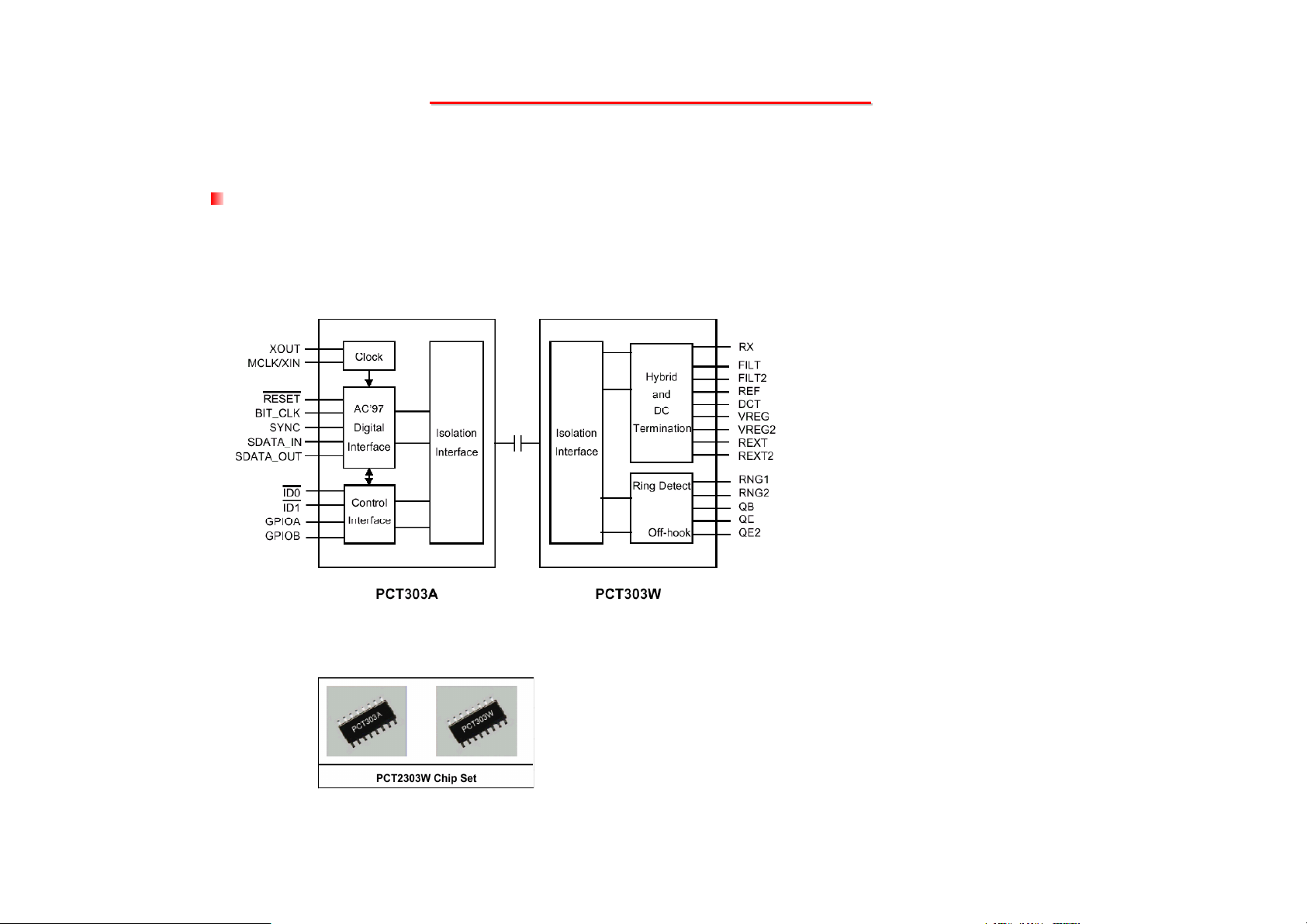
1.2.6 MDC: PCTel MODEM DAUGHTER CARD PCT2303W
The PCT2303W chipset is designed to meet the demand of this emerging worldwide AMR/MDC market. The
combination of PC-TEL’s well proven PCT2303W chipset and the HSP56TM MR software modem driver allows
systems manufactures to implement modem functions in PCs at a lower bill of materials (BOM) while maintaining
higher system performance.
PC-TEL has streamlined the traditional modem into the Host Signal Processing (HSP) solution. Operating with the
Pentium class processors, HSP becomes part of the host computer’s system software. It requires less power to operate
and less physical space than standard modem solutions. PC-TEL’s HSP modem is an easily integrated, cost-effective
communications solution that is flexible enough to carry you into the future.
The PCT2303W chip set is an integrated direct access arrangement (DAA) and Codec that provides a programmable
line interface to meet international telephone line requirements. The PCT2303W chip set is available in two 16-pin
small outline packages (AC’97 interface on PCT303A and phone-line interface on PCT303W). The chip set eliminates
the need for an AFE, an isolation transformer, relays, opto-isolators, and 2-to 4-wire hybrid. The PCT2303W chip set
dramatically reduces the number of discrete components and cost required to achieve compliance with international
regulatory requirements. The PCT2303W complies with AC’97 Interface specification Rev. 2.1.
The chip set is fully programmable to meet worldwide telephone line interface requirements including those described
by CTR21, NET4, JATE, FCC, and various country-specific PTT specifications. The programmable parameters of the
PCT2303W chip set include AC termination, DC termination, ringer impedance, and ringer threshold. The
PCT2303W chip set has been designed to meet stringent worldwide requirements for out-of-band energy, billing-tone
immunity, lightning surges, and safety requirements.
25
Page 27

8355 N/B MAINTENANCE
8355 N/B MAINTENANCE
Operating System Compatibility
Windows 98 / NT4.0 /Win 2K /Win XP
Compatibility
ITU-T V.90 56000,54667,53333,52000,50667,49333,48000,46667,45333,
42667,41333,40000,38667,37333,36000,34667,33333,32000,
30667,29333, 28000bps
K56Flex 56000,54000,52000,50000,48000,46000,44000,42000,40000,
38000,36000, 32000bps.
ITU-T V.34Annex 33600,31200 bps.
ITU-T V.34 28800 bps
ITU-T V.32bis 14400 bps
ITU-T V.32 9600,4800 bps
ITU-T V.22bis 2400 bps
ITU-T V.22 1200 bps
ITU-T V.21 300 bps
ITU-T V.23 1200/75 bps
ITU-T V.17 14400,12000,9600,7200 bps
ITU-T V.29 9600,7200 bps
ITU-T V.27ter 4800,2400 bps
26
Page 28

8355 N/B MAINTENANCE
8355 N/B MAINTENANCE
Bell 212A 1200 bps
Bell 103 300 bps
Modulation
56000bps(V90&K56Flex) PCM
33600 bps (V.34Annex) TCM
28800 bps (V.34) TCM
14400 bps (V.32bis) TCM
12000 bps (V.32bis) TCM
9600 bps (V.32bis) TCM
7200 bps (V.32bis) QAM
9600 bps (V.32) TCM, QAM
4800 bps (V.32) QAM
14400 bps (V.17) TCM
12000 bps (V.17) TCM
9600 bps (V.29) QAM
7200 bps (V.29) QAM
4800 bps (V.27ter) DPSK
2400 bps (V.27ter) DPSK
2400 bps (V.22bis) QAM
27
Page 29
8355 N/B MAINTENANCE
8355 N/B MAINTENANCE
1200/75bps (V.23) FSK
1200bps(V.22/Bell 212A) DPSK
300bps(V.21/Bell 103) FSK
Data Compression
V.42bis, MNP5
Error Correction
V.42 LAPM, MNP 2-4
DTE interface
DTMF Tone Frequency
Low Group Frequency (Hz)
697 770 852 941
High Group 1209 1 4 7 *
Frequency 1336 2 5 8 0
(Hz) 1477 3 6 9 #
1633 A B C D
DTMF signal level
28
Page 30

8355 N/B MAINTENANCE
8355 N/B MAINTENANCE
2.6.1.1 High group -10+/-2dBm
2.6.1.2 Low group -12+/-2dBm
Dialing Type
Tone or pulse dialing
Telephone Line interface
RJ-11
Return Loss
300HZ - 3400HZ >= 10db
Flow Control
XOFF/XON or RTS/CTS
Receive Level
-35 +/- 2dBm
29
Page 31
8355 N/B MAINTENANCE
8355 N/B MAINTENANCE
Transmit Level
>-15 dBm
Specification and features subject to change without notice!
2.6 MDC: PCTel MODEM DAUGHTER CARD PCT2303W
30
Page 32

8355 N/B MAINTENANCE
8355 N/B MAINTENANCE
1.2.7 VT6307L PCI 1394a Integrated Host Controller
1.2.7.1 Overview
The VT6307L IEEE 1394 OHCI Host Controller provides high performance serial connectivity. It implements the
Link and Phy layers for IEEE 1394-1995 High Performance Serial Bus a specification release 1.0 and 1394a P2000. It
is compliant with 1394 Open HCI 1.0 and 1.1 with DMA engine support for high performance data transfer via a 32-
bit bus master PCI host bus interface.
The VT6307L supports 100, 200 and 400 Mbit/sec transmission via an integrated 2-port PHY. The VT6307L services
two types of data packets: asynchronous and isochronous (real time). The 1394 link core performs arbitration
requesting, packet generation and checking, and bus cycle master operations. It also has root node capability and
performs retry operations.
The VT6307L is ready to provide industry-standard IEEE 1394 peripheral connections for desktop and mobile PC
platforms. Support for the VT6306 is built into Microsoft Windows 98, Windows ME, and Windows 2000.
1.2.7.2 Integrated 400 Mbit 2-Port PHY
Supports provisions of IEEE 1394-1995 Standard for High Performance Serial Bus and the P1394a P2000.
Fully interoperable with IEEE Std 1394-1995 devices
Provides two 1394a fully compliant cable ports at 100 / 200 / 400 Mbit per second
Host notification of PHY LinkOn events
Full 1394a P2000 Support includes:
31
Page 33

8355 N/B MAINTENANCE
8355 N/B MAINTENANCE
• Arbitrated short reset
• Enhanced priority arbitration
• Connection debounce
• Multispeed packet concatenation
• Ack accelerated arbitration
• Fly-by concatenation
• Per port disable, suspend, resume, through register write and remote command packet
• Remote access packet
• Boundary node short reset
• No PHY_ID wrap past 63
Logic performs bus initialization and arbitration functions
Encode and decode functions included for data-strobe bit-level encoding
Incoming data resynchronized to local clock.
24.576 MHz crystal oscillator and PLL provide TX/RX data at 100/200/400 Mbps and Link-Layer Controller
clock at 49.152 MHz.
Cable power presence monitoring.
Programmable node power class information for system power management
Fully Compliant 1394a P2000 PHY register map
Separate TPBIAS for each port
Cable ports monitor line conditions for active connection to remote node
Automatic power down inactive circuit and logic for low power application
Self power up reset and pinless PLL to reduce passive component counts on system
32
Page 34

8355 N/B MAINTENANCE
8355 N/B MAINTENANCE
Automatic configuration to single-port, two-port, and three-port applications; unused ports power down
automatically
Dedicated power supply pins separate from link core
2KV ESD protection
1.2.8 EMBEDDED CONTROLLER-H8
I. OVERVIEW
H8/300 CPU, a high-speed processor with an architecture featuring powerful bit-manipulation instructions, ideally
suited for real time control applications.
1.2.8.1 Main Features
CPU
Two-way generate register configuration
• Eight 16-bit registers, or
• Sixteen 8-bit registers
High-speed operation Maximum clock rate (ø clock): 16 MHz at 5 V, 12 MHz at 4 V or 10 MHz at 3V
• 8- or 16-bit register-register add/subtract: 125 ns (16 MHz), 167 ns (12 MHz), 200 ns (10 MHz)
• 8 x 8-bit multiply: 875 ns (16MHz), 1167 ns (12 MHz), 1400 ns (10 MHz)
• 16 ÷8-bit divide: 875 ns (16MHz), 1167 ns (12 MHz), 1400 ns (10 MHz)
Streamlined, concise instruction set
33
Page 35

8355 N/B MAINTENANCE
8355 N/B MAINTENANCE
• Instruction length: 2 or 4 bytes
• Register-register arithmetic and logic operations
• MOV instruction for data transfer between registers and memory
Instruction set features
• Multiply instruction (8 bits x 8 bits)
• Divide instruction (16 bits ÷8 bits)
• Bit-accumulator instructions
• Register-indirect specification of bit positions
Memory
1. 60-kbytes ROM with 2-kbytes RAM
Timer
One 16-bit free running timer
Two 8-bit timers
Two PWM timers (duty cycle 0-100%, resolution: 1/250)
One Watchdog timer
Interface
Two Serial Communication Interfaces
34
Page 36

8355 N/B MAINTENANCE
8355 N/B MAINTENANCE
One I2C bus interface
Host Interface
• 8-bit host interface port
• Three host interrupt requests (HIRQ1, HIRQ11, HIRQ12)
• Regular and fast A20 gate output
• Two register sets, each with two data registers and a status register
A/D converter –
10-bit resolutions
8 channels – single or scan mode (selectable)
Start of A/D conversion can be externally triggered
Sample-and-hold function
D/A converter –
8-bit resolutions
2 channels
I/O ports –
74 input/output lines (16 of which can drive LEDs)
8 input-only lines
35
Page 37

8355 N/B MAINTENANCE
8355 N/B MAINTENANCE
Interrupts –
9 external interrupt lines: NMI, IRQ0, to IRQ7
26 on-chip interrupt sources
Wait control –
Three selectable wait modes
Operating modes –
Expanded mode with on-chip ROM disabled (mode 1)
Expanded mode with on-chip ROM enabled (mode 2)
Single-chip mode (mode 3)
Power-down modes –
Sleep mode
Software Standby mode
Hardware Standby mode
Other features –
On-chip oscillator
36
Page 38

8355 N/B MAINTENANCE
8355 N/B MAINTENANCE
1.2.8.2 Features
Operating voltage: 2.4V~5.5V
32/34 bidirectional I/O lines
One 8-bit programmable timer counter with overflow
interrupts
Crystal or RC oscillator
Watchdog Timer
3K_16 program EPROM
160_8 data RAM
One external interrupt pin (shared with PC2)
HALT function and wake-up feature reduce power
consumption
Six-level subroutine nesting
Bit manipulation instructions
16-bit table read instructions
63 powerful instructions
All instructions in 1 or 2 machine cycles
20/28-pin SOP, 40-pin DIP, 48-pin SSOP package
37
Page 39

8355 N/B MAINTENANCE
8355 N/B MAINTENANCE
1.2.9 System Flash Memory (BIOS)
2 M bit Flash memory
Flashed by 5V only
User can upgrade the system BIOS in the future just running flash program.
1.2.10 Memory System
64MB, 128MB, 256MB, 512MB (x64) 200-Pin DDR SDRAM SODIMMs
JEDEC-standard 200-pin, small-outline, dual in-line memory module (SODIMM)
Utilizes 200 Mb/s and 266 Mb/s DDR SDRAM components
64MB (8 Meg x 64 [H]); 128MB (16 Meg x 64, [H] and [HD]); 256MB (32 Meg x 64 [HD]); 512MB (64 Meg x
64 [HD])
VDD= VDDQ= +2.5V ±0.2V
VDDSPD = +2.2V to +5.5V
2.5V I/O (SSTL_2 compatible)
Commands entered on each positive CK edge
DQS edge-aligned with data for READs; center-aligned with data for WRITEs
Internal, pipelined double data rate (DDR) architecture; two data accesses per clock cycle
Bidirectional data strobe (DQS) transmitted/received with data—i.e.,source-synchronous data capture
Differential clock inputs (CK and CK# - can be multiple clocks, CK0/CK0#, CK1/CK1#, etc.)
38
Page 40

8355 N/B MAINTENANCE
8355 N/B MAINTENANCE
Four internal device banks for concurrent operation
Selectable burst lengths: 2, 4, or 8
Auto precharge option
Auto Refresh and Self Refresh Modes
15.6µs (MT4VDDT864H, MT8VDDT1664HD), 7.8125µs (MT4VDDT1664H, MT8VDDT3264HD,
MT8VDDT6464HD) maximum average periodic refresh interval
Serial Presence Detect (SPD) with EEPROM
Fast data transfer rates PC2100 or PC1600
Selectable READ CAS latency for maximum compatibility
Gold-plated edge contacts
1.2.11 VT6103 FAST ETHERNET 10/100 1-PORT PHY/TRANSCEIVER
OVERVIEW
The VT6103 is a Physical Layer device for Ethernet 10Base-T and 100Base-TX using category 5 Unshielded, Type 1
Shielded, and Fiber Optic cables. This VLSI device is designed for easy implementation of 10 / 100 Mb/s Fast
Etherent LANs. It interfaces to a MAC through an MII interface ensuring interoperability between products from
different vendors.
PRODUCT FEATURES
Single Chip 100Base-TX / 10Base-T Physical Layer Solution
39
Page 41

8355 N/B MAINTENANCE
8355 N/B MAINTENANCE
Dual Speed – 100 / 10 Mbps
Half and Full Duplex
MII Interface to Ethernet Controller
MII Interface to Configuration & Status
Optional Repeater Interface
Auto Negotiation: 10 / 100, Full / Half Duplex
Meet All Applicable IEEE 802.3, 10Base-T and 100Base-Tx Standards
On Chip Wave Shaping – No External Filters Required
Adaptive Equalizer
Baseline Wander Correction
LED Outputs
• Link Status
• Duplex status
• Speed Status
• Collision
48 Pin SSOP Package
1.2.12 Cardbus/MediaReader Controller
Features
3.3V operation with 5V tolerant
40
Page 42

8355 N/B MAINTENANCE
8355 N/B MAINTENANCE
208-pin LQFP / 209-ball LFBGA package for CB710
PCI Interface
Compliant with PCI Local Bus Specification, Revision 2.2
PCI Bus Power Management Interface Specification, Revision 1.1
PCI Mobile Design Guide, Version 1.1
Advanced Configuration and Power Interface Specification, Revision 1.0
CardBus Interface
Compliant with PC Card Standard 8.0
Support Standardized Zoomed Video Register Model
Support CardBay PC card interface
Smart Card Interface
Compliant with PC/SC Specification 1.0
Support ISO7816 T=0 and T=1 asynchronous communication protocols
Two power enable pins to support 5V and 3V smart cards
Support programmable card clock frequencies
Programmable F and D parameters to support different data rates
One traffic LED pin.
41
Page 43

8355 N/B MAINTENANCE
8355 N/B MAINTENANCE
Secure Digital Interface
Compliant with SD Memory Card Specification Version 1.0
Support 4 parallel data lines
Has an optional reference clock source to control the operating clock frequency
Up to 10MByte/sec Read/Write rate when the optional reference clock source
Contains 16 Bytes of data buffer to regulate the data flow between PCI interface
interface
Support Write Protect Switch
Support Card Detect either by DAT3 or by dedicated Card Detect Switch
One Traffic LED pin
One power enable pin.
Memory Stick Interface
Compliant with Memory Stick Standard Format Specification Version 1.3
Has an optional reference clock source to control the operating clock frequency of Memory Stick
Up to 2.5MByte/sec Read/Write rate when the optional reference clock source is used
Contains 16 Bytes of data buffer to regulate the data flow between PCI interface and the Memory
42
Page 44

8355 N/B MAINTENANCE
8355 N/B MAINTENANCE
Stick interface
One Traffic LED pin
One power enable pin
SmartMedia Interface
Compliant with SmartMedia Standard 2000.
Compliant with SmartMedia Interface Library (SMIL) version 1.0
Two power enable pins to support 5V and 3V SmartMedia cards
Support hardware ECC (1-bit correction and 2-bits detection) generation
One traffic LED pin
Interrupt configuration
Supports parallel PCI interrupts
Supports parallel IRQ and parallel PCI interrupts
Supports serialized IRQ and parallel PCI interrupts
Supports serialized IRQ and PCI interrupts
Power Management Control Logic
Supports CLKRUN# protocol
43
Page 45

8355 N/B MAINTENANCE
8355 N/B MAINTENANCE
Supports SUSPEND#
Supports PCI PME# from D3, D2, D1 and D0
Supports PCI PME# from D3Cold
Supports D3STATE#
Supports Zoomed Video port.
Power Switch Interface
Supports parallel 4-wire power switch interface
Misc Control Logic
Supports socket activity LED
Supports 12 GPIOs and GPE#
Supports SPKROUT, CAUDIO and RIOUT#
Supports PCI LOCK
44
Page 46

8355 N/B MAINTENANCE
8355 N/B MAINTENANCE
1.2.13 SuperI/O-PC87393
General Description
National Semiconductor’s PC87393 of LPC SuperI/O devices is targeted for a wide range of portable applications.
PC99 and ACPI compliant, the PC87393 features an X-Bus Extension for read and write operations over the X-Bus, a
full IEEE 1284 Parallel Port with a Parallel Port Multiplexer (PPM) for external Floppy Disk Drive (FDD) support, a
Musical Instrument Digital Interface (MIDI) port, and a
Game port. Like all National LPC SuperI/O devices, the PC87393 offers a single-chip solution to the most commonly
used PC I/O peripherals.
The PC87393 also incorporates: a Floppy Disk Controller (FDC), two enhanced Serial Ports (UARTs), one with Fast
Infrared (FIR, IrDA 1.1 compliant), General-Purpose Input/Output (GPIO) support for a total of 32 ports, Interrupt
Serializer for Parallel IRQs and an enhanced WATCHDOG
TM
timer.
Outstanding Features
X-Bus Extension for read and write operations
LPC bus interface, based on Intel’s LPC Interface Specification Rev. 1.01, February 1999 (supports CLKRUN
and LPCPD signals) and Intel FWH transactions
PC99 and ACPI compliant
Serial IRQ support (15 options)
Interrupt Serializer (four Parallel IRQs to Serial IRQ)
45
Page 47

8355 N/B MAINTENANCE
8355 N/B MAINTENANCE
PPM for external FDD signal support
MIDI interface compatible with MPU-401 UART mode
Game port inputs for up to two joysticks
Protection features, including GPIO lock and pin configuration lock
32 GPIO ports (16 standard, 16 with Assert IRQ/SMI)
5V tolerant and back-drive protected pins (except LPC bus pins)
100-pin TQFP Package
46
Page 48
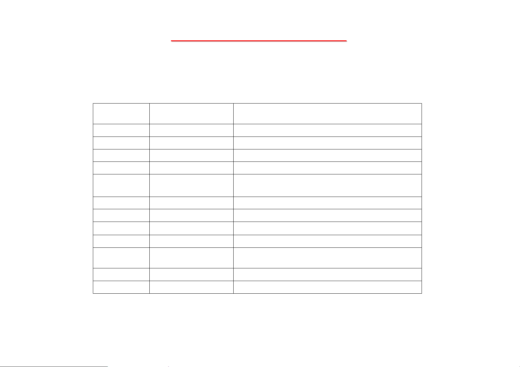
1.3 Other Functions
1.3.1 Hot Key Function
8355 N/B MAINTENANCE
8355 N/B MAINTENANCE
Keys
combination
Fn + F1
Fn + F2
Fn + F3
Fn + F4
Fn + F10
Fn + F11
Fn + F12
Feature
Reserve
Reserve
Reserve
Reserve
Display switchFn + F5
Brightness downFn + F6
Brightness upFn + F7
ReservedFn + F9
Beep toggle
LCD panel toggle on/off
Meaning
LCD->CRT->LCD&CRT, TV-out will be not TV present.
TV->CRT->TV&CRT, TV-out is connected.
Adjust LCD panel backlight darkness.
Adjust LCD panel backlight lightness.
Toggle LCD brightness maximum or user settingMAX brightness toggleFn + F8
Toggle to enable/mute the “Battery Low Warning” Beep soundBattery Low Warning
Toggle LCD panel on or off.
System sleep button function.System sleep
47
Page 49

8355 N/B MAINTENANCE
8355 N/B MAINTENANCE
1.3.2 Power ON/OFF/Suspend/Resume Button
APM mode
At APM mode, Power button is on/off system power.
ACPI mode
At ACPI mode. Power button behavior was set by windows power management control panel.
You could set “standby” , “power off” or “hibernate”(must enable hibernate function in power management) to power
button function. Continue pushing power button over 4 seconds will force system off at ACPI mode.
1.3.3 Cover Switch
System automatically provides power saving by monitoring Cover Switch. It will save battery power and prolong the
usage time when user closes the notebook cover.
At ACPI mode there are four functions to be chosen at windows power management control panel.
1. None
2. Standby
3. Off
4. Hibernate (must enable hibernate function in power management)
48
Page 50

8355 N/B MAINTENANCE
8355 N/B MAINTENANCE
1.3.4 LED Indicators
System has eight status LED indicators at front side which to display system activity. From left to right that indicate,
AC POWER, BATTERY POWER, BATTERY STATUS, WIRELESS LAN, CD-ROM, HARD DISK, NUM
LOCK, CAPS LOCK and SCROLL LOCK.
AC POWER: This LED lights green when AC is powering the notebook, and flash (on 1 second, off 1 second) when
Suspend to DRAM is active using AC power. The LED is off when the notebook is off or powered by batteries.
BATTERY POWER: This LED lights green when the notebook is being powered by Battery, and flash (on 1 second,
off 1 second) when Suspend to DRAM is active using Battery power. The LED is off when the notebook is off or
powered by batteries, or when Suspend to Disk.
BATTERY STATUS: During normal operation, this LED stays off as long as the battery is charged. When the
battery charge drops to 10% of capacity, the LED lights red, flashes per 1 second and beeps per 2 second. When AC
is connected, this indicator glows green if the battery pack is fully charged or orange (amber) if the battery is being
charged.
1.3.5 Fan power on/off management
FAN is controlled by H8 embedded controller-using AD2201 to sense CPU temperature and PWM control fan speed.
Fan speed is depended on CPU temperature. Higher CPU temperature faster Fan Speed.
49
Page 51

1.3.6 CMOS Battery
CR2032 3V 220mAh lithium battery
When AC in or system main battery inside, CMOS battery will consume no power.
AC or main battery not exists, CMOS battery life at less (220mAh/5.8uA) 4 years.
Battery was put in battery holder, can be replaced.
1.3.7 I/O Port
Bi-directional Parallel Port (EPP/ECP) x 1
USB port (2.0, backward compatible with USB1.1) x 4
8355 N/B MAINTENANCE
8355 N/B MAINTENANCE
RJ-11 port x 1
RJ-45 port x 1
IR port x 1, complies with IrDA 1.1
DC input x 1
VGA monitor port x1
Audio-out x 1 (S/P DIF)
Mic-in x 1
Hardware Volume Control
S Video TV-Out x 1 (NTSC/PAL)
50
Page 52

8355 N/B MAINTENANCE
8355 N/B MAINTENANCE
IEEE1394a x 1
1.3.8 Mini PCI (type III B)Battery current limit and learning
Implanted H/W current limit and battery learning circuit to enhance protection of battery.
51
Page 53
8355 N/B MAINTENANCE
8355 N/B MAINTENANCE
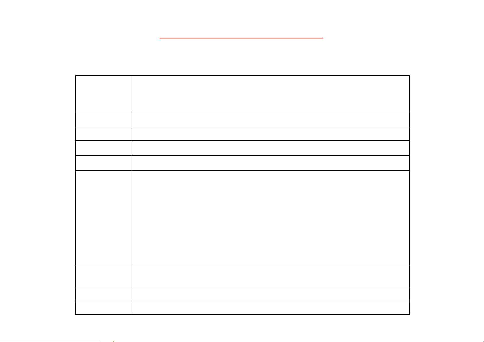
1.4 Peripheral Components
ROM Drive
HDD
FDD
Display
Keyboard
I/O Port
Communication
- 12.7mm Height
- 24X CD ROM Drive
- 8X DVD ROM Drive
- 24X10X8X24 Combo or above
- Super Combo DVD-RW module
- 2.5" 9.5 mm height: 20/30/40/60 GB; Support Ultra DMA 66/100/133
- Changeable for Distributor
- Support External FDD w/z USB I/F; 3.5 Format for 720KB/1.2MB/1.44MB
- 14.1” XGA TFT Display; Resolution: 1024x768
- 15” XGA/ SXGA+ TFT Display; Resolution: 1024X768 /1400x1050
- 19mm key pitch/ 3.0mm key stroke/ 307mm length
- Windows Logo Key x 1; Application Key x 1
- Bi-directional Parallel Port (EPP/ECP) x 1
- USB port (2.0, backward compatible with USB1.1) x 4
- RJ-11 port x 1
- RJ-45 port x 1
- IR port x 1, complies with IrDA 1.1
- DC input x 1
- VGA monitor port x1
- Audio-out x 1 (S/P DIF)
- Mic-in x 1
- Hardware Volume Control
- S Video TV-Out x 1 (NTSC/PAL)
- IEEE1394a x 1
- Mini PCI (type III B)
- Built-in 56Kbps V.90 modem
- Built-in 10/100 M based-T LAN
- One Mini PCI slot and one antenna reserved for wireless LAN(Type III B)
Battery
AC adapter
- 12 cell (2200mAH/3.7V) Li-ion standard
- Universal AC adapter 150W ; Input: 100-240V, 50/60Hz AC (support power on charge)
52
Page 54

8355 N/B MAINTENANCE
8355 N/B MAINTENANCE
1.5 Power Management
The 8355 system has built in several power saving modes to prolong the battery usage for mobile purpose. User can
enable and configure different degrees of power management modes via ROM CMOS setup (booting by pressing F2
key). Following are the descriptions of the power management modes supported.
1.5.1 System Management Mode
Full on mode
In this mode, each device is running with the maximal speed. CPU clock is up to its maximum.
Doze Mode
In this mode, CPU will be toggling between on & stop grant mode either. The technology is clock throttling. This
can save battery power without loosing much computing capability.
The CPU power consumption and temperature is lower in this mode.
Standby mode
The most chipset of the system is entering power down mode for more power saving. In this mode, the following is
the status of each device:
CPU: Stop grant
LCD: backlight off
53
Page 55

8355 N/B MAINTENANCE
8355 N/B MAINTENANCE
HDD: spin down
Suspend to DRAM
The most chipset of the system is entering power down mode for more power saving. In this mode, the following is
the status of each device:
Suspend to DRAM
CPU: off
VT8235: Partial off
VGA: Suspend
PCMCIA: Suspend
Audio: off
SDRAM: self refresh
Suspend to HDD
All devices are stopped clock and power-down
System status is saved in HDD
All system status will be restored when powered on again
54
Page 56

8355 N/B MAINTENANCE
8355 N/B MAINTENANCE
1.5.2 Other Power Management Functions
HDD & Video Access
System has the ability to monitor video and hard disk activity. User can enable monitoring function for video
and/or hard disk individually. When there is no video and/or hard disk activity, system will enter next PMU state
depending on the application. When the VGA activity monitoring is enabled, the performance of the system will
have some impact.
55
Page 57
8355 N/B MAINTENANCE
8355 N/B MAINTENANCE
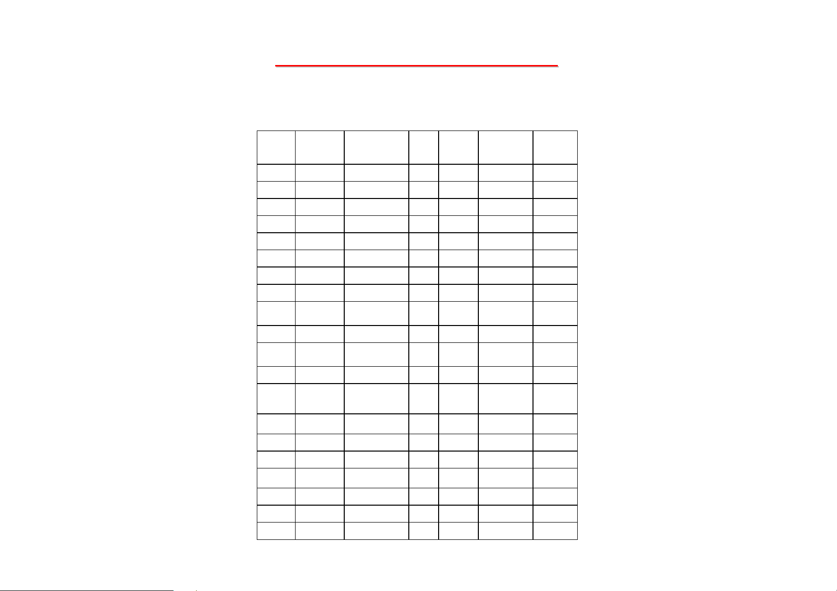
1.6 Appendix 1: VT 8235 GPIO Definition
Signal
Name
GPI0 RESERVE I RTC Hi-Z TTL
GPI1 RESERVE I AUX Hi-Z TTL
GPI2 EXTSMI# EXTSMI# I AUX Defined TTL
GPI3 RING# WAKE_UP# I AUX Defined TTL
GPI4 LID# RESERVE I AUX Defined TTL
GPI5 BATLOW# SCI# I AUX Defined TTL
GPI6 AGPBZ# RESERVE I MAIN Defined TTL
GPI7 REG5# RESERVE I MAIN Hi-Z TTL
GPI16
GPI17 CPUMISS RESERVE I MAIN Defined TTL
GPI18
GPI19 IORDY RESERVE I MAIN Defined TTL
GPO0 RESERVE O AUX H TTL
GPO1 SUSA# SUSA# O AUX Defined TTL
MUX
Function
INTRUDE
R# RESERVE I RTC Defined TTL
THRM# /
AOLGPI THRM# I MAIN Defined TTL
Mitac
Definition
Buffer
Type
Power
Plane
Default
Value Type
GPO2 SUSB# SUSB# O AUX Defined TTL
GPO3 SUSST1# SB_SUSST# O AUX Defined TTL
GPO4 SUSCLK RESERVE O AUX Defined TTL
GPO5 CPUSTP# RESERVE O MAIN Defined TTL
GPO6 PCISTP# PCISTOP# O MAIN Defined TTL
GPO7 GNT5# RESERVE O MAIN Defined TTL
56
Page 58

8355 N/B MAINTENANCE
8355 N/B MAINTENANCE
Continued to the previous table
GPIO8
GPIO9 PCREQB MB_ID1 I/O MAIN Hi-Z TTL
GPIO10 KBD_CS0 I/O MAIN Hi-Z TTL
GPIO11 KBD_CS1 I/O MAIN Hi-Z TTL
GPIO12
GPIO13
GPIO14 INTG# CRT_IN I/O MAIN Hi-Z TTL
GPIO15 INTH# MPCIACT# I/O MAIN Hi-Z TTL
GPIO20
GPIO21
PCREQA /
VGATE MB_ID0 I/O MAIN Hi-Z TTL
INTE# /
PCGNTA RESERVE I/O MAIN Hi-Z TTL
INTF# /
PCGNTB RESERVE I/O MAIN Hi-Z TTL
ACSDIN2 /
PCS0# RESERVE I/O MAIN Hi-Z OD
ACSDIN3 /
PCS1# /
SLPBTN# RESERVE I/O MAIN Hi-Z OD
GPIO22 GHI# FAN3_SPDCTR I/O MAIN Hi-Z OD
GPIO23 DPSLP# LDTSTOP# I/O MAIN Hi-Z OD
GPIO24 GPIOA SPKR_MUTE# I/O MAIN Hi-Z OD/TTL
GPIO25 GPIOC FAN2_SPDCTR I/O MAIN Hi-Z OD/TTL
GPIO26 SMBDT2 RESERVE I/O AUX Hi-Z OD
GPIO27 SMBCK2 RESERVE I/O AUX Hi-Z OD
GPIO28 VIDSEL RESERVE I/O MAIN Hi-Z OD
GPIO29 VRDSLP RESERVE I/O MAIN Hi-Z OD
GPIO30 GPIOD FAN1_SPDCTR I/O MAIN Hi-Z OD/TTL
GPIO31 GPIOE MINIPCI_PD I/O MAIN Hi-Z OD/TTL
57
Page 59
8355 N/B MAINTENANCE
8355 N/B MAINTENANCE
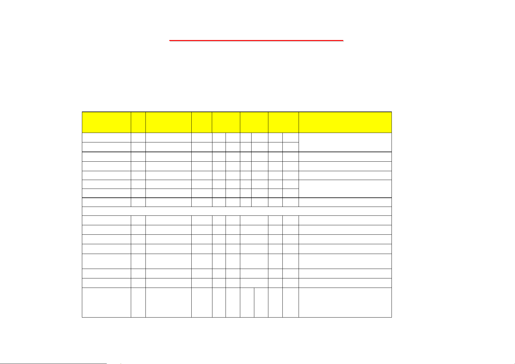
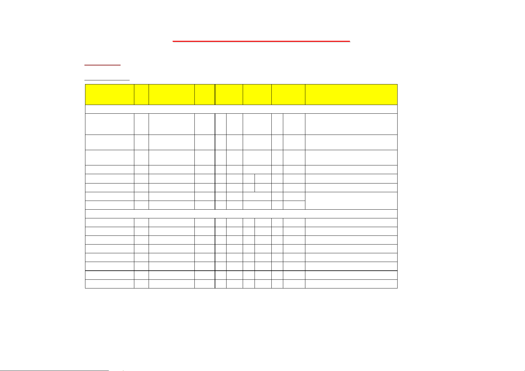
1.7 Appendix 2: H8 Pins Definition
Hitachi H8 3437S to VT8235 pin function definitions for Insyde code
the shadowed block is the selected function
Name Pin H8 Pin Definitions During
MD0 6 H8_MODE0 I↑
MD1 5 H8_MODE1 I↑
STBY# 8 H8_STBY# I↑
NMI# 7 PWRBTN# I↑
RESET# 1 H8_RESET# I I LH I H I H H8 chip reset
XTAL 2 Crystal I I I I
EXTAL 3 Crystal I I I I
RESET OUT# 100 RESERVE O O O O
Port A CMOS input level (input high min=3.5v, input low max=1.0v)
PA0 48 LID#
PA1 47 ADEN# T↑ I H/L I I H/L AC adaptor in detect
PA2 31 CARD_RI#
PA3 30 BATT DEAD#
PA4 21 H8 SUSC
PA5 20 H8 SUSC#
PA6 11 BAT_CLK
PA7 10 H8_SUSB
RESE
T
T↑
T↑
T↑
T↑
T↑
T↑
T↑
After
RESET/O
FF
I H I H I H
I H I H I H
I H I H I H H8 Hardware Standby input pull high
I H I HLH I H Power button
I H I I H
I H I I H Rin g detect
I H I I H Battery low low detect
I H I I L System resume from S4 soft off through
I L I I H System to S4 soft off
I L I I H
I H I L I H Invert from SUSA# to wake up H8 when
ON STANDBY Functi on
H
H mode3 single chip mode
Crystal input
RTC Alarm
system resumed by MDC modem and
internal LAN.
Inform system power management status
58
Page 60
Charging 1
PCI reset gate
8355 N/B MAINTENANCE
8355 N/B MAINTENANCE
Name Pin H8 Pin Definitions During
Port B TTL input voltage (input high min=2v, input low max=0.8v)
PB0 91 SB_PWRBTN# T O L LHL O Keep H Power button trigger via8231 on /off
PB1 90 H8_WAKE UP# T O H O O Keep H Wake up SB at ACPI mode
PB2 81 LEARNING T O O Keep H Power button trigger via8231 on
PB3 80 CHARGING_RP T O O O Keep Battery charge control
PB4 69 VDD5 SW
PB5 68 H8_PWROK T O L O LH O Keep H
PB6 58 RESERVE T O O O Keep
PB7 57 RESERVE T O O O Keep
Port 1 TTL input voltage (input high min=2v, input low max=0.8v)
P10/A0 79 KB OUT0 L O L O LH O Keep L Key matrix scan output 0
P11/A1 78 KB OUT1 L O L O LH O Keep L Key matrix scan output 1
P12/A2 77 KB OUT2 L O L O LH O Keep L Key matrix scan output 2
P13/A3 76 KB OUT3 L O L O LH O Keep L Key matrix scan output 3
P14/A4 75 KB OUT4 L O L O LH O Keep L Key matrix scan output 4
P15/A5 74 KB OUT5 L O L O LH O Keep L Key matrix scan output 5
P16/A6 73 KB OUT6 T O L O LH O Keep L Key matrix scan output 6
P17/A7 72 KB OUT7 T O L O LH O Keep L Key matrix scan output 7
RESE
T
T↓
After
RESET/O
FF
O LLH O H O Keep H H8 vdd5 power source switch
ON STANDBY Function
Duplicate Power BTN#
5→3V
5→3V?
5→3V
59
Page 61
8355 N/B MAINTENANCE
8355 N/B MAINTENANCE
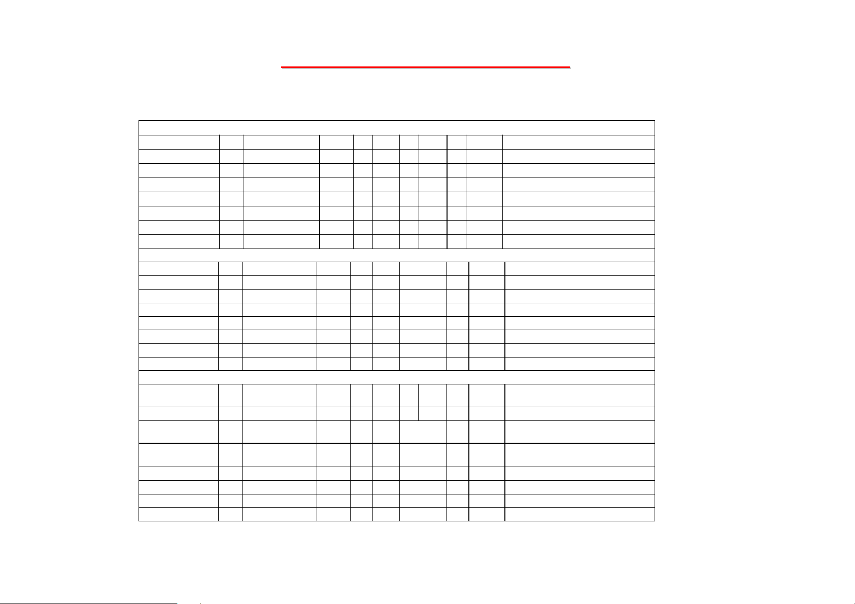
Continued to the previous table
Port 2 TTL input voltage (input high min=2v, input low max=0.8v)
P20/A8 67 KB OUT8 L O L O LH O Keep L Key matrix scan output 8
P21/A9 66 KB OUT9 L O L O LH O Keep L Key matrix scan output 9
P22/A10 65 KB OUT10 L O L O LH O Keep L Key matrix scan output 10
P23/A11 64 KB OUT11 L O 0 O LH O Keep L Key matrix scan output 11
P24/A12 63 KB OUT12 L O 0 O LH O Keep L Key matrix scan output 12
P25/A13 62 KB OUT13 L O 0 O LH O Keep L Key matrix scan output 13
P26/A14 61 KB OUT14 L O 0 O LH O Keep L Key matrix scan output 14
P27/A15 60 KB OUT15 L O 0 O LH O Keep L Key matrix scan output 15
Port 3 TTL input voltage (input high min=2v, input low max=0.8v)
P30/HDB0/D0 82 ISA SD0 T I/O I/O I/O Keep ISA DATA bit 0
P31/HDB1/D1 83 ISA SD1 T I/O I/O I/O Keep ISA DATA bit 1
P32/HDB2/D2 84 ISA SD2 T I/O I/O I/O Keep ISA DATA bit 2
P33/HDB3/D3 85 ISA SD3 T I/O I/O I/O Keep ISA DATA bit 3
P34/HDB4/D4 86 ISA SD4 T I/O I/O I/O Keep ISA DATA bit 4
P35/HDB5/D5 87 ISA SD5 T I/O I/O I/O Keep ISA DATA bit 5
P36/HDB6/D6 88 ISA SD6 T I/O I/O I/O Keep ISA DATA bit 6
P37/HDB7/D7 89 ISA SD7 T I/O I/O I/O Keep ISA DATA bit 7
Port 4 TTL input voltage (input high min=2v, input low max=0.8v)
P40/TMCI0 49 H8 PWRON T↓
P41/TMO0 50 H8 THRM# T O L O H O Keep H Thermal throttling control to Southbridge
P42/TMRI0 51 SCI#/
FAN SPD SW
P43/TMCI1/HIRQ1 52 SCI#/
FAN SPEED
P44/TMCO1/HIRQ1 53 ISA IRQ1 T O 0 O O Keep Keyboard IRQ1
P45/TMRI1/HIRQ1 54 ISA IRQ12 T O 0 O O Keep PS2 mouse IRQ12
P46/PWM0 55 FAN ON#0 T O 1 O O Keep Fan power PWM control
P47/PWM1 56 FAN ON#1 T O 1 O O Keep Fan power PWM control
T O H O Keep SCI output and Fan Speed Tachometer
T O/I O O Keep Need invert to SCI# sending to SB
O L O LH O Keep System power on, need pull down to define
initial state during reset
Switch
5→3V/ Fan speed tachometer
60
Page 62
8355 N/B MAINTENANCE
8355 N/B MAINTENANCE
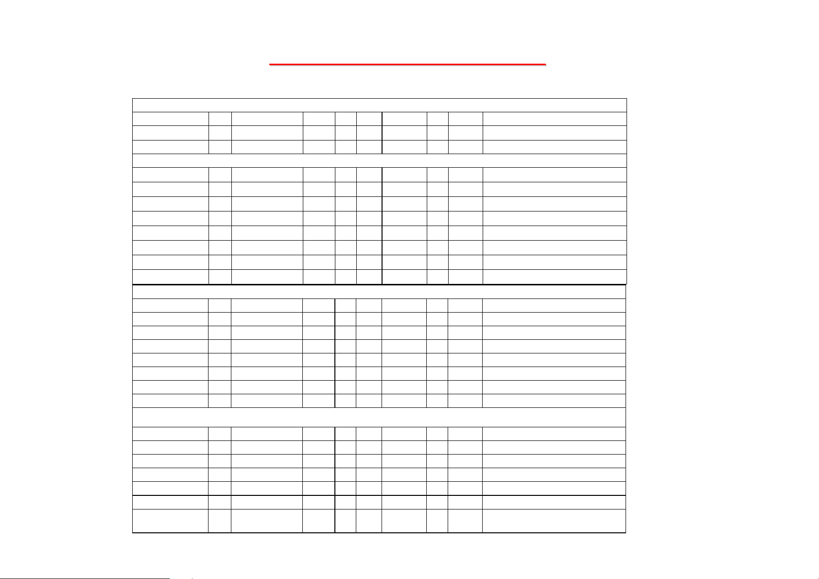
Continued to the previous table
Port 5 TTL input voltage (input high min=2v, input low max=0.8v)
P50/TXD0 14 LED DATA T O O O Keep LED indicator shift data
P51/RXD0 13 H8 SMI# T O O O Keep
P52/SCK0 12 LED CLK T O O O Keep LED indicator shift clock
Port 6 Schmitt trigger input voltage (min=1.0v max=3.5v)
P60/KEYIN0/FTCI 26 KEY IN0
P61/KEYIN1/FTOA 27 KEY IN1
P62/KEYIN2/FTIA 28 KEY IN2
P63/KEYIN3/FTIB 29 KEY IN3
P64/KEYIN4/FTIC 32 KEY IN4
P65/KEYIN5/FTID 33 KEY IN5
P66/KEYIN6/IRQ6 34 KEY IN6
P67/KEYIN7/IRQ7 35 KEY IN7
Port 7 TTL input voltage (input high min=2v, input low max=0.8v)
P70/AN0 38 BAT VOLT1 T I I I T Battery voltage measure
P71/AN1 39 I_LIMIT T I I I T
P72/AN2 40 H8_I_DISCHG T I I I T Moni tor system on/ off state
P73/AN3 41 H8_I_CHG T I I I T
P74/AN4 42 BAT TEMP1 T I I I T Battery thermister temperature
P75/AN5 43 VCC CORE T I I I T
P76/AN6/DA0 44 H8_I_CTR T O O O T Charging current adjust
P77/AN7/DA1 45 BL ADJ T O O O T Backlight inverter brightness adjust
T↑
T↑
T↑
T↑
T↑
T↑
T↑
T↑
I I I Keep Key matrix input 0 need pull high
I I I Keep Key matrix input 1 need pull high
I I I Keep Key matrix input 2 need pull high
I I I Keep Key matrix input 3 need pull high
I I I Keep Key matrix input 4 need pull high
I I I Keep Key matrix input 5 need pull high
I I I Keep Key matrix input 6 need pull high
I I I Keep Key matrix input 7 need pull high
External SMI# 5→3V
Port 8 TTL input voltage (input high min=2v, input low max=0.8v)
P80/HA0 93 ISA SA2 T I I I Keep
P81/GA20 94 RESERVE T O O O Keep
P82/CS1 95 H8 KBCS# T I I I Keep IO port 60/64 chip select
P83 /IOR 96 ISA IOR# T I I I Keep ISA I/ O read#
P84 /IRQ2/TXD1 97 ISA IOW# T I I I Keep ISA I/ O write
P85/IRQ4/RXD1 98 H8 MCCS# T I I I Keep IO port 62/66 chip select
P86/IRQ5/SCK1 99 BAT CLK
T↑
I/O I/O I/O Keep SM BUS clock need pu ll h igh
5→3V
61
Page 63
8355 N/B MAINTENANCE
8355 N/B MAINTENANCE
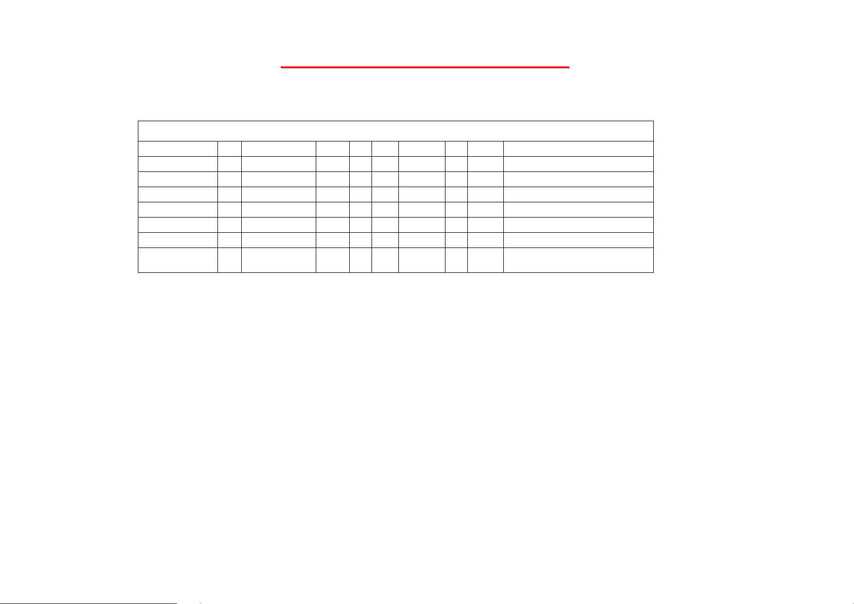
Continued to the previous table
Port 9 TTL input voltage (input high min=2v, input low max=0.8v)
P90/IRQ2/ESC2 25 PORT90
P91/IRQ1/EIOW 24 PORT91
P92/IRQ0 23 H8/T CLK
P93/RD 22 RSMRST
P94/WR 19 RESERVE
P95/AS 18 T DATA
P96/0 17 H8_ENABKL
P97/WAIT/SDA 16 BAT DATA
T↑
T↑
T↑
T↑
T↑
T↑
T↑
T↑
↑ Pull High
↓ Pull Low
5→3V Level shift
I/O I/O I/O Keep
I/O I/O I/O Keep
I/O I/O I/O Keep need pull high
I/O I/O I/O Keep
I/O I/O I/O Keep need pull high
I/O I/O I/O Keep need pull high
I I I T Read H8 send A20gate status
I/O I/O I/O Keep SM BUS clock need pull high
5→3V
62
Page 64
8355 N/B MAINTENANCE
8355 N/B MAINTENANCE
1.8 Appendix 3: 8355 product spec.
- AMD ClawHammer K8 processor with uPGA Package
CPU
- 2700+/3000+/3300+/3600+/3900+/4200+
- FSB 800MHz
Core Logic
L2 Cache
System BIOS
Memory
ROM Drive
HDD
FDD
Display
Video Controller
Keyboard
- VIA K8T800 + VT8235
- 512KB OD
- Insyde 256 KB Flash EPROM (Include System BIOS and VGA BIOS)
- ACPI 2.0; DMI 2.3.1 compliant
- Plug & Play capability
- 0MB on board; Expandable up to 1024MB
- Expandable with combination of optional 128/256/512 MB memory
- 200-pin DDR 266/333/400 DRAM Memory Module x2, PC-2100/2700/3200 specification
- 12.7mm Height
- 24X CD ROM Drive
- 8X DVD ROM Drive
- 24X10X8X24 Combo or above
- Super Combo DVD-RW module
- 2.5" 9.5 mm height: 20/30/40/60 GB; Support Ultra DMA 66/100/133
- Changeable for Distributor
- Support External FDD w/z USB I/F; 3.5 Format for 720KB/1.2MB/1.44MB
- 14.1” XGA TFT Display; Resolution: 1024x768
- 15” XGA/ SXGA+ TFT Display; Resolution: 1024X768 /1400x1050
- ATI M10P with 64MB External VRAM (Reserve for 128MB VRAM)
- 19mm key pitch/ 3.0mm key stroke/ 307mm length
- Windows Logo Key x 1; Application Key x 1
Button
Pointing Device
PCMCIA
4 in 1 Card reader
- 1x Wireless RF switch button with LED
- Glide pad with 2x buttons and 4 direction scroll button
- TypeII X1 Without ZV -Cardbus Support
- Card Reader SD/SM/MMC
63
Page 65
8355 N/B MAINTENANCE
8355 N/B MAINTENANCE
Continued to the previous table
Indictor
Audio System
I/O Port
Communication
- 3 LEDs for Power/Battery status (on display housing )
- 1 LED for Radio wave status Power LED (with switch button)
- 5 LEDs for HDD Access, ODD Access , Num lock, Cap lock and Scroll Lock .
- 1 LED for Card reader status
- Sound Blaster Pro compatible
- AC97 V2.1 Codec
- Built-in Mono Microphone
- 2X Speaker (w/z sound chamber)
- Bi-directional Parallel Port (EPP/ECP) x 1
- USB port (2.0, backward compatible with USB1.1) x 4
- RJ-11 port x 1
- RJ-45 port x 1
- IR port x 1, complies with IrDA 1.1
- DC input x 1
- VGA monitor port x1
- Audio-out x 1 (S/P DIF)
- Mic-in x 1
- Hardware Volume Control
- S Video TV-Out x 1 (NTSC/PAL)
- IEEE1394a x 1
- Mini PCI (type III B)
- Built-in 56Kbps V.90 modem
- Built-in 10/100 M based-T LAN
- One Mini PCI slot and one antenna reserved for wireless LAN(Type III B)
AC adapter
Battery
Dimensions
Weight
Accessories
Manual Printings
- Universal AC adapter 150W (3 pins); Input: 100-240V, 50/60Hz AC (support power on charge)
- 12 cell (2200mAH/3.7V) Li-ion standard
- 332x285x37.1~41.1(max)
- 3.6kg
- Power Cord, AC Adapter, RJ-11 Phone Cable, Manual, System Driver CD-Title
- EN, GR, CH, Pan-EU
64
Page 66
8355 N/B MAINTENANCE
8355 N/B MAINTENANCE
Continued to the previous table
Agency
Architecture
Options
- FCC, CE, UL, TUV, CB, BSMI
- Support PC2001 Specification, Designed for Windows XP(driver ready for 98,ME, and 2000)
- 128/256/512MB DDR SDRAM, AC Adapter w/o Power Cord, Notebook Carry Bag
65
Page 67
8355 N/B MAINTENANCE
8355 N/B MAINTENANCE
2. System View and Disassembly
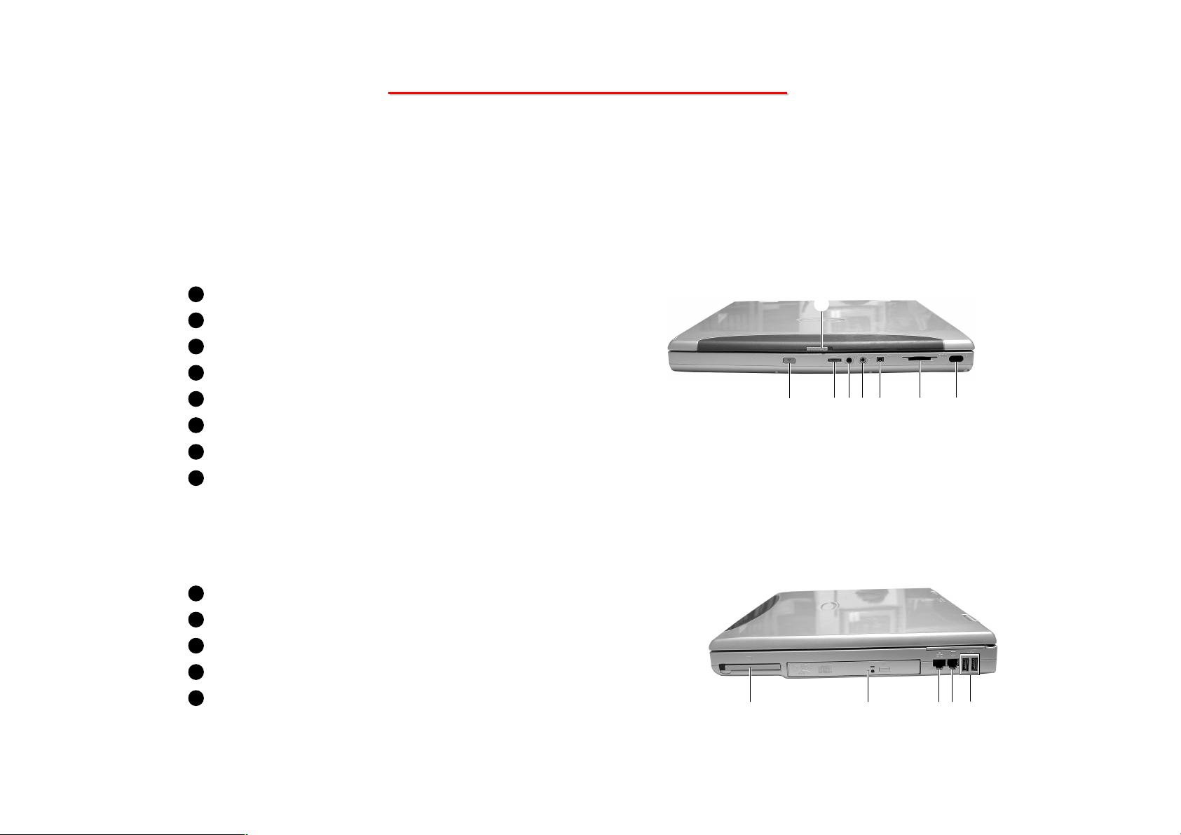
2.1 System View
2.1.1 Front View
1
Hold Switch
2
Volume Control
3
Audio Output
4
Microphone Input
5
1394 port
6
Card Reader Slot
7
IR Module
8
Top Cover Latch
2.1.2 Left-side View
1
PCMCIA Card Socket
2
CD/DVD-ROM Drive
3
RJ-11 Connector
4
RJ-45 Connector
5
USB Port*2
66
Page 68
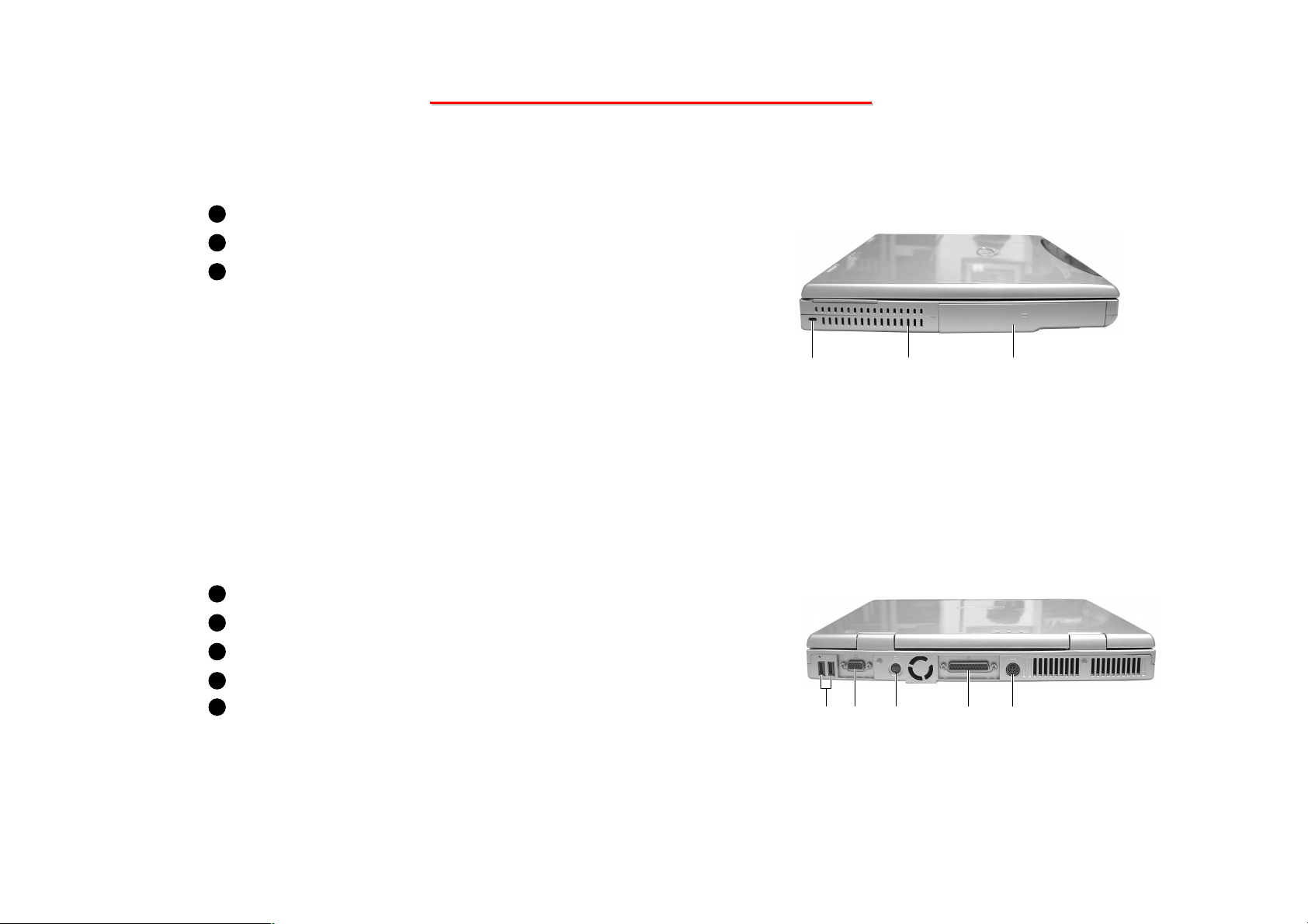
8355 N/B MAINTENANCE
2.1.3 Right-side View
1
Kensington Lock
2
Ventilation Openings
3
Battery pack
2.1.4 Rear View
8355 N/B MAINTENANCE
1
USB Port*2
2
VGA Port
3
S-Video Output Connector
4
Parallel Port
5
Power Connector
67
Page 69
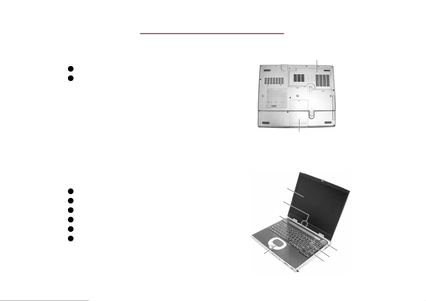
2.1.5 Bottom View
1
CPU Cover
2
Hard Disk Drive Cover
2.1.6 Top View
8355 N/B MAINTENANCE
8355 N/B MAINTENANCE
1
Stereo Speaker
2
Touch Pad
3
Power Button
4
Keyboard
5
Device Indicators
6
LCD Screen
68
Page 70

8355 N/B MAINTENANCE
8355 N/B MAINTENANCE
2.2 System Disassembly
The section discusses at length each major component for disassembly/reassembly and show corresponding
illustrations. Use the chart below to determine the disassembly sequence for removing components from the
notebook.
NOTE: 1. Before you start to install/replace these modules, disconnect all peripheral devices and make sure
the notebook is not turned on or connected to AC power.
2. During disassembly, 1) Label each cable as you disconnect it, noting its position and routing;
2) Keep all the screws.
69
Page 71

8355 N/B MAINTENANCE
8355 N/B MAINTENANCE
2.2.1 Battery Pack
2.2.2 Keyboard
2.2.3 CPU
Modular Components
2.2.4 HDD Disk Drive
2.2.5 CD/DVD-ROM Drive
2.2.6 DDR SDRAM
2.2.7 LCD Assembly
NOTEBOOK
LCD Assembly Components
Base Unit Components
2.2.8 Inverter Board
2.2.9 LCD Panel
2.2.10 System Board
2.2.11 Modem Card
2.2.12 Touch Pad
70
Page 72
8355 N/B MAINTENANCE
8355 N/B MAINTENANCE
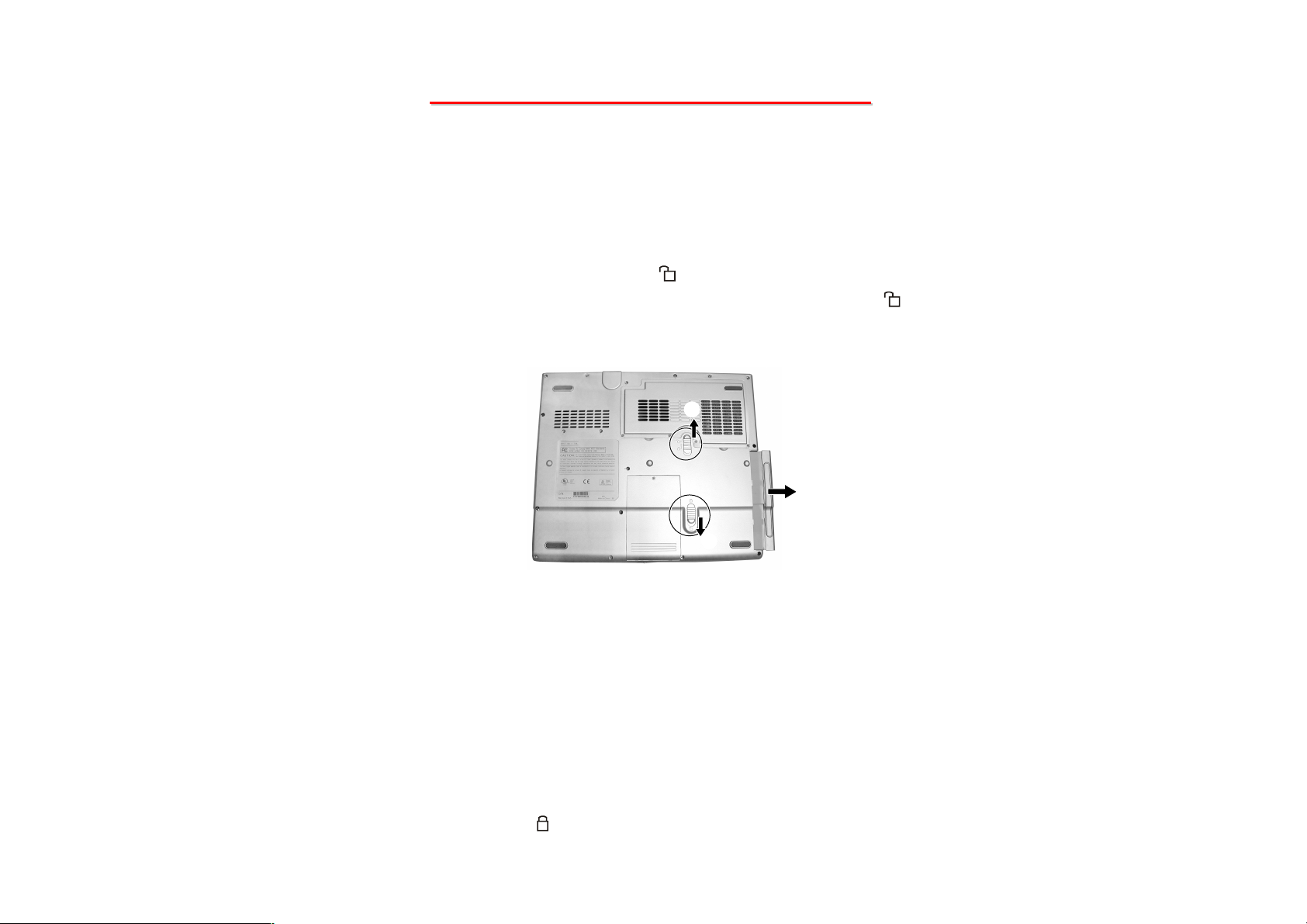
2.2.1 Battery Pack
Disassembly
1. Carefully put the notebook upside down.
2. Slide and keep the upper release lever on “unlock” ( ) position (), and then pull the battery pack out of the
compartment () while sliding the lower release lever downwards to “unlock” ( ) position (). (Figure 2-1)
Figure 2-1 Remove the battery pack
Reassembly
1. Replace the battery pack into the compartment. The battery pack should be correctly connected when you hear a
clicking sound.
2. Slide the release lever to the “lock” ( ) position.
71
Page 73
8355 N/B MAINTENANCE
8355 N/B MAINTENANCE
2.2.2 Keyboard
Disassembly
1. Remove the battery pack. (See section 2.2.1 Disassembly)
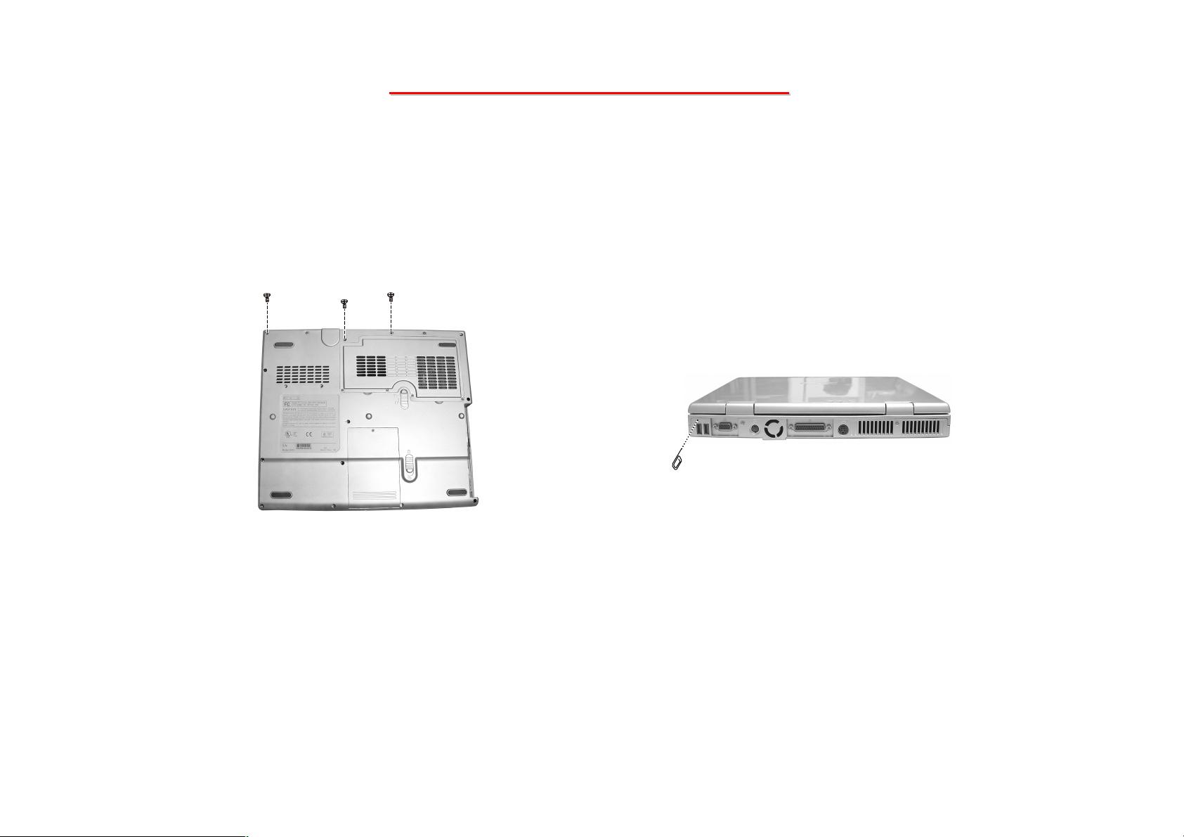
2. Remove three screws that fastening the keyboard cover on the bottom of the notebook. (Figure 2-2)
Figure 2-2 Remove three screws Figure 2-3 Insert a rod easy to remove
3. Insert a small rod, such as a straightened paper clip, into the eject hole near the USB ports of the notebook.
(Figure 2-3)
72
Page 74
8355 N/B MAINTENANCE
8355 N/B MAINTENANCE
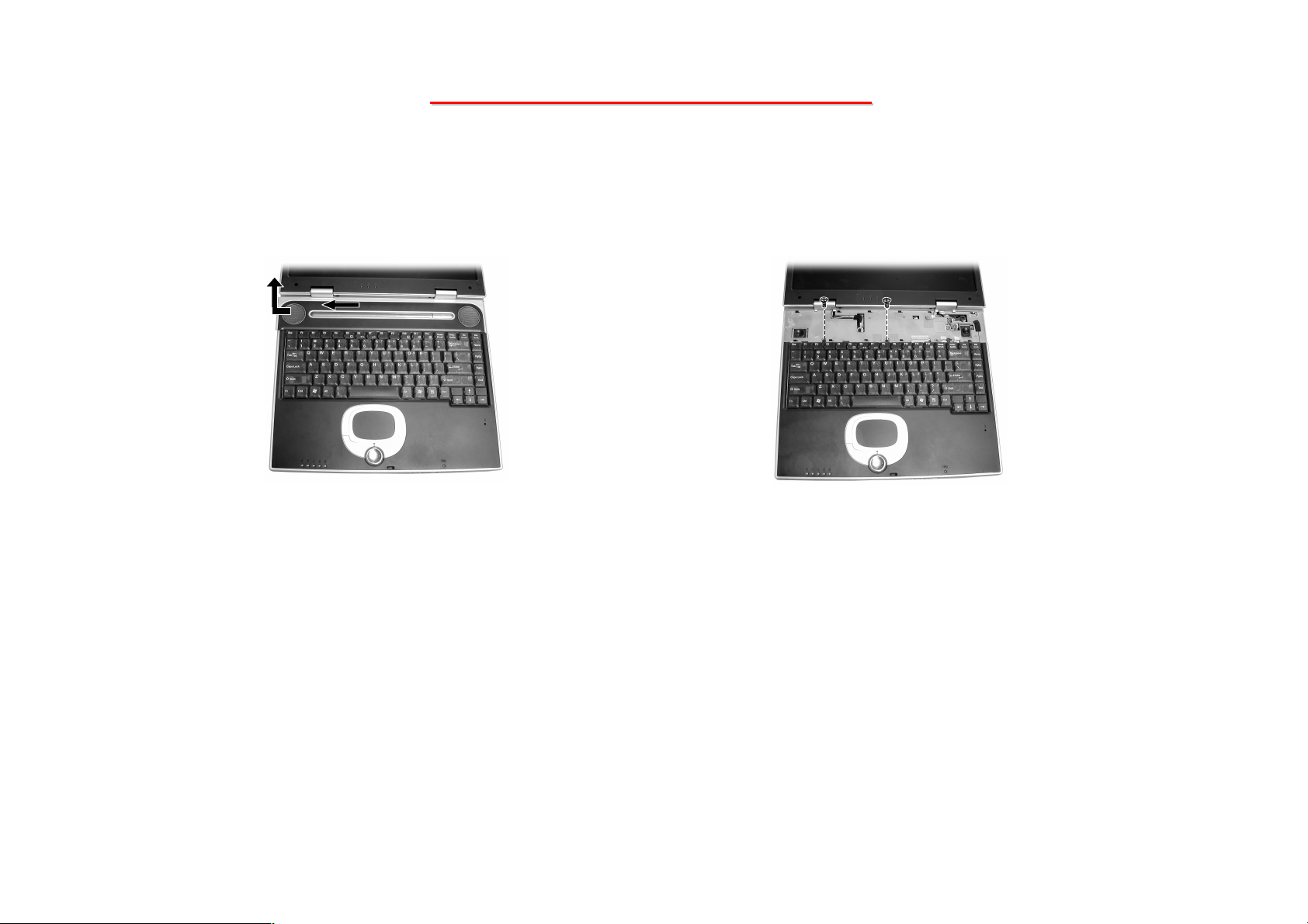
4. Open the top cover. Slide out the keyboard cover. (Figure 2-4)
5. Remove two screws fastening the keyboard. (Figure 2-5)
Figure 2-4 Slide out the keyboard cover Figure 2-4 Remove two screws
73
Page 75
8355 N/B MAINTENANCE
8355 N/B MAINTENANCE
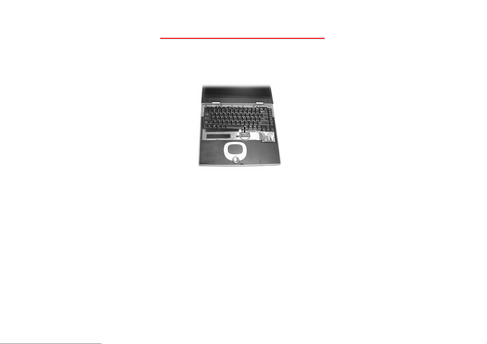
5. Disconnect the cable from system board. (Figure 2-6)
Figure 2-6 Disconnect the cable
Reassembly
1. Reconnect the keyboard cable.
2. Replace the keyboard and secure with two screws.
3. Replace the keyboard cover and secure with three screws.
4. Replace the battery pack. (See section 2.2.1 Reassembly)
74
Page 76
8355 N/B MAINTENANCE
8355 N/B MAINTENANCE
2.2.3 CPU
Disassembly
1. Carefully put the notebook upside down.
2. Remove the battery pack. (See section 2.2.1 Disassembly)
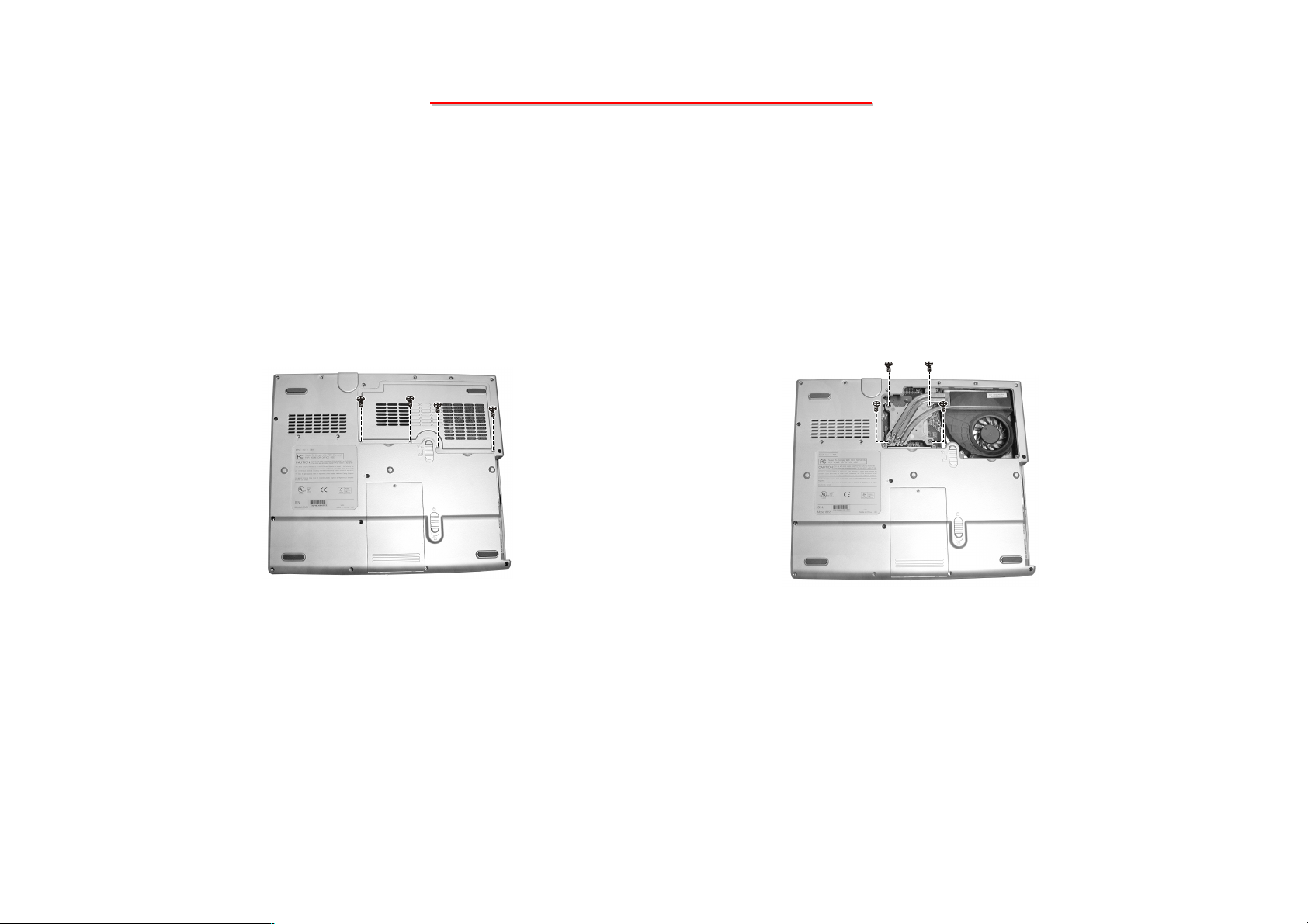
3. Remove four screws that fasten the heatsink compartment covers. (Figure 2-7)
Figure 2-7 Remove four screws
4. Remove four spring screws fastening the heatsink. (Figure 2-8)
Figure 2-8 Remove the heatsink
compartment cover
75
Page 77
8355 N/B MAINTENANCE
8355 N/B MAINTENANCE
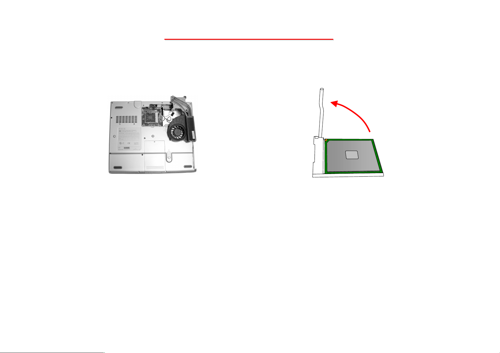
5. Disconnect the fan’s power cord to detach the heatsink from the CPU compartment. (Figure 2-9)
6. To remove the existing CPU, lift the socket arm up to the vertical position. (Figure 2-10)
Figure 2-10 Remove the CPU Figure 2-9 Disconnect the fan’s cord
Reassembly
1. Carefully, align the arrowhead corner of the CPU with the beveled corner of the socket, then insert CPU pins into
the holes. Place the lever back to the horizontal position and push the lever to the left .
2. Connect the fan’s power cord to the system board, fit the heatsink onto the top of the CPU and secure with four
spring screws.
3. Replace the heatsink compartment cover and secure with four screws.
4. Replace the battery pack. (See section 2.2.1 Reassembly)
76
Page 78
8355 N/B MAINTENANCE
8355 N/B MAINTENANCE
2.2.4 HDD Module
Disassembly
1. Carefully put the notebook upside down.
2. Remove the battery pack. (See section 2.2.1 Disassembly)
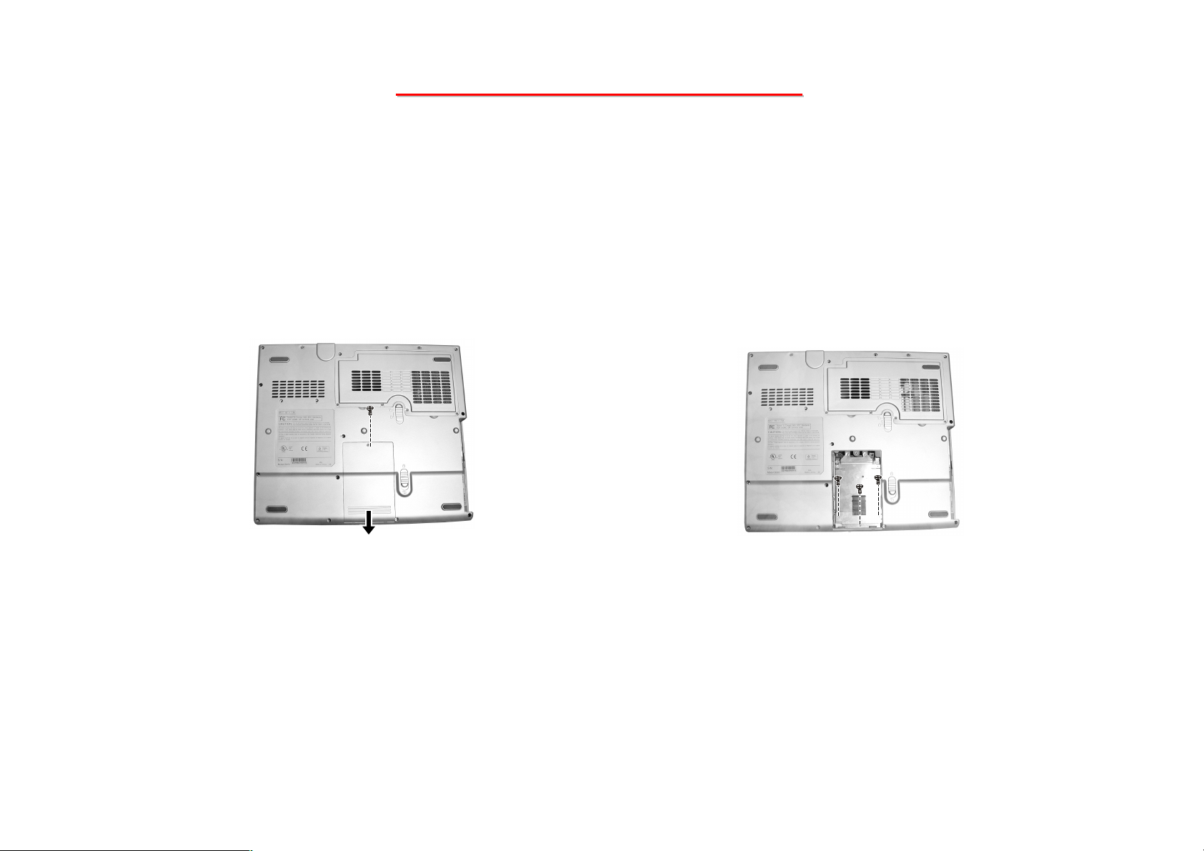
3. Remove one screw fastening the HDD compartment cover. Then sliding it outward. (Figure 2-11)
Figure 2-11 Remove HDD compartment
cover
4. Remove three screws that secure the top shielding of the hard disk drive. (Figure 2-12)
Figure 2-12 Remove three screws that
secure the top shielding
77
Page 79
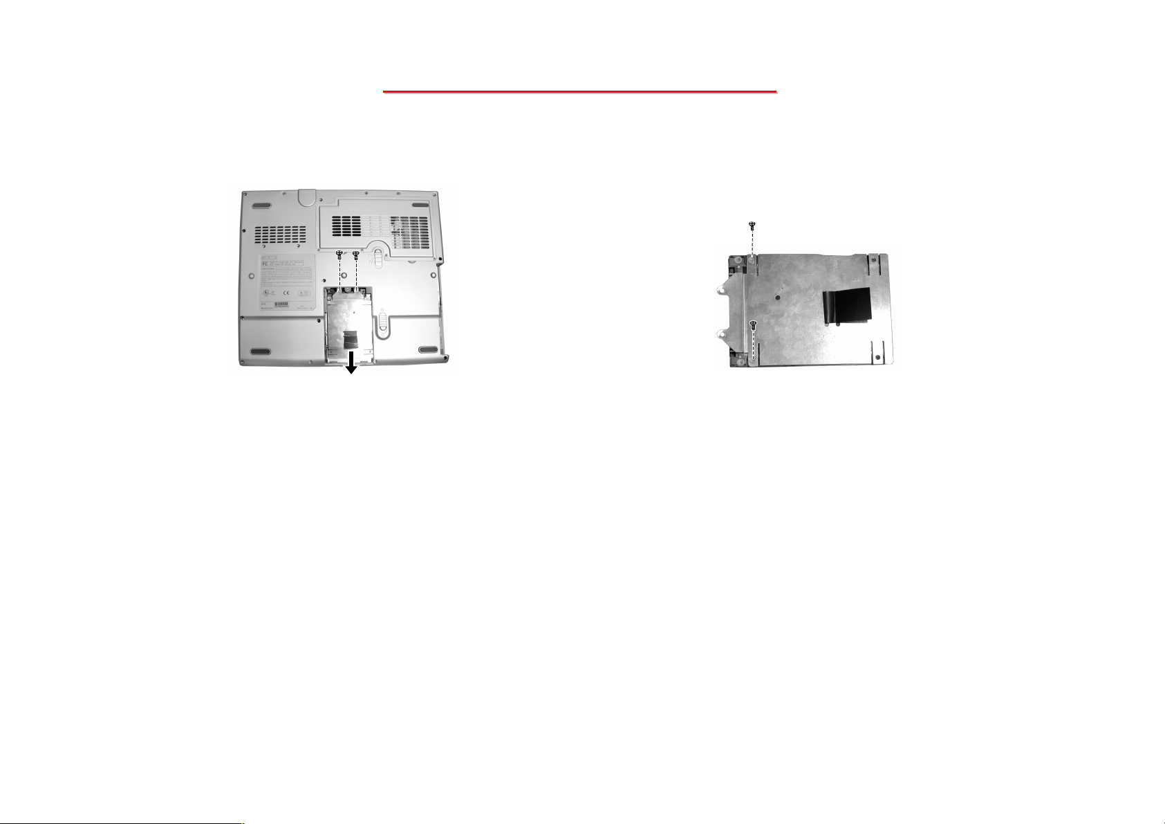
8355 N/B MAINTENANCE
8355 N/B MAINTENANCE
5. Unscrew two screws to slide out the hard disk drive from the compartment. (Figure 2-13)
Figure 2-13 slide out the hard disk drive
6. To free the hard disk drive, remove two screws that secure the holding. (Figure 2-14)
Reassembly
1. Fit the hard disk drive into the holding and secure with two screws.
2. Replace the hard disk drive into compartment and secure with two screws.
3. Fit the top shielding and secure with three screws.
4. Replace the HDD’s cover and secure with one screw.
5. Then replace battery pack. (See section 2.2.1 Reassembly)
Figure 2-14 Free the hard disk
78
Page 80
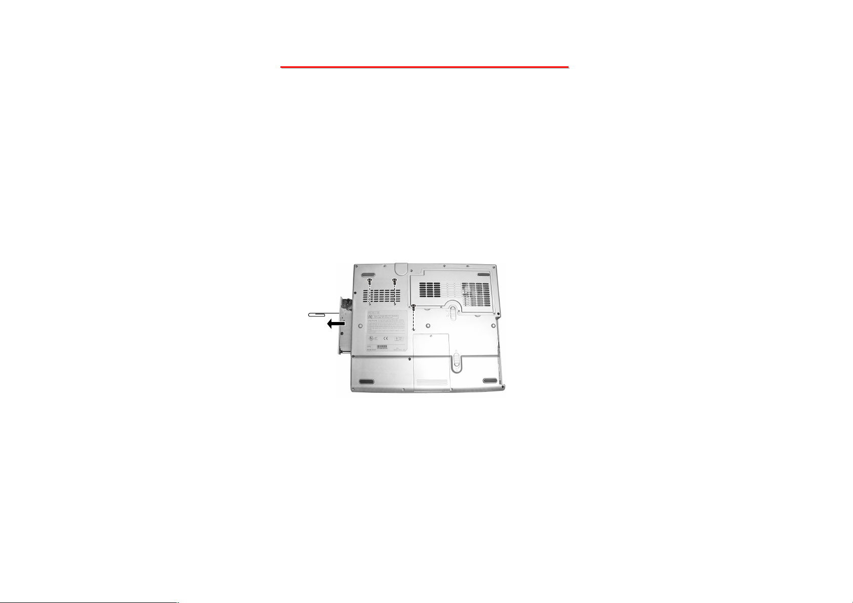
8355 N/B MAINTENANCE
8355 N/B MAINTENANCE
2.2.5 CD/DVD-ROM Drive
DisassemblyDisassembly
1. Carefully put the notebook upside down. Remove the battery pack. (Refer to section 2.2.1 Disassembly)
2. Remove three screws fastening the CD/DVD-ROM drive. (Figure 2-15)
3. Insert a small rod, such as a straightened paper clip, into CD/DVD-ROM drive’s manual eject hole () and push
firmly to release the tray. Then gently pull out the CD/DVD-ROM drive by holding the tray that pops out().
(Figure 2-15)
Figure 2-15 Remove the CD/DVD
-ROM drive
Reassembly
1. Push the CD/DVD-ROM drive into the compartment and secure with three screws.
2. Replace the battery pack. (Refer to section 2.2.1 reassembly)
79
Page 81
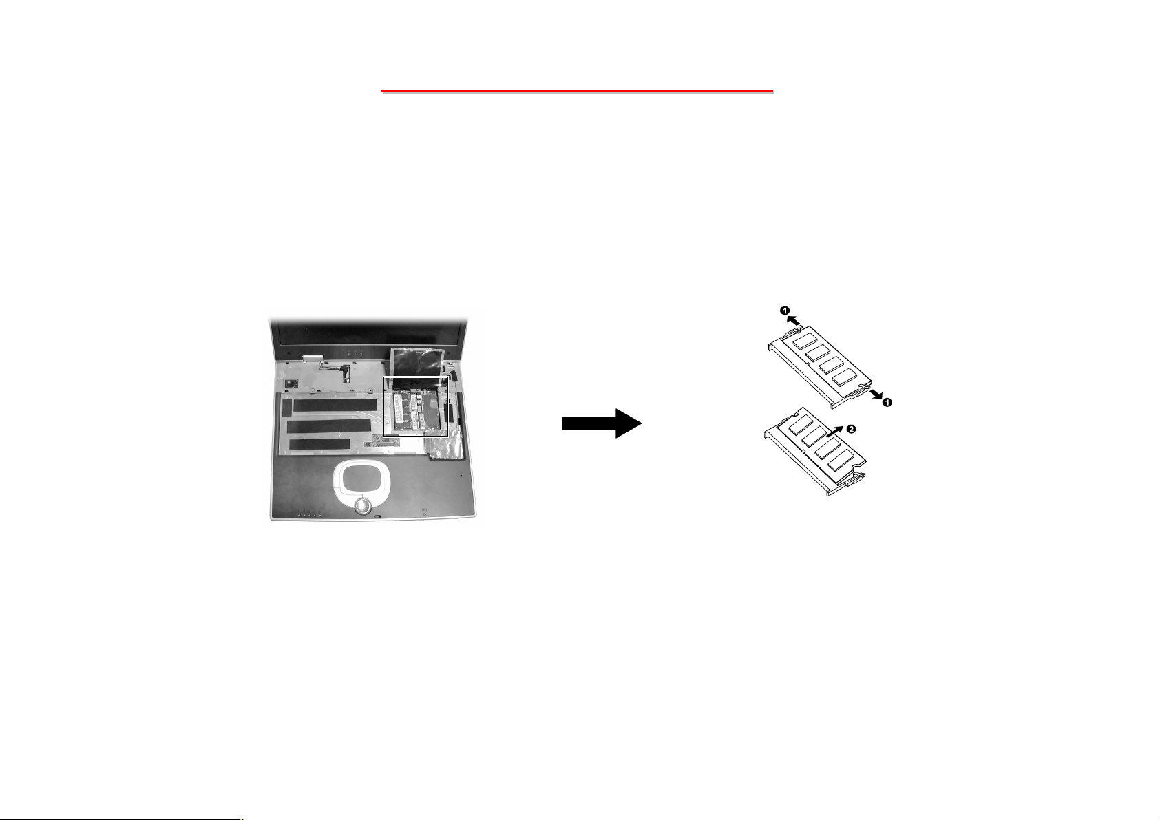
8355 N/B MAINTENANCE
8355 N/B MAINTENANCE
2.2.6 SO-DIMM
Disassembly
1. Carefully put the notebook upside down. And remove the battery pack and the keyboard. (See sections 2.2.1and
2.2.2 disassembly)
2. Pull the retaining clips outwards () and remove the SO-DIMM (). (Figure 2-16)
Figure 2-16 Remove the SO-DIMM
Reassembly
1. To install the DDR, match the DDR's notched part with the socket's projected part and firmly insert the
SO-DIMM into the socket at 20-degree angle. Then push down until the retaining clips lock the DDR into
position.
2. Replace the battery pack and the keyboard. (See sections 2.2.1 and 2.2.2 reassembly)
80
Page 82
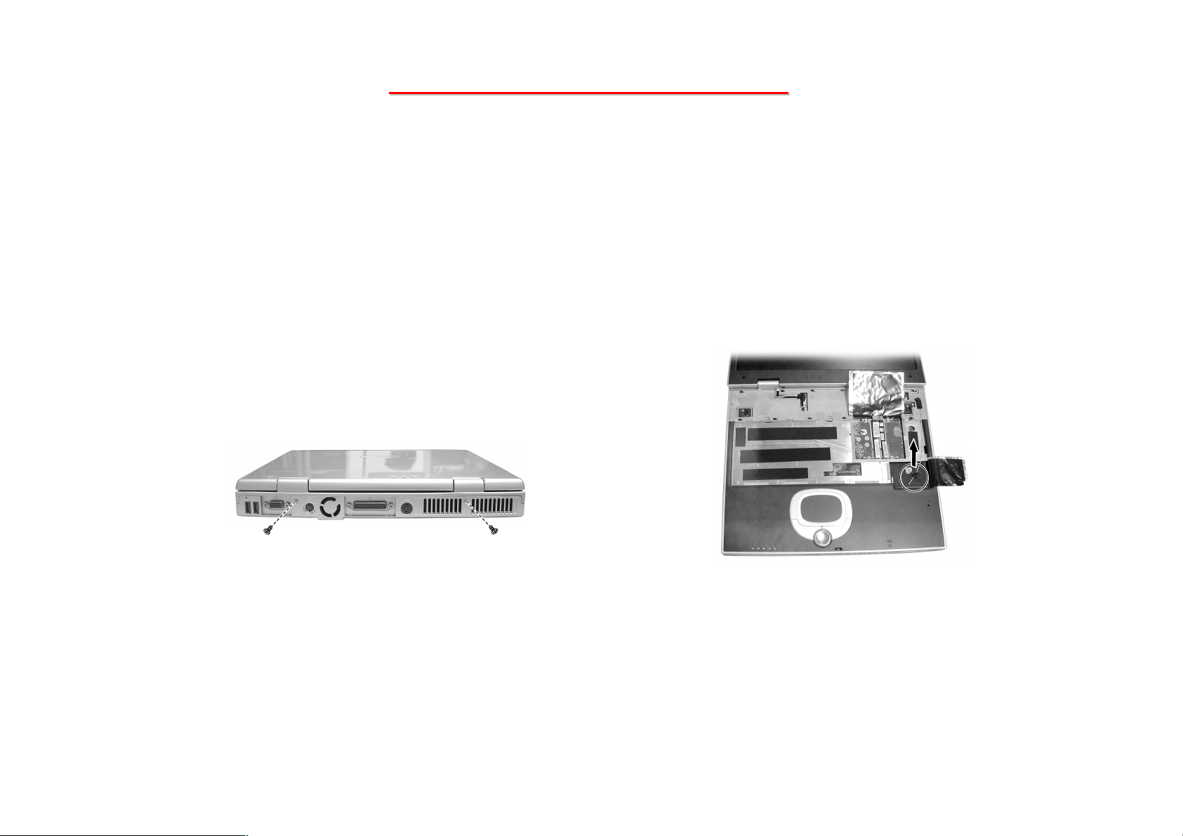
8355 N/B MAINTENANCE
8355 N/B MAINTENANCE
2.2.7 LCD Assembly
Disassembly
1. Carefully put the notebook upside down. And remove the battery pack and the keyboard. (See sections 2.2.1and
2.2.2 disassembly)
2. Remove two screws on the rear side of notebook. (Figure 2-17)
3. Open the top cover. Rip the insulating tape off to free the antenna. (Figure 2-18)
Figure 2-18 Free the antenna Figure 2-17 Remove two screws
81
Page 83
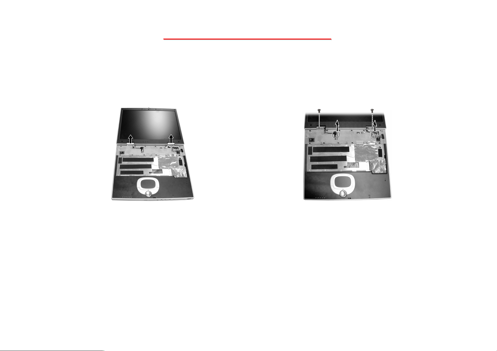
8355 N/B MAINTENANCE
8355 N/B MAINTENANCE
6. Then remove the two hinge covers. (Figure 2-19)
7. Remove two screws of the hinges and disconnect the two LCD wires from the system board. (Figure 2-20)
Figure 2-20 Disconnect the two LCD wiresFigure 2-19 Remove the hinge cover
82
Page 84
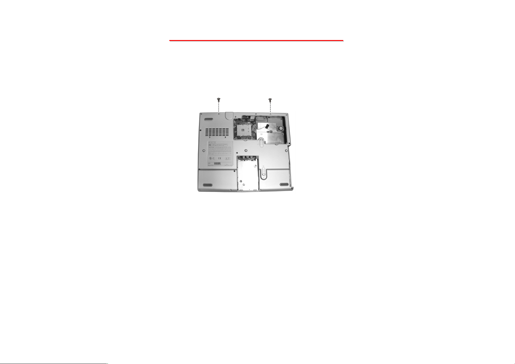
8355 N/B MAINTENANCE
8355 N/B MAINTENANCE
8. Carefully put the notebook upside down,remove two screws of the hinges,Now you can separate the LCD assembly
from the base unit. (Figure 2-21)
Figure 2-21 Remove the LCD assembly
Reassembly
1. Attach the LCD assembly to the base unit and secure with four screws of the hinges.
2. Reconnect the LCD wires to the system board..
3. Fit two hinge covers and secure with two screws.
4. Replace the battery pack and the keyboard. (See section 2.2.1 and 2.2.2 reassembly) .
83
Page 85
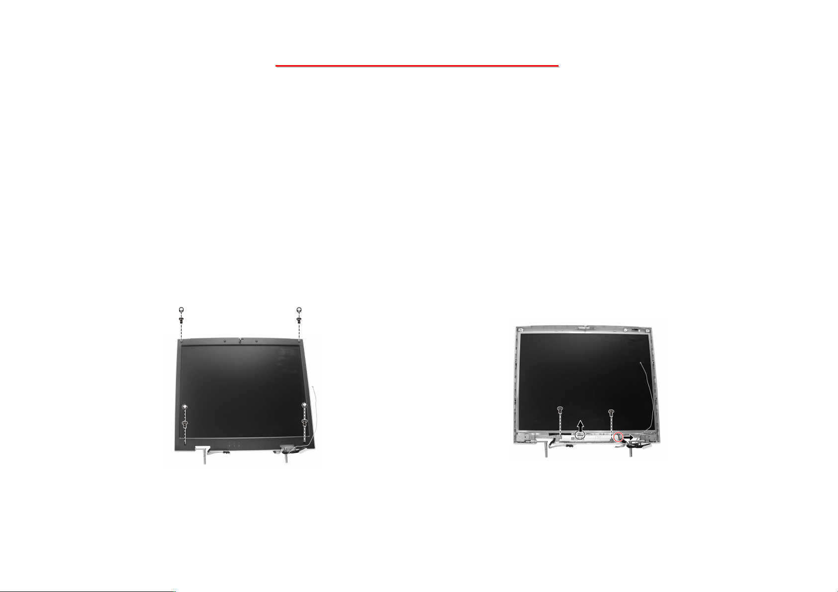
8355 N/B MAINTENANCE
8355 N/B MAINTENANCE
2.2.8 Inverter Board
Disassembly
1. Carefully put the notebook upside down. And remove the battery pack and the keyboard. (See sections 2.2.1and
2.2.2 disassembly)
2. Remove the LCD Assembly. (See section 2.2.7 Disassembly)
3. Remove the four rubber pads and four screws. (figure 2-22)
4. Insert a flat screwdriver to the lower part of the top cover and gently pry the frame out. Repeat the process until the
cover is completely separated from the housing.
5. Disconnect one wire from inverter board and remove two screws fastening the inverter board. (Figure 2-23)
Figure 2-22 Unscrew four screws Figure 2-23 Disconnect one cable
84
Page 86

8355 N/B MAINTENANCE
8355 N/B MAINTENANCE
Reassembly
1. Fit the inverter board back into place and secure with two screws, and reconnect the wire to the inverter board. .
2. Fit the LCD top cover back into the housing and secure with four screws and four rubber pads
3. Replace the LCD Assembly. (See section 2.2.7 Reassembly)
4. Replace the battery pack and the keyboard. (See section 2.2.1 and 2.2.2 reassembly) .
85
Page 87
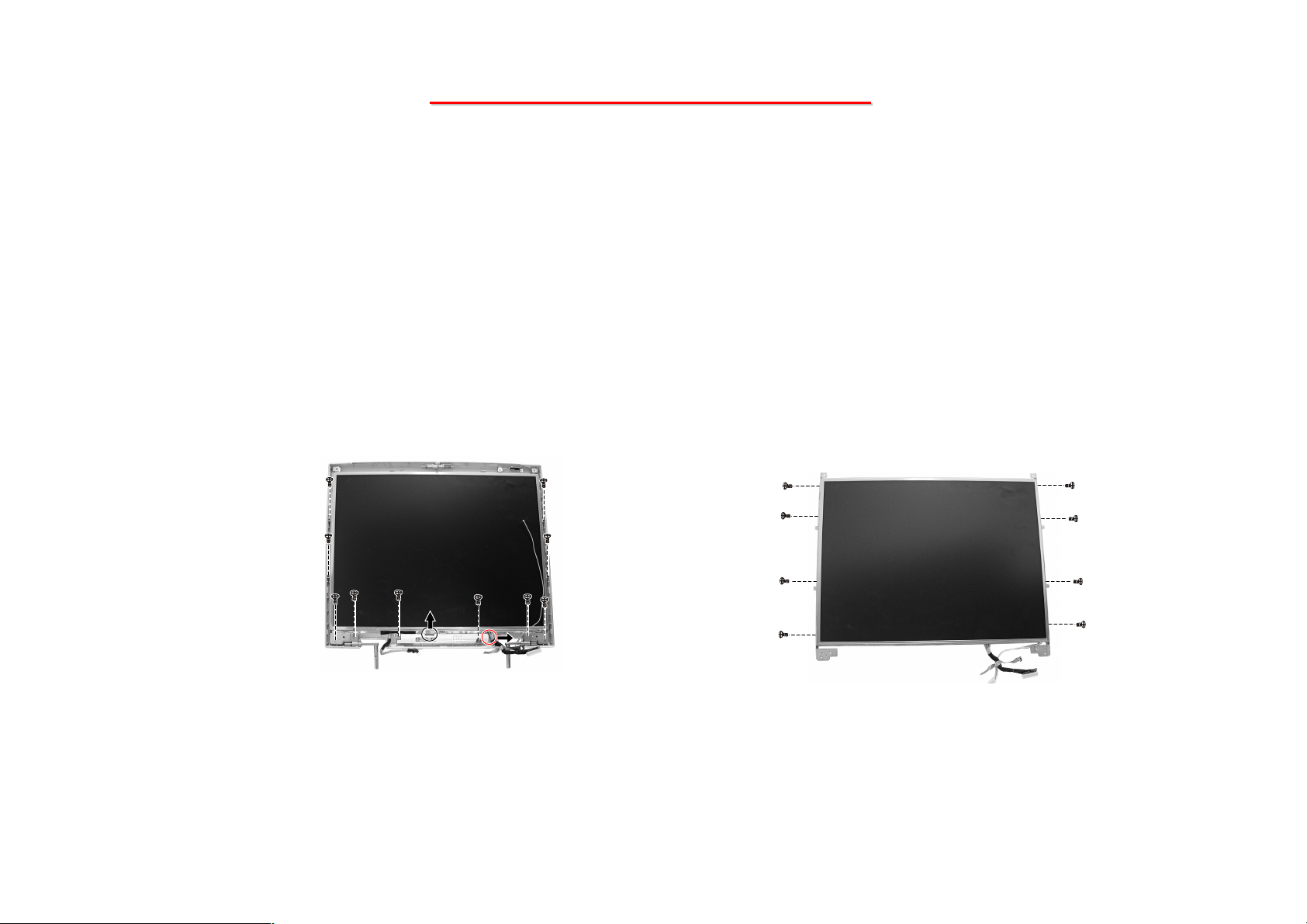
8355 N/B MAINTENANCE
8355 N/B MAINTENANCE
2.2.9 LCD Panel
Disassembly
1. Carefully put the notebook upside down.
2. Remove the battery pack. (See section 2.2.1 Disassembly)
3. Remove the LCD Assembly. (See section 2.2.7 Disassembly)
4. Disconnect one wire from inverter board and remove two screws fastening the inverter board. (Figure 2-22)
5. Remove eight screws. And then lift up LCD panel. (Figure 2-24)
6. To free the LCD panel, remove eight screws. (Figure 2-25)
Figure 2-24 Separate the LCD panel
Figure 2-25 Unscrew eight screws
86
Page 88

8355 N/B MAINTENANCE
8355 N/B MAINTENANCE
Reassembly
1. Attach the LCD panel holding to panel and secure with eight screws.
2. Fit the LCD panel into place and secure with eight screws.
3. Replace the inverter board. (See section 2.2.8 Reassembly)
4. Replace the LCD assembly. (See section 2.2.7 Reassembly)
5. Replace the battery pack. (See section 2.2.1 Reassembly)
87
Page 89
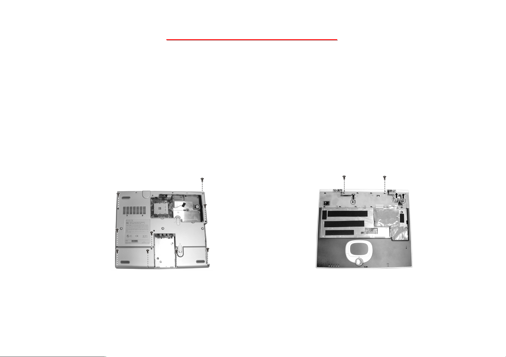
8355 N/B MAINTENANCE
8355 N/B MAINTENANCE
2.2.10 System Board
Disassembly
1. Carefully put the notebook upside down.
2. Remove the battery pack. (See section 2.2.1 Disassembly)
3. Remove the keyboard, CPU, hard disk drive, CD/DVD-ROM drive, DDR-SDRAM and LCD Assembly. (See the
previous sections Disassembly)
4. Remove nine screws on the bottom of notebook. (Figure 2-26)
5. Turnover the notebook. Remove two screws. And disconnect three wires. (Figure 2-27)
Figure 2-27 Remove two screwsFigure 2-26 Unscrew nine screws
88
Page 90
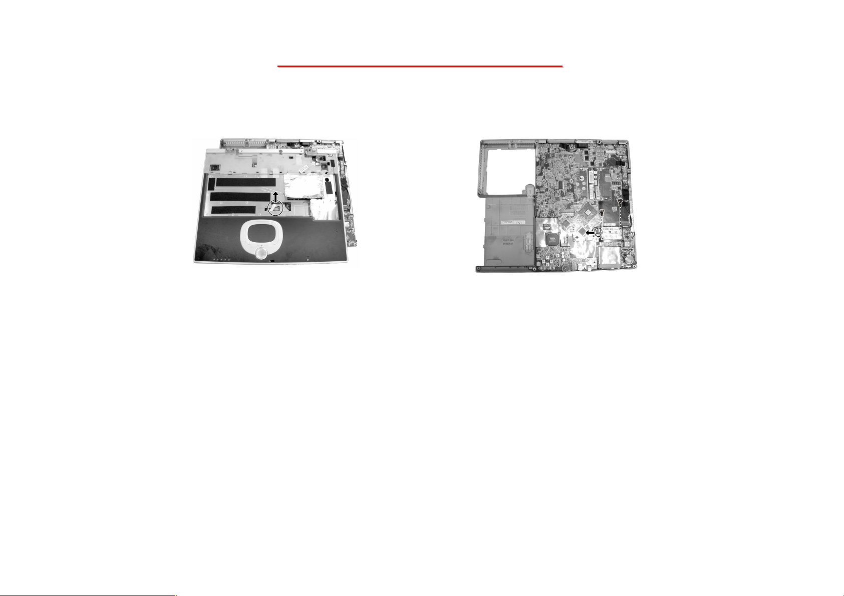
8355 N/B MAINTENANCE
8355 N/B MAINTENANCE
6. Disconnect the touch pad’s cable. Then lift up the system top cover. (Figure 2-28)
Figure 2-28 Remove the top cover
7. To remove the modem card, remove two screws and disconnect the wire. (Figure 2-29)
Figure 2-29 Remove the modem card
89
Page 91
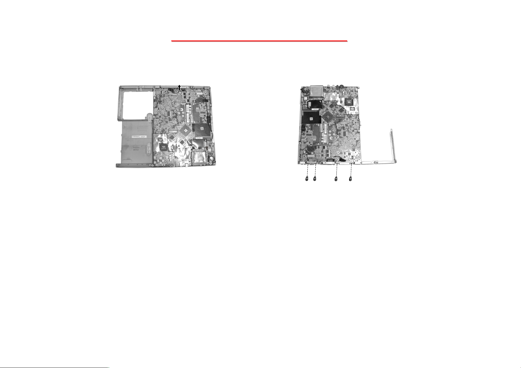
8355 N/B MAINTENANCE
8355 N/B MAINTENANCE
8. Unscrew one screw and disconnect fan’s cord. (Figure 2-30)
Figure 2-30 Unscrew one screw
and disconnect one cord
Figure 2-31 Remove four hex nuts
9. Remove four hex nuts beside the VGA port. Now you can lift up system board from housing.
(Figure 2-31)
90
Page 92

8355 N/B MAINTENANCE
8355 N/B MAINTENANCE
Reassembly
1. Fit the system board back into housing and secure with one screw and four hex nuts.
2. Reconnect the fan’s cord.
3. Reconnect the modem card’s wire. Fit the modem card and secure with two screws.
4. Fit the top cover. Reconnect the touch pad’s cable to system board.
5. Reconnect the speaker’s cords to system board.
6. Fasten the top cover by two screws.
7. Put up the notebook upside down. Reconnect the other speaker’s cord.
8. Fasten the housing by nine screws.
9. Reassemble the notebook. (See the previous sections Reassembly)
91
Page 93
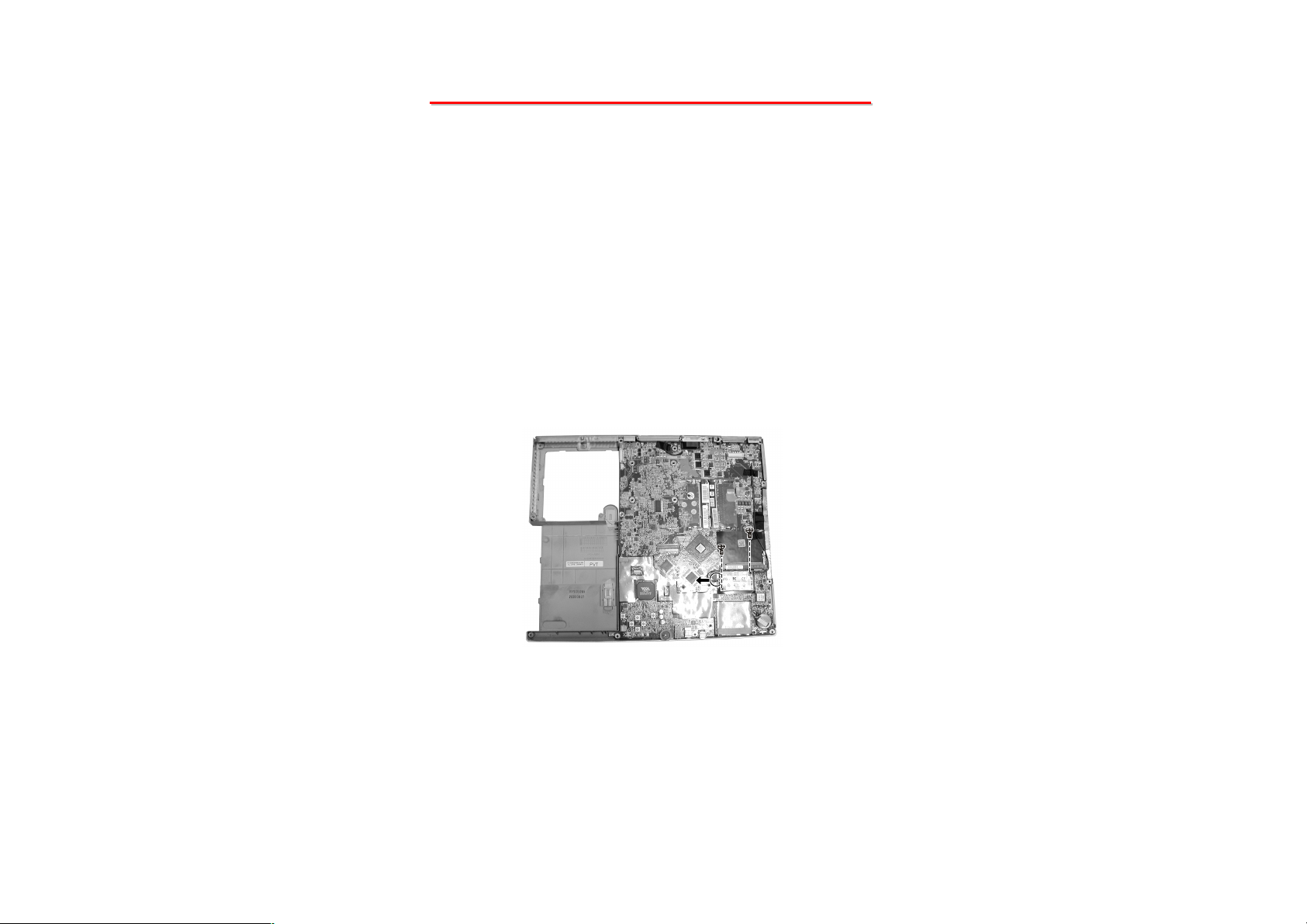
8355 N/B MAINTENANCE
8355 N/B MAINTENANCE
2.2.11 Modem Card
Disassembly
1. Carefully put the notebook upside down.
2. Remove the battery pack. (See section 2.2.1 Disassembly)
3. Remove the keyboard, CPU, hard disk drive, CD/DVD-ROM drive, DDR-SDRAM and LCD Assembly. (See the
previous sections Disassembly)
4. Remove the system top cover. (See the steps1 to 6 of section 2.2.10 Disassembly)
5. Remove two screws fastening the modem card. disconnect cord from system board. (Figure 2-32)
Figure 2-32 Remove the modem card
Reassembly
1. Reconnect the cord. Then fit the modem card and secure with two screws.
2. Reassemble the notebook. (See the previous sections Reassembly)
92
Page 94
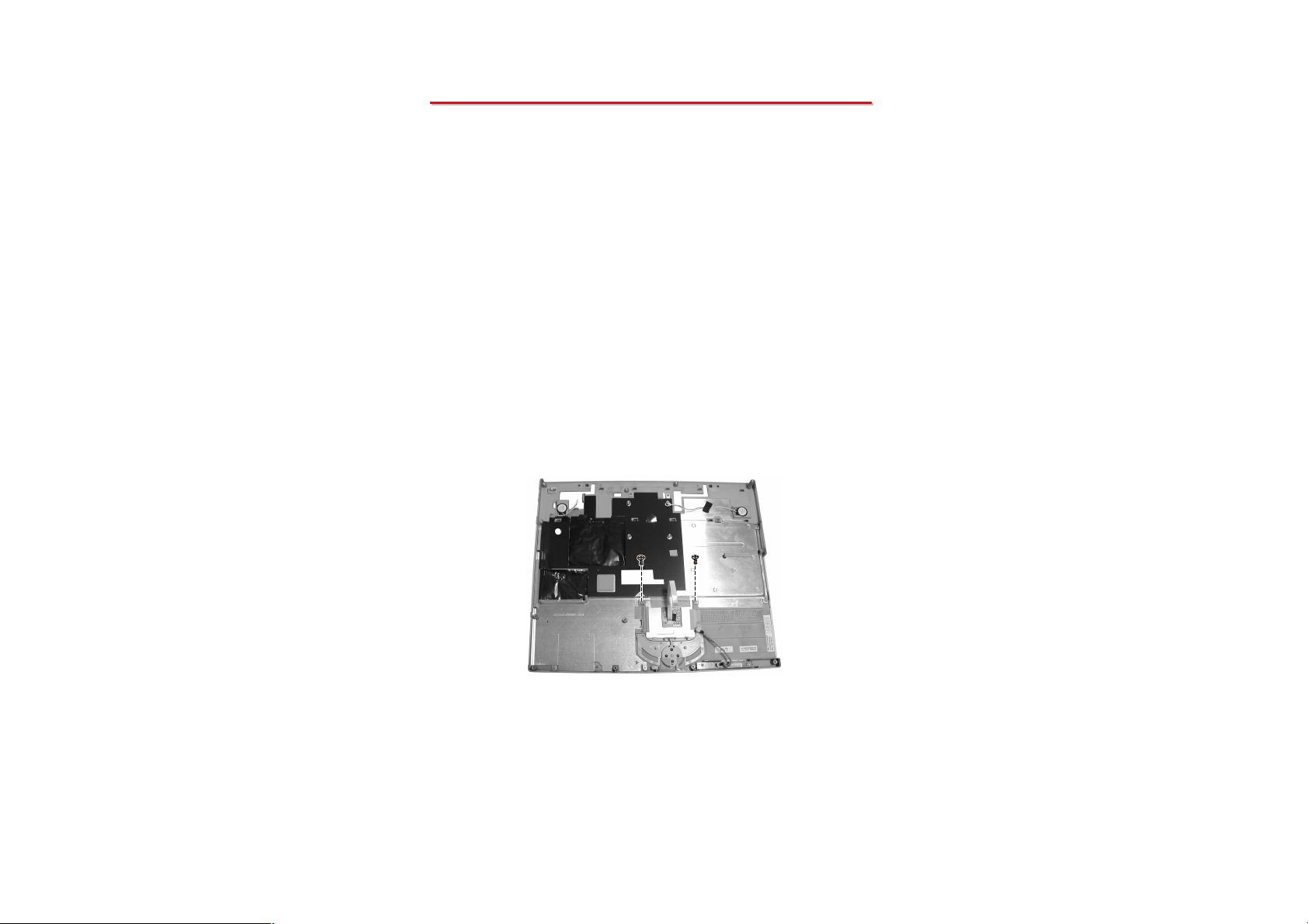
8355 N/B MAINTENANCE
8355 N/B MAINTENANCE
2.2.12 Touch Pad
Disassembly
1. Carefully put the notebook upside down.
2. Remove the battery pack. (See section 2.2.1 Disassembly)
3. Remove the keyboard, CPU, hard disk drive, CD/DVD-ROM drive, DDR-SDRAM and LCD Assembly. (See the
previous sections Disassembly)
4. Remove the system top cover. (See the steps1 to 6 of section 2.2.10 Disassembly)
5. Remove two screws fastening the touch pad bracket. Then remove it. (Figure 2-33)
6. Remove the click holder and touch pad panel. (Figure 2-33)
Figure 2-33 Free the touch pad
93
Page 95

8355 N/B MAINTENANCE
8355 N/B MAINTENANCE
Reassembly
1. Fit the touch pad panel and click holder
2. Then fit the touch pad bracket and secure with two screws.
3. Reassemble the notebook. (See the previous sections Reassembly)
94
Page 96
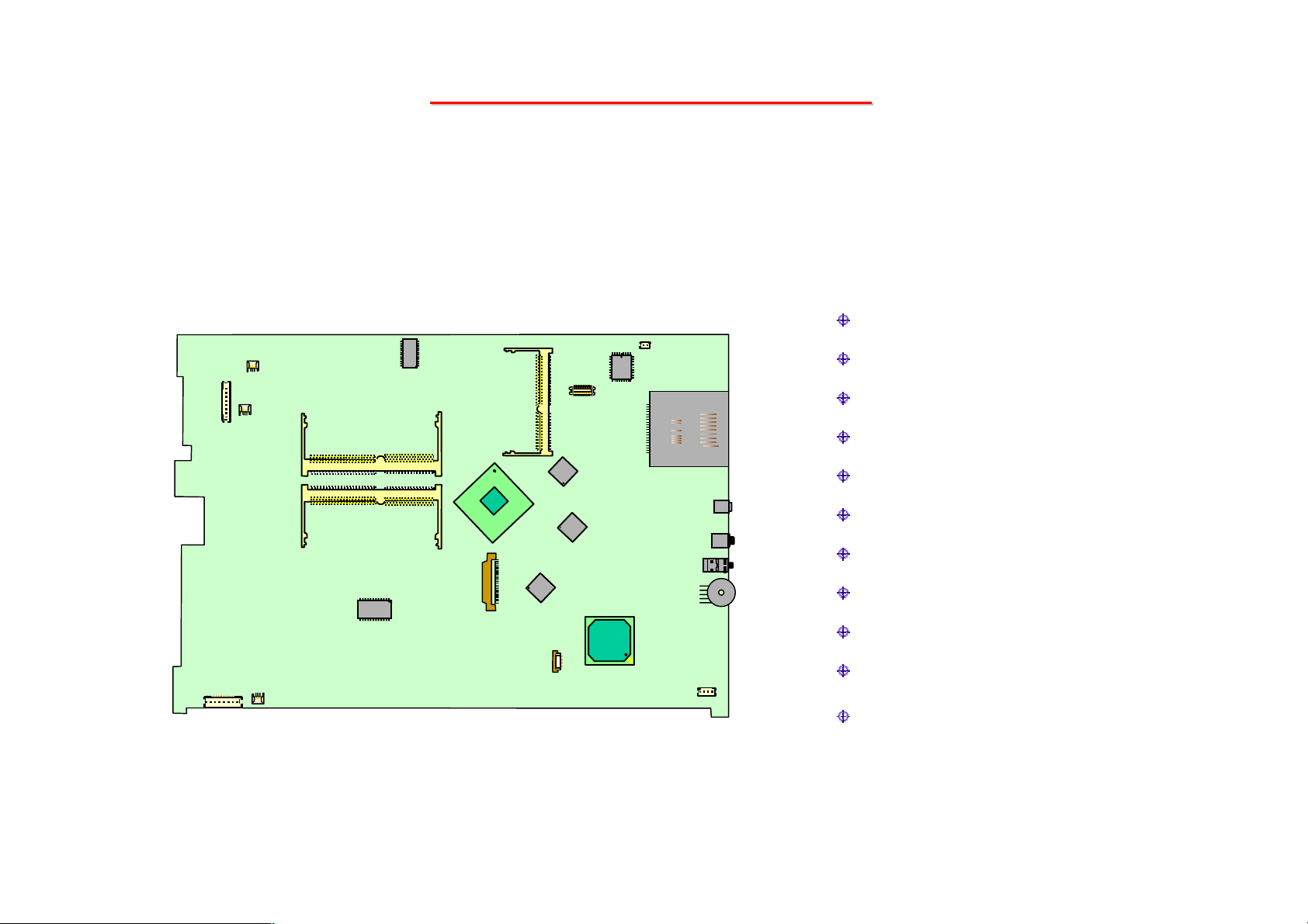
8355 N/B MAINTENANCE
8355 N/B MAINTENANCE
3. Definition & Location of Connectors / Switches
3.1 Main Board (Side A) – 1
J14
J11
J2
J4
J7
J9
J13
J2,J3 : LCD Connector
J4 : Right Internal Speaker Connector
J5 : Left Internal Speaker Connector
J6-7 : DDR SO-DIMM Module Socket
J8 : Internal Keyboard Connector
J6
J8
J10
J5
J3
J15
J9 : Mini PCI Socket
J10 : Touch-pad Connector
J11 : MDC Connector
J13 : Card Reader Connector
J14 : RTC Battery Connector
J15 : LED Indicator Board Connector
------ To next page ------
95
Page 97
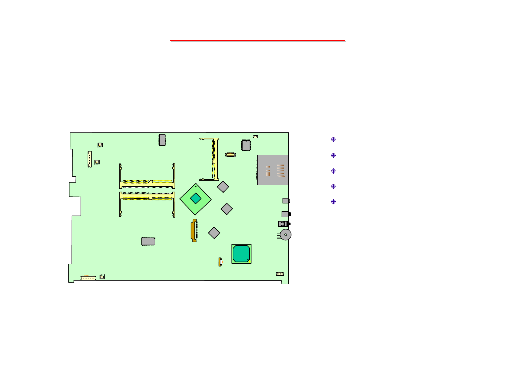
8355 N/B MAINTENANCE
8355 N/B MAINTENANCE
3. Definition & Location of Connectors/ Switches
3.1 Main Board (Side A) – 2
------ Continued to previous page ------
J19
J17
VR1
J16
J18
J16 : IEEE1394 Connector
J17 : External Audio Output
J18 : External Microphone Input
J19 : MDC Jump Wire Connector
VR1 : Volume Controller
96
Page 98
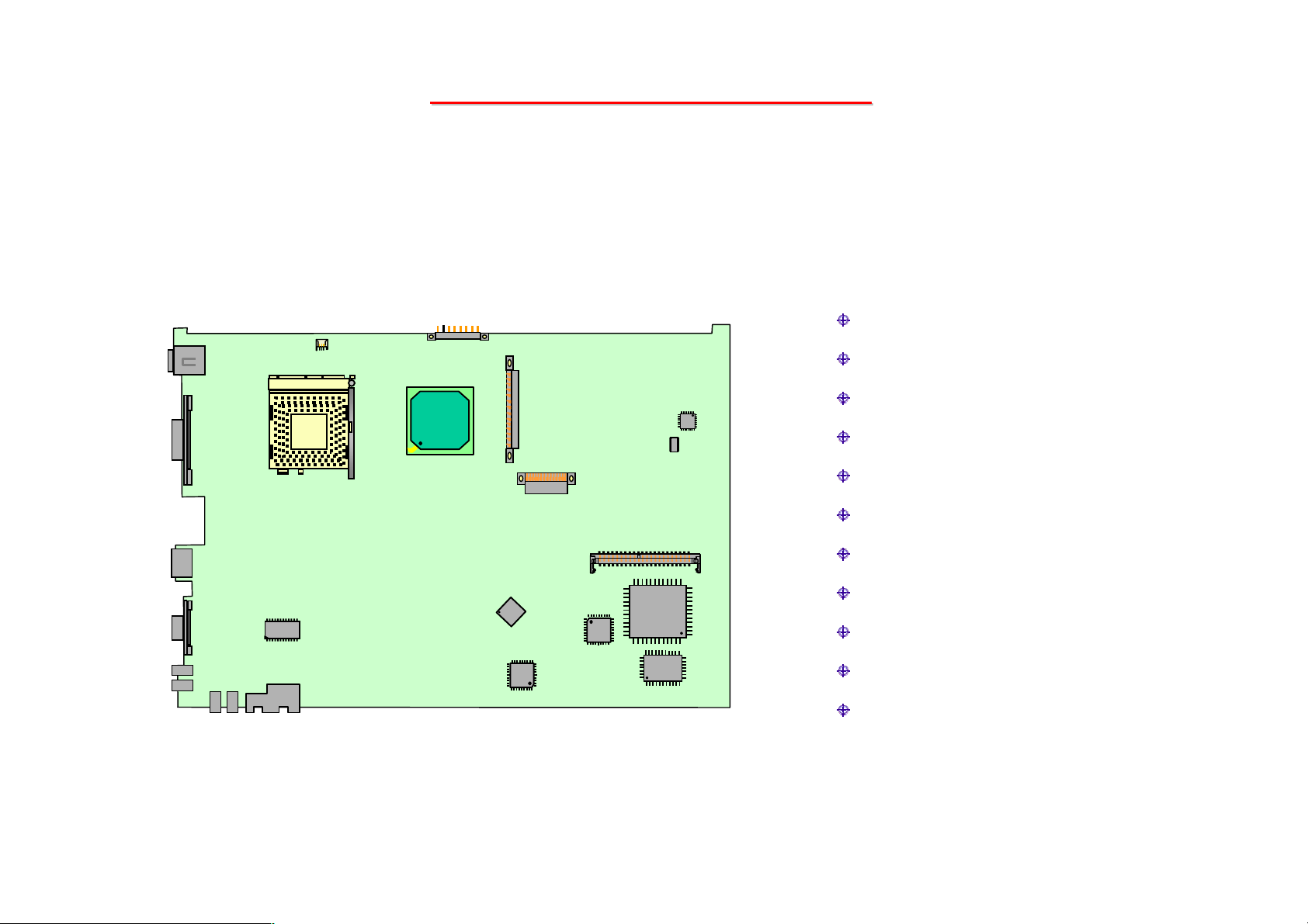
8355 N/B MAINTENANCE
8355 N/B MAINTENANCE
3. Definition & Location of Connectors/ Switches
3.1 Main Board (Side B)
J528
PJ501
PJ502
PJ501 : AC Power Jack
PJ502 : Battery Connector
J521
J522
J502
J501
J503
J523
J524
J527
J529
J530
J501 : S-Video Connector
J502 : Parallel Port Connector
J503 : CRT Connector
J521-524 : USB Ports Connector
J532
J527 : RJ45/RJ11 Connector
J528 : FAN Connector
J529 : HDD Connector
J530 : CDROM Connector
J532 : PCMCIA Card Bus Socket
97
Page 99
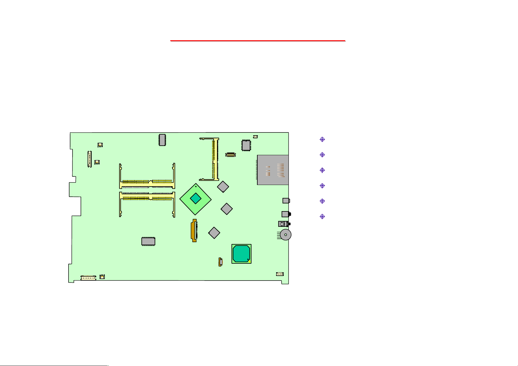
8355 N/B MAINTENANCE
8355 N/B MAINTENANCE
4. Definition & Location of Major Components
4.1 Main Board (Side A)
U9
U12
U16
U18
U30
U29
U23
U9 : ICS950403 Clock Generator
U12 : VT6103 LAN Controller
U16 : VGA Control Chip ATI M10
U18,U29,U30 : On Board External VRAM
U20 : South Bridge VT8235
U23 : Flash ROM (BIOS)
U20
98
Page 100
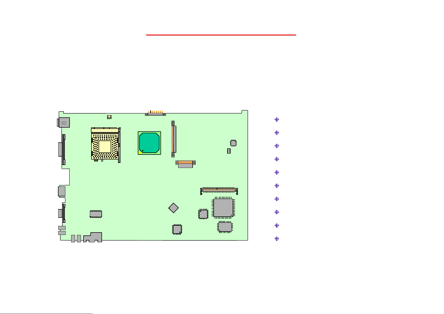
8355 N/B MAINTENANCE
8355 N/B MAINTENANCE
4. Definition & Location of Major Components
4.1 Main Board (Side B)
U503 : CPU Socket
PU502
U503
U506
U523
U509
U511
U517
U518
U516
U506 : North Bridge VT8385
U509 : PC87393 Super I/O Controller
U511 : H8/F3437 Micro Controller
U514 : ENE CP710 PCMCIA &Reader Controller
U516 : VT6307L IEEE1394 Controller
U517 :TPA0202 Audio Amplifier
U514
U518 : CMI9738 Audio CODEC
U523 : On Board External VRAM
PU502 :CPU Power Controller
99
 Loading...