

Page 1

SERVICE MANUAL FOR
SERVICE MANUAL FOR
SERVICE MANUAL FOR
8599
8599
85998599
8599
8599
85998599
8599
8599
85998599
BY:
Repair Technology Research Department /EDVD
Repair Technology Research Department /EDVD
Star
Star
Jun.2004
Meng
Meng
Page 2
Contents
8599
8599
N/B Maintenance
N/B Maintenance
1. Hardware Engineering Specification ………………………………………………………………………
1.1 Introduction ………………………………………………………………………………………………………………..
1.2 Hardware System…………………………………………………………………………………………………………..
1.3 Electrical Characteristic ………………………………………………………………………………………………….
1.4 Appendix 1 : SiS963L GPIO Definition ………………………………………………………………………………….
1.5 Appendix 2 : Keyboard Controller Pins Definition ……………………………………………………………………..
1.6 Appendix 3: Audio Performance …………………………………………………………………………………………
2. System View and Disassembly ……………………………………………………………………………..
2.1 System View ……………………………………………………………………………………………………………….
2.2 System Disassembly ……………………………………………………………………………………………………….
3. Definition & Location of Connectors / Switches …………………………………………………………..
3.1 Mother Board ……………………………………………………………………………………………………………...
4. Definition & Location of Major Components ……………………………………………………………..
4
4
7
37
42
43
45
46
46
49
69
69
72
4.1 Mother Board ……………………………………………………………………………………………………………...
5. Pin Description of Major Component …….……………………………………………………………….
5.1 Inter Pentium 4 Processor mFC-PGA 478 Pins …………………………………………………………………………
5.2 SiS M661FX (IGUI Host Memory Controller) …………………………………………………………………………
5.3 SiS963L (MuTIOL®Media I/O South Bridge) ………………………………………………………………………….
72
73
73
78
83
1
Page 3
Contents
8599
8599
N/B Maintenance
N/B Maintenance
6. System Block Diagram ……………………………………………………………………………………..
7. Maintenance Diagnostics …………………………………………………………………………………..
7.1 Introduction ……………………………………………………………………………………………………………….
7.2 Error Codes ……………………………………………………………………………………………………………….
7.3 Debug Tool …………………………………………………………………………………………………………………
8. Trouble Shooting ……………………………………………………………………………………………
8.1 No Power …………………………………………………………………………………………………………………..
8.2 Battery Can not Be Charged ……………………………………………………………………………………………..
8.3 No Display …………………………………………………………………………………………………………………
8.4 LCD No Display or Picture Abnormal …………………………………………………………………………………..
8.5 External Monitor No Display or Color Abnormal ………………………………………………………………………
8.6 TV Test Error ……………………………………………………………………………………………………………..
8.7 Memory Test Error ……………………………………………………………………………………………………….
8.8 Keyboard (K/B) Touch-Pad (T/P) Test Error …………………………………………………………………………..
8.9 Hard Driver Test Error …………………………………………………………………………………………………..
8.10 CD-ROM Driver Test Error …………………………………………………………………………………………….
8.11 USB Port Test Error …………………………………………………………………………………………………….
8.12 PC Card Socket Test Error ……………………………………………………………………………………………..
8.13 Mini-PCI Socket Test Error …………………………………………………………………………………………..
8.14 Audio Failure …………………………………………………………………………………………………………….
89
90
90
91
93
94
96
99
101
105
107
109
111
113
115
117
119
123
125
127
2
Page 4
Contents
8599
8599
N/B Maintenance
N/B Maintenance
8.15 LAN Test Error ………….………………………………………………………………………………………………
9. Spare Parts List ……………………………………………………………………………… …………….
10. System Exploded Views …………………………………………………………………………………..
11. Circuit Diagram …………………………………………………………………………………………..
12. Reference Material ………………………………………………………………………………………..
130
132
143
144
172
3
Page 5
8599
8599
N/B Maintenance
N/B Maintenance
1. Hardware Engineering Specification
1.1 Introduction
1.1.1 General Description
This document describes the system hardware engineer specification for 8599 portable notebook computer system.The
8599 notebook computer is a new mainstream high performance easy assembly notebook in the MiTAC notebook
family.
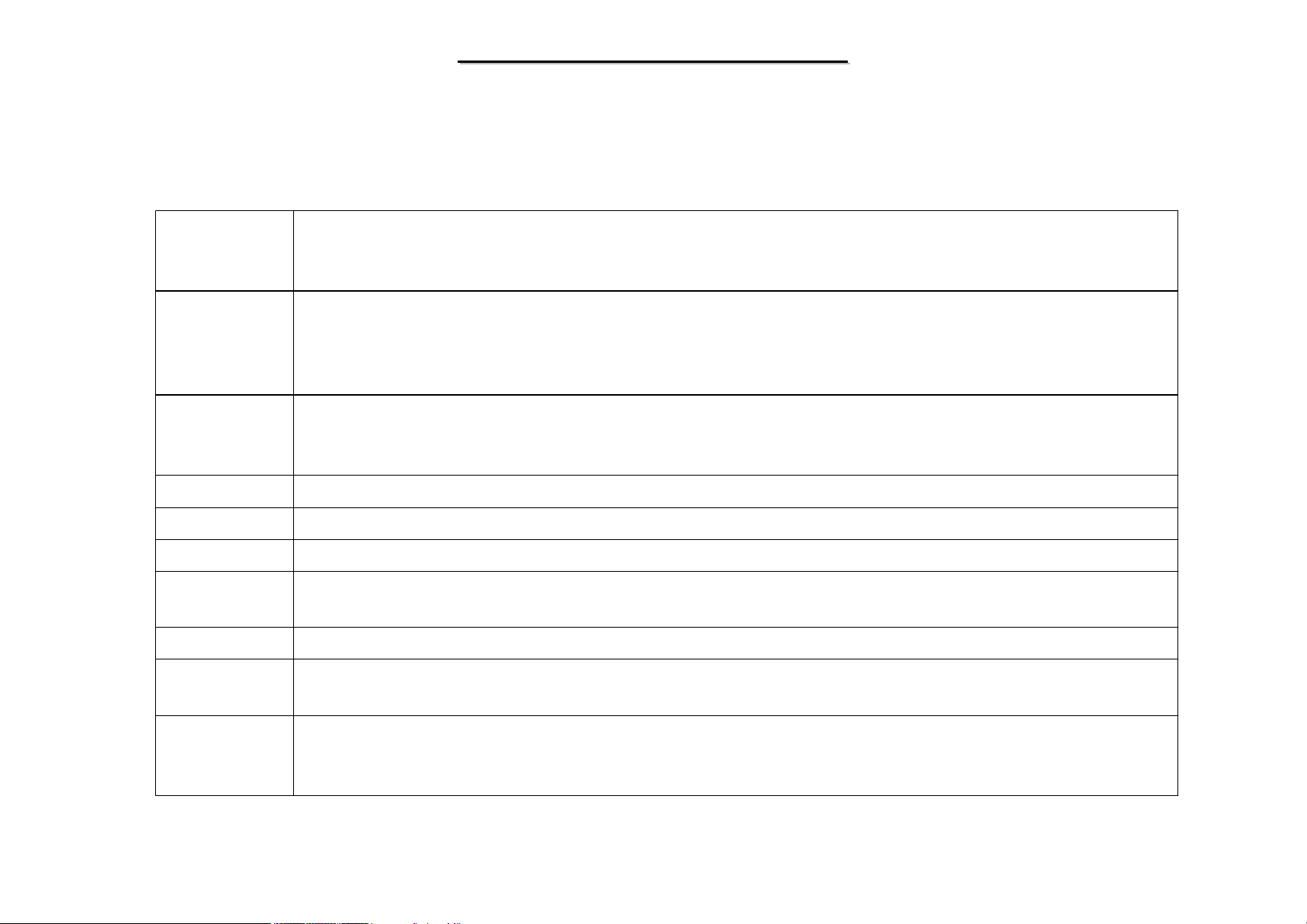
1.1.2 System Overview (1)
Table 1. Hardware Specification
CPU
Core logic
L2 Cache
System BIOS
- Intel DT NW P4 2.4G,2.5G,2.53G,2.6G,2.66G,2.8G,3.06Ghz(p) w/z HT - FSB 800/533 MHz
- Intel DT NW Celeron 2.0G~2.8G w/z - FSB 400MHz
- Intel DT Prescott Celeron 2.4G,2.53G,2.66G,2.8G,3.06G,3.2G w/z - FSB 533MHz
- Intel Northwood Mobile P4 2.40G,2.66G,2.80G,3.06G
- Thermal ceiling 81.8W
- SiS M661FX + SiS963L
- 512KB OD for N/W DT & Mobile P4,128KB for N/W Celeron,256KB for Prescott Celeron
-Insyde 256KB(P) Flash EPROM (Include System BIOS and VGA BIOS)
-ACPI 1.0b;DMI 2.3.1 compliant
-Plug & Play capability
4
Page 6
8599
8599
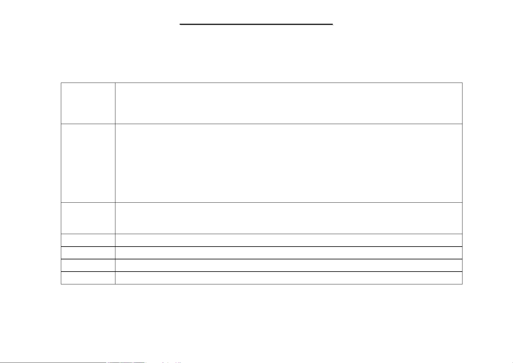
1.1.2 System Overview (2)
Continue to the previous page
N/B Maintenance
N/B Maintenance
Memory
ROM Drive
HDD
Keyboard
PCMCIA
- 0MB on board;Expandable up to 1024MB
- Expandable with combination of optional 128MB/256MB/512MB memory
- 184-pin DDR 266/333/400 DROM Memory Module x 2
- 12.7mm Height
- CD/DVD ROM Drive
- Combo Drive
- Super Combo Drive
- 2.5” 8.45/9.5 mm height:10/15/20/40GB
- Support Ultra-DMA 66/100 function
- User removable by latch,design reserve for screw fix
- Support External FDD w/z USB 1/F; 3.5” Format for 720KB/1.2MB/1.44MBExt.FDD
- 15” XGA/TFT display; Resolution:1024x768Display
- SiS M661FX Int. w/64MB SMAVideo Controller
- 19mm key pitch/ 3.0mm key stroke/ 307mm length
- Windows Logo Key x 1; Application Key x 1
- Glide pad with 2x buttons and direction Scroll buttonPointing Device
- Type II x 1 without ZV
- Cardbus Support
Indictor
- 3 LEDs for Power/battery/charge status (on display Housing/cover)
- 1 LEDs for Radio wave status Power LED (BTO: Wireless LAN only)
- 5 LEDs for HDD Access,ODD Access, Num lock, Cap lock and Scroll Lock
5
Page 7
8599
8599
1.1.2 System Overview (3)
Continue to the previous page
N/B Maintenance
N/B Maintenance
Audio System
I/O Port
Communication
Battery
- Sound Blaster Pro compatible
- Built-in mono microphone
- AC97 2.2 Codec
- 2X 2W Speakers
- USB port (2.0, backward compatible with USB 1.1) x 6
- RJ-11 port x 1
- RJ-45 port x 1
- DC input x 1
- VGA monitor port x 1
- Audio-out x 1
- Mic-in x 1
- S-Video TV-Out x 1 (NTSC/PAL)
- Built-in 56Kbps V.90 modem
- Built-in 10/100 based-T LAN
- One Mini-PCI slot and antenna reserved for wireless LAN
- 8 cell (2000mAH/3.7V) Li-ION smart battery
- Universal AC adapter 90W(P); Input: 100-240V,50/60hZ AC (support power on charge)AC adapter
- 332x285x42 (max) (P)Dimensions
- 3.5kg (P)Weight
6
Page 8

8599
8599
N/B Maintenance
N/B Maintenance
1.2 Hardware System
1.2.1 CPU Module
The Intel®Northwood DT Pentium®4 processor, Intel’s most advanced, most powerful processor, is based on the
new Intel®NetBurst™micro-architecture. The Pentium 4 processor is designed to deliver performance across
applications and usages where end users can truly appreciate and experience the performance. These applications
include Internet audio and streaming video,image processing, video content creation, speech, 3D, CAD, games,
multi-media, and multi-tasking user environments. The Intel Northwood DT Pentium 4processor delivers this
world-class performance for consumer enthusiast and business professional DT users as well as for entry-level
workstation users.
Highlights of the Northwood DT Pentium 4 Processor:
Available at speeds ranging from2.26G/2.4G/2.5G/ 2.53G/2.66G/2.8G/3.06G Hz
Featuring the new Intel NetBurst™micro-architecture
Fully compatible with existing Intel Architecture-based software
Internet Streaming SIMD Extensions 2
Intel®MMX™media enhancement technology
Memory cache ability up to 4 GB of addressable memory space and system memory scalability up to 64GB of
physical memory
Support for uni-processor designs
Based upon Intel’s 0.13 micron manufacturing process
7
Page 9

8599
8599
Intel Pentium 4 Processor Product Feature:
The Intel NetBurst™micro-architecture delivers a number of new and innovative features including Hyper
Pipelined Technology, 400 or 533 MHz System Bus, Execution Trace Cache, and Rapid Execution Engine as
well as a number of enhanced features Advanced Transfer Cache, Advanced Dynamic Execution, Enhanced
Floating-point and Multi-media Unit, and Streaming SIMD Extensions 2. Many of these new innovations and
advances were made possible with improvements in processor technology, process technology, and circuit
design that could not previously be implemented in high-volume, manufacturability solutions. The features and
resulting benefits of the new micro-architecture are defined below.
Hyper Pipelined Technology
The hyper-pipelined technology of the NetBurst™micro-architecture doubles the pipeline depth compared to
N/B Maintenance
N/B Maintenance
theP6 micro-architecture used on today’s Pentium III processors. One of the key pipelines, the branch
prediction / recovery pipeline, is implemented in 20 stages in the NetBurst™micro-architecture, compared to 10
stages in the P6 micro-architecture. This technology significantly increases the performance, frequency, and
scalability of the processor.
400/533 MHz System Bus:
The Northwood DT Pentium 4 processor supports Intel’s highest performance desktop system bus by delivering
3.2 or 4.3GBof data per second into and out of the processor. This is accomplished through a physical signaling
scheme of quad pumping the data transfers over a100/133-MHz clocked system bus and a buffering scheme
allowing for sustained 400/533-MHz data transfers. This compares to 1.06 GB/s delivered on the Pentium III
processor’s 133-MHz system bus.
8
Page 10

8599
8599
Level 1 Execution Trace Cache:
In addition to the 8KB data cache, the Pentium 4 processor includes an Execution Trace Cache that stores up
to12K decoded micro-ops in the order of program execution. This increases performance by removing the
decoder from the main execution loop and makes more efficient usage of the cache storage space since
instructions that are branched around are not stored. The result is a means to deliver a high volume of
instructions to the processor’s execution units and a reduction in the overall time required to recover from
branches that have been mis-predicted.
Rapid Execution Engine:
Two Arithmetic Logic Units (ALUs) on the Pentium 4 processor are clocked at twice the core processor
frequency. This allows basic integer instructions such as Add, Subtract, Logical AND,Logical OR, etc. to
N/B Maintenance
N/B Maintenance
execute in half a clock cycle. For example, the Rapid Execution Engine on a 1.50 GHz Pentium 4 processor
runs at 3 GHz.
512KB, Level 2 Advanced Transfer Cache:
The Level 2 Advanced Transfer Cache (ATC) is 512KB in size and delivers a much higher data throughput
channel between the Level 2 cache and the processor core. The Advanced Transfer Cache consists of a 256bit(32-byte) interface that transfers data on each core clock. As a result,the Northwood DT Pentium 4 processor
1.6 GHz can deliver a data transfer rate of 48 GB/s.This compares to a transfer rate of 16 GB/s on the Pentium
III processor at 1 GHz. Features of the ATC include:
Non-Blocking, full speed, on-die Level 2 cache
8-way set associativity
9
Page 11

8599
8599
256-bit data bus to the level 2 cache
Data clocked into and out of the cache every clock cycle
Advanced Dynamic Execution:
The Advanced Dynamic Execution engine is a very deep, out-of-order speculative execution engine that keeps
the execution units executing instructions. The Pentium 4 processor can also view 126 instructions in flight and
handle up to 48 loads and 24 stores in the pipeline. It also includes an enhanced branch prediction algorithm
that has the net effect of reducing the number of branch mis-predictions by about 33% over the P6 generation
processor’s branch prediction capability. It does this by implementing a 4KB branch target buffer that stores
more detail on the history of past branches, as well as by implementing a more advanced branch prediction
algorithm.
N/B Maintenance
N/B Maintenance
Enhanced Floating-Point and Multimedia Unit:
The Pentium 4 processor expands the floating-point registers to a full 128-bit and adds an additional register
for data movement which improves performance on both floating-point and multimedia applications..
Internet Streaming SIMD Extensions 2 (SSE2):
With the introduction of SSE2, the NetBurst™micro-architecture now extends the SIMD capabilities that MMX
technology and SSE technology delivered by adding 144 new instructions. These instructions include 128-bit
SIMD integer arithmetic and 128-bit SIMD double-precision floating-point operations. These new instructions
reduce the overall number of instructions required to execute a particular program task and as a result can
contribute to an overall performance increase. They accelerate a broad range of applications, including video,
speech,and image, photo processing, encryption, financial,engineering and scientific applications.
10
Page 12

8599
8599
Features Used for Test and Performance / Thermal Monitoring:
Built-in Self Test (BIST) provides single stuck-at fault coverage of the microcode and large logic arrays, as
well as testing of the instruction cache, data cache, Translation Look aside Buffers (TLBs), and ROMs.
IEEE 1149.1 Standard Test Access Port and Boundary Scan mechanism enables testing of the Pentium 4
processor and system connections through a standard interface.
Internal performance counters can be used for performance monitoring and event counting.
Includes a new Thermal Monitor feature that allows motherboards to be cost effectively designed to
expected application power usages rather than theoretical maximums.
N/B Maintenance
N/B Maintenance
1.2.2 SiS M661FX Graphics/Memory Controller
The SiSM661FX chipset features a SiS Real256E GPU, an AGP-8X port, and a Shared Memory Architecture
DDR400 unified memory controller, supporting Intel Hyper Threading Technology Pentium 4 microprocessors series
with FSB 800MHZ. The integrated Real256E GPU features a high performance 3D / 2D Graphics engine, a video
accelerator, a MPEG1/II motion compensation decoder, and a video link(Muxed with AGP port) to support the TV-out
& digital flat panel. The SiSM661FX, adopting the SMA, eliminates the need and thus the cost of the frame buffer
memory by organizing the frame buffer,32MB or 64MB, in the system memory. The SiSM661FX, via the secondgeneration 1GB/s Multi-threaded I/O link, interconnects the SiS963 Media I/O that integrates one EHCI compliant
USB2.0 host controller, 2 OHCI compliant USB 1.1 host controllers, dual ATA-133 IDE controllers, AC-97 V2.2
compliant audio controller, and the 10/100M bit Ethernet MAC controller with standard MII interface. Figure 1
illustrates a Pentium 4 PC system diagrams based on SiSM661FX and SiS963 chipsets.
11
Page 13

8599
8599
The SiSM661FX Host Interface features the AGTL & AGTL+ compliant bus driver technology with integrated on-die
termination to support Intel Pentium 4 series processors with FSB 800MHz. The AGP interface supports the external
AGP slot with AGP 4X/8X capability and Fast Write Transactions. The SiSM661FX incorporates the second
generation 1GB/s MuTIOL1G interface, comprising the transaction layer, link layer, and physical layer, to bridge the
SiS963 Media I/O. As seen in table 1, the SiSM661FX comprises two PCI devices sitting on the bus 0, and one PCI
device on the Bus 1.The device 0 stands for the SiSM661FX entity with device ID 0661h, and IDSEL equal to AD11.
The device 1 functions a virtual PCI to PCI bridge to connect the AGP device, with device ID equal to 0002h, and
IDSEL equal to AD12. The device 0 in the bus 1 represents the integrated Real256E GPU, with device ID equal to
6330h. The integrated GUI device 6330h cannot work concurrently with an external AGP graphics device. When an
external AGP device is installed in the system, the built-in GUI will be disabled. Figure 2 illustrates a graphic
subsystem based on the integrated GUI in SiSM661FX.
The integrated Real256E GPU features a high performance 3D accelerator with 2 Pixel / 4 Texture, and a 128 bit 2D
N/B Maintenance
N/B Maintenance
accelerator with 1T pipeline BITBLT engine. Two 12 bit DDR digital video links interfaced to SiS 301/2 Video
Bridge is incorporated to expand the SiSM661FX functionality to support the secondary display, in addition to the
default primary CRT display. The SiS301 Video Bridge features an NTSC/PAL video encoder with Macro Vision Ver.
7.1.L1 option for TV display, a TMDS transmitter with Bi-linear scaling capability to support up to UXGA TFT LCD
panel, and an analog RGB port to support the secondary CRT. The primary CRT display and the extended secondary
display, namely TV, TFT LCD, or 2'nd CRT, features the Dual Display Capability in the sense that both can generate
the display in independent resolutions, color depths, and frame rates. Table 2 details the capability of the video overlay
capability in SiSM661FX+SiS301/302 subsystem. In a summary, in the mirror mode, two separate H/W video overlay
engines, and two separate subpicture engines work simultaneously to deliver high quality video overlay with
subpicture in the respective display consoles simultaneously, say in the LCD, and CRT for the presentation application.
However, in the dual display mode, only one H/W video overlay, and one subpicture engine can be enabled to overlay
the video display and the subpicture in one display while the support of the second video overlay with subpicture in.
12
Page 14

8599
8599
the second display can only be realized through software engine.
Two separate buses, the 64 bit Host-to-GUI bus, and the 128 bit IGUI-to-Memory Controller bus are devised to ensure
concurrency of Host-to-GUI, and GUI-to-MC streaming. In the DDR-400 memory subsystem, the 128 bit IGUI-toMC bus attains 3.2 GB/s, around 52% wider bandwidth than the AGP 8X one. The DDR-400 unified memory
controller mainly comprises the Memory Arbiter, the M-data/M-Command Queues, and the Memory Interface. The
Memory Arbiter arbitrates a plenty of memory access requests from the GUI or AGP controller, Host Controller, and
the I/O bus masters based a default optimized priority list with the capability of dynamically prioritizing the I/O bus
master requests to offer a privileged service to 1) the isochronous downstream transfer to guarantee the min. latency,
& timely deliver, or 2) the PCI master downstream transfer to curb the latency within the max. tolerant period of 10us.
Prior to the memory access requests pushed into the M-data queue, any command complaint to the paging mechanism
is generated and pushed into the M-CMD queue. The M-data/M-CMD queue further orders and forwards these
queuing requests to the Memory Interface in an effort to utilizing the memory bandwidth to its utmost by scheduling
N/B Maintenance
N/B Maintenance
the command requests in the background when the data request streamlines in the foreground.
Features :
PC2001 Comp liance
High Performance Host Interface
- Supports Intel Pentium 4 processor family with data transfer rate
- Supports Hyper-Threading Technology
- Supports 12 outstanding transactions and out-of-order completion
- Supports Quasi-synchronous/asynchronous Host-to-DRAM timing
- Supports Master delivery System bus Interrupt
13
Page 15

8599
8599
- Supports zero-wait state for contiguous CPU write data
- Supports 128K/256K/512K/1M/2M/4M/8M/16M TSEG SMRAM
- Supports Defer Function to maximize bus utilization
- Supports Dynamic Bus Inversion
- AGTL+ & AGTL compliant bus driver with auto compensation
64 Bit High Performance DDR400/DDR333/DDR266 Memory Controller
- Supports DDR400/DDR333/DDR266 SDRAM
- Supports up to 2 un-buffered DIMM DDR400
- Supports up to 3 un-buffered DIMM DDR333
- Up to 1 GB per DIMM with maximum memory size up to 3 GB
N/B Maintenance
N/B Maintenance
- Supports 32Mb, 64Mb, 128Mb, 256Mb, 512Mb, 1Gb SDRAM technology with page size from 2KB up to 32 KB
- Supports up to 24 open pages
- Sustains DDR SDRAM CAS Latency at options of 2, 2.5, & 3 clocks
- Auto-compensation SSTL-2.5v driver optimizing for performance and stability
- Supports Suspend to DRAM function
- Programmable shared frame buffer size 32MB or 64MB for display memory
- 128KB SMRAM space re-mapping to A0000h, B0000h, or E0000h
Integrated A.G.P. Compliant Target/66MHz Host-to-PCI Bridge
- Universal AGP v3.0 Compliant
- Support 1.5V AGP Interface Only
14
Page 16

8599
8599
- Supports Graphic Window Size from 4MBytes to 512MBytes
- Supports Pipelined Process in CPU-to-A.G.P. Access
- Supports 8 Way, 16 Entries Page Table Cache for GART to Enhance A.G.P. Controller Read/Write Performance
- Supports PCI-to-PCI Bridge Function for Memory Write from 33Mhz PCI Bus to A.G.P. device
- Supports AGP 8X/4X Interface w/ Fast Write Transaction
- Supports Hardware Enforced Coherence Outside GART Range for A.G.P. Transaction
- Supports Data Bus Inversion and Calibration Cycle
High Throughput SiS MuTIOL® 1G Interconnecting to SiS963 MuTIOL 1G Media I/O
- Bi-directional 16 bit data bus
- Perform 1GB/s bandwidth in 133MHz x 4 mode
N/B Maintenance
N/B Maintenance
- Distributed arbitration strategy with long contiguous data streaming
- Packet based, pipelining, and split transaction scheme
Dedicated Isochronous Response Queue
- Priority promotion for upstream Isochronous DMA memory read requests originated from real-time I/O device
controllers, such as USB or audio/modem
- Dedicated Isochronous response queue serving Isochronous downstream transfers responsive to the memory read
requests originated from real-time I/O device controllers, such as USB or audio/modem. Offers privilege service
to guarantee minimum latency & timely delivery
High Performance & High Quality 3D Graphics Accelerator
- Built-in a high performance 256-bit 3D engine
15
Page 17

8599
8599
-- Built-in 32-bit floating point format VLIW triangle setup engine
-- Built-in 2 pixel rendering pipelines and 4 texture units
-- Built-in hardware stereo auto rendering engine
-- Supports Ultra-AGPIITM up to 2.7GB/s bandwidth
-- Up to 133 MHz 3D engine clock speed
-- Peak polygon rate: 11.6 M polygon/sec @ 1 pixel/polygon with Gouraud shaded, point-sampled, linear and
bilinear texture mapping
-- Peak fill rate: 333 M pixel/sec, 666 M texture/sec @ 10,000 pixel/polygon with Gouraud shaded and two
bilinear textured, Z buffered and alpha blended
- Built-in a high quality 3D engine
-- Supports flat, and Gouraud shading
-- Supports high quality dithering
N/B Maintenance
N/B Maintenance
-- Supports Z-test, stencil test, Alpha-test, and scissors clipping test
-- Supports 16 ROPs
-- Supports Z-buffer, stencil buffer
-- Supports 16/24/32 bits integer Z buffer format and 32 bits floating point Z format
-- Supports 16/32 BPP render buffer format
-- Supports 1/2/4/8 stencil buffer format
-- Supports per-pixel texture perspective correction
-- Supports point-sampled, linear, bi-linear, and dual bi-linear texture filtering
-- Supports up to 2 pixels with 4 bi-linear texels within single cycles
-- Supports up to 2048x2048 texture size
-- Supports rectangle structure texture
16
Page 18

8599
8599
-- Supports 16/24/32 bpp RGB/ARGB texture format
-- Supports DTX1, DTX2, DTX3 texture compression formats
-- Supports texture transparency, blending, wrapping, mirror, and clamping
-- Supports fogging, alpha blending
-- Supports vertex fogging and fog table
-- Supports specular lighting
-- Supports 2X/4X multi-sampling full scene anti-aliasing
-- Supports back face culling
-- Supports auto-stereo rendering
High Performance 2D Graphics Accelerator
- Built-in hardware command queue
N/B Maintenance
N/B Maintenance
- Built-in Direct Draw Accelerator
- Built-in GDI 2000 Accelerator
- Built-in an 1T pipelined 128-bit BITBLT graphics engine with the following functions:
-- 256 raster operations
-- Rectangle fill
-- Trapezoid fill
-- Color expansion
-- Enhanced color expansion
-- Line-drawing with styled pattern
-- NT fractional point line-drawing with styled pattern
-- Multiple scan line
17
Page 19

8599
8599
-- Built-in 256 bytes pattern registers
-- Built-in 8x8 mask registers
-- Rectangle clipping
-- Transparent BitBlt with source and destination keys (16 ROPs)
-- Gradient color fill
-- Anti-aliasing text drawing
-- Alpha blended Bitblt
-- YUV to RGB color transform Bitblt
-- Source data in command queue Bitbl
-- YUV420 to YUV422 format conversion Bitblt
- Supports memory-mapped, zero wait-state, burst engine write
- Built-in 64x64x2 bit-mapped mono hardware cursor
N/B Maintenance
N/B Maintenance
- Built-in 64x64x16 bit-mapped blended color hardware cursor
- Maximum 128MB frame buffer with linear addressing
- Built-in engine write-buffer with byte-merge
- Supports Ultra-AGPIITM 2.7GB/s for DDR333 and 3.2GB/s for DDR400 data read for all 2D Graphics engine
functions
- Built-in source read-buffer to minimize engine wait-state
- Built-in destination read-buffer to minimize engine wait-state
Complete TV-OUT/Digital Flat Panel Solution
- Built-in secondary CRT controller to support independent display of secondary CRT, LCD and TV-out
18
Page 20

8599
8599
- AGP signals multiplexed with two 165MHz dot clock 12-bit DDR digital video link connecting to SiS video
bridge (SiS301, and SiS302) supporting
-- NTSC/PAL video output with max. resolution 1024x768x32@60NI
-- Digital LCD monitor with max. resolution 1600x1200x32@60NI
-- The secondary CRT with max. resolution 1600x1200x32@60NI
-- The Independent dual view support of the CRT+LCD, CRT+TV, LCD+TV combinations.
MPG-2/1 Video Decoder
- MPEG-2 ISO/IEC 13818-2 MP@HL and MPEG-1 ISO/IEC 11172-2 standards compliant
- Built-in advanced hardware DVD acceleration logic
- Support AGP bus master/LFB-mode code fetching
- Half pixel resolution in motion compensation
N/B Maintenance
N/B Maintenance
- Supports up to 20 Mbit/sec bit rate decoding
- Support VCD, DVD and HDTV (all ATSC modes) decoding
- Direct DVD to TV playback
Video Accelerator
- Supports video windows with overlay function
- Supports YUV-to-RGB color space conversion
- Supports bi-linear video interpolation with integer increments of 1/2048
- Supports graphics and video overlay function
-- Independent graphics and video formats
19
Page 21

8599
8599
-- 16 color-key and/or chroma-key operations
-- Support YUV or RGB format chroma key
-- Rectangular video window mode
-- Video only mode
-- VCD, DVD and up to HDTV playback mode
-- Supports reading-back of current refresh scan line
- Supports tearing free double buffer flipping
- Supports RGB555, RGB565, YUV422, and YUV420 video playback format
- Supports filtered horizontal up and down scaling playback
- Supports de-interlaced function to improve field-display sources display quality
- Supports DVD sub-picture playback overlay
N/B Maintenance
N/B Maintenance
- Supports DVD playback auto-flipping
- Built-in video playback line buffers to support 1920x1080 video playback
- Supports DVD sub-picture playback overlay
- Built-in video line buffers and sub-picture buffers for DVD quality video
- Built-in independent Gamma correction RAM
- Supports DCI Drivers
- Supports Direct Draw Drivers
High Integration
- Built-in CRT FIFOs to support ultra high resolution graphics modes and reduce CPU wait-state
- Built-in programmable 24-bit true-color RAMDAC up to 333 MHz pixel clock
20
Page 22

8599
8599
-- Built-in reference voltage generator and monitor sense circuit
-- Supports downloadable 24 bits RAMDAC for gamma correction in high color and true color modes
-- Support programmable 4 levels DAC current ratio (700, 750, 800, 850 mv)
-- Support programmable pedestal level (0, 0.75mv)
-- Support programmable 4 levels slew rate control
- Built-in two clock generators for CRT, 2D, 3D and MPEG Engine
- Built-in TV Encoder Interface
Power Management
- Supports VESA Display Power Management Signaling (DPMS) compliant VGA monitor for power management
- Supports direct I/O command to force graphics controller into standby/suspend/off state
N/B Maintenance
N/B Maintenance
- Power down internal Gamma/Palette SRAM in direct color mode
- Supports PCI power management configuration registers for supporting ACPI power down controller
- Power down all internal macro cells such as SRAM, DAC, clock generator when power saving mode
- Supports clock stopping for video accelerator, 2D, 3D and MPEG decoder when disabled
- Supports auto clock throttling for 2D engine, 3D engine
21
Page 23

8599
8599
N/B Maintenance
N/B Maintenance
1.2.3 SiS963L MuTIOL 1G Media I/O
The SiS963L MuTIOL 1G Media I/O integr ates one Universal Serial Bus 2.0 Ho st Controllers, the Audio Controller
with AC 97 Interface, the Ethernet MAC Controller w/ standard MII interface, two Universal Serial Bus 1.1 Host
Controllers, the IDE Master/Slave controllers, and SiS MuTIOL 1G technology. T he PCI to LPC bridge, I/O
Advanced Programmable Interrupt Controller, legacy system I/O and legacy power management functionalities are
integrated as well.
The high-speed host controller implements an EHCI compliant interface that provides 480Mb/s bandwidth for six
USB 2.0 ports. The two USB1.1 host controllers implement an OHCI compliant interface and each USB1.1 host
controller provide s 12Mb/s bandwidth for three USB 1.1 ports. The totally six USB ports can be automatically routed
to support a High-speed USB 2.0 de vice or Full- or Low-speed USB 1.1 device. Besides, each port can be optionally
configured as the wake-up source. Legacy USB devices as well as over current detection are als o implemented. The
Integrated AC97 v2.2 compliance Audio Controller that features a 6-channels of audio speaker out and HSP v.90
modem support. Additionally, the AC97 interface supports 4 separate SDATAIN pins that is capable of supporting
multiple audio co decs with one separate modem codec.
The integrated Fast Ethernet MAC Controller features an IEEE 802.3 and IE EE 802.3x complian t MAC with external
LAN physical layer chip supporting full duplex 10 Base-T, 100 Base-T Ethernet, or with external Home networkin g
physical laye r chip supporting 1Mb/s & 10Mb/s Home networking. Additionally, 5 wake-up Frames, Magic Packet
and link status changed wake-u p function in G1/G2 states are supported. For storing Mac address, two schemes are
provided: 1. Store in internal APC register or 2. Store in external EEPROM.
The integrated IDE Master/Slave controllers features Dual Independent IDE channe ls supporting PIO mode 0,1,2,3,4,
and Ultra DMA 33/66/100/133. It provides two separate data paths for the dual IDE channels that sustain the high data
transfer rate in the multitasking environment.
22
Page 24

8599
8599
SiS963L supports 6 PCI masters and complies with PCI 2.2 specification. It also incorporates the legacy system I/O
like: two 8237A compatible DMA controllers, three 8254 compatible programmable 16-bit counters, hardwired
keyboard controller and PS2 mouse interface, Real Time clock with 512B CMOS SRAM and two 8259A compatible
Interrupt controllers. Besides, the I/O APIC managing up to 24 interrupts with both Serial and FSB interrupt delivery
modes is supported.
The integrated power management module incorporates the ACPI 1.0b compliance functions, the APM 1.2
compliance functions, and the PCI bus power management interface spec. v1.1. Numerous power-up events and power
down events are also supported. 25 general purposed I/O pins are provided to give an easy to use logic for specific
application. In addition, the SiS963L supports Deeper Sleep power state for Intel Mobile processor. For AMD
processor, the SiS963L use the CPUSTP# signal to reduce processor voltage during C3 and S1 state.
A high bandwidth and mature SiS MuTIOL 1G technology is incorporated to connect SiS MuTIOL 1G North Bridge
N/B Maintenance
N/B Maintenance
and SiS963L MuTIOL1G Media I/O together. SiS MuTIOL 1G technology is developed into three layers, the Multithreaded I/O Channels Layer delivering 1.2GB bandwidth to connect embedded DMA Master devices and external
PCI masters to interface to Multi-threaded I/O Channels layer, the Multi-threaded I/O Packet Layer in SiS963L to
transfer data w/ 1GB/s bandwidth from/to Multi-threaded I/O Channels layer to/from SiS MuTIOL 1G North Bridge,
and the Multi-threaded I/O Packet Layer in SiS MuTIOL 1G North Bridge to transfer data w/ 1GB/s from/to memory
sub-system to/from the Multi-threaded I/O Packet Layer in SiS963L.
23
Page 25

8599
8599
Features :
Meet PC2001 Requirements
Support AMD Hammer CPU and HyperTransport Technology.
Support Watchdog Timer Hardware Requirements for Microsoft Windows .NET Server
High performance SiS MuTIOL 1G Technology Interconn ecting SiS North bridge and South bridge chips
- Bi-directional 16-bit data bus
- Perform 1GB/s bandwidth in 133MHz x 4 mode
- Distributed arbitration strategy with long contiguous data streaming
- Packet based, pipelining, and split transaction scheme
N/B Maintenance
N/B Maintenance
Integrated Multi-threaded I/O link ensures concurrency of upstream /down stream data transfer
with1.2GB/s bandwidth
Multiple DMA Bus Architecture
- Concurrent Servicing of all DMA Devices: Dual IDE Controllers, two USB 1.1 HC, One USB 2.0 HC, MAC
Controller, Audio/Modem DMA Controller
- Separate 32 Bit Input and Output Data Bus Scheme for each DMA Device
- Advanced Performance Merits of Split & Pipelined Transaction and Concurrent
- Execution among Multi-I/O Devices
- Support isochronous request and continuous packet transmission
24
Page 26

8599
8599
Integrated MuTIOL 1G to PCI Bridge
- PCI 2.2 Specification Compliance
- Supports up to 6 PCI Masters
- Two Prefetch cache Buffers support 2 delayed transactions
- Each PCI request can be programmed at one of four level priority
- Write Promotion Mechanism to Guarantee the 10 µs Time Limit of PCI Memory Write
Dual IDE Master/Slave Controller
- Integrated Multithreaded I/O Link Mastering with Read Pipelined Streaming
- Dual Independent IDE Channels Each with 32 DW FIFO
- Native and Compatibility Mode
N/B Maintenance
N/B Maintenance
- PIO Mode 0, 1, 2, 3, 4 and Multiword DMA Mode 0, 1, 2
- Ultra DMA 33/66/100/133
- ATA/ATAPI 48-bit addressing compliance and support greater than 137Gbytes device.
- Silicon Integrated Series Termination Resistors
- Silicon Integrated IDE Bus pull up / down resistors
- PCI 2.2 Specification Compliance
- Bus master programming interface (SFF-8038i) specification compliance
Universal Serial Bus Host Controller
- Integrated Multithreaded IO Link Mastering
- Two Independent OHCI USB 1.1 Host Controllers and One EHCI USB 2.0 Host Controller, support up to six ports
25
Page 27

8599
8599
- Supports wake-up from S1-S3
- Legacy Keyboard/Mouse support
- Supports only one Debug port at port 0(first port), it is at USB 2.0 transfer rate.
Integrated Fast Ethernet MAC Controller
- Multithread I/O link Mastering with Read/Write Concurrent transaction
- IEEE 802.3 and 802.3x Standard Compatible
- Supports Enhanced Software and Automatic Polling schemes to access PHY registers
- Supports full duplex 10base-T, 100base-Tx, 1 Mb/s & 10 Mb/s Home Networking
- Support ACPI v1.0b and PCI Power Management v1.1 Standard
- Support 5 Wake-up Frame, Magic Packet, and Link Status changed wake-up function at G1/G2 state
N/B Maintenance
N/B Maintenance
- Integrated 128-bit multicast hash table
- Support 2K bytes transmit and receive Data FIFO
- MAC address store scheme from external 4-pin EEPROM or Internal APC register
Integrated Audio Controller with AC97 Interface.
- AC97 v2.2 compliance
- 6 Channels of AC97 speaker outputs and V.90 HSP-Modem
- 4 Separate SDATAIN pins supporting multiple Audio Codecs and one Modem Codec
- Supports Audio and Modem function with Multithreaded I/O link mastering
- Supports two Consumer Audio Digital interface: traditional Consumer Digital Audio Out and AC97 V2.2
Compliance Consumer Audio Digital Interface
26
Page 28

8599
8599
- Supports VRA Mode for both AC97 Audio Link and Consumer Audio Digital Interface
Advanced Power Management
- Meets ACPI 1.0b Requirements
- Meets APM 1.2 Requirements
- ACPI Sleep States Include S1, S3, S4, S5
- CPU Power States Include C0, C1, C2 C3, C4
- Supports Intel Deeper Sleep Power State for Intel mobile processor.
- Reduce AMD processor voltage during S1/C3 state
- Power Button with Override only wake up by Power Button
- RTC Day-of-Month, Month-of-Year Alarm
N/B Maintenance
N/B Maintenance
- 24-bit Power Management Timer
- LED Blinking in S0, S1 and S3 States
- ACPI System Wake-up Events
- ACPI S1 Wake-up Events: Power Button, PS/2 keyboard Hot-Key/Any-key and Mouse, RTC Alarm, Modem,
Ring-In, LAN, PME#, AC’97 Wake-Up, USB Wake-Up, and 1394 Wake-up
- ACPI S3 Wake-up Events: Power Button, PS/2 keyboard Hot-Key/Any-key and Mouse, RTC Alarm, Modem,
Ring-In, GPIO7, LAN, PME#, AC’97 Wake-Up, USB Wake-Up, and 1394 Wake-up.
- ACPI S4/S5 Wake-up Events: Power Button, PS/2 keyboard Hot-Key/Any-Key and Mouse, RTC Alarm, Modem,
Ring-In, GPIO7, LAN, PME#, AC’97 Wake-Up, and P1394 Wake-up.
- Software Watchdog Timer
- PCI Bus Power Management Interface Spec. 1.1
27
Page 29

8599
8599
- Support PCI CLKRUN and STP_PCI function (for Mobile only)
- Support RTC32KHz output from GPIO18 (for Mobile only)
- Integrated 32-bit Random Number Generator
- Support one GTL-level input signal used to instantly power off the system
- Support one GTL-level input signal used to assert SMI#/SCI#
Integrated DMA Controller
- Two 8237A Compatible DMA Controllers
- 8/16- bit DMA Data Transfer
Integrated Interrupt Controller
N/B Maintenance
N/B Maintenance
- Two 8259A Compatible Interrupt Controllers for up to 15 interrupts
- Programmable Level or Edge Triggered Interrupts
- Support Serial Interrupt
- Support 8 PCI interrupts for internal device
- Support Message Interrupt Delivery Mode
- Integrated I/O APIC in Serial Mode or FSB Interrupt Delivery Model for up to 24 Interrupts
Three 8254 Compatible Programmable 16-bit Counters
- System Timer Interrupt
- Generate Refresh Request
- Speaker Tone Output
28
Page 30

8599
8599
Integrated Keyboard Controller
- Hardwired Logic Provides Instant Response
- Supports PS/2 Mouse Interface
- System Sleep and Power-Up by Hot-Key
- KBC and PS2 Mouse Can Be Individually Disabled
Integrated High-Performance Event Timer
- Support three timers operating at 32- or 64-bit mode
Integrated PCI to LPC Bridge
- LPC 1.0 Compliance
N/B Maintenance
N/B Maintenance
- Support Two Master/DMA devices
Integrated Real Time Clock (RTC) with 512B CMOS SRAM
- Supports ACPI Day-of-Month and Month-of-Year Alarm
Universal Serial Bus Host Controller
NAND Tree for Ball Connectivity Testing
371-Balls BGA Package
1.8V Core with Mixed 1.5V, 1.8V, 2.65V and 3.3V I/O CMOS Technology
29
Page 31
1.2.4 Memory
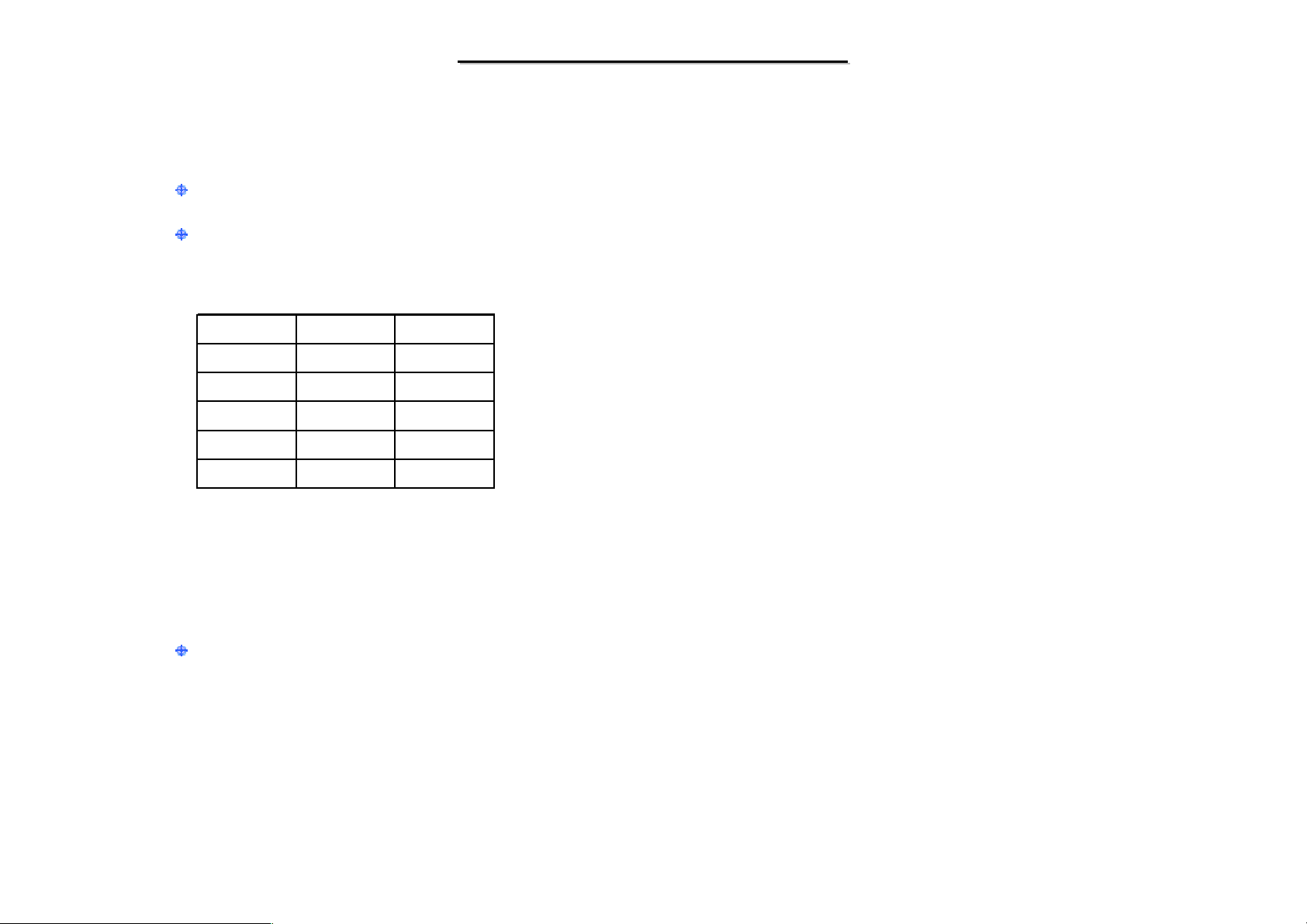
64MB 400/33/266MHz DIMM DDR Memory expandable to 1024 MB (2 DDR slot )
Support 184pin DDR DIMM Memory
Table 2. Memory Expansion Capacity
Slot1 Slot2 Slot3
256MB 0MB 256MB
256MB 256MB 512MB
512MB 0MB 512MB
512MB 256MB 768MB
512MB 512MB 1024MB
8599
8599
N/B Maintenance
N/B Maintenance
1.2.5 I/O Ports
Audio Ports
- Microphone In & Line Out
- Built in 2 high quality internal speaker (2W)
- Built in 1 mono microphone
30
Page 32
8599
8599
N/B Maintenance
N/B Maintenance
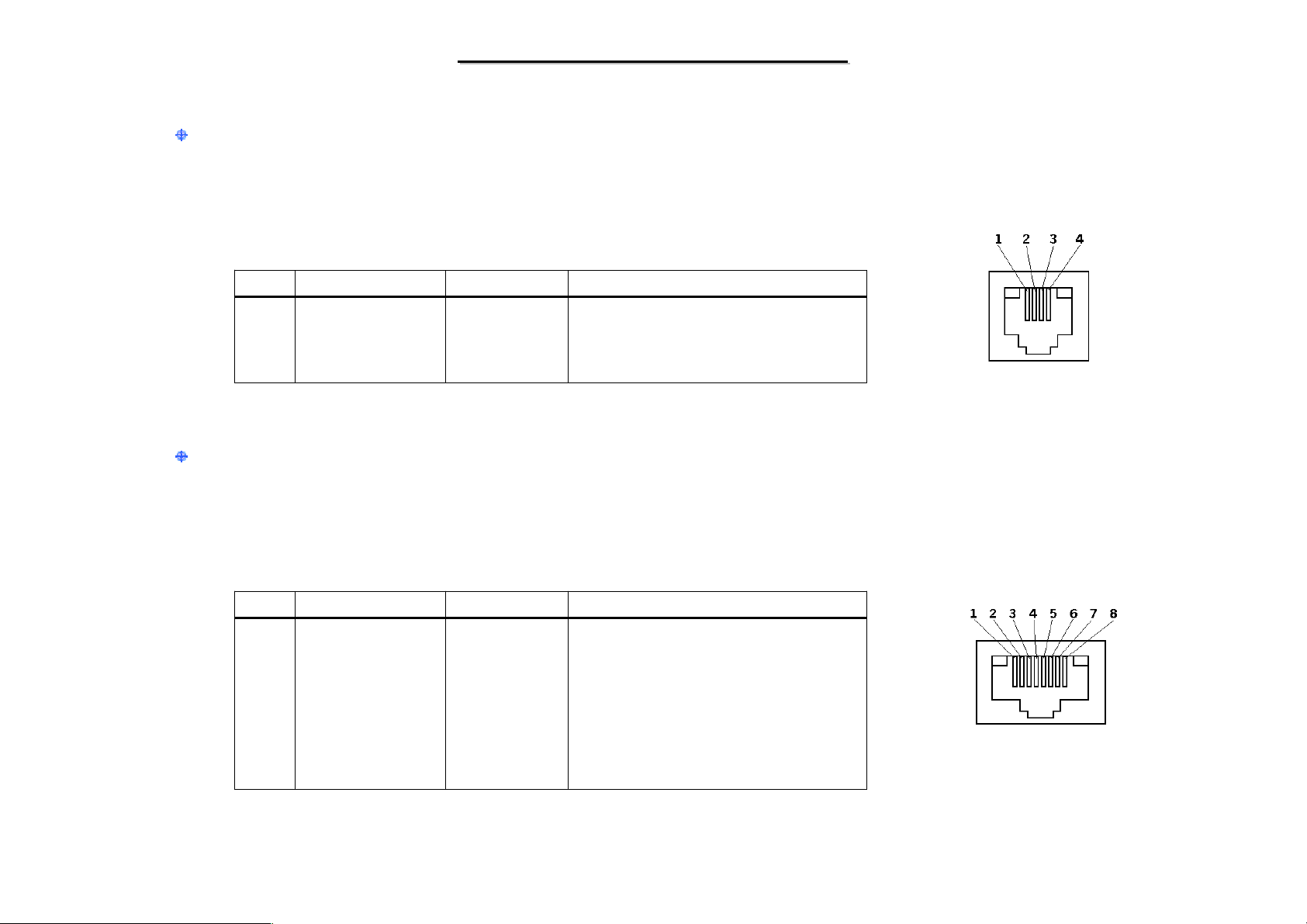
RJ-11
- Connection to Modem Daughter Board Connector
Table 3. Modem Port
Pin Signal Name Direction Description
1 NC - No Connect
2 LINE + I/O Phone Line Positive
3 LINE - I/O Phone Line Negative
4 NC - No Connect
RJ-45
- Connection to On-Board NIC controller
Table 4. LAN Port
Pin Signal Name Direction Description
1 TX+ Out Transmit Data Ring
2 TX- Out Transmit Data Tip
3 RX+ IN Receive Data Ring
4 TERM1 - Internal termination resistor
5 TERM2 - Internal termination resistor
6 RX IN Receive Data Tip
7 TERM3 - Internal termination resistor
8 TERM4 - Internal termination resistor
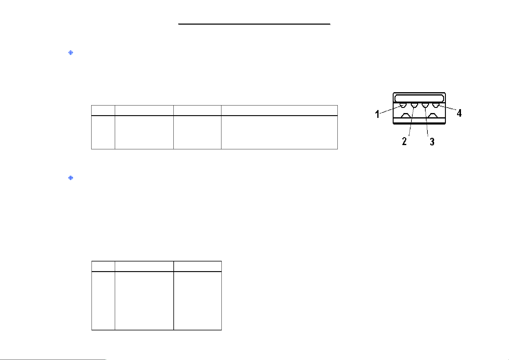
Figure 1 . Modem Connector
Figure 2 . LAN Connector
31
Page 33
8599
8599
USB Ports
- Six industry standard USB 2.0 ports
Table 5. USB Port
Pin Signal Name Direction Description
1 VCC - USB Device Power (+5VDC)
2 DATA- I/O Balanced Data Negative
3 DATA+ I/O Balanced Data Positive
4 GND - Ground
7 Pins S-VIDEO Port for TV-Out
N/B Maintenance
N/B Maintenance
Figure 3 . USB Connector
- Support up 1024*768 resolution
- Support PAL and NTSC system
- Support composite Output by a transfer cable(RCA)
Table 6. S-Video Port
Pin Signal Name Direction
1 GND 2 NC 3 GND 4 LUMA O
5 NC 6 CRMA O
7 COMP O
32
Page 34
8599
8599
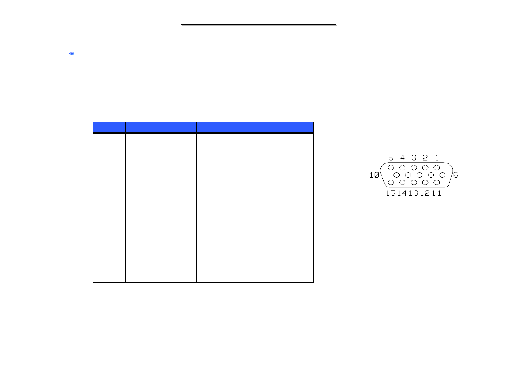
CRT Ports
- Standard VGA compatible port
- DDC1 and DDC2B compliant (RCA)
Table 7. CRT Connector
PIN SIGNAL DESCRIPTION
1 RED Red analog video output
2 GREEN Green analog video output
3 BLUE Blue analog video output
4 Monitor Sense Monitor Sense
5 GND Ground
6 GND Ground
7 GND Ground
8 GND Ground
9 VCC +5VDC
10 GND Ground
11 Monitor Sense Monitor Sense
12 CRT DATA Data from DDC monitor
13 HSYNC Horizontal Sync control
14 VSYNC Vertical Sync control
15 CRT CLK Clock to DDC monitor
N/B Maintenance
N/B Maintenance
Figure 4 . CRT Connector
33
Page 35

8599
8599
1.2.6 PC Card Slot
One Type II/I slot supporting the 1997 PC Card standard,and including full R2 (16-bit) and 32-bit Cardbus data
transfer
TI PCI1410A (PCMCIA Controller) & TI TPS2211A (Power Switch)
1.2.7 Graphical Subsystem
Integrate Real256E GPU +SIS301LV Video Bridge
1.2.8 Display
N/B Maintenance
N/B Maintenance
Internal LCD Display is 15” TFT XGA panel
External Video refresh rate of up to 85Hz supported
- Vertical refresh frequencies to meet VESA requirements
- Simultaneous video in specified video modes – switchable with hot key
1.2.9 LEDs Indiactor
CDROM & HDD & NUM & CAP & SCROLL & WLAN
AC & BAT & CHARGE
34
Page 36

8599
8599
N/B Maintenance
N/B Maintenance
1.2.10 Read Only Memory (BIOS Flash)
Fully compatible with industry standard software including Windows 2000 & Windows XP
Fully supports APM V1.2 and latest ACPI specification
2Mb Flash BIOS
Inside BIOS core
1.2.11 Power Management Features
Local standby mode (Individual devices such as HDD, graphics controller,LCD etc.. )
CPU Idle mode (Including ACPI modes C1 and C2)
Suspend mode (Including S1 and S3 ACPI modes)
Fully APM V1.2 compliant
Fully ACPI V1.1 compliant
Hibernate for Windows XP
Thermal management
Fully US EPA Energy Start compliant
35
Page 37
8599
8599
1.2.12 Keyboard Controller
Winboard W83L950D
1.2.13 Buttons
Power on bin
1.2.14 Modem
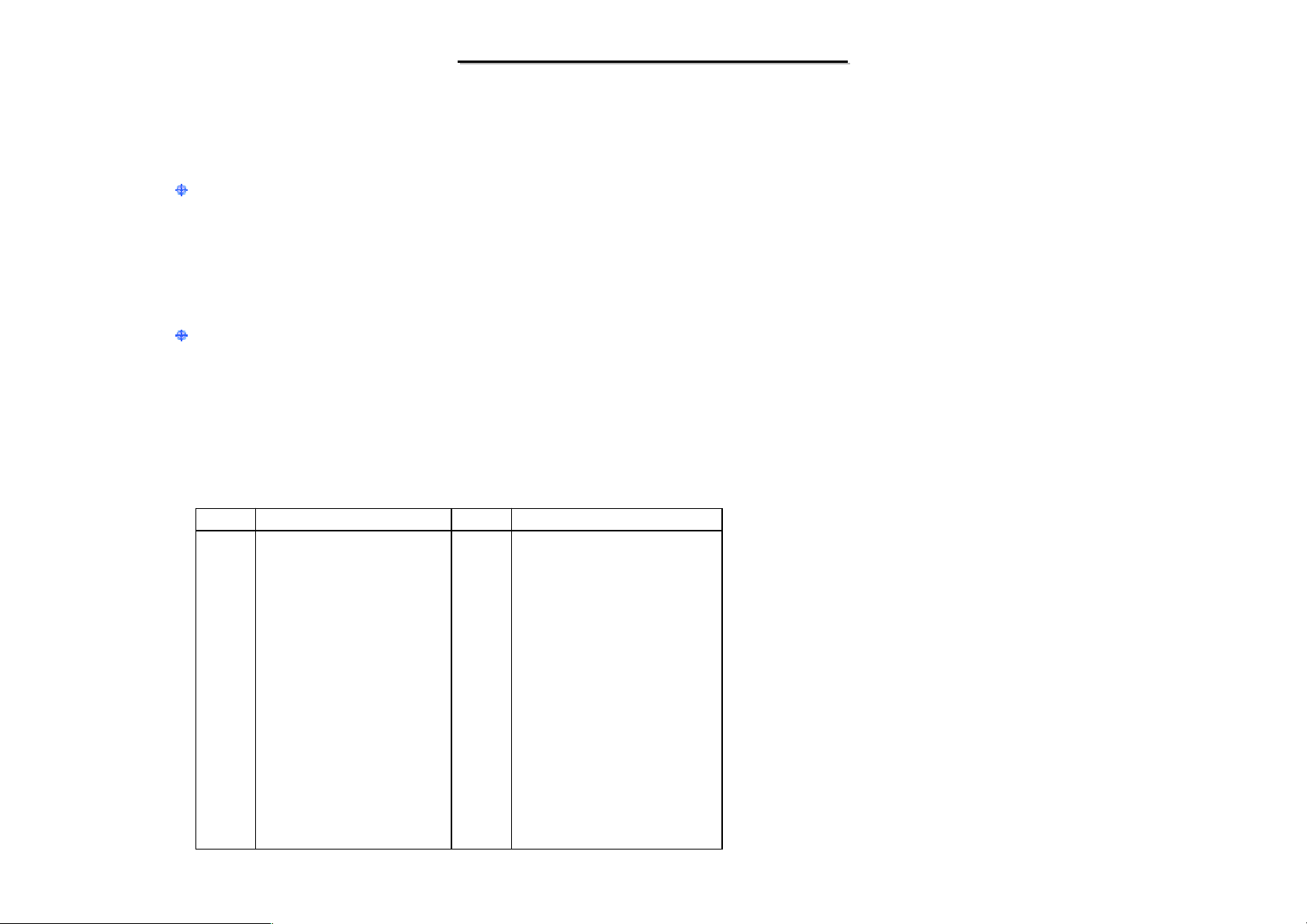
Table 8. Modem Daughter Board Connector
N/B Maintenance
N/B Maintenance
PIN SIGNAL NAME PIN SIGNAL NAME
1 MONO_OUT 2 NC
3 GND 4 MODEM_SPK
5 NC 6 NC
7 NC 8 GND
9 NC 10 +5V
11 NC 12 NC
13 NC 14 NC
15 GND 16 Pull Up to +3V
17 +3V 18 +5V
19 GND 20 GND
21 +3V 22 ACSYNC
23 ACSDOUT 24 MSDIN
25 -ACRST 26 MSDIN
27 GND 28 GND
29 GND 30 ACBITCLK
36
Page 38
8599
8599
1.3 Electrical Characteristic
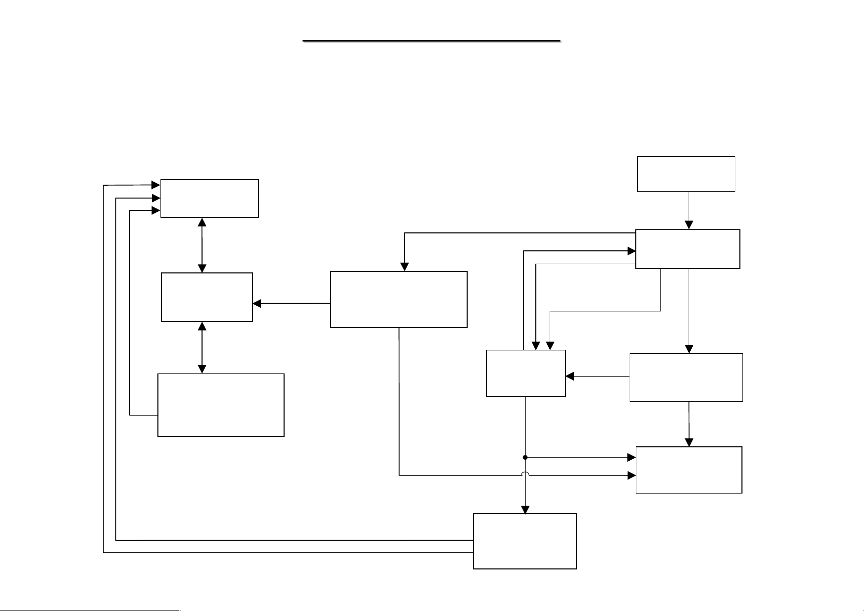
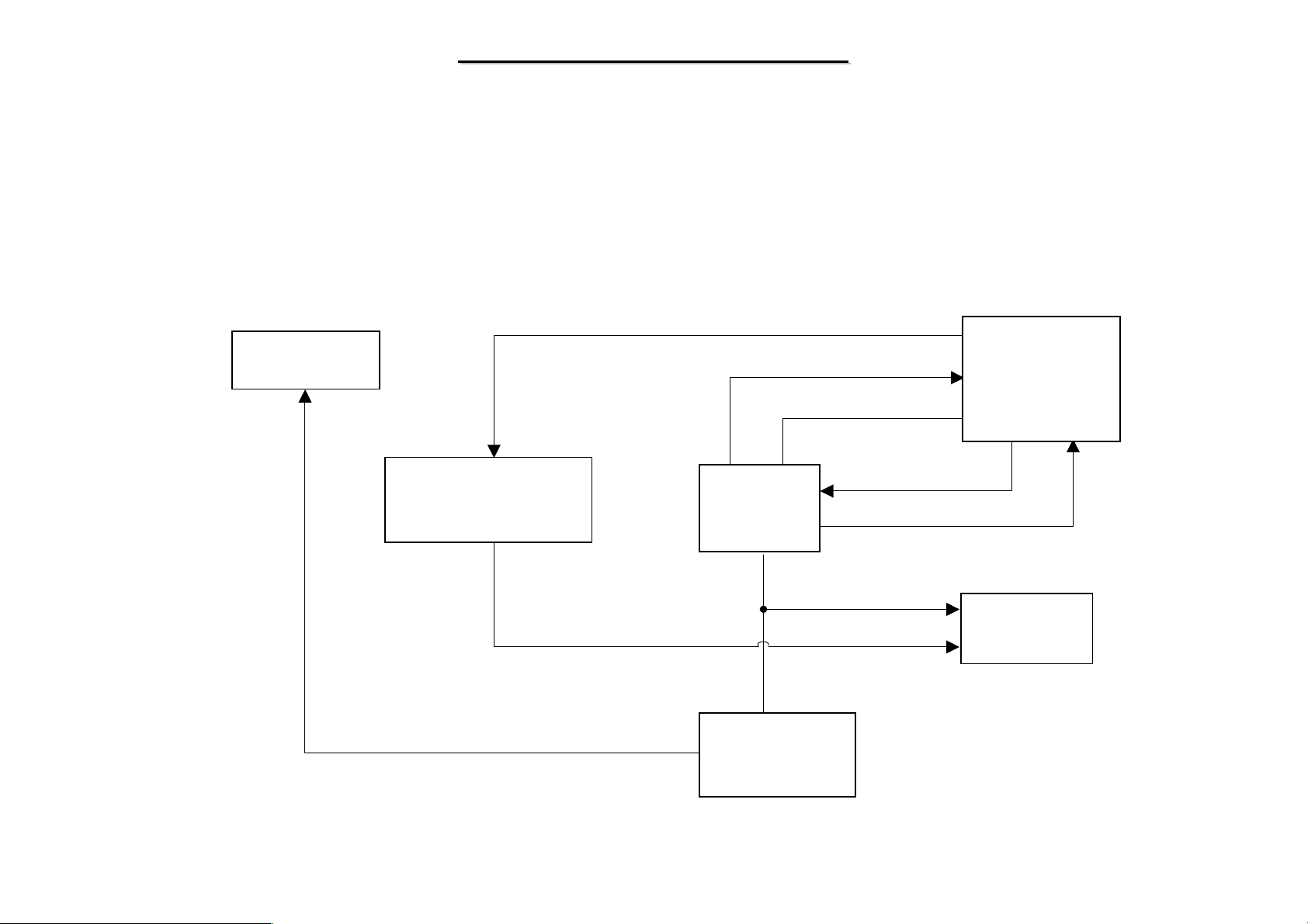
1.3.1 Power On Sequence
N/B Maintenance
N/B Maintenance
CPU
VCCPVID(7)
LDO
CPU_CORE_EN(8)
DC TO DC Converter
+VCC_CORE
+5VS
8599 Power on Sequence Flow Chart
DC TO DC Converter
+12VS/+5VS/+3VS/+1.5VS/
VDD_MEN2.5/+1.8VS/+1.5VS/
+1.25_DDR
South Bridge
SIS963L
Main power(6)
PS ON#(5)
SISPWRBTN#((4)
H8_PWROK(9)
AUXOK(3)
PCIRST#(10)
Press Power Button
Power BTN#(1)
Embeded Controller
W83L950D
PWR_ON(2)
DC to DC Converter
+2.5V_DDR/1.8V/+3V/
+5V/+12V/+1.5V
Standby_Power
CPUPWRGD(11)
CPURST#(12)
MAIN_POWER
System
North Bridge
SiS M661FX
37
Page 39
8599
8599
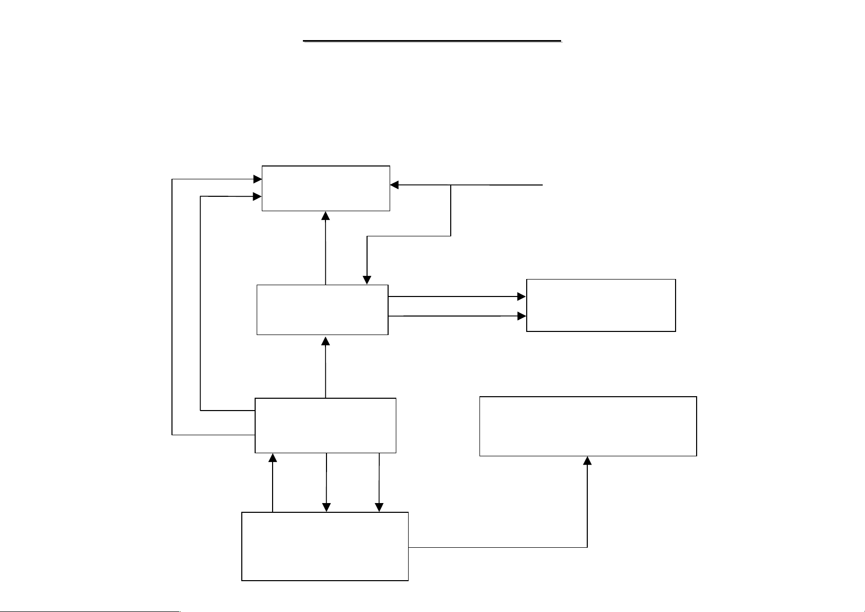
1.3.2 Power Off Sequence
8599 Power off Sequence Flow Chart
N/B Maintenance
N/B Maintenance
MAINPWR(5)
CPU
DC TO DC Converter
+12VS/+5VS/+3VS/+1.5VS/
VDD_MEN2.5/+1.8VS/+1.5VS/
+1.25_DDR
MAIN_POWER
CPURST#(4)
South Bridge
SIS963L
North Bridge
SiS M661FX
PS ON#(1)
SISPWRBTN#(4)
H8_PWROK(2)
S3AUXSW#(6)
PCIRST#(3)
Embeded Controller
W83L950D
System
38
Page 40
8599
8599
N/B Maintenance
N/B Maintenance
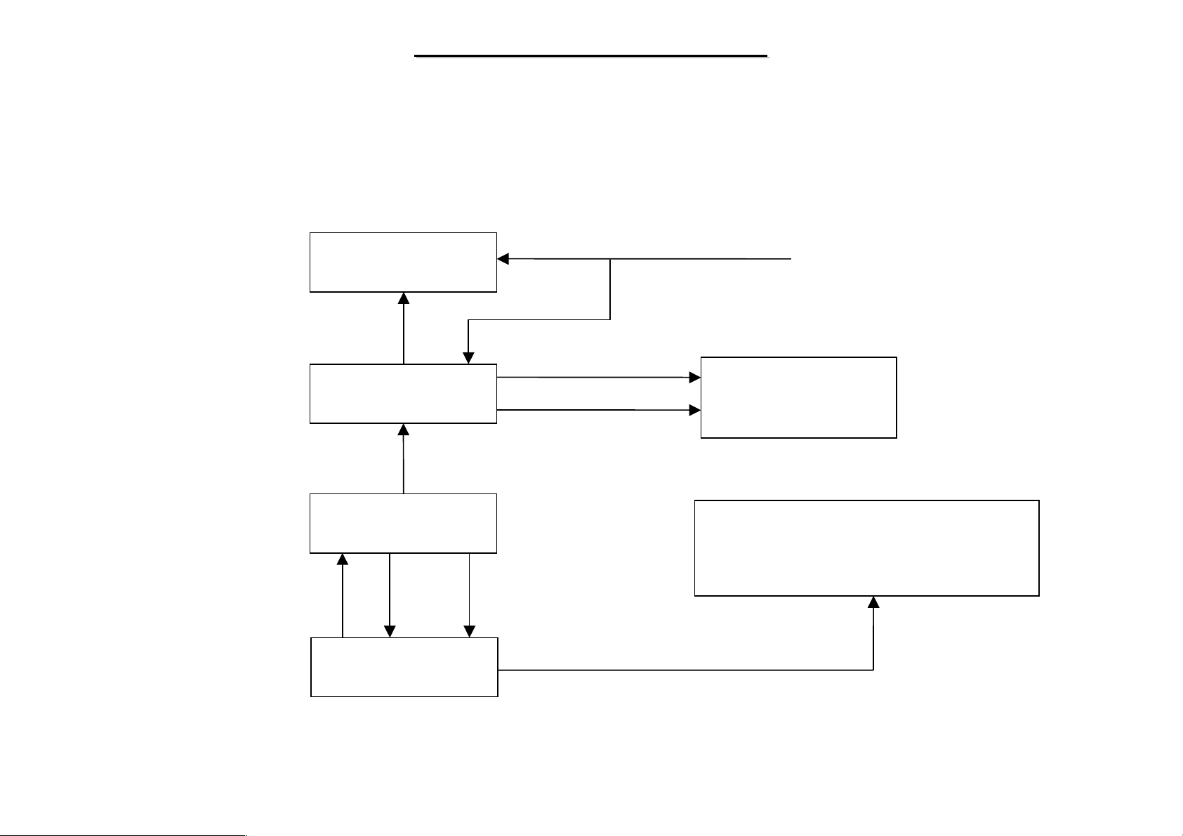
1.3.3 Suspend To RAM Sequence
8599 STR Sequence Flow Chart
SLP#(6)
H_STPCLK#(2)
CPURST# (10)
North Bridge
SiS M661FX
PCIRST# (9)
South Bridge
SiS963L
CPU
Sleep Event (1)
Self-Refresh (3)
CKE[0:5] (4)
DDR SO-DIMM
DC TO DC Coverter
+12VS/+5VS/+3VS/+1.5VS/VDD_MEM2.5/
+1.8VS/+1.25_DDR
H8_
PWROK(8)
Embeded Controller
PS_ON#(7)
W83L950D
S3AUXSW#(5)
MAINPWR(11)
39
Page 41
8599
8599
N/B Maintenance
N/B Maintenance
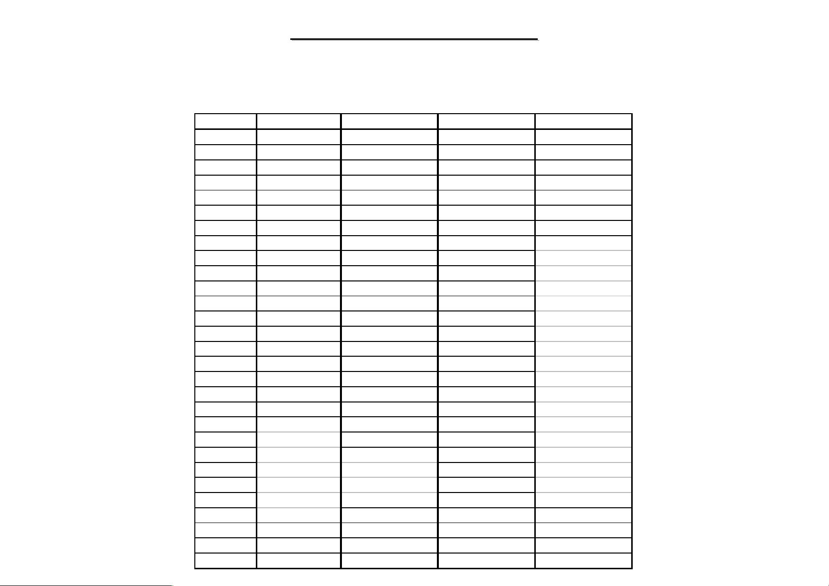
1.3.4 Resume from Suspend To RAM Sequence
8599 Resume From STR Sequence Flow Chart
CPURST# (6)
H8_PWROK (4)
CPU
North Bridge
SIS M661FX
PCIRST# (5)
South Bridge
SIS 963L
PS_ON# (2)
Embeded Controller
W83L950D
Wakeup Event (1)
Self-refresh (3)
CKE#[0:5] (7)
S3AUXSW# (7)
DDR SO-DIMM
DC To DC Converter
+12VS/+5VS/+3VS/+1.5VS/VDD_MEM2.5/
+1.8VS/+1.5VS/+1.25_DDR
MAINPWR (3)
40
Page 42

8599
8599
1.3.5 Power Consumption Of Suspend Mode
Suspend to RAM < 40mA
Suspend to Disk / Soft-Off /Mechanical Off < 1mA
N/B Maintenance
N/B Maintenance
41
Page 43
8599
8599
N/B Maintenance
N/B Maintenance
1.4 Appendix 1: SiS963L GPIO Definitions
Pin Nam e Pin Function Signal Nam e Typ e Define Pow er Plan
GPIO0 GPIO ENBKL_ NA ME O MA IN
GPIO1 GPIO FLASH O MAIN
GPIO2 GPIO SB_THRM # I MA IN
GPIO3 GPIO EXTSMI# I MAIN
GPIO4 GPIO CLKRUN# I/O MA IN
GPIO5 GPIO MPCI_PD# I MAIN
GPIO6 GPIO SPK_OFF# O MAIN
GPIO7 GPIO GPW AK# T/P A UX
GPIO8 GPIO WAKE_UP# I AUX
GP IO 9 GP IO S CI # I A U X
GP IO 10 GP IO CR T_ I N# I A U X
GPIO11 GPIO STP_PCI# O AUX
GP IO 12 GP IO CP U_ S TP # O A U X
GP IO 13 GP IO DP RS LPVR O A U X
GPIO14 GPIO LCD_ID0 I AUX
GP IO 15 GP IO GM UXS EL T / P A U X
GP IO 16 GP O CPU PER F# O A U X
GP IO 17 GP O N/ A T / P A U X
GP IO 18 GP O N/ A T / P A U X
GP IO 19 GP IO S M BCLK I / O A U X
GP IO 20 GP IO S M BDA T A I/ O A U X
GP IO 21 GP I GP IO 21 _ EES K A U X
GP IO 22 GP I GP IO 22 _ EED I A U X
GP IO 23 GP I GP IO 23 _ EED O A U X
GP IO 24 GP I GP IO 24 _ EECS A U X
APICD0 NC MAIN(GTL LEVEL
APICD1 NC MAIN(GTL LEVEL
APICCLK NC MA IN
OC5 GPI AUX
42
Page 44
8599
8599
N/B Maintenance
N/B Maintenance
1.5 Appendix 2: Keyboard Controller Pin Definitions (1)
Pin Port Signal Name Type Descriptio n
39~54 GP17~GP0 KO[0..15] O Keyboard M a t rix
55~62 GP37~GP30 KI[7..0] O Keyboard Matrix
65~68 GP85~GP82 LAD[0..3] I/O LPC BUS
70
69
64
63
17
15
14
23
22
19
3
2
27
26
13
12
16
18
21
20
9
8
7
6
GP80 PCI_KBCLK I LPC CLK
GP81 SERIRQ O Serial IRQ
GP86 KBCLRST# I LPC Res et
GP87 LFRAME# I/O LPC FRAM E
GP50 MAINPWR O We use this signal to control "VS" power on/off. HI:ON,LOW:OFF
GP52 SUSB# I STR Indicator signal
GP53 ADEN# I ADAPTOR IN
GP42 SW _+5VA O Switch +5VA
GP43 COVER_SW # I LCD Co v er s witch
GP46 SCI O Connect to South Bridge (SiS963L) to system configuration interrupt (ACPI mode)
GP76 BAT_DATA I/O SMBUS DATA for LM86 themal s ensor & BATT THERMAL
GP77 BA T_ CLK I/O SMBUS CLK for LM87 themal s e n s or & BA TT THERMA L
GP40 FAN0 O Control CPU FA N ON & Tum ON/OFF Du ty
GP41 FAN1 O Control Sys tem D/D FAN (Second FAN) ON & Tum ON/OFF Duty
GP54 FAN0_SPD0 I Return FA N0 (CPU FAN) Speed
GP55 FAN0_SPD1 I Return FA N0 (Second FA N) Speed
GP51 BATT_DEAD# I Indicated the battery capacity is not enough to power on system
GP47 PWRON O Con trol Sys tem Power ON/OFF
GP44 NUM# O Keyboard Number Lock indicator
GP45 CAP# O Keyboard CAPs Lock indicator
GP70 T_DATA I/O Conneter to touch Pad DATA
GP71 LEARNING# I Battery dis charg e con trol
GP72 SIS_PWRBTN# O Power Button Signal to SiS963L
GP73 T_CLK I/O Connect to Touch Pad clock
43
Page 45
8599
8599
N/B Maintenance
N/B Maintenance
1.5 Appendix 2: Keyboard Controller Pin Definitions (2)
Continue to the previous page
Pin Port Signal Name Type De scription
5
4
38
37
36
35
34
33
32
31
11
10
1
80
79
78
77
76
75
74
25
28
29
72
71
GP74 PWROK O System Power Good
GP75 PSON#_SB I System inter S4~S5,Positive Logic
GP20 SB_THRM# O TO SiS963L,Regustang the sysytem toenter power mangmentmode,Clock Throtting
GP21 WAKE_UP# O Connect to South Bridge (SiS963L) to wake up system
GP22 BATT_G# O The indicator when battery in charging
GP23 BATT_R# O The indicator when battery in charging
GP24 EXTSM# O Connect to South Bridge (SiS963L) to system management interrupt (Non-ACPI mode)
GP25 BATT_POWER# O The indicater when power supply from Battery
GP26 SCROLL# O Keyboard scroll lock indicator
GP27 AC_POWER# O The indicator when power supply from AC-Adapter
GP56 BLA DJ O Ba ck/ Ligh t Ad iju st Co n tro l
GP57 CHG_I O Supply current to Battery
GP60 PWRBTN# I Po wer Switch Signal to KBC
GP61 VRM PW RGD I CP U Po we r Go o d
GP62 + 3 V I
GP63 BAT_TEMP I Report Battery Thermal
GP64 BA T_ VOLT I Re p o rt Ba tt e r y Volt ag e
GP65 I_LIMIT I FOR BATTERY CHA RGE I limit
GP66 I_CHG I Battery charge current
GP67 I_DISCHG I Battery disch arge current
RESET# RESET# I KBC Re s et
XIN XIN
XOUT XOUT
VREF +3VA
VCC + K B C_ VDDA
44
Page 46
8599
8599
N/B Maintenance
N/B Maintenance
1.6 Appendix 3: Audio Performance
8599 meet all the following items
Table 9. Digital Playback (PC-D-A) for Line Output
Test Items Mobile System
Full Scale Output Voltage
Sample Frequency Accuracy
Frequency Response (44.1ks/sec)
Frequency Response (48ks/sec)
Dynamic Range (SNR)
THD+N
Cross-talk
≧0.7Vrms (3.3V audio)
0.1%
≦
20Hz~15kHz
20Hz~15kHz
≧70dBFSA
-55dBFS
≦
≧50dB
Table 10. Analog Pass-through(A-A) for Microphone Input to Line Output
Tes t Items Mobile Syste m
Frequency Response
Dynamic Range (SNR)
THD+N
Table 11. Digital Recording(A-D-PC) for Microphone Input
Te st Items Mobile System
Full Scale Input Voltage
Sample Frequency Accuracy
Frequency Response(22.05ks/sec)
Dynamic Range (SNR)
THD+N
100Hz~12kHz
60dBFSA
≧
≦-50dBFS
≧100mVrms
≦0.1%
100Hz~8.8kHz
≧60dBFSA
≦-50dBFS
45
Page 47
8599
8599
N/B Maintenance
N/B Maintenance
2. System View and Disassembly
2.1 System View
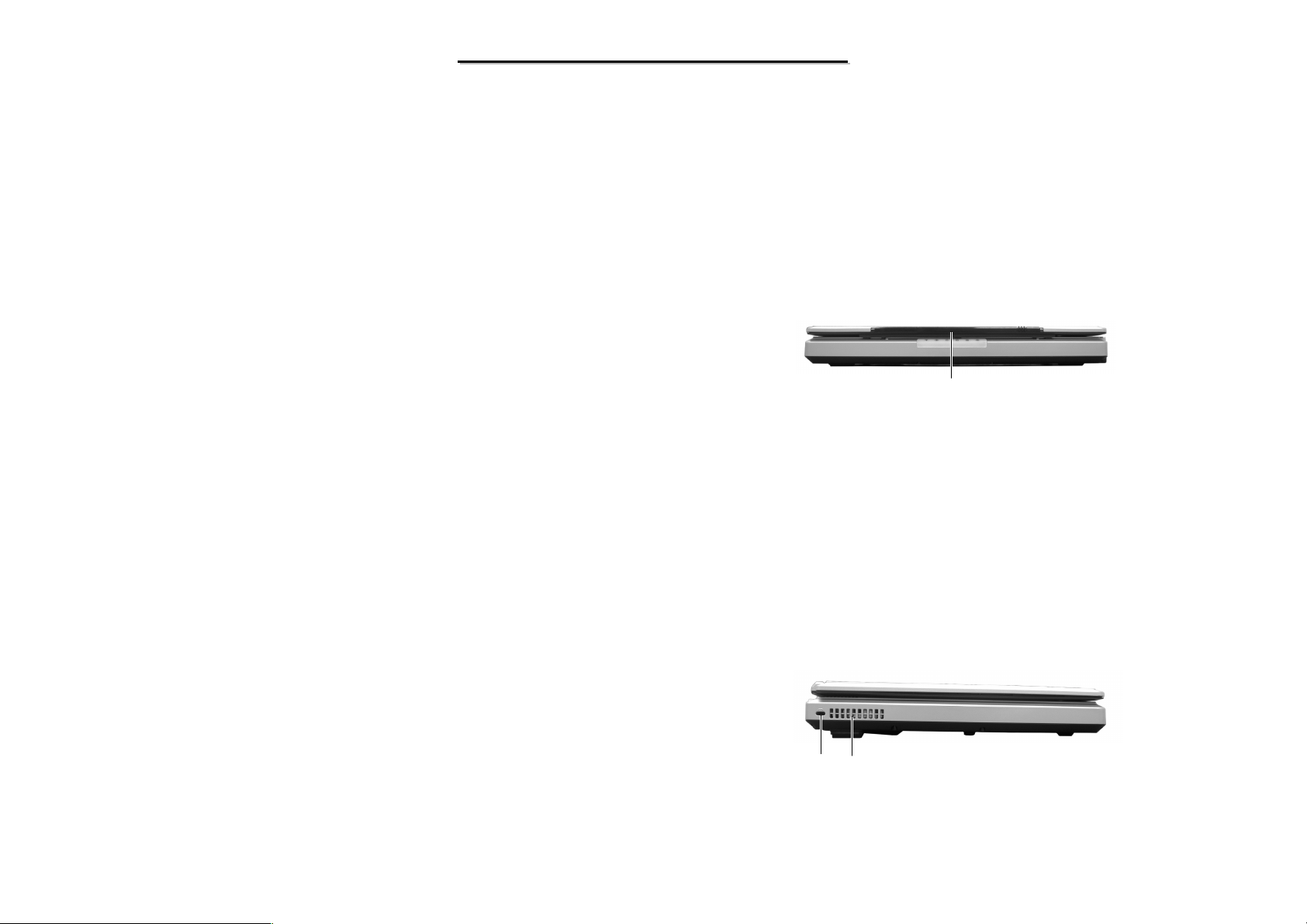
2.1.1 Front View
1
Top Cover Latch
1
2.1.2 Left-side View
1
Lock
2
Ventilation Openings
1
2
46
Page 48
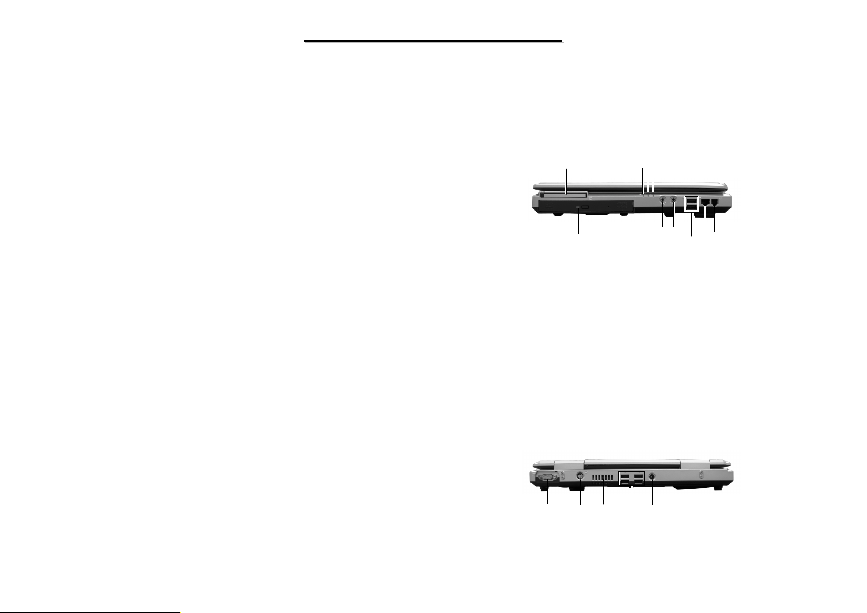
2.1.3 Right-side View
1
CD/DVD driver
2
Line out jack
3
MIC in jack
4
USB port *2
5
RJ-45 connector
6
RJ-11 connector
7
AC Power Indicator
8
Battery Power Indicator
9
Battery Charge Indicator
10
PC Card slot
8599
8599
N/B Maintenance
N/B Maintenance
10
1
9
8
7
2
3
4
5
6
2.1.4 Rear View
1
VGA port
2
S-Video output connector
3
Ventilation Openings
4
USB port *4
5
Power connector
1
23
4
5
47
Page 49
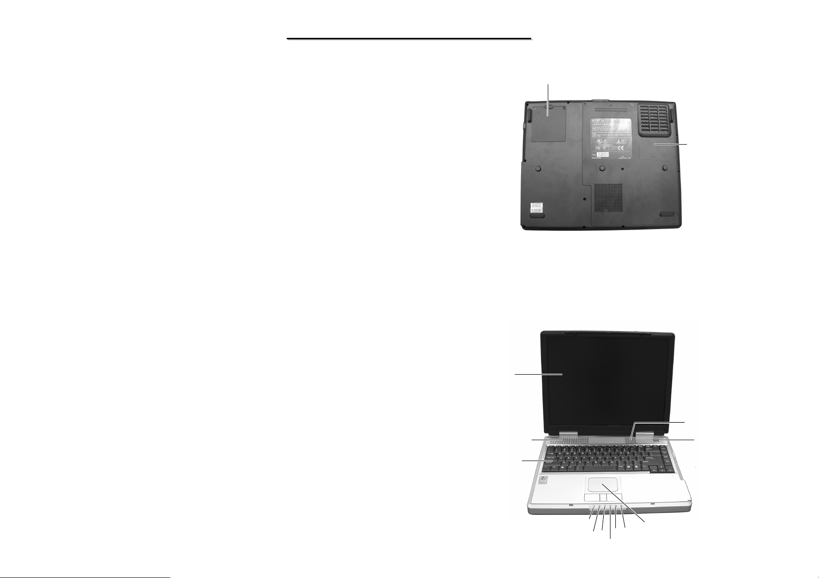
2.1.5 Bottom View
1
Wireless Card cover
8599
8599
N/B Maintenance
N/B Maintenance
1
2
CPU
2.1.6 Top-open View
1
LCD Screen
2
Stereo set
3
Keyboard
4
Caps Lock
5
Wireless Card Indicator
6
CD/DVD-Rom Indicator
7
HDD Indicator
1
3
2
2
2
11
8
Num Lock
9
Caps Lock
10
Scroll Lock
11
Power Button
4
10
9
8
6
5
7
48
Page 50
8599
8599
N/B Maintenance
N/B Maintenance
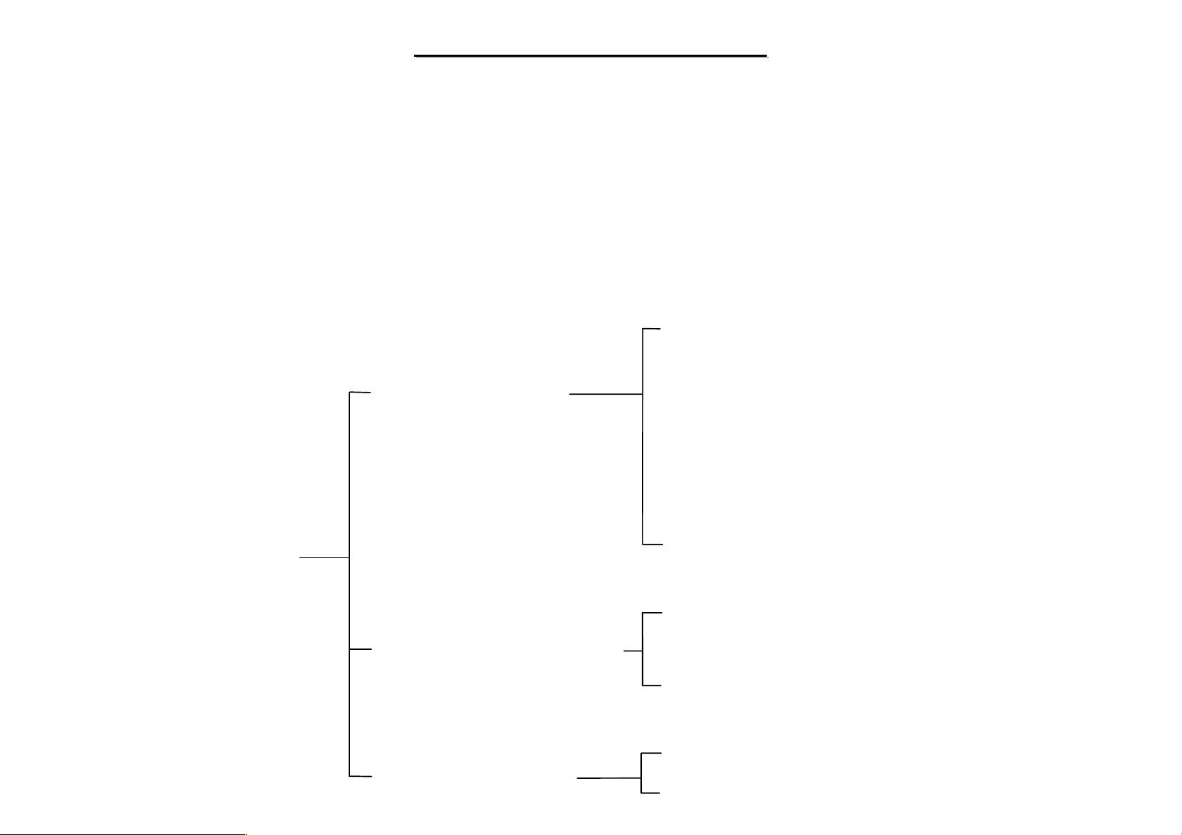
2.2 System Disassembly
The section discusses at length each major component for disassembly/reassembly and show corresponding
illustrations. Use the chart below to determine the disassembly sequence for removing components from the
notebook.
NOTE: Before you start to install/replace these modules, disconnect all peripheral devices and make sure the
notebook is not turned on or connected to AC power.
2.2.1 Battery Pack
2.2.2 Keyboard
NOTEBOOK
Modular Components
LCD Assembly Components
Base Unit Components
2.2.3 CPU
2.2.4 HDD Module
2.2.5 DVD-ROM Drive
2.2.6 DIMM module
2.2.7 Modem Card
2.2.7 LCD Assem bly
2.2.8 Inverter Board
2.2.9 LCD Panel
2.2.10 System Board
2.2.11 Touch Pad
49
Page 51
8599
8599
N/B Maintenance
N/B Maintenance
2.2.1 Battery Pack
Disassembly
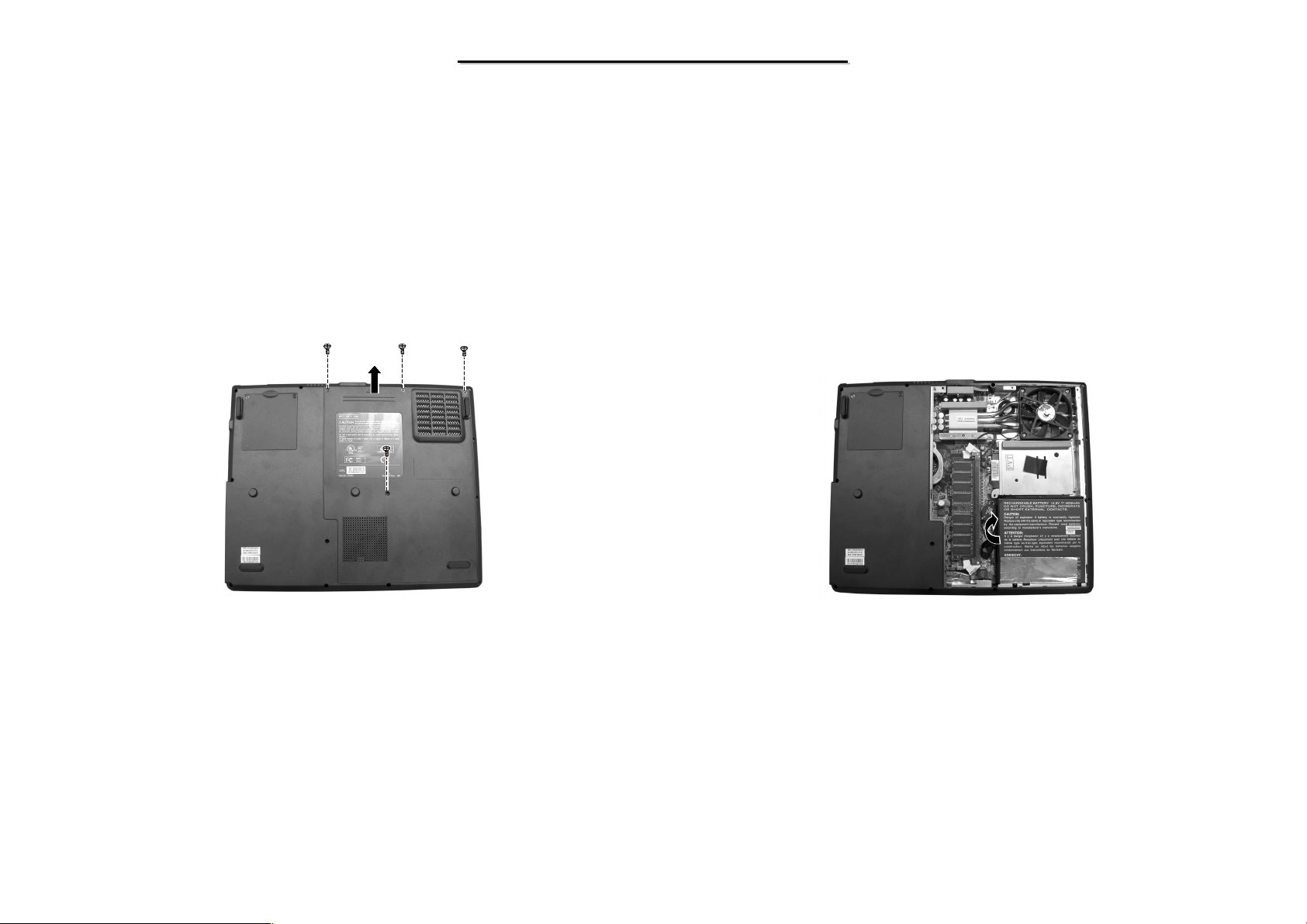
1. Carefully put the notebook upside down.
2. Remove the four screws, then remove the CPU cover. (Figure 2-1)
3. Put up the battery pack, then free the battery pack. (Figure 2-2)
Figure 2-1 Remove the four screws
Reassembly
1. Replace the battery pack into the compartment. The battery pack should be correctly connected when you hear a
clicking sound.
2. Replace the CPU cover and secure the four screws.
Figure 2-2 Remove the battery pack
50
Page 52
8599
8599
N/B Maintenance
N/B Maintenance
2.2.2 Keyboard
Disassembly
1. Remove the battery pack. (Refer to section 2.2.1 Disassembly)
2. Open the top cover.
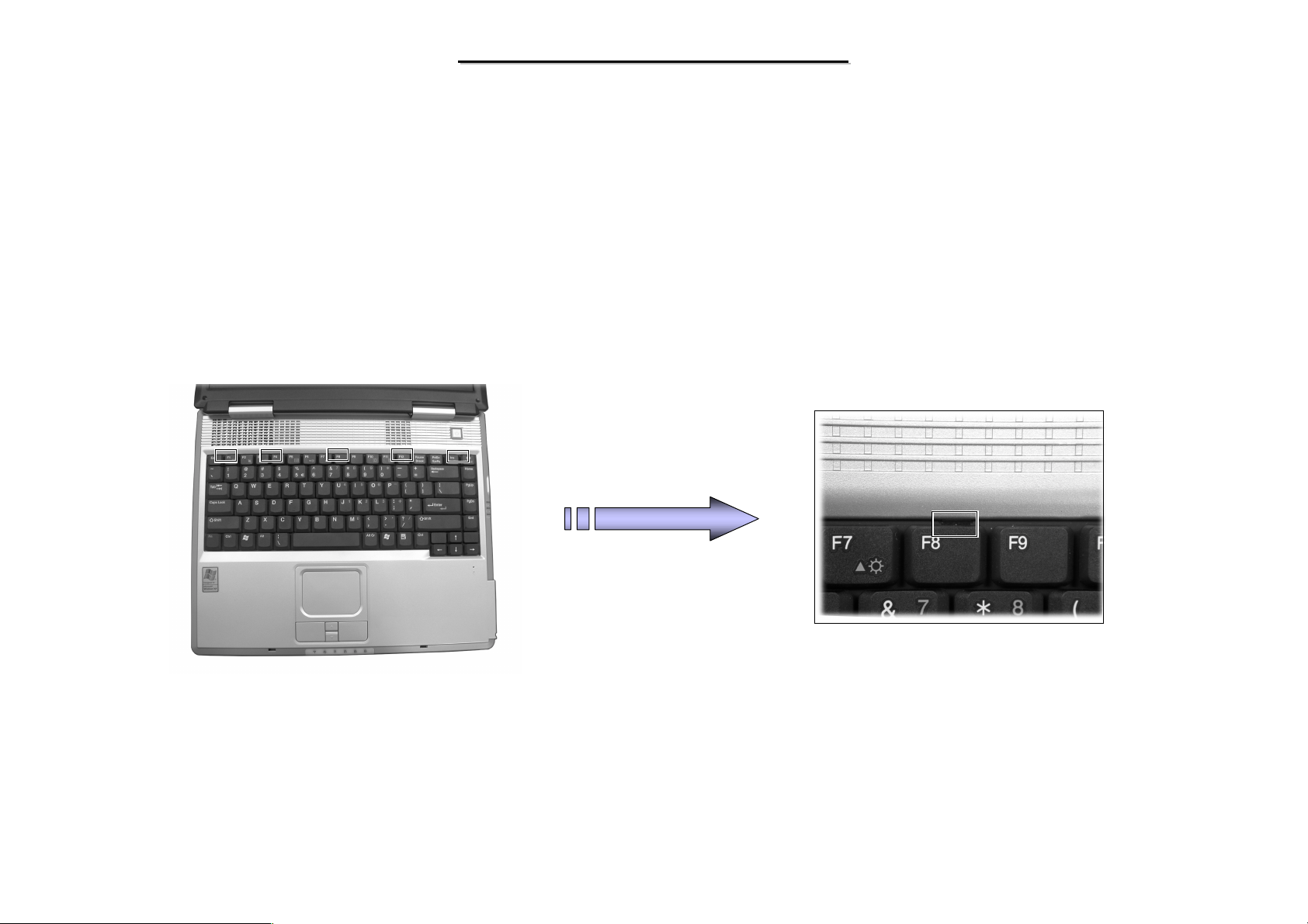
3. Loosen the five latches locking the keyboard. (Figure 2-3)
Figure 2-3 Loosen the five latches
51
Page 53
8599
8599
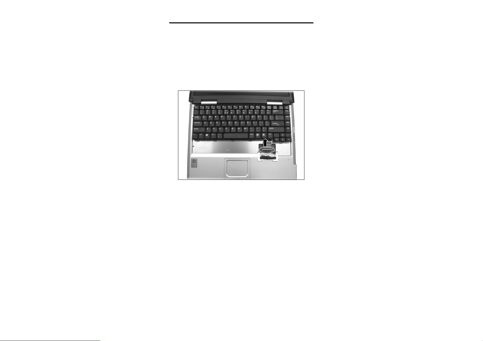
4. Slightly lift up the keyboard and disconnect the cable from the mother board, then separate the keyboard.
(Figure 2-4)
N/B Maintenance
N/B Maintenance
Figure 2-4 Lift up the keyboard and disconnect the cable
Reassembly
1. Reconnect the keyboard cable and fit the keyboard back.
2. Replace the keyboard into place and fasten the five latches.
3. Replace the battery pack. (Refer to section 2.2.1 reassembly)
52
Page 54
8599
8599
N/B Maintenance
N/B Maintenance
2.2.3 CPU
Disassembly
1. Remove the battery pack. (Refer to section 2.2.1 Disassembly)
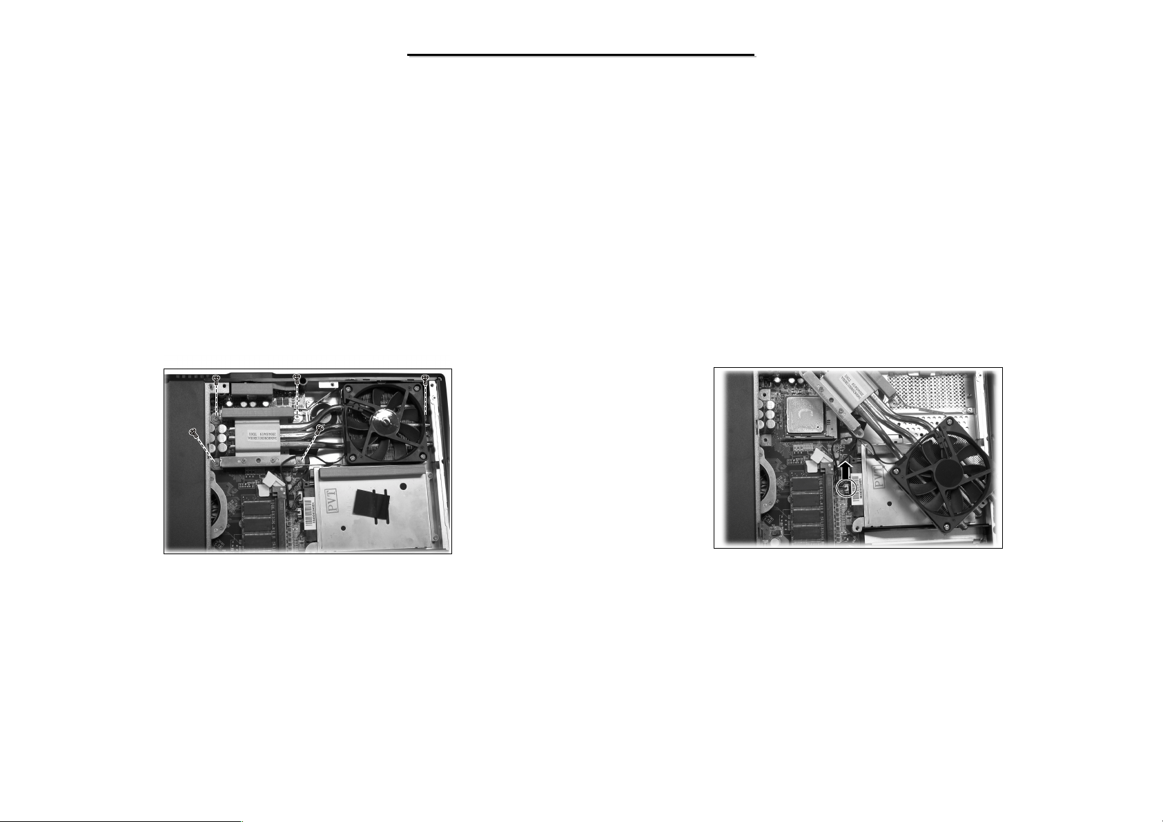
2. Remove five screws that secure the heatsink upon the CPU. (Figure 2-5)
3. Disconnect the fan’s power cord from system board. (Figure 2-6)
Figure 2-5 Remove five screws Figure 2-6 Disconnect the cable
53
Page 55
8599
8599
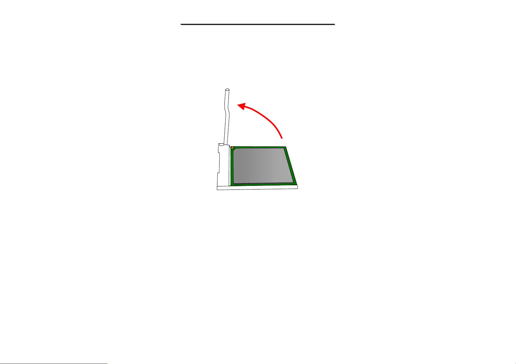
4. To remove the existing CPU, lift the socket arm up to the vertical position. (Figure 2-7)
N/B Maintenance
N/B Maintenance
CPU socket stopper
Figure 2-7 Free the CPU
Reassembly
1. Carefully, align the arrowhead corner of the CPU with the beveled corner of the socket, then insert CPU pins into
the holes. Place the lever back to the horizontal position and push the lever to the left.
2. Reconnect the fan’s power cord to the system board, fit the heatsink onto the top of the CPU and secure with five
screws.
3. Replace the battery pack. (See section 2.2.1 reassembly)
54
Page 56
8599
8599
N/B Maintenance
N/B Maintenance
2.2.4 HDD Module
Disassembly
1. Carefully put the notebook upside down. Remove the battery pack. (Refer to section 2.2.1 Disassembly)
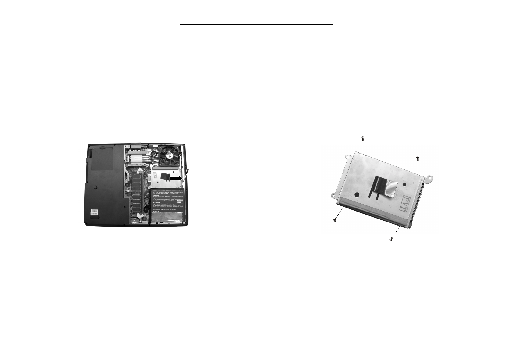
2. Remove two screws fastening the HDD module and slightly lift up HDD module. (Figure 2-8)
3. Remove four screws to separate the hard disk drive from the bracket, free the hard disk driver. (Figure 2-9)
Reassembly
1. Attach the bracket to hard disk drive and secure with four screws.
2. Slide the HDD module into the compartment and secure with two screws.
3. Replace the battery pack. (Refer to section 2.2.1 reassembly)
Figure 2-9 Free the HDD driverFigure 2-8 Remove HDD module
55
Page 57
8599
8599
N/B Maintenance
N/B Maintenance
2.2.5 CD/DVD-ROM Drive
DisassemblyDisassembly
1. Carefully put the notebook upside down. Remove the battery pack. (Refer to section 2.2.1 Disassembly)
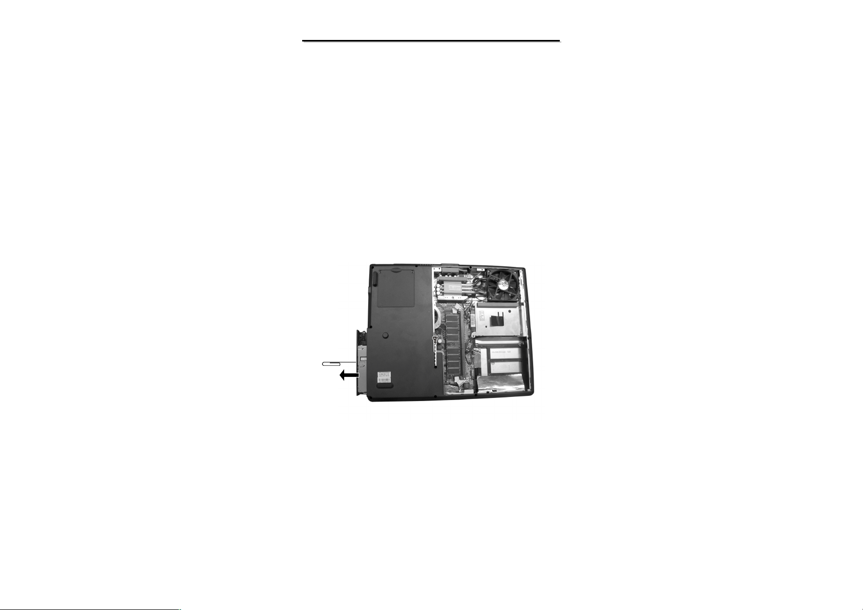
2. Remove two screws fastening the CD/DVD-ROM drive. (Figure 2-10)
3. Insert a small rod, such as a straightened paper clip, into CD/DVD-ROM drive’s manual eject hole () and push
firmly to release the tray. Then gently pull out the CD/DVD-ROM drive by holding the tray that pops out().
(Figure 2-10)
Figure 2-10 Remove the CD/DVD-
ROM drive
Reassembly
1. Push the CD/DVD-ROM drive into the compartment and secure with one screw.
2. Replace the battery pack. (Refer to section 2.2.1 reassembly)
56
Page 58
8599
8599
N/B Maintenance
N/B Maintenance
2.2.6 DIMM Module
DisassemblyDisassembly
1. Carefully put the notebook upside down. Remove the battery pack. (Refer to section 2.2.1 Disassembly)
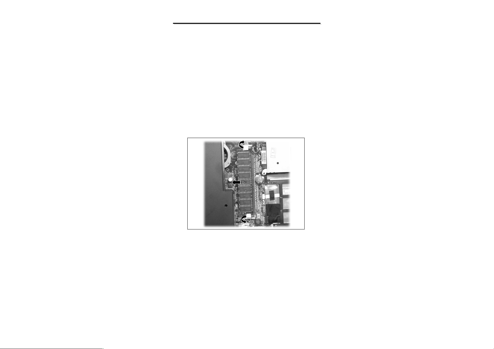
2. To remove the memory module, pull the retaining clips outwards to the unlocked and lift the DIMM module up.
(Figure 2-11)
Figure 2-11 Remove the DIMM module
Reassembly
1. Replace DIMM module and lock it retaining clips.
2. Replace the battery pack. (Refer to section 2.2.1 reassembly)
57
Page 59
8599
8599
N/B Maintenance
N/B Maintenance
2.2.7 Modem Card
Disassembly
1. Remove the battery, keyboard, CPU, hard disk driver, CD/DVD-ROM driver. (Refer to sections 2.2.1, 2.2.2,
2.2.3, 2.2.4, 2.2.5 Disassembly)
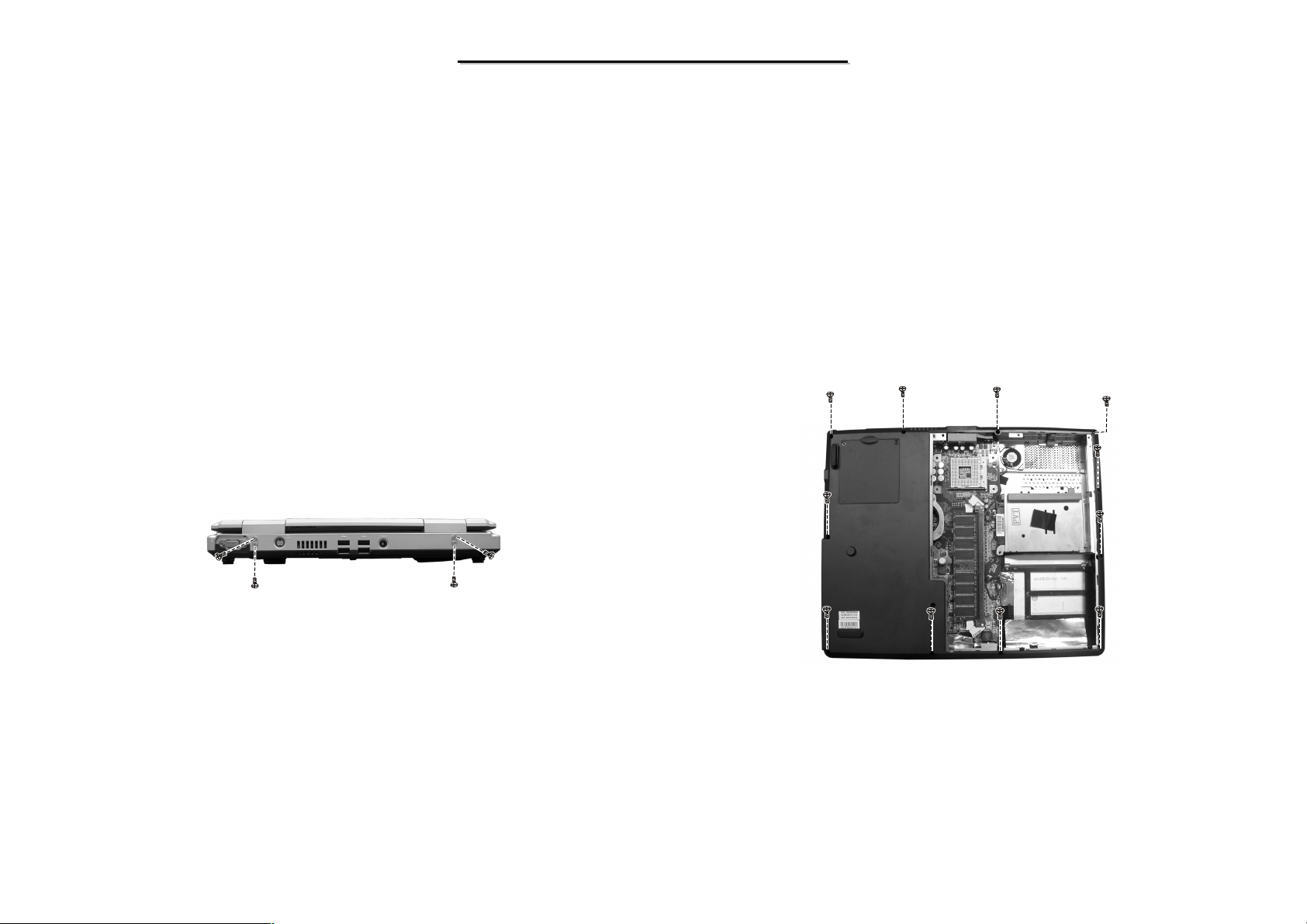
2. Remove the four screws. (Figure 2-12)
3. Remove the eleven screws and put up the housing. (Figure 2-13)
Figure 2-12 Remove eleven screws
Figure 2-13 Free the housing
58
Page 60
8599
8599
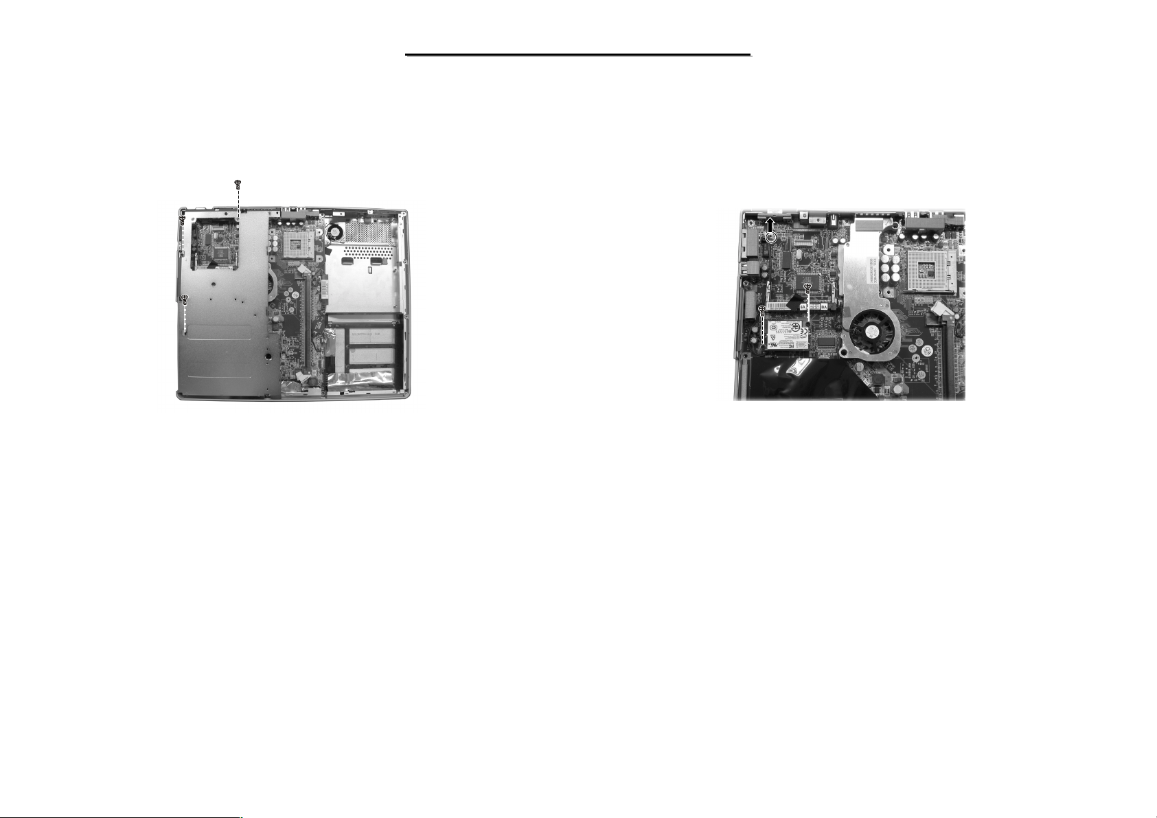
4. Remove three screws and free the bottom shielding. (Figure 2-14)
5. Disconnect the cable and remove the two screws. (Figure 2-15)
N/B Maintenance
N/B Maintenance
Figure 2-14 Free the bottom shielding
Reassembly
1. Replace the modem card and secure two screws.
2. Reconnect the cable to the system board.
3. Replace the bottom shielding and secure the three screws.
4. Fit the top cover and the housing, then secure the fifteen screws.
5. Replace CD/DVD-ROM, HDD, CPU, keyboard and battery pack. (See sections 2.2.5, 2.2.4, 2.2.3, 2.2.2 and 2.2.1
Reassembly)
Figure 2-15 Free the Modem Card
59
Page 61
8599
8599
N/B Maintenance
N/B Maintenance
2.2.8 LCD ASSY
Disassembly
1. Remove the battery pack and keyboard. (See sections 2.2.1 and 2.2.2 Disassembly)
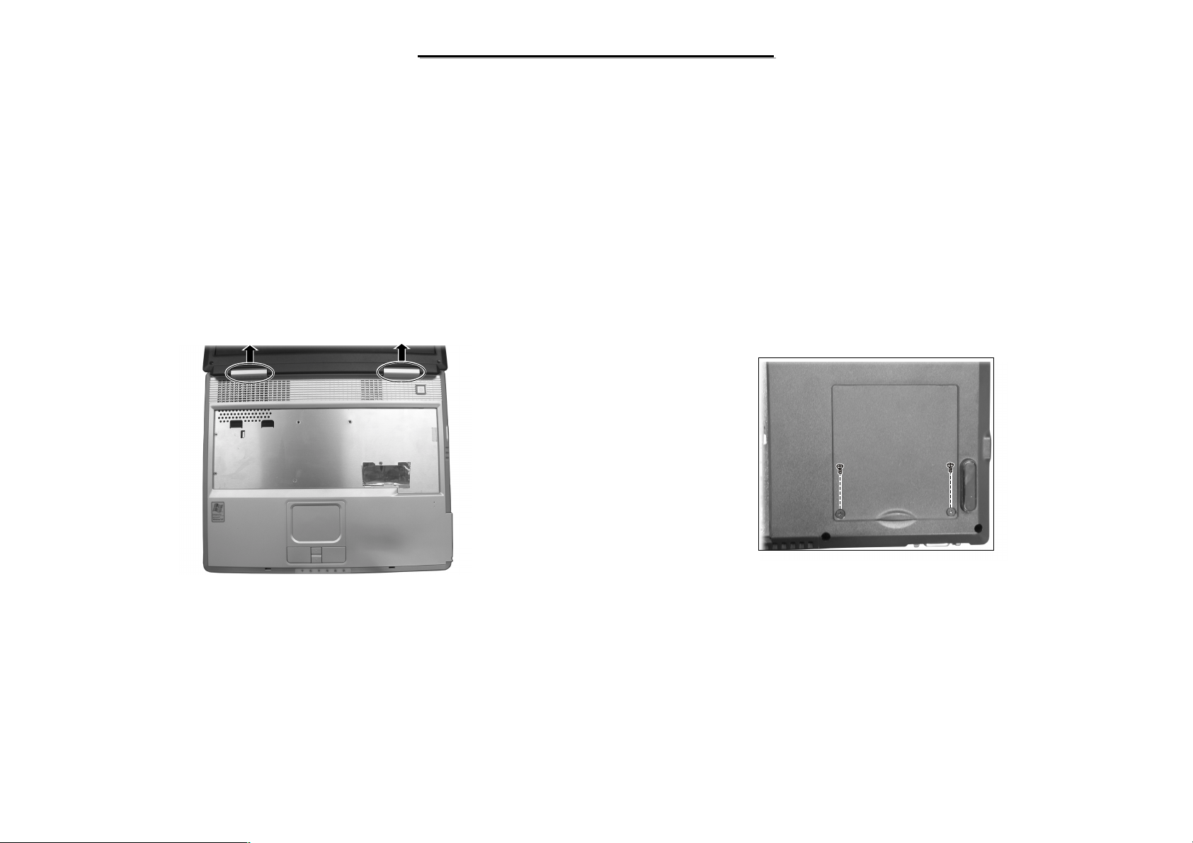
2. Remove two hinge covers. (Figure 2-16)
3. Carefully put the notebook upside down. Remove the two screws fastening the wireless cover. (Figure 2-17)
Figure 2-16 Remove two hinge covers
Figure 2-17 Remove the two screws
60
Page 62
8599
8599
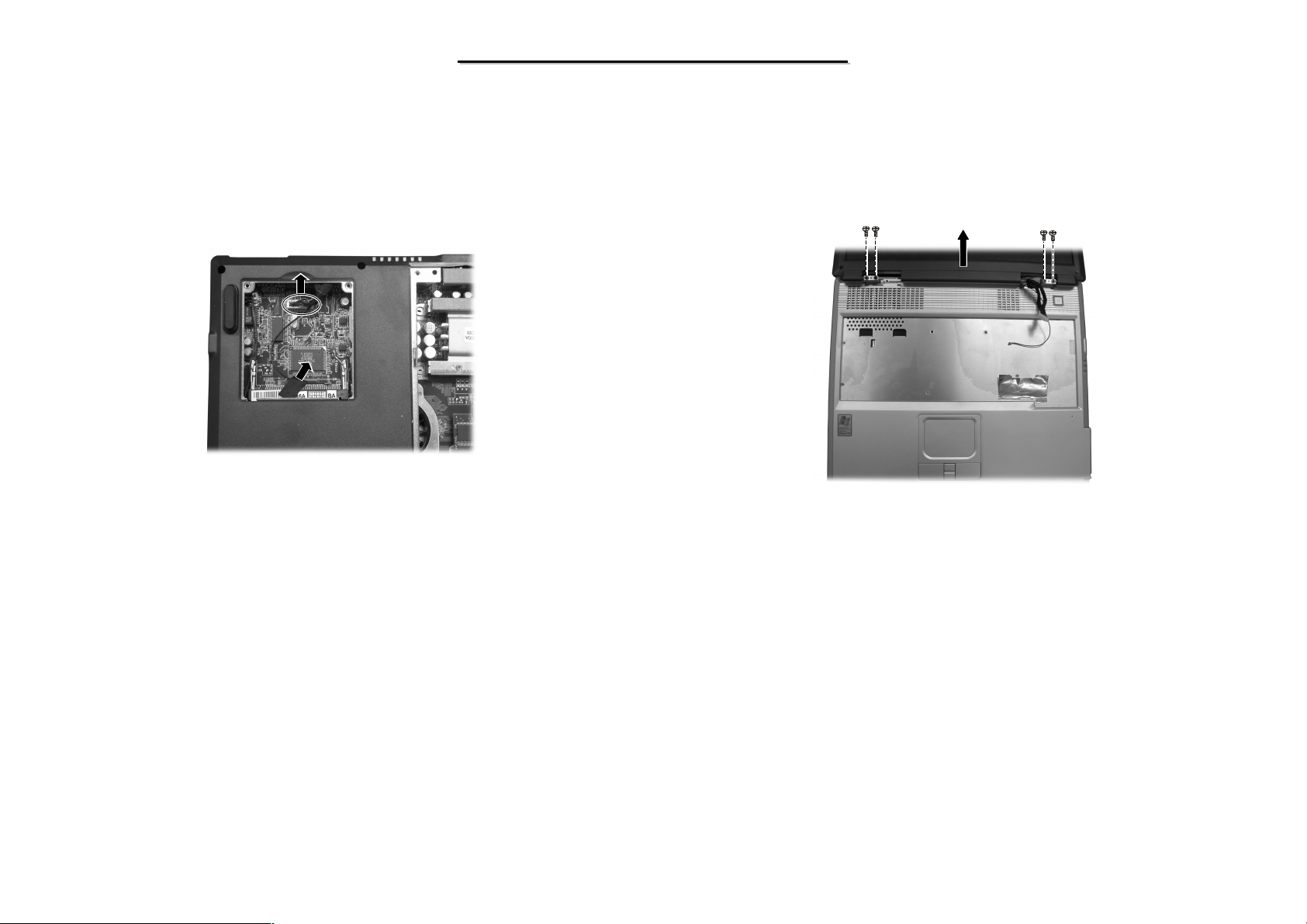
4. Disconnect the LCD cable from the system board and detach the antenna. (Figure 2-18)
5. Remove the four screws and put up the LCD assembly, then free the LCD assembly. (Figure 2-19)
N/B Maintenance
N/B Maintenance
Figure 2-18 Disconnect the LCD cable
Reassembly
1. Attach the LCD assembly to the base unit and secure with four screws, then fit the antenna.
2. Reconnect the one cable to the system board, Then replace the wireless cover and secure two screws.
3. Replace the two hinge covers.
4. Replace the keyboard and battery pack. (Refer to sections 2.2.2 and 2.2.1 Reassembly)
Figure 2-19 Free the LCD assembly
61
Page 63
8599
8599
N/B Maintenance
N/B Maintenance
2.2.9 Inverter Board
Disassembly
1. Remove the battery, keyboard and LCD assembly. (Refer to section 2.2.1, 2.2.2 and 2.2.8 Disassembly)
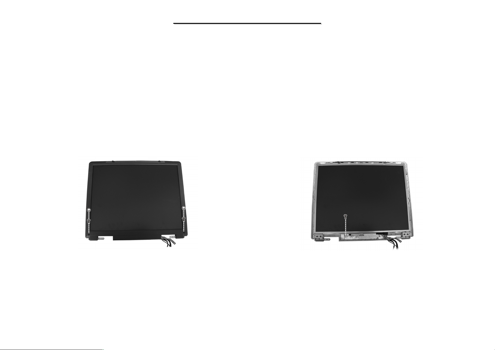
2. Remove two screws and rubbers on the corners of the LCD panel. (Figure 2-20)
3. Insert a flat screwdriver to the lower part of the LCD cover and gently pry the frame out. Repeat the process until
the cover is completely separated from the housing.
4. Remove the one screw fastening the inverter board. (Figure 2-21)
Figure 2-21 Remove the one screwFigure 2-20 Remove LCD cover
62
Page 64
8599
8599
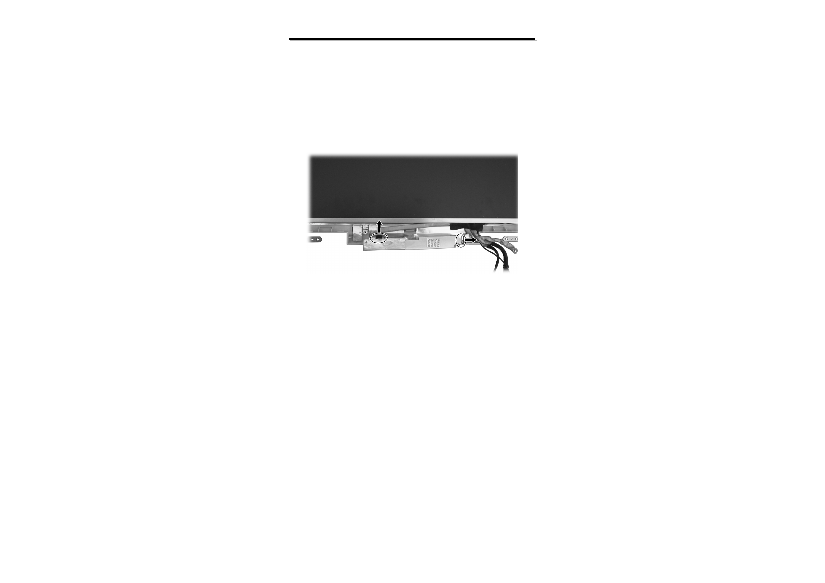
5. To remove the inverter board on the lower part of the LCD housing , disconnect two cables. (Figure 2-22)
N/B Maintenance
N/B Maintenance
Figure 2-22 Remove the inverter board
Reassembly
1. Reconnect the two cables. Fit the inverter board back into place and secure with one screw.
2. Replace the LCD cover and secure with two screws and rubbers.
3. Replace the LCD assembly. (Refer to section 2.2.8 Reassembly)
4. Replace the keyboard and battery pack. (Refer to sections 2.2.2 and 2.2.1 Reassembly)
63
Page 65
8599
8599
N/B Maintenance
N/B Maintenance
2.2.10 LCD Panel
Disassembly
1. Remove the battery, keyboard and LCD assembly. (Refer to sections 2.2.1, 2.2.2 and 2.2.8 Disassembly)
2. Remove the LCD cover. (Refer for two steps 2,3 of section 2.2.9 Disassembly)
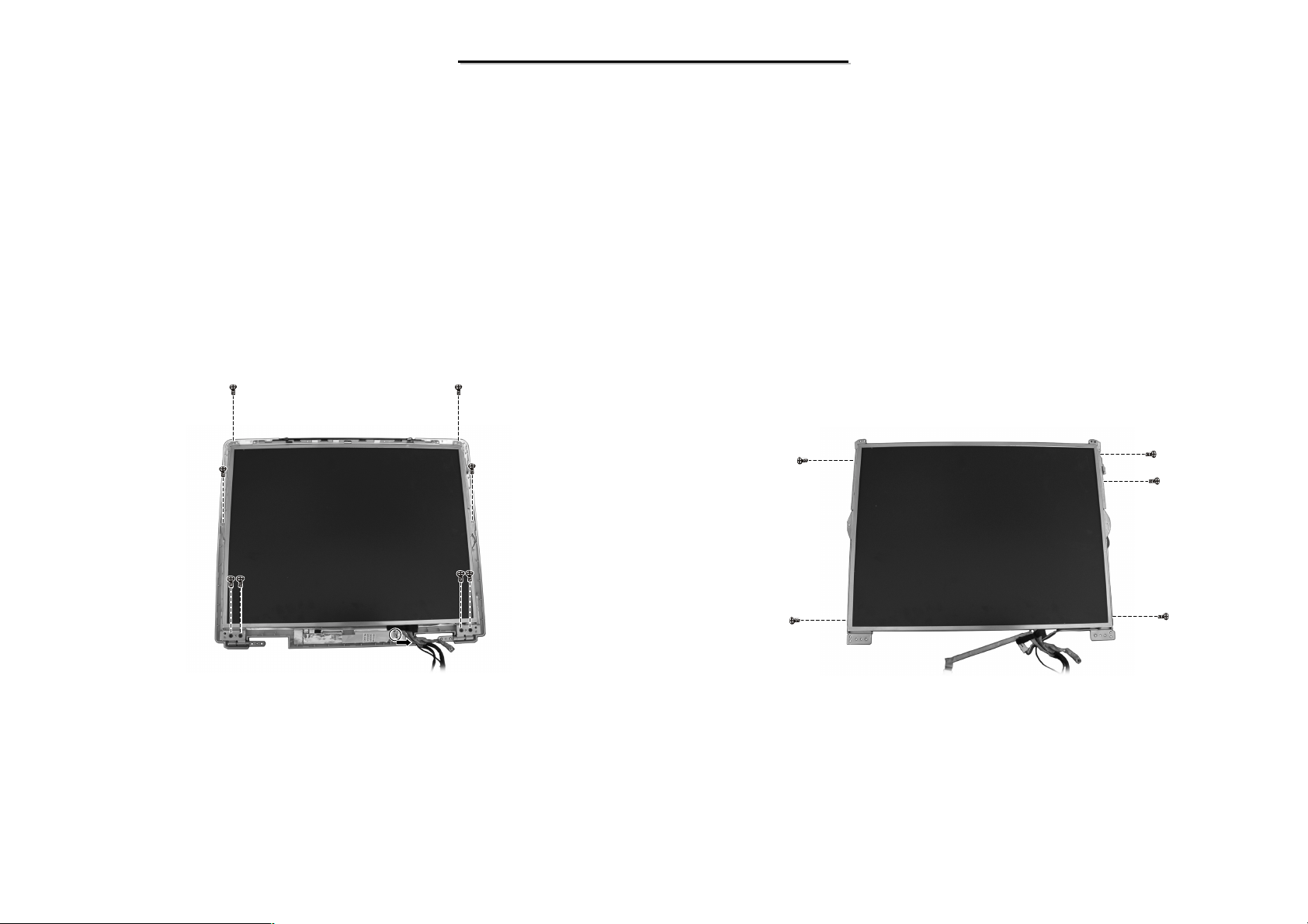
3. Remove the eight screws fastening the LCD panel and detach the cable, Then lift it up. (Figure 2-23)
4. Remove the five screws fastening the LCD brackets. (Figure 2-24)
Figure 2-23 Remove the eight screws
and detach the cable
Figure 2-24 Remove the five screws
64
Page 66
8599
8599
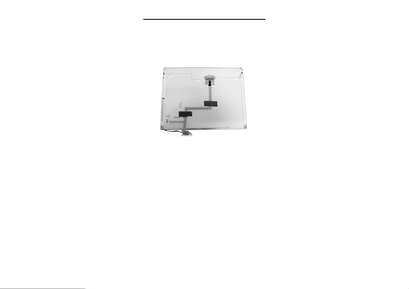
5. Disconnect the cable and free the LCD panel. (Figure 2-25)
N/B Maintenance
N/B Maintenance
Figure 2-25 Free the LCD panel
Reassembly
1. Reconnect the cable, then replace the LCD brackets and secure with five screws.
2. Fit the LCD panel back into place and secure with eight screws, then reconnect the cable to the inverter board.
3. Replace the LCD cover and secure with two screws and rubbers. (Refer to section 2.2.9 Reassembly)
4. Replace the LCD assembly. (Refer to section 2.2.8 Reassembly)
5. Replace the keyboard and battery pack. (Refer to sections 2.2.2 and 2.2.1 Reassembly)
65
Page 67
8599
8599
N/B Maintenance
N/B Maintenance
2.2.11 System Board
Disassembly
1. Remove the battery, keyboard, CPU, hard disk drive, CD/DVD-ROM drive, DIMM module, modem card and
LCD assembly. (Refer to sections 2.2.1, 2.2.2, 2.2.3, 2.2.4, 2.2.5, 2.2.6, 2.2.7 and 2.2.8 Disassembly)
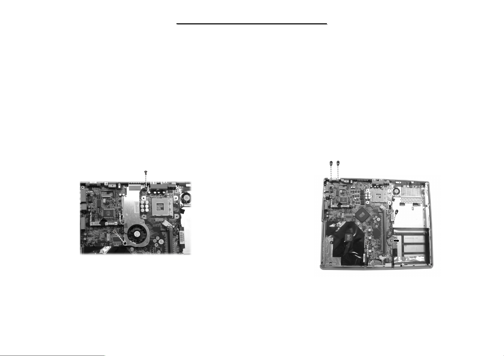
2. Disconnect the heatsink’s cable from the system board and remove two screws fastening the heatsink.
(Figure 2-26)
3. Disconnect the speaker’s cable and the touch pad’s cable from the system board.To free the system board, please
remove one screw and four hex nuts that fastening the system board. (Figure 2-27)
Figure 2-26 Free the heatsink
Figure 2-27 Free the system board
66
Page 68

8599
8599
Reassembly
1. Replace the system board into the top cover and secure with one screw and four hex nuts.
2. Reconnect the touch pad’s cable, the speaker’s cable.
3. Replace the heatsink and secure the two screws, then reconnect the cable to the system board.
4. Replace the modem card. (See sections 2.2.7 reassembly)
5. Replace the LCD assembly, DIMM module, CD/DVD-ROM, HDD, CPU, keyboard and battery pack. (See
sections 2.2.8, 2.2.6, 2.2.5, 2.2.4, 2.2.3, 2.2.2 and 2.2.1 Reassembly)
N/B Maintenance
N/B Maintenance
67
Page 69
8599
8599
N/B Maintenance
N/B Maintenance
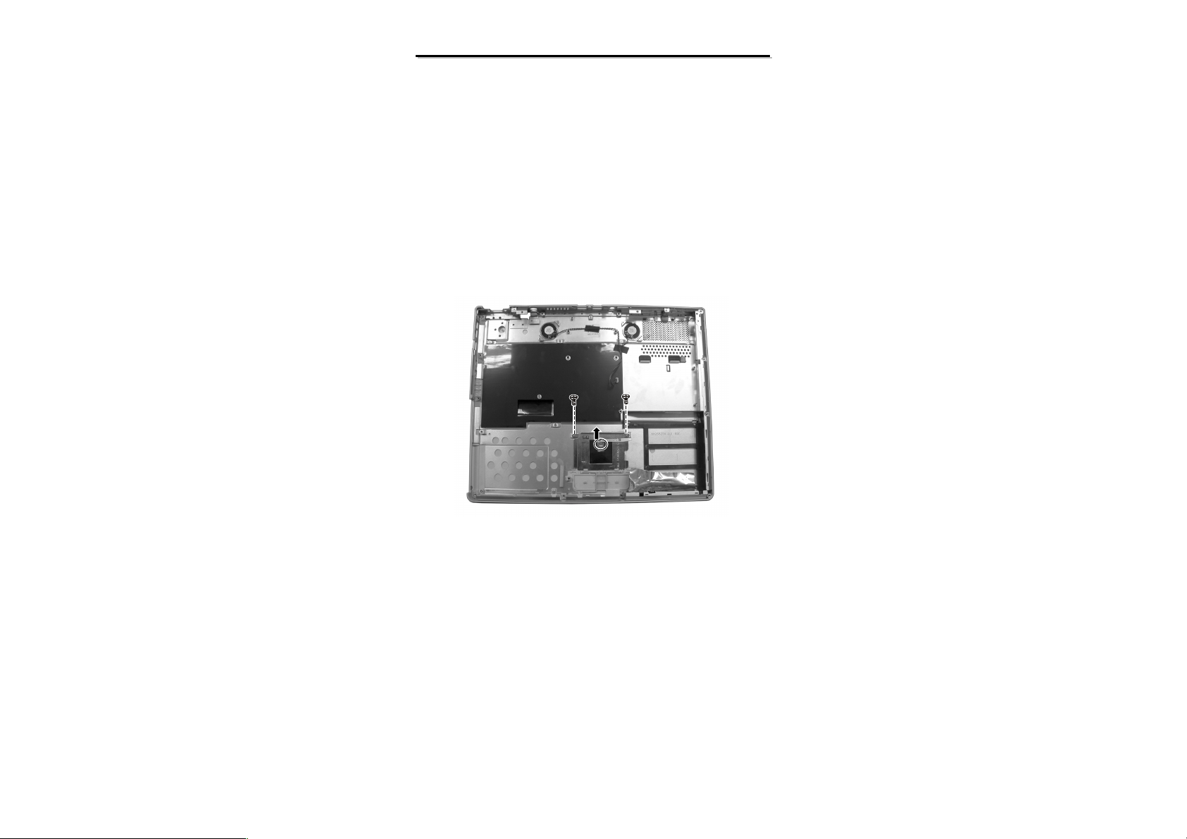
2.2.12 Touch Pad
Disassembly
1. Remove the system board. (See section 2.2.11 Disassembly)
2. Remove the two screws and disconnect the cable, then free the touch pad. (Figure 2-28)
Figure 2-28 Free the touch pad
Reassembly
1. Replace the touch pad and reconnect the cable.
2. Replace the touch pad shielding and secure with two screws.
3. Reassemble the notebook. (See the previous sections Reassembly)
68
Page 70
8599
8599
N/B Maintenance
N/B Maintenance
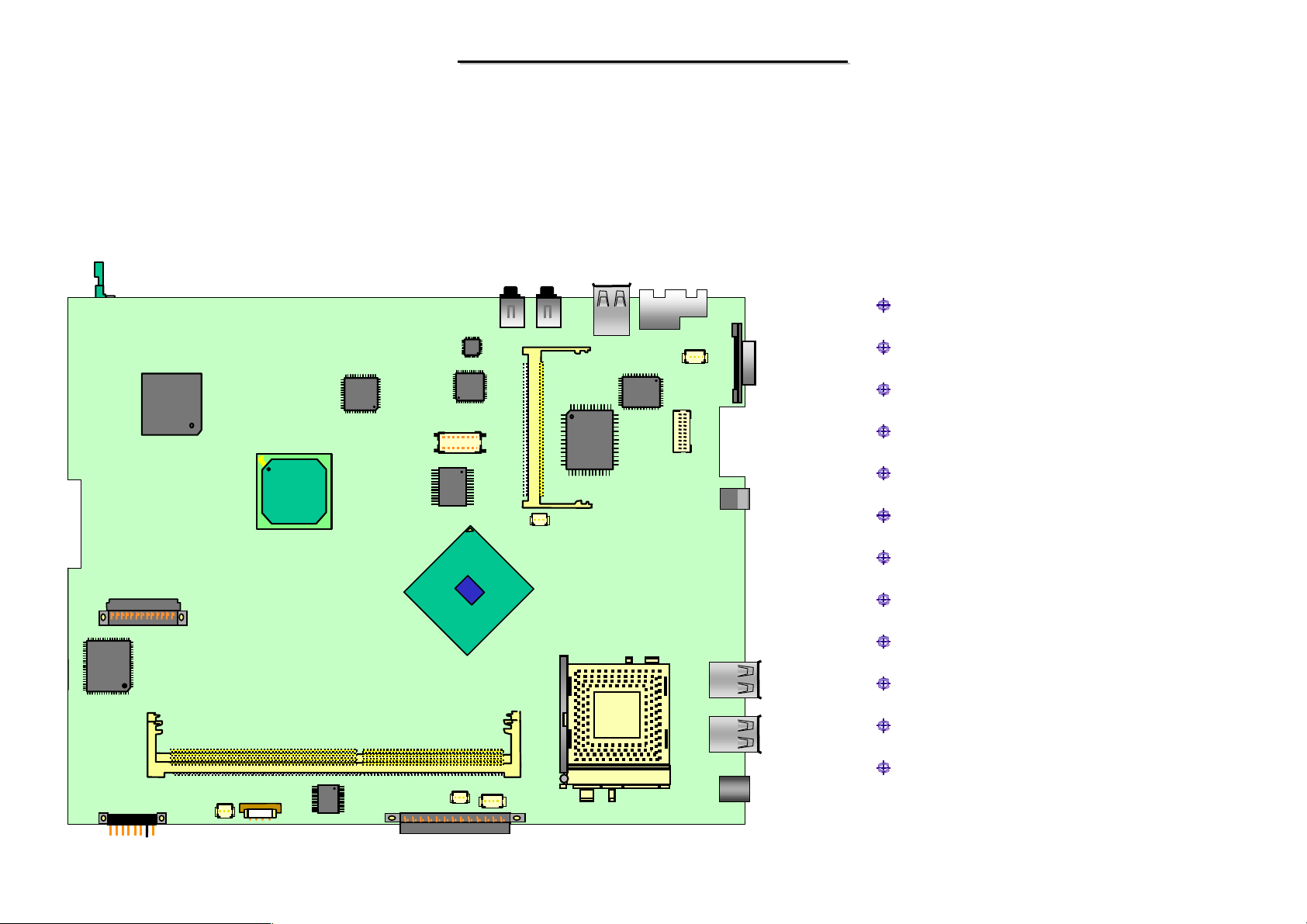
3. Definition & Location of Connectors / Switches
3.1 Mother Board (Side A) - 1
J9 J7
PJ1 : AC Power Jack
J509
J10
J13
J8
J12
J5
J6
J3
J4
J2
PJ2 : Battery Connector
J1 : S-Video Port
J2 : External VGA Connector
J3, J4, J9 : USB Port Connector
J1
J5 : MDC Jump Wire Connecto r
J6 : LCD Connector + Inverter
J7 : RJ11 & RJ45 Connect or
J8 : Internal Left Speak Connector
J10 : CPU Fan Connec tor
J12 : NB Fan Connector
J13 : Mini-PCI Socket
PJ1
------ To next page ------
PJ2
69
Page 71
8599
8599
N/B Maintenance
N/B Maintenance
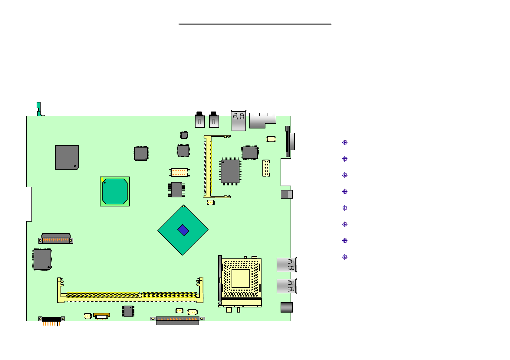
3. Definition & Location of Connectors / Switches
3.1 Mother Board (Side A) - 2
J14 J11
------ Continued to previous page ------
J11 : MIC In Jack
J21
J19
J509
J20
J18
J15
J14 : Line Out Jack
J15 : MDC Board Connector
J16 : Primary EIDE Connector
J18 : Extend DDR SDRAM Socket
J19 : RTC Battery Connector
J20 : Touch-Pad Connector
J21 : Secondary IDE Connector
J16
70
Page 72
8599
8599
N/B Maintenance
N/B Maintenance
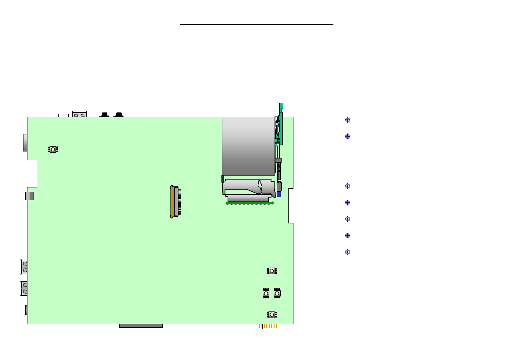
3. Definition & Location of Connectors / Switches
3.1 Mother Board (Side B)
J501 : Internal Keybo ard Connector
SW501
J501
J509
J502
SW503
SW502
SW504
J502 : PCMCIA Card Socket
SW501 : Power Button
SW502 : Touch-Pad Up Button
SW503 : Touch-Pad Right Button
SW504 : Touch-Pad Left Button
SW505 : Touch-Pad Down Button
SW505
71
Page 73
8599
8599
N/B Maintenance
N/B Maintenance
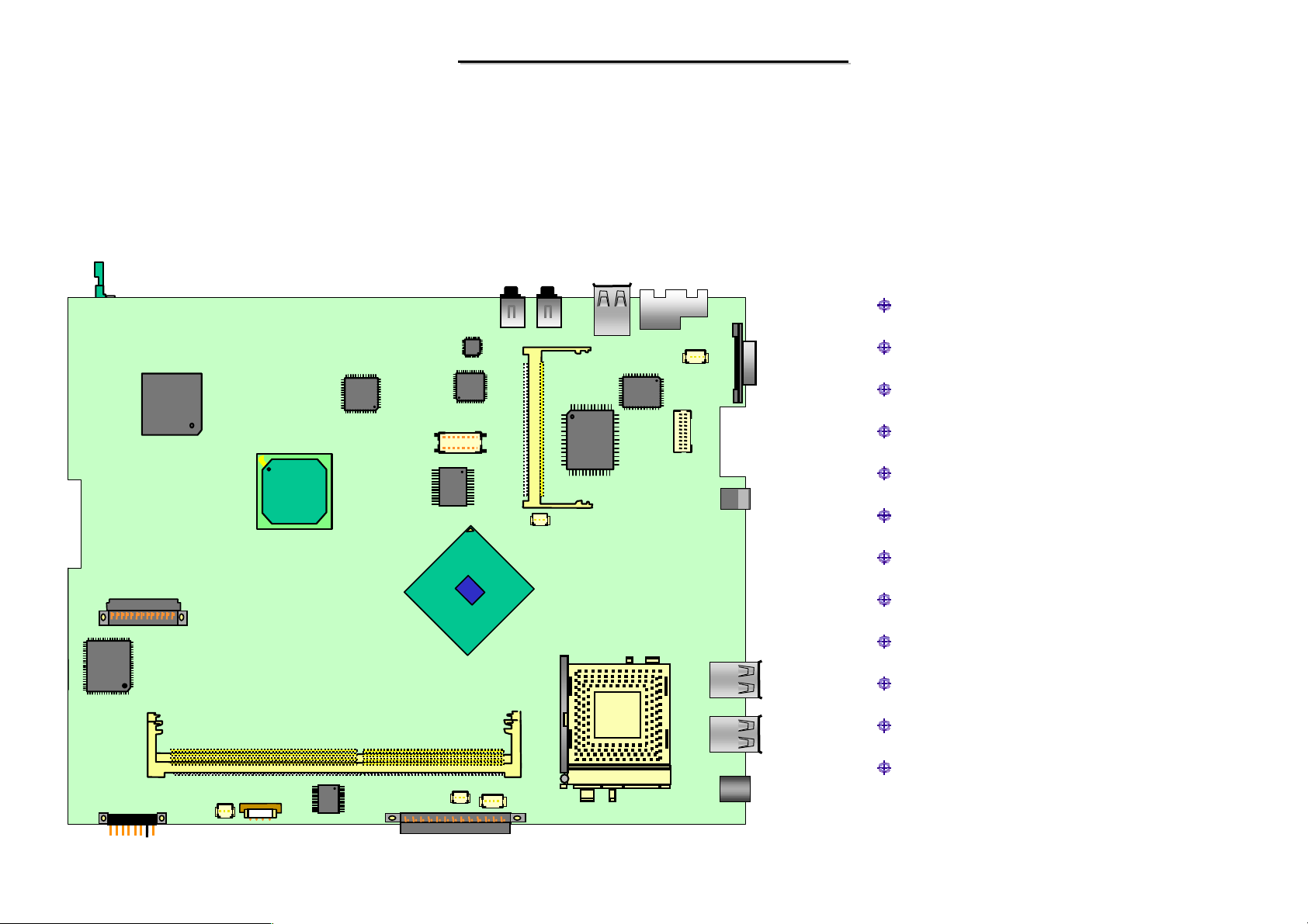
4. Definition & Location of Major Components
4.1 Mother Board (Side A)
U5 : ICS1883AF LAN Controller
U22
U23
J509
U20
U17
U19
U13
U10
U11
U12
U6
U5
U9
U6 : Intel P4 Proc ess Socket
U9 : TV/ LVDS Encoder (SiS301LV)
U10 : GMT G1422 Amplifer
U11 : VIA VI1616 Audio Codec
U12 : SiS M661FX NB
U13 : ICS952007 Clock Generator
U17 : KBC (W83L950D)
U19 : DDR Buffer Clock
U20 : SiS963L SB
U22 : Ti PCI1410A CardBus
U23 : LPC BIOS ROM
72
Page 74
8599
8599
N/B Maintenance
N/B Maintenance
5. Pin Descriptions of Major Components
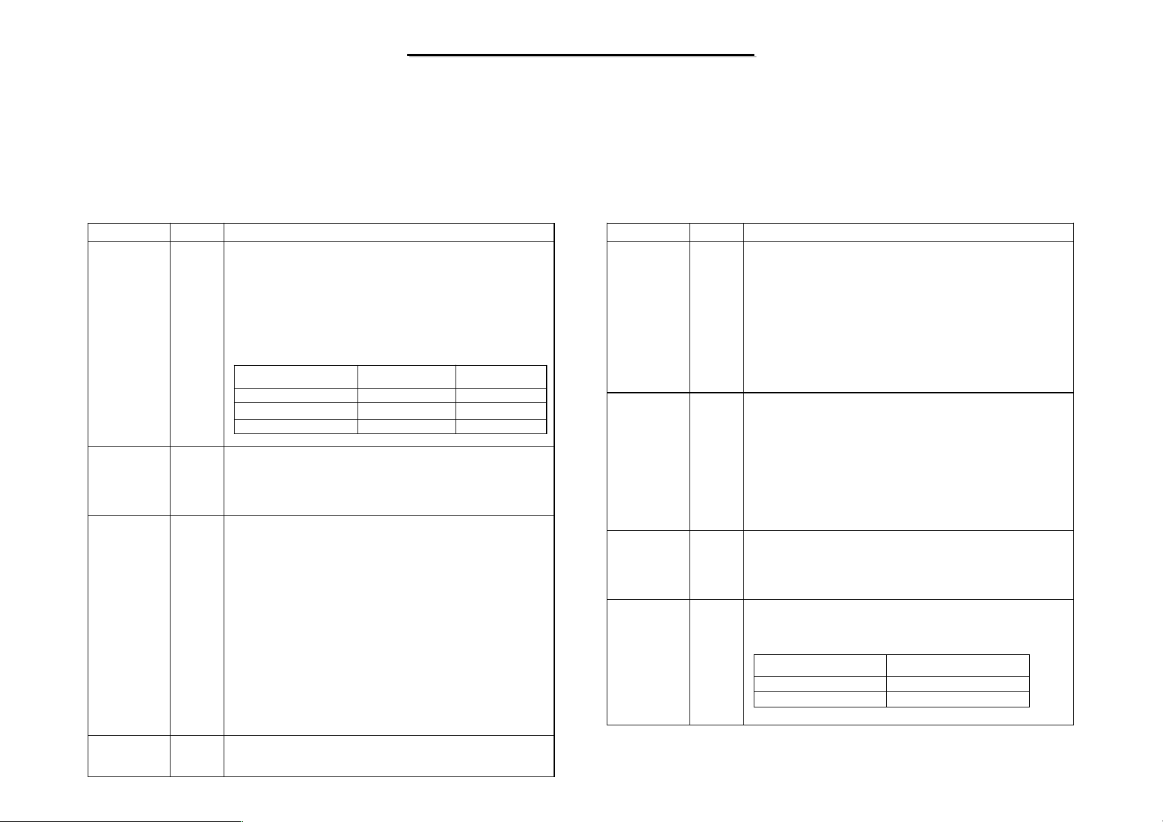
5.1 Intel Pentium 4 Processor mFC-PGA 478 Pins - 1
Name Type Description
AP[1:0]#
BCLK[1:0]
BINIT#
BNR#
Input/
Output
Input The differential pair BCLK (Bus Clock) determines the system bus
Input/
Output
Input/
Output
AP[1:0]# (Address Parity) are driven by the request initiator along
with ADS#,A[35:3]#, and the transaction type on the REQ[4:0]#. A
correct parity signal is high if an even number of covered signals
are low and low if an odd number of covered signals are low. This
allows parity to be high when all the covered signals are high.
AP[1:0]# should connect the appropriate pins of all Pentium 4
processor in the 478-pin package system bus agents. The following
table defines
Request Signals subphase 1 subphase 2
A[35:24]# AP0# AP1#
A[23:3]# AP1# AP0#
frequency. All processor system bus agents must receive these
signals to drive their outputs and latch their inputs.
All external timing parameters are specified with respect to the
rising edge of BCLK0 crossing V CROSS .
BINIT# (Bus Initialization) may be observed and driven by all
processor system bus agents and if used, must connect the
appropriate pins of all such agents. If the BINIT# driver is enabled
during power-on configuration, BINIT# is asserted
to signal any bus condition that prevents reliable future operation.
If BINIT# observation is enabled during power-on configuration,
and BINIT# is sampled asserted, symmetric agents reset their bus
LOCK# activity and bus request arbitration state machines. The bus
agents do not reset their IOQ and transaction tracking state
machines upon observation of BINIT# activation. Once the BINIT#
assertion has been observed, the bus agents will re-arbitrate for the
system bus and attempt completion of their bus queue and IOQ
entries.
If BINIT# observation is disabled during power-on configuration, a
central agent may handle an assertion of BINIT# as appropriate to
the error handling architecture of the system.
BNR# (Block Next Request) is used to assert a bus stall by any bus
agent who is unable to accept new bus transactions. During a bus
stall, the current bus owner cannot issue any new transactions.
REQ[4:0]# AP1# AP0#
Name Type Description
A[35:3]#
A20M#
ADS#
ADSTB[1:0]#
Input/
Output
Input If A20M# (Address-20 Mask) is asserted, the processor masks
Input/
Output
Input/
Output
A[35:3]# (Address) define a 2
space. In sub-phase 1 of the address phase, these pins transmit the
address of a transaction. In sub-phase 2, these pins transmit
transaction type information. These signals
must connect the appropriate pins of all agents on the Pentium 4
processor in the 478-pin package system bus. A[35:3]# are
protected by parity signals AP[1:0]#. A[35:3]# are source
synchronous signals and are latched into the receiving buffers by
ADSTB[1:0]#. On the active-to-inactive transition of RESET#, the
processor samples a subset of the A[35:3]# pins to determine
power-on configuration. See Section 7.1 for more details.
physical address bit 20 (A20#) before looking up a line in any
internal cache and before driving a read/write transaction on the
bus. Asserting A20M# emulates the 8086 processor's address
wrap-around at the 1-Mbyte boundary. Assertion of A20M# is only
supported in real mode.
A20M# is an asynchronous signal. However, to ensure recognition
of this signal following an Input/Output write instruction, it must be
valid along with the TRDY# assertion of the corresponding
Input/Output Write bus transaction.
ADS# (Address Strobe) is asserted to indicate the validity of the
transaction address on the A[35:3]# and REQ[4:0]# pins. All bus
agents observe the ADS# activation to begin parity checking,
protocol checking, address decode, internal snoop, or deferred reply
ID match operations associated with the new transaction.
Address strobes are used to latch A[35:3]# and REQ[4:0]# on their
rising and falling edges. Strobes are associated with signals as
shown below.
Signals Associated Strobe
REQ[4:0]#, A[16:3]# ADSTB0#
A[35:17]# ADSTB1#
-byte physical memory address
36
73
Page 75
8599
b
8599
N/B Maintenance
N/B Maintenance
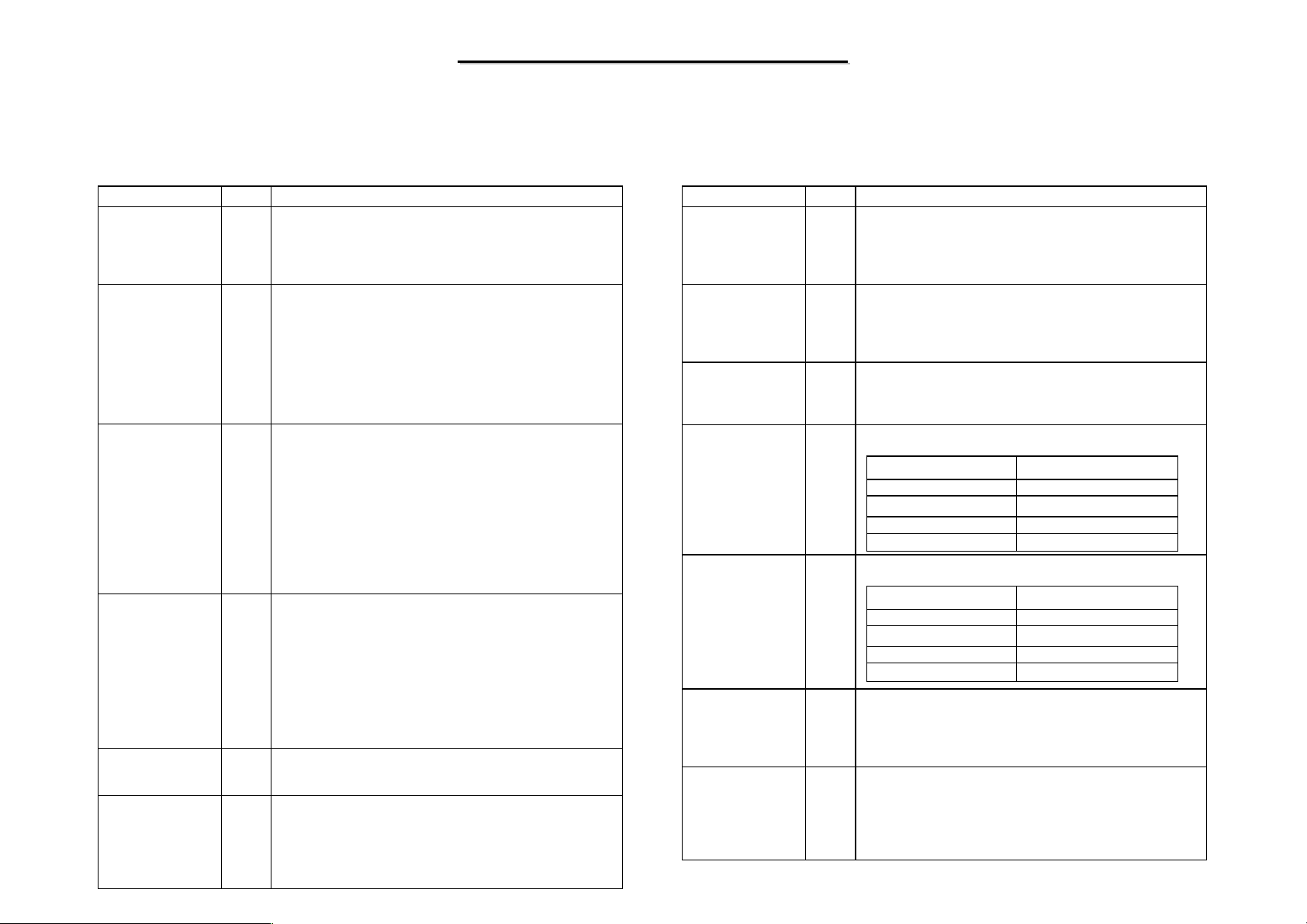
5.1 Intel Pentium 4 Processor mFC-PGA 478 Pins - 2
Name Type Description
HIT#
HITM#
IERR#
IGNNE#
INIT#
ITPCLKOUT[1:0]
ITP_CLK[1:0]
Input/
Output
Input/
Output
HIT# (Snoop Hit) and HITM# (Hit Modified) convey
transaction snoop operation results. Any system bus agent may
assert both HIT# and HITM# together to indicate that it requires
a snoop stall, which can be continued by reasserting
Output
HIT# and HITM# together.
Output IERR# (Internal Error) is asserted by a processor as the result of
an internal error. Assertion of IERR# is usually accompanied by
a SHUTDOWN transaction on the processor system bus. This
transaction may optionally be converted to an external error
signal (e.g., NMI) by system core logic. The processor will keep
IERR# asserted until the assertion of RESET#, BINIT#, or
INIT#.
This signals does not have on-die termination. Refer to
Section 2.5 fortermination requirements.
Input IGNNE# (Ignore Numeric Error) is asserted to force the
processor to ignore a numeric error and continue to execute
noncontrol floating-point instructions. If IGNNE# is deasserted,
the processor generates an exception on a noncontrol
floating-point instruction if a previous floating-point instruction
caused an error.IGNNE# has no effect when the NE bit in
control register 0 (CR0) is set. IGNNE# is an asynchronous
signal. However, to ensure recognition of this signal following
an Input/Output write instruction, it must be valid along with the
TRDY# assertion of the corresponding Input/Output Write bus
transaction.
Input INIT# (Initialization), when asserted, resets integer registers
inside the processor without affecting its internal caches or
floating-point registers. The processor then begins execution at
the power-on Reset vector configured during power-on
configuration. The processor continues to handle snoop requests
during INIT# assertion. INIT# is an asynchronous signal and
must connect the appropriate pins of all processor system bus
agents. If INIT# is sampled active on the active to inactive
transition of RESET#, then the processor executes its Built-in
Self-Test (BIST).
The ITPCLKOUT[1:0] pins do not provide any output for the
Pentium® 4 processor in the 478-pin package. Refer to Section
2.5 for additional details and termination requirements.
Input ITP_CLK[1:0] are copies of BCLK that are used only in
processor systems where no debug port is implemented on the
system board. ITP_CLK[1:0] are used as BCLK[1:0] references
for a debug port implemented on an interposer. If a debug port
is implemented in the system, ITP_CLK[1:0] are no connects in
the system. These are not processor signals.
Name Type Description
DBSY#
DEFER#
DP[3:0]#
DSTBN[3:0]#
DSTBP[3:0]#
FERR#
GTLREF
Input/
Output
Input
Input/
Output
Input/
Output
Input/
Output
Output FERR# (Floating-point Error) is asserted when the processor
DBSY# (Data Bus Busy) is asserted by the agent responsible for
driving data on the processor system bus to indicate that the data
us is in use. The data bus isreleased after DBSY# is deasserted.
This signal must connect the appropriate pins on all processor
system bus agents.
DEFER# is asserted by an agent to indicate that a transaction
cannot be guaranteed in-order completion. Assertion of
DEFER# is normally the responsibility of the addressed
memory or Input/Output agent. This signal must connect the
appropriate pins of all processor system bus agents.
DP[3:0]# (Data parity) provide parity protection for th e
D[63:0]# signals. They are driven by the agent responsible for
driving D[63:0]#, and must connect the appropriate pins of all
Pentium 4 processor in the 478-pin package system bus gents.
Data strobe used to latch in D[63:0]#.
Data strobe used to latch in D[63:0]#.
detects an unmasked floating-point error. FERR# is similar to
the ERROR# signal on the Intel 387 coprocessor, and is
included for compatibility with systems using MSDOS*-type
floating-point error reporting.
Input GTLREF determines the signal reference level for AGTL+ input
pins. GTLREF should be set at 2/3 V
AGTL+ receivers to determine if a signal is a logical 0 or
logica l 1 . R ef er t o the Intel® Pentium® 4 Processor in the
478-pin Package and Intel® 850 Chipset Platform Design
Guide for more information.
Signals Asso ci ated Strobe
D[15:0]#, DBI0# DSTBN0#
D[31:16]#, DBI1#
D[47:32]#, DBI2# DSTBN2#
D[63:48]#, DBI3# DSTBN3#
Signals Asso ci ated Strobe
D[15:0]#, DBI0# DSTBP0#
D[31:16]#, DBI1# DSTBP1#
D[47:32]#, DBI2# DSTBP2#
D[63:48]#, DBI3# DSTBP3#
DSTBN1#
. GTLREF is used by the
CC
74
Page 76
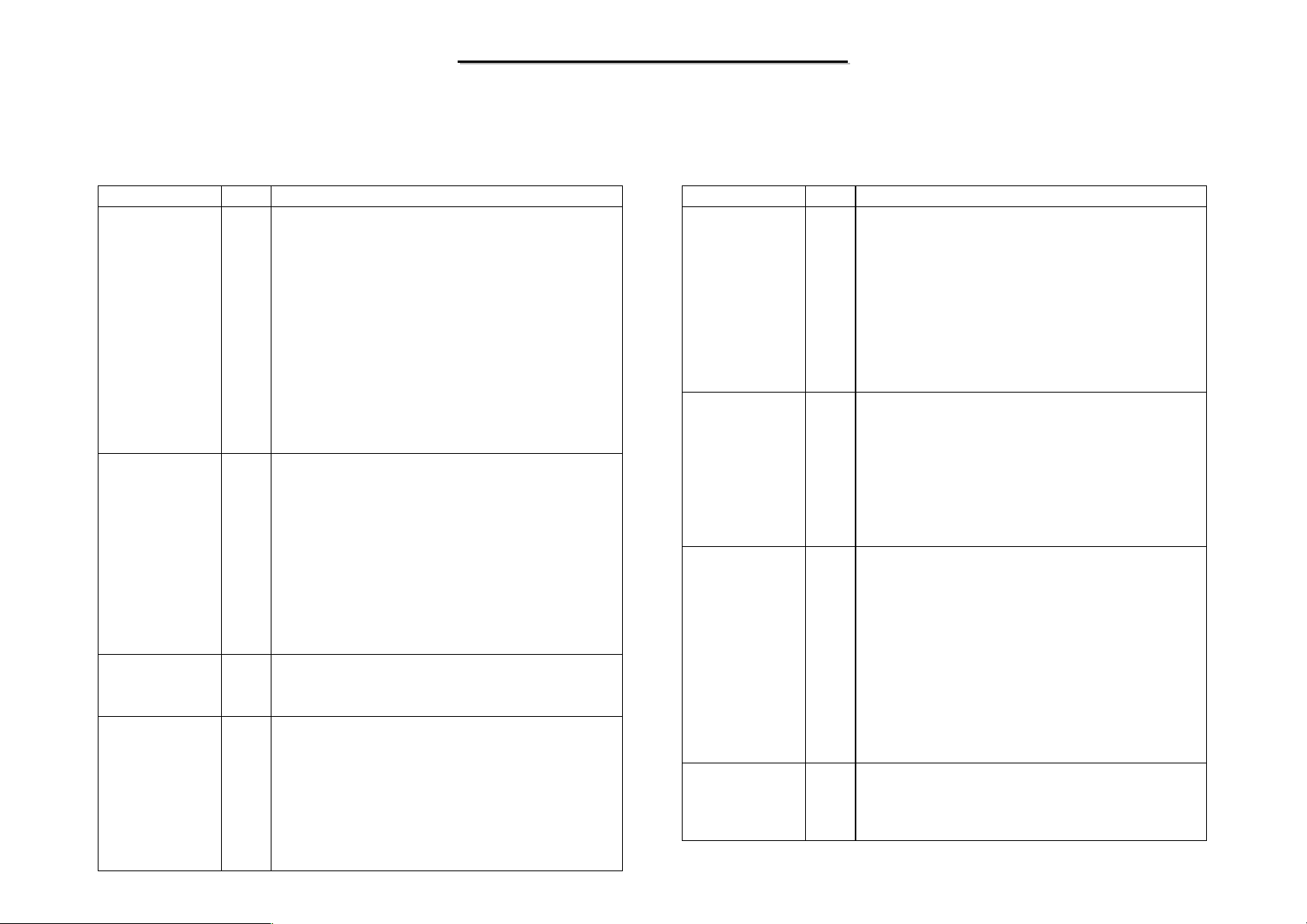
8599
8599
N/B Maintenance
N/B Maintenance
5.1 Intel Pentium 4 Processor mFC-PGA 478 Pins - 3
Name Type Description
PWRGOOD
RESET#
RS[2:0]#
RSP#
Input PWRGOOD (Power Good) is a processor input. The processor
requires this signal to be a clean indication that the clocks and
power supplies are stable and within their specifications.
‘Clean’ implies that the signal will remain low (capable of
sinking leakage current), without glitches, from the time that the
power supplies are turned on until they come within
specification. The signal must then transition monotonically to a
high state. Figure 11 illustrates the relationship of PWRGOOD
to the RESET# signal. PWRGOOD can be driven inactive at
any time, but clocks and power must again be stable before a
subsequent rising edge of PWRGOOD. It must also meet the
minimum pulse width specification in Table 16, and be followed
by a 1 to 10 ms RESET# pulse. The PWRGOOD signal must be
supplied to the processor; it is used to protect internal circuits
against voltage sequencing issues. It should be driven high
throughout boundary scan operation.
Input Asserting the RESET# signal resets the processor to a known
state and invalidates its internal caches without writing back any
of their contents. For a power-on Reset, RESET# must stay
active for at least one millisecond after VCC and BCLK have
reached their proper specifications. On observing active
RESET#, all system bus agents will deassert their outputs within
two clocks. RESET# must not be kept asserted for more than 10
ms while PWRGOOD is asserted.
A number of bus signals are sampled at the active-to-inactive
transition of RESET# for power-on configuration. These
configuration options are described in the Section 7.1.
This signal does not have on-die termination and must be
terminated on the system board.
Input RS[2:0]# (Response Status) are driven by the response agent
(the agent responsible for completion of the current transaction),
and must connect the appropriate pins of all processor system
bus agents.
Input RSP# (Response Parity) is driven by the response agent (the
agent responsible for completion of the current transaction)
during assertion of RS[2:0]#, the signals for which RSP#
provides parity protection. It must connect to the appropriate
pins of all processor system bus agents.
A correct parity signal is high if an even number of covered
signals are low and low if an odd number of covered signals are
low. While RS[2:0]# = 000, RSP# is also high, since this
indicates it is not being driven by any agent guaranteeing
correct parity.
Name Type Description
LINT[1:0]
LOCK#
MCERR#
PROCHOT#
Input
Input/
Output
Input/
Output
Output PROCHOT# will go active when the processor temperature
LINT[1:0] (Local APIC Interrupt) must connect the appropriate
pins of all APIC Bus agents. When the APIC is disabled, the
LINT0 signal becomes INTR, a maskable interrupt request
signal, and LINT1 becomes NMI, a nonmaskable interrupt.
INTR and NMI are backward compatible with the signals of
those names on the Pentium processor. Both signals are
asynchronous.
Both of these signals must be software configured via BIOS
programming of the APIC register space to be used either as
NMI/INTR or LINT[1:0]. Because the APIC is enabled by
default after Reset, operation of these pins as LINT[1:0] is the
default configuration.
LOCK# indicates to the system that a transaction must occur
atomically. This signal must connect the appropriate pins of all
processor system bus agent s. For a locked sequence of
transactions, LOCK# is asserted from the beginning of the
first transaction to the end of the last transaction.
When the priority agent asserts BPRI# to arbitrate for ownership
of the processor system bus, it will wait until it observes
LOCK# deasserted. This enables symmetric age nts to retain
ownership of the processor system bus throughout the bus
locked operation and ensure the atomicity of lock.
MCERR# (Machine Check Error) is asserted to indicate an
unrecoverable error without a bus protocol violation. It may be
driven by all processor system bus agents.
MCERR# assertion conditions are configurable at a system
level. Assertion options are defined by the following options:
Enabled or disabled.
Asserted, if configured, for internal errors along with IERR#.
Asserted, if configured, by the request initiator of a bus
transaction after it observes an error.
Asserted by any bus agent when it observes an error in a bus
transaction.
For more details regarding machine check architecture, please
refer to the IA-32 Software Develope r’s Manu a l, Volu me 3:
System Programming Guide.
monitoring sensor detects that the processor has reached its
maximum safe operating temperature.
This indicates that the processor Thermal Control Circuit has
been activated, if enabled. See Section 7.3 for more details.
75
Page 77
8599
p
8599
N/B Maintenance
N/B Maintenance
5.1 Intel Pentium 4 Processor mFC-PGA 478 Pins - 4
Name Type Description
REQ[4:0]#
SKTOCC#
SLP#
SMI#
STPCLK#
TCK
Input/
Output
Output SKTOCC# (Socket Occupied) will be pulled to ground by the
Input SLP# (Sleep ) , wh en a s s er ted in Sto p-Grant s t a te, cau s es t he
Input SMI# (System Management Interrupt) is asserted
Input STPCLK# (Stop Clock), when asserted, causes the processor to
Input TCK (Test Clock) provides the clock input for the processor
REQ[4:0]# (Request Command) must connect the appropriate
ins of all processor system bus agents. They are asserted by the
current bus owner to define the currently active transaction type.
These signals are source synchronous to ADSTB0#. Refer to the
AP[1:0]# signal description for a details on parity checking of
these signals.
proces s or. Sys t e m bo a r d de si g ners may use this pin to determine
if the processor is present.
proces s or t o en ter the Slee p s t a te. During Sleep st a te, the
processor stops providing internal clock signals to all units,
leaving only the Phase-Locked Loop (PLL) still operating.
Processors in this state will not recognize snoops or interrupts.
The processor will recognize only assertion of the RESET#
signal, deassertion of SLP#, and removal of the BCLK input
while in Sleep state. If SLP# is deasserted, the processor exits
Sleep state and returns to Stop-Grant state, restarting its internal
clock signals to the bus and processor core units. If the BCLK
input is stopped while in the Sleep state the processor will exit
the Sleep state and transition to the Deep Sleep state.
asynchronously by system logic. On accepting a System
Management Interrupt, the processor saves the current state and
enter System Management Mode (SMM). An SMI
Acknowledge transaction is issued, and the processor begins
program execution from the SMM handler.
If SMI# is asserted during the deassertion of RESET# the
processor will tristate its outputs.
enter a low power Stop-Grant state. The processor issues a
Stop-Grant Acknowledge transaction, and stops providing
internal clock signals to all processor core units except the
system bus and APIC units. The processor continues to snoop
bus transactions and service interrupts while in Stop-Grant state.
When STPCLK# is deasserted, the processor restarts its internal
clock to all units and resumes execution. The assertion of
STPCLK# has no effect on the bus clock; STPCLK# is an
asynchronous input.
Test Bus (also knownas the Test Access Port).
Name Type Description
TDI
TDO
TESTHI[12:8]
TESTHI[5:0]
THERMDA
THERMDC
THERMTRIP#
TMS
TRDY#
TRST#
VCCA
Input TDI (Test Data In) transfers serial test data into the processor.
TDI provides the serial input needed for JTAG specification
support.
Output TDO (Test Data Out) transfers serial test data out of the
processor. TDO provides the serial output needed for JTAG
specification support.
Input TESTHI[12:8] and TESTHI[5:0] must be connected to a VCC
power source through a resistor for proper processor operation.
See Section 2.5 for more details.
Other Thermal Diode Anode. See Section 7. 3. 1.
Other Thermal Diode Cathode. See Section 7.3.1.
Output Assertion of THERMTRIP# (Thermal Trip) indicates the
processor junction temperature has reached a level beyond
which permanent silicon damage may occur. Measurement of
the temperature is accomplished through an internal thermal
sensor which is configured to trip at approximately 135°C.Upon
assertion of THERMTRIP#, the processor will shut off its
internal clocks (thus halting program execution) in an attempt to
reduce the processor junction temperature. To protect the
processor, its core voltage (VCC) must be removed following
the assertion of THERMTRIP#. See Figure 12 and Table 16 for
the appropriate power down sequence and timing requirements.
Once activated, THERMTRIP# remains latched until RESET#
is asserted. While the assertion of the RESET# signal will
de-assert THERMTRIP# , if the processor’s junction
temperature remains at or above the trip level, THERMTRIP#
will again be asserted after RESET# is de-asserted.
Input TMS (Test Mod e Select) is a JTAG specification support signal
used by debug tools.
Input TRDY# (Target Ready) is asserted by the target to indicate that
it is ready to receive a write or implicit writeback data transfer.
TRDY# must connect the appropriate pins of all system bus
agents.
Input TRST# (Test Reset) resets the Test Access Port (TAP) logic.
TRST# must be dr iven low during power on Reset. This can be
done with a 680 . pull-down resistor.
Input VCCA provides isolated power for the internal processor core
PLLs. Refer to the Intel® Pentium® 4 Processor in the 478-pin
Package and Intel® 850 Chipset Platform Design Guide for
complete implementation details.
76
Page 78
8599
I
8599
N/B Maintenance
N/B Maintenance
5.1 Intel Pentium 4 Processor mFC-PGA 478 Pins - 5
Name Type Description
V
CCIOPLL
VCCSENSE
VCCVID
VID[4:0]
VSSA
VSSSENSE
TMS
TRDY#
TRST#
VCCA
Input
Output
Input
Output
Input V
Output
Input TMS (Test Mode Select) is a JTAG specification support signal
Input TRDY# (Target Ready) is asserted by the target to indicate that
Input TRST# (Test Reset) resets the Test Access Port (TAP) logic.
Input VCCA provides isolated power for the internal processor core
provides isolated power for internal processor system
V
CCIOPLL
bus PLLs. Follow he guidelines for V
Pentium® 4 Processor in the 478-pin Package and Intel® 850
Chipset Platfor m Design Gui de
details.
CCSENSE is an isolated low impedance connection to processor
V
core power(V
the silicon with little noise.
There is no imput voltage requirement for VCCVID for designs
intended tosupport only the Pentium 4 processor in the 478-pin
package. Refer to the
478-pin Package and Intel® 850 Chipset Platform Design
Guide
for more information.
VID[4:0] (Voltage ID) pins can be used to support automatic
selection of power supply voltages (Vcc). These pins are not
signals, but are either an open circuit or a short circuit to VSS
on the processor. The combination of opens and shorts
defines the voltage required by the processor. The VID pins are
needed t o c le a nly suppor t p rocessor voltage specifica t ion
variations. See Table 2 for definitions of these pins. The power
supply must supply the voltage that is requested by these pins,
or disable itself.
SSA is the isolated ground for internal PLLs.
V
SSSENSE is an isolated low impedance connectio n to processor
SS. It can be used to sense or measure ground near the
core V
silicon with little noise
used by debug tools.
it is ready to receive a write or implicit writeback data transfer.
TRDY# must connect the appropriate pins of all system bus
agents.
TRST# must be driven l ow during power on Reset. This can be
done with a 680 . pull-down resistor.
PLLs. Refer to the
Package and Intel® 850 Chipset Platform Design Guide
complete implementation details.
). It can be used to sense or measure power near
CC
Intel® Pentium® 4 Processor in the
Intel® Pent ium® 4 Proces sor in the 478-pin
, and refer to the
CCA
for complete implementation
ntel®
for
77
Page 79
8599
8599
N/B Maintenance
N/B Maintenance
5.2 SiS M661FX (IGUI Host Memory Controller) - 1
Host Bus Interface
Ball Name Ball Attr Description
CPUCLK
CPUCLK#
CPURST# O
CPUPWRGD O
ADS# I/O
HASTB[1:0]# I/O
HREQ[4:0]# I/O
HA[31:3]# I/O
BREQ0# O
BPRI# O
BNR# I/O
HLOCK# I
HIT# I/O
I
0.71V – M
0.9~1.8V – M
0.9~1.8V – M
0.9~1.8V – M
0.9~1.8V – M
0.9~1.8V – M
0.9~1.8V – M
0.9~1.8V – M
0.9~1.8V – M
0.9~1.8V – M
0.9~1.8V – M
0.9~1.8V – M
Host differential clock input.
Host Bus Reset:
CPURST# is used to keep all the bus agents in the
same initial state before valid cycles issued.
CPUPWRGD is used to inform CPU that main
power is stable
Address Strobe :
Address Strobe is driven by CPU or SiSM661FX
to indicate the start of a CPU bus cycle.
Source synchronous address strobe used to latch
HREQ[4:0]# & HA[31:3]# at both falling and
rising edge.
HREQ[4:0]# & HA[16:3]# are latched by
HASTB0# HA[31:17]# are latched by HASTB1#
Request Command:
HREQ[4:0]# are used to define each transaction
type during the clock when ADS# is asserted and
the clock after ADS# is asserted.
Host Address Bus
Symmetric Agent Bus Request:
BREQ0# is driven by the symmetric agent to
request for the bus.
Priority Agent Bus Request:
BPRI# is driven by the priority agent that wants to
request the bus.
BPRI# has higher priority than BREQ0# to access
a bus.
Block Next Request:
This signal can be driven asserted by any bus agent
to block further requests being pipeli n ed.
Host Lock :
CPU asserts HLOCK# to indicate the current bus
cycle is locked.
Keeping a Non-Modified Cache Line
Host Bus Interface (Continued)
Ball Name Ball Attr Description
HITM# I/O
0.9~1.8V – M
DEFER# O
0.9~1.8V – M
RS[2:0]# O
0.9~1.8V – M
HTRDY# O
0.9~1.8V – M
DRDY# I/O
0.9~1.8V – M
DBSY# I/O
0.9~1.8V – M
HD[63:0]# I/O
0.9~1.8V – M
DBI[3:0]# I/O
0.9~1.8V – M
Hits a Modified Cache Line:
Hit Modified indicates the snoop cycle hits a
modified line in the L1/L2 cache of CPU.
Defer Transaction Completion:
SiSM661FX will use this signal to indicate a retry
or defer response to host bus.
Response Status:
RS[2:0]# are driven by the response agent to
indicate the transaction response type. The
following shows the response type.
RS[2:0]# Response
000 Idle State
001 Retry
010 Defer
011 Reserved
100 Reserved
101 No data
110 Implicit Write-back
111 Normal
Target Ready:
During write cycles, response agent will drive
TRDY# to indicate it is ready to accept data.
Data Ready:
DRDY# is driven by the bus owner whenever the
data is valid on the bus.
Data Bus Busy:
Whenever the data is not valid on the bus with
DRDY# is deserted, DBSY# deasserted to hold the
bus.
Host Data Bus
Dynamic Bus Inversion: An active DBI# will
invert it’s corresponding data group signals.
DBI0# is referenced by HD[15:0]#
DBI1# is re fe renced by HD[ 31:16]#
DBI2# is re fe renced by HD[ 47:32]#
DBI3# is re fe renced by HD[ 63:48]#
78
Page 80
8599
8599
N/B Maintenance
N/B Maintenance
5.2 SiS M661FX (IGUI Host Memory Controller) - 2
Host Bus Interface (Continued)
Ball Name Ball Attr Description
HDSTBP[3:0]# I/O
HDSTBN[3:0]# I/O
HCOMP_N I
HCOMP_P I
HVREF[4:0]
HCOMPVREF_N
0.9~1.8V – M
0.9~1.8V– M
M
M
I
M
Source synchronous data strobe used to latch data
at falling edge
HD[15:0]#, DBI0# are latched by HDSTBP0#
HD[31:16]#, DBI1# are latched by HDSTBP1#
HD[47:32]#, DBI2# are latched by HDSTBP2#
HD[63:48]#, DBI3# are latched by HDSTBP3#
Source synchronous data strobe used to latch data
at falling edge
HD[15:0]#, DBI0# are latched by HDSTBN0#
HD[31:16]#, DBI1# are latched by HDSTBN1#
HD[47:32]#, DBI2# are latched by HDSTBN2#
HD[63:48]#, DBI3# are latched by HDSTBN3#
GTL N-MOS Com p ensati o n Input
GTL P- MOS Compensation Input
AGTL+ I/O reference voltage
MuTIOL® 1G Interface
Pin Name Pin Attr Description
ZCLK I
3.3V - M
ZUREQ/ZDREQ I/O
1.8V - M
ZSTB[1:0] I/O
1.8V - M
ZSTB[1:0]# I/O
1.8V - M
ZAD[16:0] I/O
1.8V - M
ZVREF I
M
ZCMP_N I
M
ZCMP_P I
M
SiS MuTIOL ? ?1G clock
SiS MuTIOL ? ?1G Control pins
SiS MuTIOL ? ?1G Strobe
Strobe Compliment
Address/Data/DBI Pins
SiS MuTIOL ? ?1G Reference Voltage
N-MOS Compensation Input
P-MOS Compensation Input
DRAM Controller
Ball Name Ball Attr Description
DRAMTEST I
2.5V - M
FWDSDCLKO O
2.5V – M
MA[14:0] O
2.5V - M
SRAS# O
2.5V - M
SCAS# O
2.5V - M
SWE# O
2.5V - M
CS[5:0]# O
2.5V - M
DQM#[7:0] O
2.5V - M
DQS[7:0] I/O
2.5V - M
MD[63:0] I/O
2.5V - M
CKE[5:0] O
2.5V – AUX
S3AUXSW# O (open-drain)
2.5V - AUX
DDRVREF[A:B] I M DDR I/O Reference Voltage
DDRCOMP_P I
M
DDRCOMP_N I
M
Test Clock Input
SDRAM Forward Clock Output
System Memory Address Bus
SDRAM Row Address Strobe
SDRAM Column Address Strobe
SDRAM Write Enable
SDRAM Chip Select
CS[5:0]# multiplexed with DQS[5:0]
SDRAM Input/Output Data Mask
2.5V - M DDR Data Strobe
System Memory Data Bus
SDRAM Clock Enable
Aux power swi t ch for ACPI-S3 state, lo w ac tive.
P-MOS Compensation Input
N-MOS Compensation Input
79
Page 81
8599
8599
N/B Maintenance
N/B Maintenance
5.2 SiS M661FX (IGUI Host Memory Controller) - 3
AGP Interface
Ball Name Ball Attr Description
AGPCLK I
3.3V – M
AFRAME# I/O
1.5V - M
AIRDY# I/O
1.5V - M
ATRDY# I/O
1.5V - M
ASTOP# I/O
1.5V - M
ADEVSEL# I/O
1.5V - M
ASERR# I
1.5V - M
AREQ# I
1.5V - M
AGNT# O
1.5V - M
ADBI_LO I/O
1.5V - M
AAD[31:0] I/O
1.5V - M
AC/BE[3:0]# I/O
1.5V - M
APAR I/O
1.5V - M
ST[2:0] O
1.5V - M
PIPE# I
1.5V - M
SBA[7:0] I/O
1.5V - M
RBF# I
1.5V - M
WBF# I
1.5V - M
AGP Clock
AGP Frame#
AGP Initiator Ready
AGP Target Ready
AGP Stop#
AGP Device Select
AGP System Error
AGP Bus Request
AGP Bus Grant
DBI of AAD[15:0]
AGP Address/Data Bus
AGP Command/Byte Enable
AGP Parity
AGP Status Bus
AGP Pipeline Request in v2.0
DBI of AAD[31:16] in v3.0
Side Band Address
Read Buffer Full
Write Buffer Full
AGP Interface (Continued)
Ball Name Ball Attr Description
AD_STB[1:0] I/O
1.5V - M
AD_STB[1:0]# I/O
1.5V - M
SB_STB I
1.5V - M
SB_STB# I
1.5V - M
GC_DET# I
1.5V - M
AGPCOMP_P I
M
AGPCOMP_N I
M
AGPVREF I
M
AD Bus Strobe
AD Bus Strobe Compliment
Side Band Strobe
Side Band Strobe Compliment
AGP v3.0 strap
P-MOS Compensation Input
N-MOS Compensation Input
AGP Reference Voltage
Stereo Glasses interface
Ball Name Ball Attr Description
CSYNC O
3.3V - M
RSYNC O
3.3V - M
LSYNC O
3.3V - M
Reserved
Reserved
Reserved
80
Page 82
8599
8599
N/B Maintenance
N/B Maintenance
5.2 SiS M661FX (IGUI Host Memory Controller) - 4
Digital Video Link Interface
Ball Name Ball Attr Description
VBCLK I
1.8V - M
VBHCLK O
1.8V - M
VBCAD I/O
1.8V - M
VBCTL[1:0] O
1.8V -M
VGPIO[3:2] I/O
1.8V - M
VBHSYNC I/O
1.8V - M
VBVSYNC I/O
1.8V - M
VBDE I/O
1.8V - M
VBGCLK I/O
1.8V - M
VBGCLK# I/O
1.8V - M
VBD[11:0] I/O
1.8V - M
VAHSYNC I/O
1.8V - M
VAVSYNC I/O
1.8V - M
VADE I/O
1.8V - M
VAGCLK I/O
1.8V - M
VAGCLK# I/O
1.8V - M
VAD[11:0] I/O
1.8V - M
Channel B/A Clock Input
VBCLK multiplexed with SBA0
VB Programming Interface Clock
VBHCLK multiplexed with RBF#
VB Programming Interface Data
VBCAD multiplexed with AREQ#
VB Data Control
VBCTL[1:0] multiplexed with AAD[29:28]
VB GPIO pins
VGPIO[3:2] multiplexed with IPE#/WBF#
Channel B H-Sync
VBHSYNC multiplexed with AAD30
Channel B V-Sync
VBVSYNC multiplexed with AAD31
Channel B Data Valid
VBDE multiplexed with AAD27
Channel B Clock Output.
This clock is used to trigger dual edge data
transfer. Perfect duty cycle is required.
VBGCLK multiplexed with AD_STB1
Channel B Differential Clock Output. (To support
Chrontel).
VBGCLK# multiplexed with AD_STB1#
Channel B Data
VBD[11:0] multiplexed with AAD
Channel A H-Sync
VAHSYNC multiplexed with AAD18
Channel A V-Sync
VAVSYNC multiplexed with AAD17
Channel A Data Valid
VADE multiplexed with AAD16
Channel A Clock Output.
This clock is used to trigger dual edge data 1.8V –
M transfer. Perfect duty cycle is required.
VAGCLK multiplexed with A D_STB0
Channel A Differential Clock Output. (To support
Chrontel).
VAGCLK# multiplexed with AD_STB0#
Channel A Data
VAD[11:0] mu l t iplexed wi t h AAD
Test Mode / Hardware Trap / Power Management
Ball Name Ball Attr Description
DLLEN# I/O
3.3V/5V– M
TRAP2 I
3.3V/5V– AUX
TRAP[1:0] I
3.3V/5V– M
ENTEST I
3.3V/5V– M
TESTMODE[2:0] I
3.3V/5V– M
AUXOK I
3.3V – AUXI
PCIRST# I
3.3V – AUXI
PWROK I
3.3V – AUXI
Hardware Trap pin (refer to section 5)
Hardware Trap pin (refer to section 5)
Hardware Trap pins (refer to section 5)
Test Mode enable pin
Test Mode select pin
Nand Tree Test: 100
Auxiliary Power OK :
This signal is supplied from the power source of
resume well. It is also used to reset the logic in
resume power well. If there is no auxiliary power
source on the system, this pin should be tied
together
with PWROK.
PCI Bus Reset :
PCIRST# is supplied from SiS963 MuTIOL ? ?1G
Media IO.
Main Power OK :
A high-level input to this signal indicates the
power being supplied to the system is in stable
operating state. During the period of PWROK
being low, CPURST and PCIRST# will all be
asserted until after PWROK goes high for 24 ms.
81
Page 83
5.2 SiS M661FX (IGUI Host Memory Controller) - 5
VGA interface
Ball Name Ball Attr Description
VOSCI I
3.3V - M
HSYNC O
3.3V – M
VSYNC O
3.3V - M
INTA# O
3.3V – M
VGPIO[1:0] I/O
3.3V/5V- M
VCOMP AI
Analog - M
VRSET AI
Analog - M
VVBWN AI
Analog - M
ROUT AO
Analog - M
GOUT AO
Analog - M
BOUT AO
Analog - M
14.318MHzReference Clock Input
Horizontal Sync
Vertical Sync
Internal VGA Interrupt Pin
Internal VGA GPIO pins
Compensation Pin
Reference Resistor
Voltage Reference
Red Signal Output
Green Signal Output
Blue Signal Output
8599
8599
N/B Maintenance
N/B Maintenance
82
Page 84
8599
8599
N/B Maintenance
N/B Maintenance
5.3 SiS963L(MuTIOL®Media I/O South Bridge) - 1
Host Bus Interface
Name Pin Attr Description
FERR#
IGNNE#
NMI
INTR
APICD1 /
GPIOFF#
APICD0 /
THERM2#
CPUSLP#
STPCLK#
SMI#
INIT#
APICCK/
LDTREQ# /
AGPBUSY#
A20M#
I
0.8V/2.65V -M
OD
0.8V/2.65V -M
OD
0.8V/2.65V -M
OD
0.8V/2.65V -M
I/OD
I
I/OD
I
0.8V/2.65V -M
OD
0.8V/2.65V -M
OD
0.8V/2.65V -M
OD
0.8V/2.65V -M
OD
0.8V/2.65V -M
I
2.5V/3.3V -M
OD
0.8V/2.65V- M
Floating Point Error: CPU will assert this signal upon
a floating point error occurring.
Ignore Numeric Error: IGNNE# is asserted to inform
CPU to ignore a numeric error.
Non-Maskable Interrupt: A rising edge on NMI will
trigger a non-maskable interrupt to CPU.
Interrupt Request:
conveys to CPU that there is outstanding interrupt(s)
needed to be serviced.
APIC Dat a: APICD[ 1 : 0]
These two signals are used to send and receive APIC
data.
GPIO OFF: Turn off the system when input a low level
signal.
Thermal 2: Assert a SMI#/SCI# when input a low level
signal.
CPU Sleep: The CPUSLP# can be used to force CPU
enter the Sleep state.
Stop Clock: STPCLK# will be asserted to inhibit or
throttle CPU activities upon a pre-defined
power management event occurs.
System Management Interrupt: SMI# will be asserted
when a pre-defined power management event occurs.
Initialization:
flushing its internal caches and registers. In Pentium III
platform it is active high. This signal requires an external
pull-up resistor tied to VTT.
APIC Clock: This signal is used to determine when
valid data is being sent over the APCI bus.
LDTREQ# / AGPBUSY# (LDTREQ# for K8 use
only)
When a low active signal inputs, it will wake up system
from C3/S1.
Address 20 Mask: When A20M# is asserted, the CPU
A20 signal will be forced to “0”
High-level voltage of this signal
INIT is used to re-start the CPU without
MuTIOL 1G Connect Interface
Name Pin Attr Description
ZCLK
ZUREQ
ZDREQ
ZSTB[1:0]
ZSTB[1:0]#
ZAD[16:0]
ZVREF
ZCMP_N
ZCMP_P
I
3.3V - M
I/O
1.8V - M
I/O
1.8V - M
I/O
1.8V - M
I/O
1.8V - M
I/O
1.8V - M
I -M MuTIOL 1G I/O reference voltage
I -M MuTIOL 1G N-MOS Compensation Input
I -M MuTIOL 1G P-MOS Compensation input
MuTIOL 1G I/O Connect Clock
MuTIOL 1G I/O Conect Controll pins
MuTIOL 1G I/O Conect Controll pins
MuTIOL 1G I/O Connect Strobe
MuTIOL 1G Strobe Compliment
MuTIOL 1G Address/Data pins
LPC Interface
Name Pin Attr Description
LAD[3:0]
LDRQ#
LDRQ1#
(GPIO1)
LFRAME#
SIRQ
I/O
3.3V/5V-M
I
3.3V/5V-M
I
3.3V/5V-M
O
3.3V -M
I/O
3.3V/5V -M
LPC Address/Data Bus:
LPC cont ro ll er dr ives these fo ur pins t o t ransmit LPC
command, address, and data to LPC device.
LPC DMA Request 0:
This pin is used by LPC device to request DMA cycle.
LPC DMA Request 1:
This pin is used by LPC device to request DMA cycle.
LPC Frame:
This pin is used to notify LPC device that a start or a
abort LPC cycle will occur.
Serial IRQ:
This signal is used as the serial IRQ line signal.
83
Page 85
8599
p
8599
N/B Maintenance
N/B Maintenance
5.3 SiS963L(MuTIOL®Media I/O South Bridge) - 2
PCI Interface
Name Pin Attr Description
PCICLK
C/BE[3:0]#
PLOCK#
AD[31:0]
PAR
IRDY#
I
3.3V/5V -M
I/O
3.3V/5V -M
I/O
3.3V/5V -M
I/O
3.3V/5V -M
I/O
3.3V/5V -M
I/O
3.3V/5V -M
PCI Clock: The PCICLK input provides the
fundamental timing and the internal operating
frequency for the SiS963L. It runs at the same frequency
and skew of the PCI
local bus.
PCI Bus Command and Byte Enables: PCI Bus
Command and Byte Enables define the PCI command
during the address phase of a PCI cycle, and the PCI
byte enables during the data phases.
C/BE[3:0]# are outputs when the SiS963L is a PCI bus
master and inputs when it is a PCI slave.
PCI Lock: When PLOCK# is sampled asserted at the
beginning of a PCI cycle, SiS963L considers itself being
locked and remains in the locked state until PLOCK# is
sampled and negated at the following PCI cycle.
PCI Address /Data Bus: In address phase:
1.When the SiS963L is a PCI bus master, AD[31:0] are
output signals.
2.When the SiS963L is a PCI target, AD[31:0] are input
signals. In data phase:
1.When the SiS963L is a target of a memory read/write
cycle, AD[31:0] are floating.
2.When the SiS963L is a target of a configuration or an
I/O cycle, AD[31:0] are output signals in a read cycle,
and input signals in a write cycle.
Parity: SiS963L drives out Even Parity covering
AD[31:0] and C/BE[3:0]#. It does not check the input
parity signal.
Initiator Ready: IRDY# is an output when the SiS963L
is a PCI bus master. The assertion of
IRDY# indicates the current PCI bus master's ability to
complete the current data phase of the transaction. For a
read cycle, IRDY# indicates that the PCI bus master is
prepared to accept the read data on the following rising
edge of the PCI clock. For a write cycle, IRDY#
indicates that the bus master has driven valid data on the
PCI bus. When the SiS963L is a PCI slave, IRDY# is an
input pin.
PCI Interface (Continued)
Name Pin Attr Description
FRAME#
TRDY#
STOP#
DEVSEL#
PREQ[4:0]#
PGNT[4:0]#
PREQ5# /
GPIO5
I/O
3.3V/5V -M
I/O
3.3V/5V -M
I/O
3.3V/5V -M
I/O
3.3V/5V -M
I
3.3V/5V -M
O
3.3V –M
I
I/O
3.3V/5V- M
Frame#:FRAME# is an output when the SiS963L is a
PCI bus master. The SiS963L drives FRAME# to
indicate the beginning and duration of a n access. When
the SiS963L is a PCI slave device, FRAME# is an input
signal.
Target Ready: TRDY# is an output when the SiS963L
is a PCI slave. The assertion of TRDY#
indicates the target agent's ability to complete the current
data phase of the transaction. For a read cycle, TRDY#
indicates that the target has driven valid data onto the
PCI bus. For a write cycle, TRDY# indicates that the
target is
the SiS963L is a P C I master, it is an input pin.
Stop#:STOP# indicates that the bus master must start
terminating its current PCI bus cycle at the next clock
edge and release control of the PCI bus. STOP# is used
for disconnection, retry, and target-abortion sequences
on the PCI bus.
Device Select: As a PCI target, SiS963L asserts
DEVSEL# by doing positive or subtractive
decoding. SiS963L positively asserts DEVSEL# when
the DRAM address is being accessed by a PCI master,
PCI configuration registers or embedded controllers’
registers are being addressed, or the BIOS memory
space is being accessed. The low 16K I/O space and low
16M memory space are responded subtractively. The
DEVESEL# is an input pin when SiS963L is acting as a
PCI master. It is asserted by the addressed agent to claim
the current transaction.
PCI Bus Request:
PCI Bus Master Request Signals
PCI Bus Grant:
PCI Bus Master Grant Signals
PCI Bus Request:
PCI Bus Master Request Signal
repared to accept data from the PCI bus. When
84
Page 86
8599
8599
N/B Maintenance
N/B Maintenance
5.3 SiS963L(MuTIOL®Media I/O South Bridge) - 3
PCI Interface (Continued)
Name Pin Attr Description
PGNT5# /
GPIO6
INT[A:D]#
PCIRST#
SERR#
O
I/O
3.3V- M
I
3.3V/5V –M
O
3.3V –M
I
3.3V/5V –M
PCI Bus Grant:
PCI Bus Master Grant Signal
PCI interrupt A,B,C,D:
The PCI interrupts will be connected to the inputs of the
internal Interrupt controller through the rerouting logic
associated with each PCI interrupt.
PCI Bus Reset:
PCIRST# will be asserted during the period when
PWROK is low, and will be kept on asserting until about
24ms a f t er PWROK goes hig h.
System Error:
When sampled active low, a non-maskable interrupt
(NMI) can be generated to CPU if enabled.
Keyboard Controller Interface
Name Pin Attr Description
KBDAT
(GPIO15)
KBCLK
(GPIO16)
PMDAT
(GPIO17)
PMCLK
(GPIO18)
I/OD
3.3V/5V -AUX
I/OD
3.3V/5V -AUX
I/OD
3.3V/5V -AUX
I/OD
3.3V/5V -AUX
Keyboard Dada:
When the internal keyboard controller is enabled, this
pin is used as the keyboard data signal.
Keyboard Clock:
When the internal keyboard controller is enabled, this
pin is used as the keyboard clock signal.
PS2 Mouse Data:
When the internal keyboard and PS2 mouse controllers
are enabled, this pin is used as PS2 mouse data signal.
PS2 Mouse Clock:
When the internal keyboard and PS2 mouse controllers
are enabled, this pin is used as the PS2 mouse clock
signal.
IDE Interface
Name Pin Attr Description
IDA[15:0]
IDB[15:0]
IDECSA[1:0]#
IDECSB[1:0]#
IIOR[A:B]#
IIOW[A:B]#
ICHRDY[A:B]
IDREQ[A:B]
IDACK[A:B]#
IIRQ[A:B]
IDSAA[2:0]
IDSAB[2:0]
CBLID[A:B]
I/O
3.3V/5V -M
I/O
3.3V/5V -M
O
3.3V -M
O
3.3V -M
O
3.3V -M
O
3.3V -M
I
3.3V/5V -M
I
3.3V/5V -M
O
3.3V -M
I
3.3V/5V -M
O
3.3V -M
O
3.3V -M
I
3.3V/5V -M
Primary Channel Data Bus
Secondary Channel Data Bus
Primary Channel CS[1:0]
Secondary Channel CS[1:0]
Primary/Secondary Channel IOR# Signals
Primary/Secondary Channel IOW# Signals
Primary/Secondary Channel ICHRDY# Signals
Primary/Secondary Channel DMA Request Signals
Primary/Secondary Channel DMACK# Signals
Primary/Secondary Channel Interrupt Signals
Primar y Channel Address [2:0]
Secondary Channel Address [2:0]
Primary/Secondary Ultra-66 Cable ID
85
Page 87
8599
8599
N/B Maintenance
N/B Maintenance
5.3 SiS963L(MuTIOL®Media I/O South Bridge) - 4
Power Management Interface
Name Pin Attr Description
ACPILED
EXTSMI#
(GPIO3)
PME#
PSON#
AUXOK
PWRBTN#
THERM#
(GPIO2)
EXTSMI#
(GPIO3)
CLKRUN#
(GPIO4)
OD
<=5V -AUX
I
I/O
3.3V/5V -M
I
3.3V/5V -AUX
OD
<=5V -AUX
I
3.3V -AUX
I
3.3V/5V -AUX
I
3.3V/5V -M
I
3.3V/5V -M
I/O
3.3V/5V –M
ACPILED :
ACPILED can be used to control the blinking of an LED
at the frequency of 1 Hz
to indicate the system is at power saving mode.
External SMI#:
EXTSMI# can be used to generate wakeup event, sleep
event, or SCI/SMI# event to the ACPI compatible power
management unit.
PME# :
When the system is in power-down mode, an active low
event on PME# will cause the PSON# to go low and
hence turn on the power supply. When the system is in
suspend mode, an active PME# event will cause the
system wakeup and generate an SCI/SMI#.
ATX Power ON/OFF control:
PSON# is used to control the on/off state of the ATX
power supply. When the ATX power supply is in the
OFF state, an activated power-on event will force the
power supply to ON state.
Auxiliary Power OK:
This signal is supplied from the AUX power source. It is
also used to reset the logic in AUX power well. If there
is no auxiliary power source on the system, this pin
should be tied together with PWROK.
Power Button:
This signal is from the power button switch and will be
monitored by the ACPI-compatible power management
unit to switch the system between working and sleeping
states.
Thermal Alarm:
When a low active signal inputs, it will assert a
SMI#/SCI# event and assert CPU throttling.
External SMI#:
EXTSMI# can be used to generate wakeup event, sleep
event, or SCI/SMI# event to the ACPI compatible
power management unit.
Clock Run: (for Mobile only)
Used by PCI and LPC peripherals to request the system
PCI clock to re-start, or prevent PCI clock stopping. An
external pull-up to the MAIN power is required.
Power Management Interface (Continued)
Name Pin Attr Description
GPWAK#
(GPIO7)
RING
(GPIO8)
AC_SDIN2, 3
(GPIO9, 10)
STP_PCI# /
AGPSTOP#
(GPIO11)
CPUSTP#
(GPIO12)
DPRSLPVR
(GPIO13)
AGPSTOP# /
S3AUXSW#
(GPIO14)
I
3.3V/5V -AUX
I
3.3V/5V -AUX
I
3.3V/5V -AUX
O
OD
3.3V/5V –AUX
OD
1.5V/5V -AUX
O
3.3V/5V -AUX
OD
3.3V/5V -AUX
General Purpose Wake-Up Signal:
Used to wake up the system from S1/S3/S4/S5.
Ring Indication:
An active RING pulse and lasting for more than 4ms
will cause a wakeup event for system to wake from
S1~S5.
AUDIO Wake-Up Signal:
Used to wake up the system from S1/S3/S4/S5.
Stop PCI Clock: (for Mobile only) Used to stop the
system PCI clock. Used to support PCI CLKRUN#
protocol. AGP Clock Stop: (for Mobile only, if
GPIO14 is used to be S3AUXSW#)
AGPSTOP# is used to stop the AGP_CLOCK output
from clock generator during C3/S1 state.
CPU Clock Stop (for Mobile only):
For Intel Mobile processor, this signal can be used to
stop the clock to the processor.
This signal connected to the DPSLP# signal of Pentium
4 processor that can let the processor enter the Deep
Sleep state as well (recommended). For AMD processor,
this signal can be to reduce processor voltage during
C3/S1 state.
Deeper Sleep (for Mobile only):
Used to lower the voltage of VRM during CPU entered
the deeper power saving mode. Because this signal will
be at input mode after the Clear RTC operation, an
external pulled down resistor is required for this signal.
When this signal is high, the voltage regulator outputs
the Deepe r S leep voltage.
When this signal is low (default), the voltage regulator
output the Normal voltage. DPRSLP# can be used to
lower the Intel processor voltage during C3/S1 state.
AGP Clock Stop (for Mobile only):
AGPSTOP# is used to stop the AGP_CLOCK output
from clock generator during C3/S1 state.
S3AUXSW#:(for SiS755 and SiSR658 use only) The
signal will keep low in S3 state.
86
Page 88
8599
8599
N/B Maintenance
N/B Maintenance
5.3 SiS963L(MuTIOL®Media I/O South Bridge) - 5
Power Management Interface (Continued)
Name Pin Attr Description
VR_HILO#
(GPIO15)
LO_HI#
(GPIO16)
VGATEM#
(GPIO17)
RTC32KHZ
(GPIO18)
THERM2#
(APICD0)
GPIOFF#
(APICD1)
O
3.3V/5V -AUX
OD
1.5V/5V -AUX
OD
1.5V/5V -AUX
O
3.3V/5V -AUX
I
0.8V/2.65V -M
I
0.8V/2.65V -M
Voltage Regulator HI / LO (for Mobile only):
This ping is used to select an appropriate VID for
voltage regulator.
A low level indicates the Battery Optimal mode. A high
level indicates the Maximum Performance mode.
LO_HI# (for Mobile only):
This pin is connected to the processor. A high level
indicates the Battery Optimal mode. A low level
indicates the Maximum Performance mode.
VGATEM# (for Mobile only):
Output pin, it is used to mask the PWRGOOD of
processor core voltage regulator.
RTC32KHz output: (Mobile only)
Support RTC32KHz clock output in S0~S5.
Thermal Alarm2: (GTL level)
When a low active signal inputs, it will assert a
SMI#/SCI# event.
GPIO OFF: (GTL level)
When a low level signal inputs, it will turn off the
system. Then, the system can only be woken up again by
PWRBTN#.
General Purpose I/O
Name Pin Attr Description
GPIO[6:0]
GPIO[15:7]
GPIO[18:16]
GPIO[20:19]
GPIO[24:21]
I/O
3.3V/5V -M
I/O
3.3V/5V - AUX
O
3.3V/5V – AUX
OD
3.3V/5V – AUX
I
3.3V/5V - AUX
GPIO:
Can be a General Purpose Input or Output.
GPIO:
Can be a General Purpose Input or Output.
GPO:
Can be a General Purpose Output.
GPIO:
Can be a General Purpose Input or Output.
GPI:
Can be a General Purpose Input.
RTC Interface
Name Pin Attr Description
BATOK
OSC32KHI
OSC32KHO
PWROK
I
3.3V -RTC
I
3.3V-RTC
O
3.3V -RTC
I
3.3V-RTC
Battery Power OK:
When the internal RTC is enabled, this signal is used to
indicate that the power of RTC well is stable. It is also
used to reset the logic in RTC well. If the internal
RTC is disabled, this pin shou ld be tied low.
RTC 32.768 KHz Input:
When internal RTC is enabled, this pin provides the
32.768 KHz clock signal from external crystal or
oscillator.
RTC 32.768 KHz Output:
When internal RTC is enabled, this pin should be
connected with the other end of the 32.768 KHz crystal
or left unconnected if an external oscillator is used.
Main Power OK:
A high-level input to this signal indicates the power
being supplied to the system is in stable operating state.
During the period of PWROK being low, PCIRST# will
all be asserted until after PWROK goes high for 12 ms.
Hardware Trap Signals
Name Pin Attr Description
IPB_OUT0
IPB_OUT1
O
3.3V -AUX
O
3.3V – AUX
IPB_OUTO:
Hardware Trap to select MuTIOL 1G clock PLL
enable/disable
IPB_OUT1:
Hardware Trap to select MuTIOL 1G operation mode
87
Page 89
8599
8599
N/B Maintenance
N/B Maintenance
5.3 SiS963L(MuTIOL®Media I/O South Bridge) - 6
AC’97 Interface
Name Pin Attr Description
AC_BIT_CLK
AC_RESET#
AC_SDIN0
AC_SDIN1
AC_SDIN[3:2]
(GPIO[10:9])
AC_SDOUT
AC_SYNC
I
3.3V/5V -M
O
3.3V -AUX
I
3.3V/5V -AUX
I
3.3V/5V -AUX
I
3.3V/5V -AUX
O
3.3V -M
O
3.3V -M
AC’97 Bit Clock:
This signal is a 12.288MHz serial data clock, which is
generated by primary Codec.
AC’97 Reset:
Hardware reset signal for external Codecs.
AC’97 Serial Data Input :
Serial data input from primary Codec.
AC’97 Serial Data Input:
Serial data input from secondary Codec. When Modem
Codec is used, this pin dedicate to Modem Serial data
input.
AC’97 Serial Data Input:
Serial data input from third and forth Audio Codec.
AC’97 Serial Data Output:
Serial data output to Codecs.
AC’97 Synchronization:
This is a 48KHz signal, which is used to synchronize the
Codecs.
Legacy I/O and Miscellaneous Signals
Name Pin Attr Description
SPK
ENTEST
OSCI
O
3.3V -M
I
3.3V/5V -M
I
3.3V -M
Speaker output:
The SPK is connected to the system speaker.
SiS963L Test Mode Enable Pin
14.318 MHz. Clock In
USB Interface
Name Pin Attr Description
OSC12MHI
OSC12MHO
USBCLK48M
OC[0:5]#
UV[3,0]+,
UV[3,0]-
UV[4,1]+,
UV[4,1]-
UV[5,2]+,
UV[5,2]-
USBREF
I
3.3V/5V -AUX
O
3.3V/5V -AUX
I
3.3V/5V -M
I/O
3.3V/5V - AUX
I/O
3.3V - AUX
I/O
3.3V - AUX
I/O
3.3V - AUX
I
3.3V – AUX
UTMI 12MHz Clock Input:
This pin provides the 12MH z clock signal inpu t form
external crystal or oscillator.
UTMI 12Mhz Clock Output:
This pin should be connected with the other end of
the 12Mhz crystal or left unconnected if an external
oscillator is used
USB 48 MHz clock input:
This signal provides the fundamental clock for the USB
Controller.
USB Port 0-5 Overcurrent Detection:
OC[0:5]# are used to detect the overcurrent condition of
USB Ports 0-5.
USB Port [3:0] Differential:
These di ff er ential p airs are us e d t o tr ansmi t
Data/Address /Command signals for ports 3 and 0. (USB
controller 0)
USB Port [4:1] Differential:
These di ff er ential p airs are us e d t o tr ansmi t
Data/Address/Command signals for ports 4 and 1. (USB
controller 1)
USB Port [5,2] Differentia
These differential pairs are used to transmit
Data/Address/Command signals for ports 5 and 2. (USB
controller 2)
USB reference resistor input:
A resistor should be connected to USBVSS from this pin
for IO impedance calibration.
l:
88
Page 90
8599
8599
6. System Block Diagram
N/B Maintenance
N/B Maintenance
U6
Pentium 4
Prescott/Northwood
Processor
FSB 800MHz
Mini-PCI Socket
Type III A
Ti PCI1410A
PCMCIA &
Card Reader
U21
Power Switch
PCMCIA/CARDBUS
U22
Socket
CRT
TFT LCD
S-VIDEO
USB2.0 * 6
CDROM
Cover Switch
HDD
U9
TV-Encoder
SiS301LV
PCI Interface
Fan1/Fan2
Power Button
Touch Pad
U12
North Bridge
SiS M661FX
MuTIOL
interface
1GHz
U20
South Bridge
SiS963L
U17
W83L950D
KBC
Memory Bus 266/333/400MHz
U5
LAN PHY
AC Link
LPC Interface
U23
BIOS
PLCC 32
M.D.C
U11
Audio Codec
Amplifier
U10
184 pin DDR SO-DIMM Socket * 2
RJ-45 Jack
Cable
Cable
RJ-11 Jack
External
Microphone
Internal
Speaker
External
Speaker
Keyboard
89
Page 91

8599
8599
7. Maintenance Diagnostics
7.1 Introduction
Each time the computer is turned on, the system bios runs a series of internal checks on the hardware. This power-
on self test (post) allows the computer to detect problems as early as the power-on stage. Error messages of post
can alert you to the problems of your computer.
If an error is detected during these tests, you will see an error message displayed on the screen. If the error occurs
before the display is initialized,then the screen cannot display the error message. Error codes or system beeps are
used to identify a post error that occurs when the screen is not available.
N/B Maintenance
N/B Maintenance
The value for the diagnostic port (378H) is written at the beginning of the test. Therefore, if the test failed, the user
can determine where the problem occurred by reading the last value written to port 378H by the 378H port debug
board plug at Mini PCI Slot.
90
Page 92
7.2 Error Codes (1)
Following is a list of error codes in sequent displ ay on the PIO debug board.
8599
8599
N/B Maintenance
N/B Maintenance
POST Routine DescriptionCode
Some type of lone reset10h
Turn off FAST A20 for POST11h
Signal power on reset12h
Initialize the chipset13h
Search for ISA Bus VGA adapter14h
Reset counter / Timer 115h
User register config through CMOS16h
Size memory17h
Dispatch to RAM test18h
Check sum the ROM19h
Reset PIC’s1Ah
Initialize video adapter(s)1Bh
POST Routine DescriptionCode
Test keyboard20h
Test keyboard controller21h
Check if CMOS RAM valid22h
Test battery fail & CMOS X-SUM23h
Test the DMA controller24h
Initialize 8237A controller25h
Initialize int vectors26h
RAM quick sizing27h
Protected mode entered safely28h
RAM test completed29h
Protected mode exit successful2Ah
Setup shadow2Bh
Initialize video (6845Regs)1Ch
Initialize color adapter1Dh
Initialize monochrome adapter1Eh
Test 8237A page registers1Fh
Going to initialize video2Ch
Search for monochrome adapter2Dh
Search for color adapter2Eh
Sign on messages displayed2Fh
91
Page 93
7.2 Error Codes (2)
Following is a list of error codes in sequent displ ay on the PIO debug board.
8599
8599
N/B Maintenance
N/B Maintenance
POST Routine DescriptionCode
Special init of keyboard ctlr30h
Test if keyboard Present31h
Test keyboard Interrupt32h
Test keyboard command byte33h
Test, blank and count all RAM34h
Protected mode entered safely(2)35h
RAM test complete36h
Protected mode exit successful37h
Update output port38h
Setup cache controller39h
Test if 18.2Hz periodic working3Ah
Test for RTC ticking3Bh
POST Routine DescriptionCode
Configure the COMM and LPT ports40h
Initialize the floppies41h
Initialize the hard disk42h
Initialize option ROMs43h
OEM’s init of power management44h
Update NUMLOCK status45h
Test for coprocessor installed46h
OEM functions before boot47h
Dispatch to operate system boot48h
Jump into bootstrap code49h
ACPI init50h
PM init & Geyserville CPU init51h
Initialize the hardware vectors3Ch
Search and init the mouse3Dh
Update NUMLOCK status3Eh
Special init of COMM and LPT ports3Fh
USB HC init52h
92
Page 94
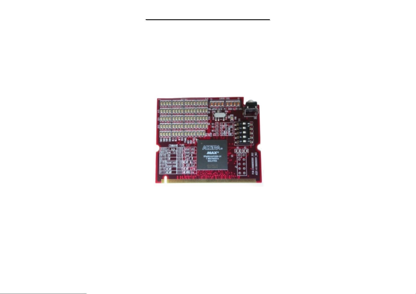
8599
8599
N/B Maintenance
N/B Maintenance
7.3 Debug Tool
7.3.1 Diagnostic Tool for Mini PCI Slot :
P/N:411906900001
Description: PWA-MPDOG;MINI PCI DOGKELLER CARD
Note: Order it from MIC/TSSC
93
Page 95

8. Trouble Shooting
8599
8599
N/B Maintenance
N/B Maintenance
8.1 No Power (*1)
8.2 Battery Can not Be Charged
8.3 No Display (*2)
8.4 LCD No Display or Picture Abnormal
8.5 External Monitor No Display or Color Abnormal
8.6 TV Test Error
8.9 Hard Drive Test Error
8.10 CD-ROM Driver Test Error
8.11 USB Port Test Error
8.12 PC Card Socket Test Error
8.13 Mini-PCI Socket Test Error
8.14 Audio Failure
8.7 Memory Test Error
8.8 Keyboard (K/B) Touch-Pad (T/P) Test Error
8.15 LAN Test Error
94
Page 96

8599
8599
N/B Maintenance
N/B Maintenance
*1: No power definition
Base on ACPI Spec. We define the no power as while we press the power button, the system can’t leave S5 status
or none the PG signal send out from power supply.
Judge condition:
Check whether there are any voltage feedback control to turn off the power.
Check whether no CPU power will cause system can’t leave S5 status.
If there are not any diagram match these condition, we should stop analyzing the schematic in power supply sending
out the PG signal. If yes, we should add the effected analysis into no power chapter.
*2: No display definition
Base on the digital IC three basic working conditions: working power, reset, Clock. We define the no display as
while system leave S5 status but can’t get into S0 status.
Judge condition:
Check which power will cause no display.
Check which reset signal will cause no display.
Check which Clock signal will cause no display
Base on these three conditions to analyze the schematic and edit the no display chapter.
Keyword:
S5: Soft Off
S0: Working
For detail please refer the ACPI specification
95
Page 97
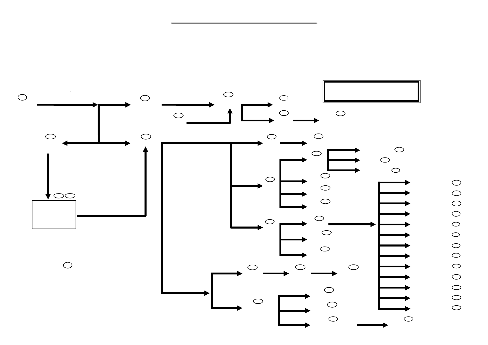
8.1 No Power (1)
When power button is pressed ,nothing happens ,power indicator does not light up.
8599
8599
N/B Maintenance
N/B Maintenance
P23
Power In
PJ1
PU22
PU23
PD7
PQ43
PQ42
PL19
PR136
PF1,PL1,PL2
PL6,PD4
P23
ADINP
CHARGE
BATT
NOTE :
P22
PQ7
PQ8
P24
PQ38,PQ39,PQ36
DISCHARGE
: Page 23 on M/B Board
P23
circuit diagram.
: Through by part PF1.
PF1
PD1,PD3 JS2,PU3,PL7,PD42
P23
ALWAYS
P24
PQ13,PL7
+5V
PR48
PR47
PD5
P23
DVMAIN
PL15,PU14
PU16,PT1
PL13,PU11
P24
+5VA
PU9
PL11
PR71
PU12
PU10
PL12
PR72
PQ17
PU4
PD14
PU17,PU18
PR108,PU18
PU15
PL14,PR95
P26
+1.8V
+2.5V_DDR
P26
P25
+12V
P25
+5V
P25
+3V
PQ26
P24
+5VAS
P24
+3VA
PQ34
PU19
U1
U2
U7
PU13
L59
R262
R163
PQ30
PU8
L56
P25
+1.8VS
Main Voltage Map
P20
+KBC_VDDA
P25
+12VS
P25
+5VS
USB[1,4]VCC5
USB[0,3]VCC5
USB[2,5]VCC5
P25
+3VS
USBPVDD
USBVDD
R303
+DDRVREF
VDD_MEM2.5
+1.25V_DDR_P
JO3
U21
U3
P18
P18
P21
P14
P14
IDEAVDD
P9
P25
P26
+5VS_AMP
VCCA
VCCPVID
P12
PJO1
P19
P16
P5
R240
L55
R161
R171
R157
R170
R158
R156
L35
L28
L32
R257
L58
+1.25V_DDR
Z1XAVDD
Z4XAVDD
DLLAVDD
DDRAVDD
A1XAVDD
A4XAVDD
C1XAVDD
C4XAVDD
+TVPLL_VCC
+LPLL_VDD
+DAC_VDD
SZ1XAVDD
SZ4XAVDD
P26
P7
P7
P7
P7
P7
P7
P7
P7
P8
P8
P8
P12
P12
96
Page 98
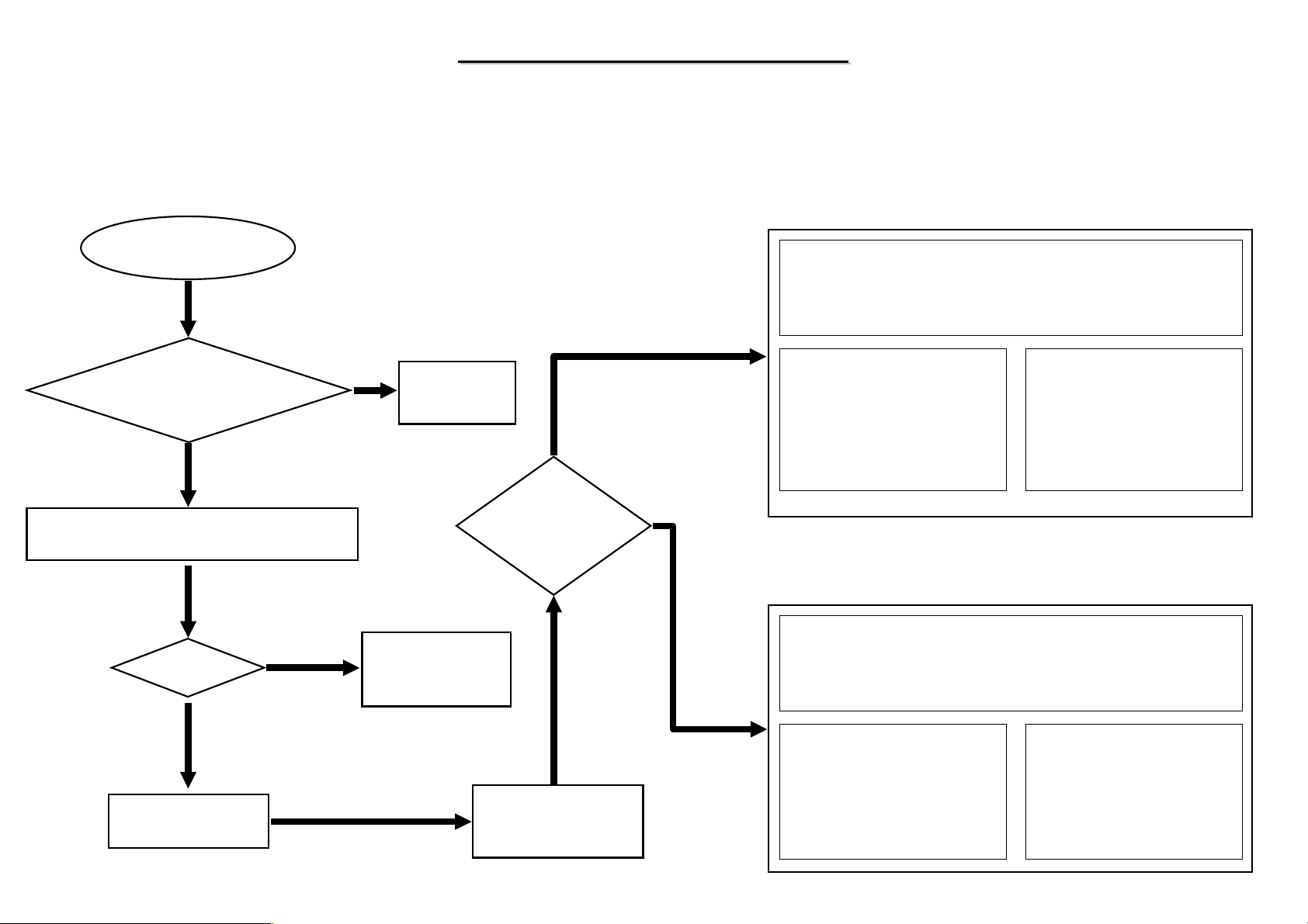
8.1 No Power (2)
When power button is pressed ,nothing happens ,power indicator does not light up.
8599
8599
N/B Maintenance
N/B Maintenance
No Power
Is the
Notebook connected
to power (Either AC adaptor
or battery)?
Yes
Try another known good battery
or AC adapter.
Power
OK?
Yes
No
Replace the faulty
AC adaptor or
Battery.
Connect
AC adaptor
or battery
Where
From Power Source
Problem(First use
AC to power it)
Battery
AC Adaptor
Check the following parts for cold solder or one of the following
parts on the Mother Board may be defective, use an oscilloscope
to check the following signal or replace the parts one at a time and
test after each replacement.
Parts Signal
PJ2
PU22
PD7
PD16
PL21
Check the following parts for cold solder or one of the following
parts on the Mother Board may be defective, use an oscilloscope
to check the following signal or replace the parts one at a time and
test after each replacement.
PL22
PU23
PL19
PR136
PR139
PR146
PQ43
PQ42
PU21
PQ38
PQ39
PQ35
PR125
BATT
BATT_T
BAT_V
DVMAIN
ADINP
ADINP_1
ADINP_2
ADEN#
No
Replace
Motherboard
Board-level
Troubleshooting
PJ1
PF1
PL1
PL2
PL6
Parts Signal
PD4
PQ7
PQ8
PR47
PR48
PD1
PD3
JL503
JL1
PR2
PQ2
PR14
PD2
PU3
PQ12
DVMAIN
SW_+5V
LEARNING
ALWAYS
PWR_ON
+5VA
97
Page 99
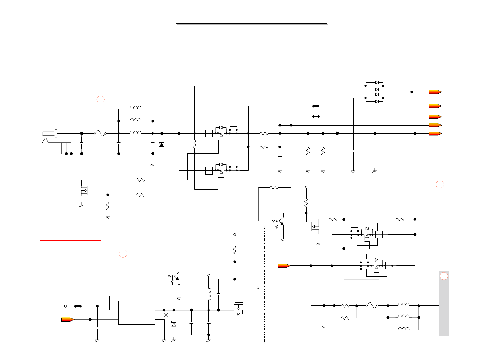
8.1 No Power (3)
When power button is pressed ,nothing happens ,power indicator does not light up.
P23
PF1
PJ1
1
234
PQ2
2N7002
TR/SFT-10A
PC2
0.1U
PR3
100K
PC4
0.1U
PL1
120Z/100M
PL2
120Z/100M
PL6
120Z/100M
PR14
470K
PR2
47K
PC10
0.1U
PQ4
RLZ24D
LEARNING#
8599
8599
PR19
470K
N/B Maintenance
N/B Maintenance
JL503
JL1
G
G
8
7
6
5
D
PQ7
AQ4407
8
7
6
5
D
PQ8
AQ4407
3
2
1
S
3
2
1
S
PR48
0.06
PR47
0.06
PC28
0.1U
PR109
169K
PQ35
DTC144WK
DCP3
PR54
PR107
100K
10K
+3VA
PR55
10K
SM840B
PR112
100K
PD5
PC22
0.1U
DVMAIN
PC24
1000P
BAV70LT1
BAV70LT1
LEARNING#
ADEN#
PD1
PD3
PR111
1M
P20
8
14
W83L950D
ALWAYS
ADINP_1
ADINP_2
ADINP
DVMAIN
U17
KBC
ALWAYS+5VA
ALWAYS
SW_+5VA
PQ36
2N7002
P24
PR45
470K
+5VA
BATT
PQ12
SI2301DS
+5VA
+5V
PL7
PD2
120Z/100M
PC14
0.1U
JS2
PC8
0.1U
8
IN
2
SENSE
7
F/B
3
SHUTDN
PU3
LP2951-02BM
5VTAP
OUT
ERRGND
6
1
5
4
PC21
10U
PC27
0.1U
G
PQ13
SI2301DS
DS
PC132
0.1U
PR126
0.02
PR122
0.02
8
7
6
5
D
4
G
8
7
6
5
TR/SFT-10A
D
PF2
3
2
1
S
PQ39
AQ4407
3
2
1
S
4
G
PQ38
AQ4407
PL16
120Z/100M
PL17
120Z/100M
PL18
120Z/100M
PJ2
P24
2
Battery Connector
98
Page 100
8599
8599
N/B Maintenance
N/B Maintenance
8.2 Battery Can not Be Charged (1)
When the battery is installed but the battery status indicate LED display abnormal.
Battery can not Charge
Is the
notebook connected
to power (AC adaptor)?
Yes
No
Connect
AC adaptor.
Replace
Motherboard
Board-level
Troubleshooting
Check the following parts for cold solder or one of the following
parts on the mother-board may be defective, use an oscilloscope
to check the following signal or replace the parts one at a time and
test after each replacement.2
1. Make sure that the battery is good.
2. Make sure that the battery is installed properly.
Battery charge
OK?
No
Yes
Correct it.
Parts Signal
U17
PU22
PD7
PL21
PL20
PU23
PD16
PL19
PR136
PQ43
PQ42
PR146
PR139
PR140
RP36
D15
RP125
PU21
RP129
RP130
PQ40
ADINP
ADINP_1
ADINP_2
LI_OVP
I_LIMIT
CHG_I
DBATT
BAT_T
BAT_C
BAT_D
BATT_DEAD
99
 Loading...