

Page 1
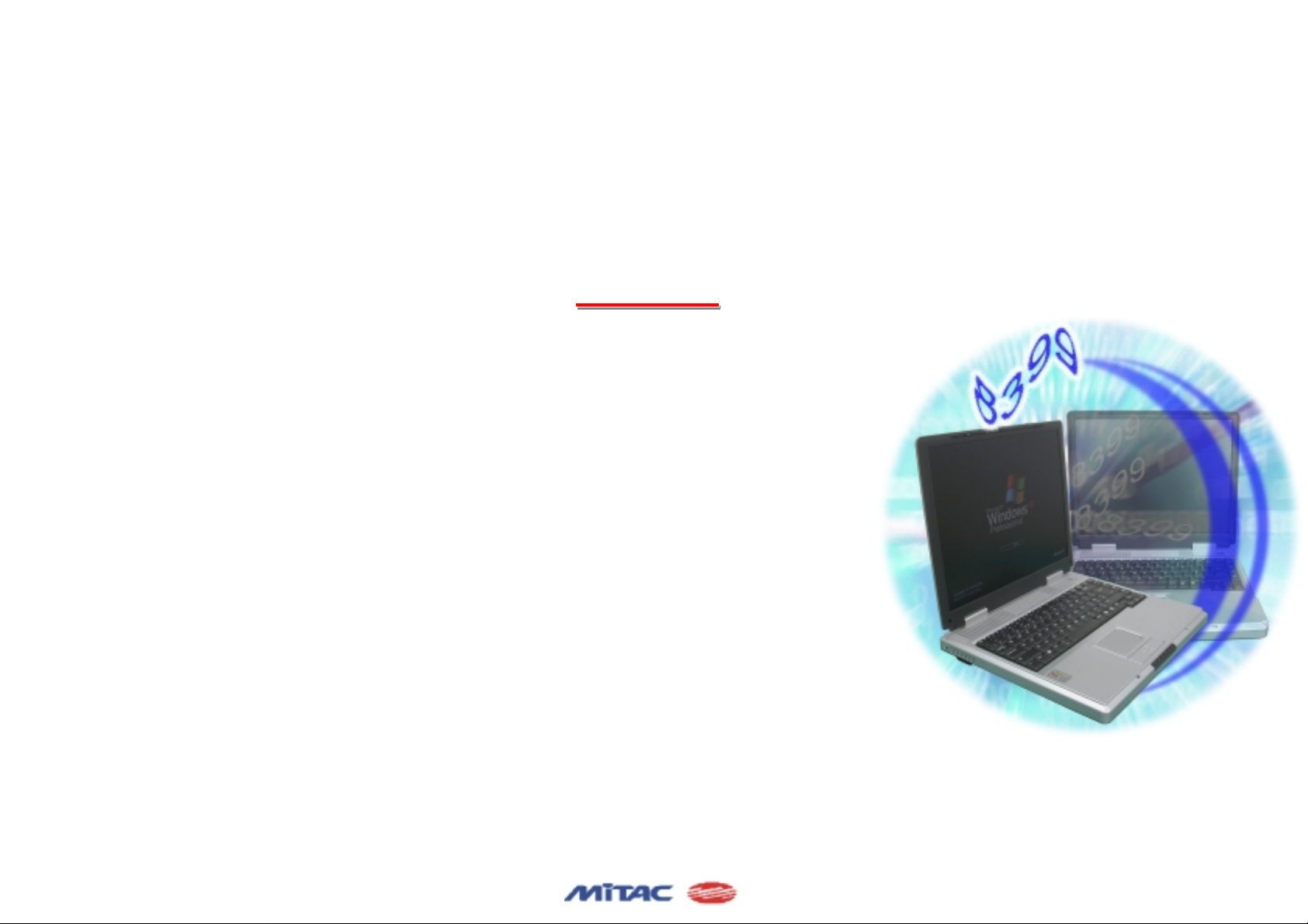
SERVICE MANUAL FOR
SERVICE MANUAL FOR
SERVICE MANUAL FOR
8399
8399
83998399
8399
8399
83998399
8399
8399
83998399
BY:
Repair Technology Research Department /EDVD
Repair Technology Research Department /EDVD
Grass
Grass
Aug.2004
Ren
Ren
Page 2
Contents
8399
8399
N/B Maintenance
N/B Maintenance
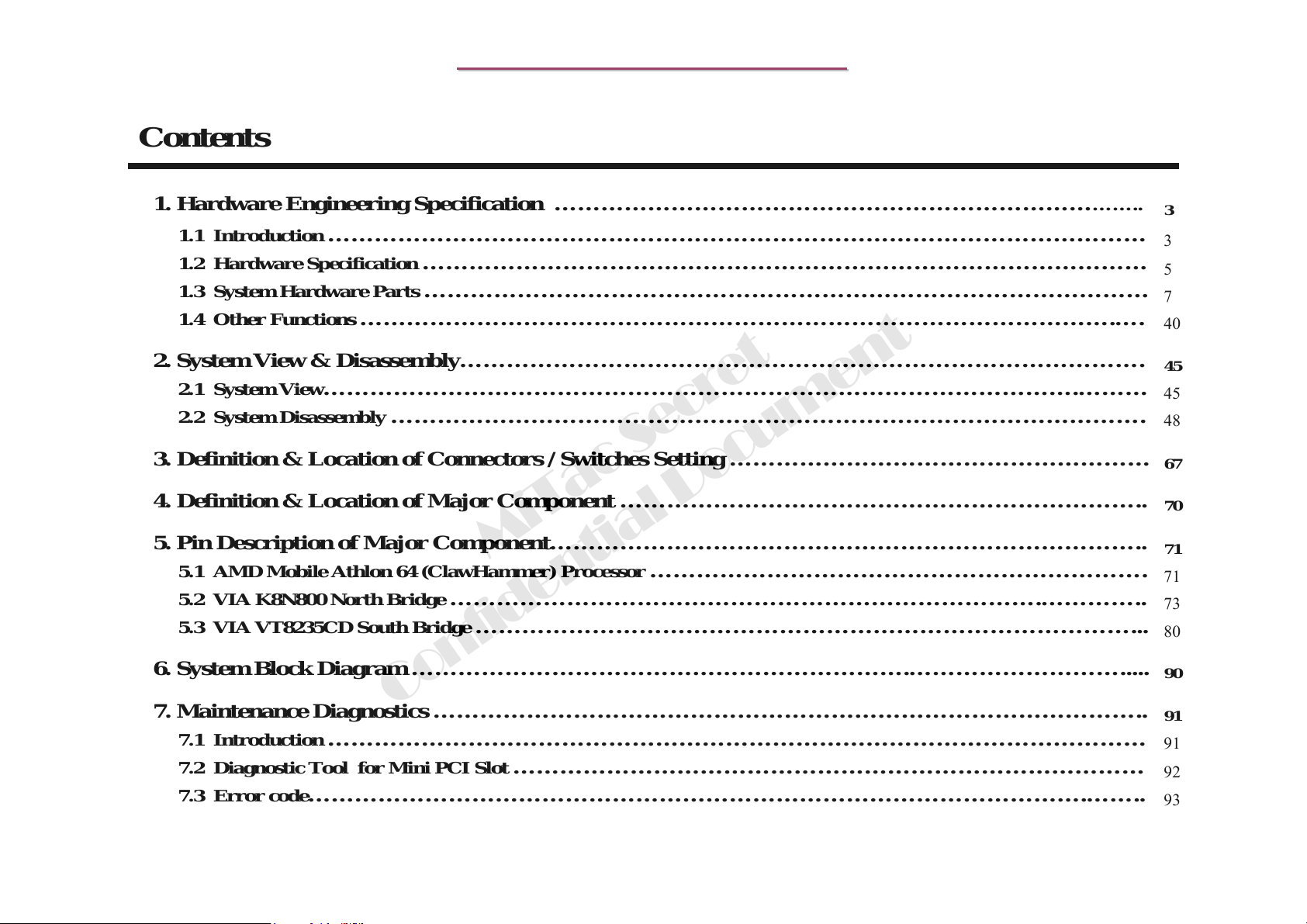
1. Hardware Engineering Specification …………………………………………………………………..
1.1 Introduction
1.2 Hardware Specification …………………………………………………………………………………
1.3 System Hardware Parts …………………………………………………………………………………
1.4 Other Functions …………………………………………………………………………………….….
……………………………………………………………………………………………
2. System View & Disassembly…………………………………………………………………………….
2.1 System View…………………………………………………………………………………….………
2.2 System Disassembly …………………………………………………………………………………….
3. Definition & Location of Connectors / Switches Setting ………………………………………………
4. Definition & Location of Major Component …………………………………………………………..
5. Pin Description of Major Component…………………………………………………………………..
5.1 AMD Mobile Athlon 64 (ClawHammer) Processor ……………………………………………………….
5.2 VIA K8N800 North Bridge ………………………………………………………………….…………..
5.3 VIA VT8235CD South Bridge …………………………………………………………………………...
MiTac Secret
3
3
5
7
40
45
45
48
67
70
71
71
73
80
6. System Block Diagram ……………………………………………………….……………………….....
7. Maintenance Diagnostics ………………………………………………………………………………..
7.1 Introduction ……………………………………………………………………………………………
7.2 Diagnostic Tool for Mini PCI Slot ………………………………………………………………………
7.3 Error code……………………………………………………………………………………….……..
Confidential Document
90
91
91
92
93
1
Page 3
Contents
8399
8399
N/B Maintenance
N/B Maintenance
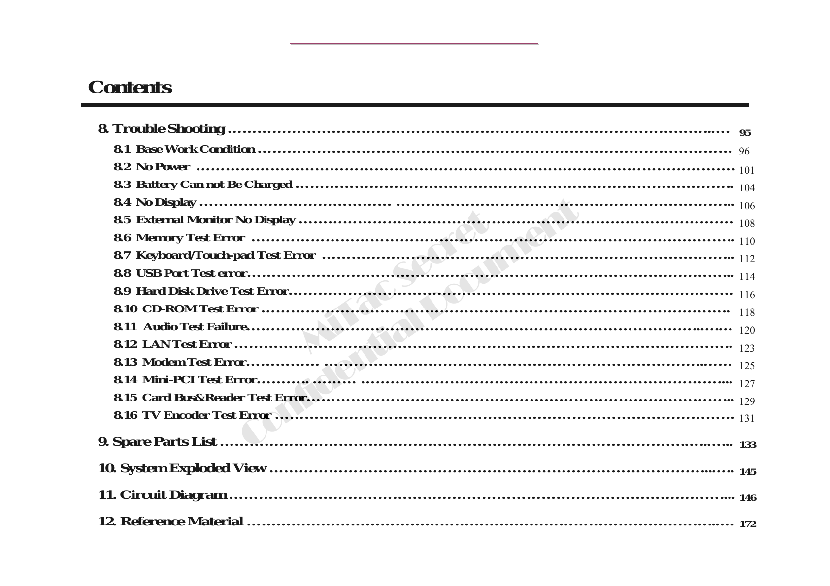
8. Trouble Shooting ……………………………………………………………………………………..….
8.1 Base Work Condition ……………………………………………………………………………………
8.2 No Power ……………………………………………………………………………………………….
8.3 Battery Can not Be Charged ……………………………………………………………………………..
8.4 No Display ………………………………… …………………………………………………………...
8.5 External Monitor No Display …………………………………………………………………………….
8.6 Memory Test Error ……………………………………………………………………………………..
8.7 Keyboard/Touch-pad Test Error ………………………………………………………………………...
8.8 USB Port Test error……………………………………………………………………………………...
8.9 Hard Disk Drive Test Error………………………………………………………………………………
8.10 CD-ROM Test Error …………………………………………………………………………………..
8.11 Audio Test Failure………………………………………………………………………………..….…
8.12 LAN Test Error ………………………………………………………………………………………..
8.13 Modem Test Error…………… …………………………………………………………………..……
8.14 Mini-PCI Test Error……….. ……… ………………………………………………………………....
8.15 Card Bus&Reader Test Error…………………………………………………………………………...
8.16 TV Encoder Test Error …………………………………………………………………………………
MiTac Secret
95
96
101
104
106
108
110
112
114
116
118
120
123
125
127
129
131
9. Spare Parts List ……………………………………………………………………………… ….…..…...
Confidential Document
10. System Exploded View ……………………………………………………………………………...…..
11. Circuit Diagram ………………………………………………………………………………………....
12. Reference Material …………………………………………………………………………………..….
133
145
146
172
2
Page 4

8399
8399
N/B Maintenance
N/B Maintenance
1. Engineer Hardware Specification
1.1 Introduction
The 8399 motherboard would support the AMD K8 62W Dublin (32 bit) with 256KB L2 cache/ Hammer (64 bit)
with 1MB L2 cache with uPGA Package. This system is based on PCI architecture, which have standard hardware
peripheral interface. The power management complies with Advanced Configuration and Power Interface (ACPI)
1.0b. It also provides easy configuration through CMOS setup, which is built in system BIOS software and can be
pop-up by pressing F2 at system start up or warm reset. System also provides icon LEDs to display system status,
such as AC/Battery Power, Battery, WIRELESS LAN status, CD-ROM, HDD, NUM LOCK, CAP LOCK, and
SCROLL LOCK status. It also equipped 6 USB2.0 ports.
The memory subsystem supports 0MB on board; Expandable up to 1024MB Expandable with combination of
optional 128/256/512 MB memory 200-pin DDR 266/333/400 DRAM Memory Module x2, PC-2100/2700/3200
specification.
The “K8N800”chipset is a high performance, cost-effective and energy efficient solution for the implementation of
desktop personal computer systems with 8 / 16-bit 800 / 600 / 400 / 200MHz HyperTransport. CPU host interface
based on AMD K8 / ClawHammer. Processors. The K8N800 north bridge supports a high speed 8-bit 8x66 Mhz
Quad Data Transfer interconnect (V-Link) to the VT8235 South Bridge. These chips also contain a built-in bus-to-
bus bridge to allow simultaneous concurrent operations on each bus. Five levels (double words) of post write buffers
are included to allow for concurrent CPU and V-Link operation. For V-Link Host operation, forty-eight levels
(double words) of post write buffers and sixteen levels (double words) of prefetch buffers are included for
concurrent V-Link bus and DRAM / cache accesses. When combined, the V-Link host / Client controllers realize a
Confidential Document
MiTac Secret
3
Page 5

8399
8399
Complete PCI sub-system and support enhanced PCI bus commands such as “ Master-Read-Line”, “memory-Read-
Multiple” and “Memory-Write-Invalid” commands to minimize snoop overhead. In addition, advanced features are
supported such as snoop ahead, snoop filtering, L1 write-back forward to PCI master, and L1 write-back merged
with PCI post write buffers to minimize PCI master read latency and DRAM utilization. Delay transaction and read
caching mechanisms are also implemented for further improvement of overall system performance.
The VT8235CD “V-Link Client Controller” is a highly integrated PCI /LPC controller. Its internal bus structure is
based on a 66 MHz PCI bus that provides 2x bandwidth compared to previous generation PCI bridge chips. The
VT8235CD also provides a 533 MB/sec bandwidth Host / Client V-Link interface with V-Link-PCI and V-Link-
LPC controllers. It supports six PCI slots of arbitration and decoding for all integrated functions and LPC bus.
To provide for the increasing number of multimedia applications, the AC97 CODEC VT1617/1617A is integrated
onto the motherboard
N/B Maintenance
N/B Maintenance
A full set of software drivers and utilities are available to allow advanced operating systems such as Windows XP
and Windows 2000 to take full advantage of the hardware capabilities such as bus mastering IDE, Plug & Play, and
Advance configuration and power interface(ACPI).
Following chapters will have more detail description for each individual sub-systems and functions.
MiTac Secret
Confidential Document
4
Page 6
8399
8399
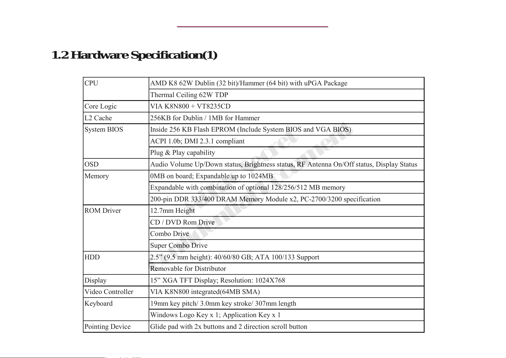
1.2 Hardware Specification(1)
CPU AMD K8 62W Dublin (32 bit)/Hammer (64 bit) with uPGA Package
Thermal Ceiling 62W TDP
Core Logic VIA K8N800 + VT8235CD
L2 Cache 256KB for Dublin / 1MB for Hammer
System BIOS Inside 256 KB Flash EPROM (Include System BIOS and VGA BIOS)
ACPI 1.0b; DMI 2.3.1 compliant
Plug & Play capability
OSD Audio Volume Up/Down status, Brightness status, RF Antenna On/Off status, Display Status
Memory 0MB on board; Expandable up to 1024MB
Expandable with combination of optional 128/256/512 MB memory
N/B Maintenance
N/B Maintenance
200-pin DDR 333/400 DRAM Memory Module x2, PC-2700/3200 specification
ROM Driver 12.7mm Height
CD / DVD Rom Drive
Combo Drive
Super Combo Drive
HDD 2.5” (9.5 mm height): 40/60/80 GB; ATA 100/133 Support
Removable for Distributor
Confidential Document
Display 15” XGA TFT Display; Resolution: 1024X768
Video Controller VIA K8N800 integrated(64MB SMA)
Keyboard 19mm key pitch/ 3.0mm key stroke/ 307mm length
Windows Logo Key x 1; Application Key x 1
Pointing Device Glide pad with 2x buttons and 2 direction scroll button
MiTac Secret
5
Page 7
8399
8399
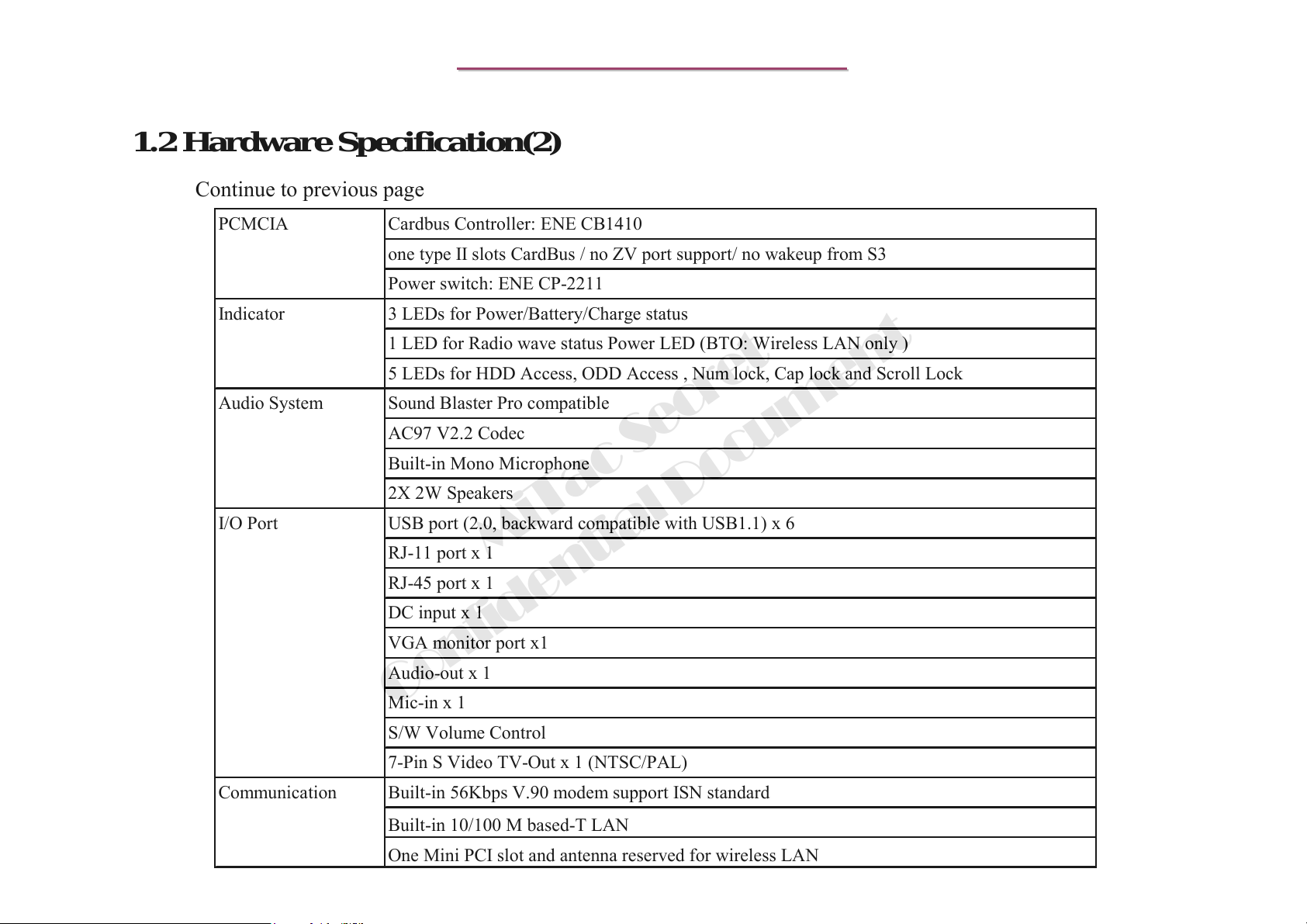
1.2 Hardware Specification(2)
Continue to previous page
PCMCIA Cardbus Controller: ENE CB1410
one type II slots CardBus / no ZV port support/ no wakeup from S3
Power switch: ENE CP-2211
Indicator 3 LEDs for Power/Battery/Charge status
1 LED for Radio wave status Power LED (BTO: Wireless LAN only )
5 LEDs for HDD Access, ODD Access , Num lock, Cap lock and Scroll Lock
Audio System Sound Blaster Pro compatible
AC97 V2.2 Codec
Built-in Mono Microphone
2X 2W Speakers
N/B Maintenance
N/B Maintenance
I/O Port USB port (2.0, backward compatible with USB1.1) x 6
RJ-11 port x 1
RJ-45 port x 1
DC input x 1
VGA monitor port x1
Audio-out x 1
Confidential Document
Mic-in x 1
S/W Volume Control
7-Pin S Video TV-Out x 1 (NTSC/PAL)
Communication Built-in 56Kbps V.90 modem support ISN standard
Built-in 10/100 M based-T LAN
One Mini PCI slot and antenna reserved for wireless LAN
MiTac Secret
6
Page 8
8399
8399
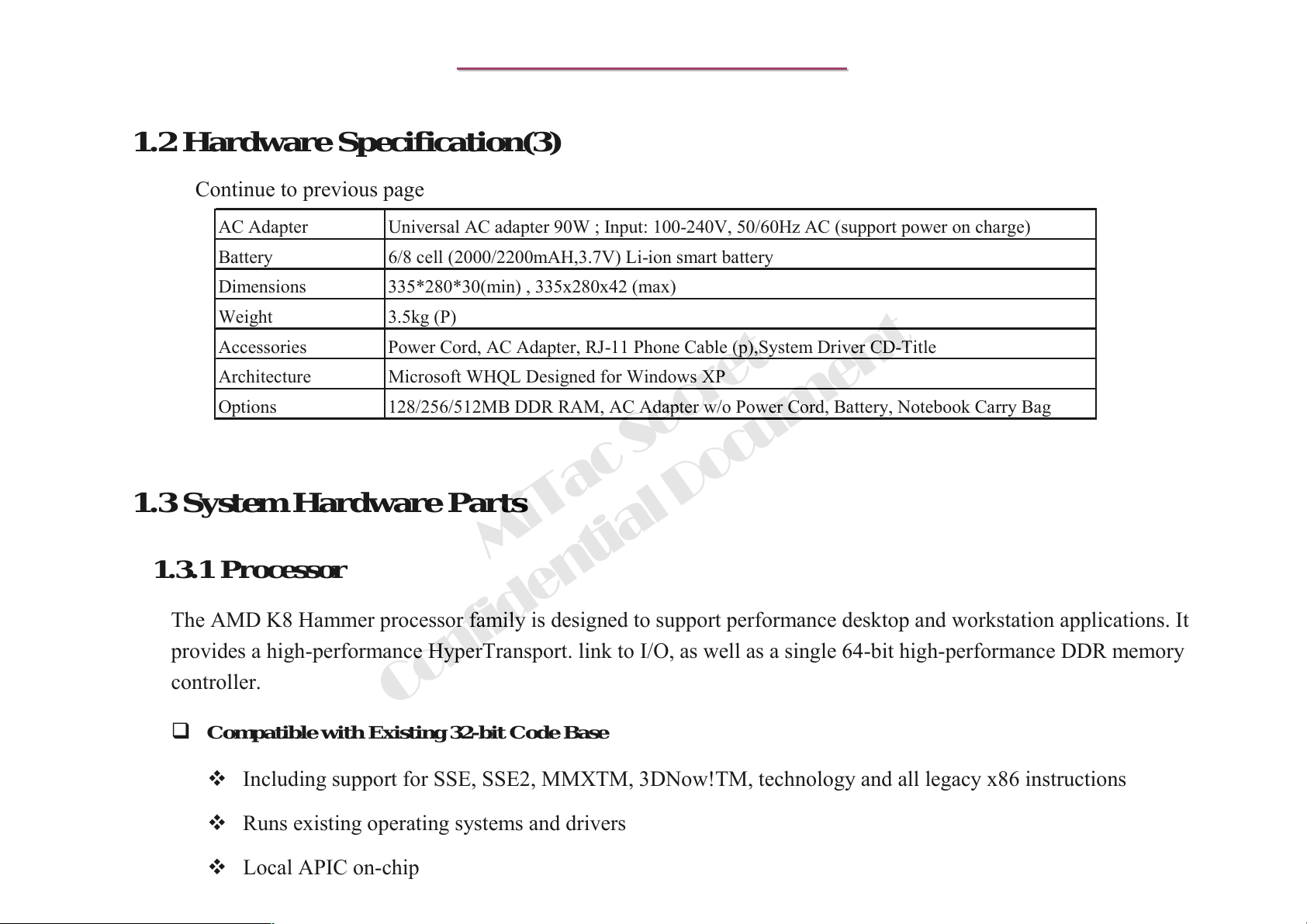
1.2 Hardware Specification(3)
Continue to previous page
AC Adapter Universal AC adapter 90W ; Input: 100-240V, 50/60Hz AC (support power on charge)
Battery 6/8 cell (2000/2200mAH,3.7V) Li-ion smart battery
Dimensions 335*280*30(min) , 335x280x42 (max)
Weight 3.5kg (P)
Accessories Power Cord, AC Adapter, RJ-11 Phone Cable (p),System Driver CD-Title
Architecture Microsoft WHQL Designed for Windows XP
Options 128/256/512MB DDR RAM, AC Adapter w/o Power Cord, Battery, Notebook Carry Bag
N/B Maintenance
N/B Maintenance
1.3 System Hardware Parts
MiTac Secret
1.3.1 Processor
The AMD K8 Hammer processor family is designed to support performance desktop and workstation applications. It
provides a high-performance HyperTransport. link to I/O, as well as a single 64-bit high-performance DDR memory
controller.
Confidential Document
Compatible with Existing 32-bit Code Base
Including support for SSE, SSE2, MMXTM, 3DNow!TM, technology and all legacy x86 instructions
Runs existing operating systems and drivers
Local APIC on-chip
7
Page 9
8399
8399
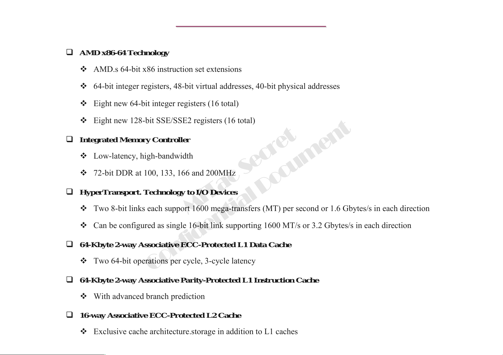
AMD x86-64 Technolo gy
AMD.s 64-bit x86 instruction set extensions
64-bit integer registers, 48-bit virtual addresses, 40-bit physical addresses
Eight new 64-bit integer registers (16 total)
Eight new 128-bit SSE/SSE2 registers (16 total)
Integrated Memory Controller
Low-latency, high-bandwidth
72-bit DDR at 100, 133, 166 and 200MHz
HyperTransport. Technology to I/O Devices
N/B Maintenance
N/B Maintenance
Two 8-bit links each support 1600 mega-transfers (MT) per second or 1.6 Gbytes/s in each direction
Can be configured as single 16-bit link supporting 1600 MT/s or 3.2 Gbytes/s in each direction
64-Kbyte 2-way Associative ECC-Protected L1 Data Cache
Two 64-bit operations per cycle, 3-cycle latency
MiTac Secret
Confidential Document
64-Kbyte 2-way Associative Parity-Protected L1 Instruction Cache
With advanced branch prediction
16-way Associative ECC-Protected L2 Cache
Exclusive cache architecture.storage in addition to L1 caches
8
Page 10
8399
8399
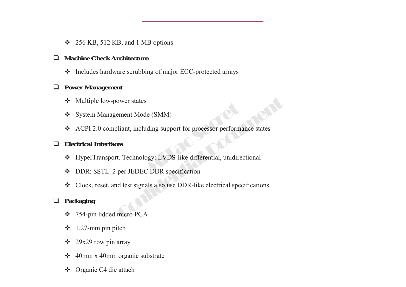
256 KB, 512 KB, and 1 MB options
Machine Check Architecture
Includes hardware scrubbing of major ECC-protected arrays
Power Management
Multiple low-power states
System Management Mode (SMM)
ACPI 2.0 compliant, including support for processor performance states
Electrical Interfaces
N/B Maintenance
N/B Maintenance
HyperTransport. Technology: LVDS-like differential, unidirectional
DDR: SSTL_2 per JEDEC DDR specification
Clock, reset, and test signals also use DDR-like electrical specifications
Packaging
754-pin lidded micro PGA
1.27-mm pin pitch
29x29 row pin array
40mm x 40mm organic substrate
Organic C4 die attach
Confidential Document
MiTac Secret
9
Page 11

8399
8399
N/B Maintenance
N/B Maintenance
1.3.2 K8N800 North Bridge
The “K8N800”chipset is a high performance, cost-effective and energy efficient solution for the implementation of
mobile personal computer systems with 8 / 16-bit 800 / 600 / 400 / 200 MHz HyperTransport. CPU host interface
based on AMD K8 / Claw Hammer processors.
Defines Highly Integrated Solutions for Performance PC Desktop Designs
High performance North Bridge with HyperTransport. interface to AMD K8 CPU plus AGP 8x external bus
to external Graphics Controller plus high-speed V-Link interface to South Bridge.
Combines with VIA VT8235CD V-Link South Bridge for integrated LAN, Audio, ATA133 IDE, and 6
USB 2.0 ports
587 Ball Grid Array package with 35 x 35 mm body size, 1.27mm ball pitch
1.5V core, 0.15 u process
High Performance HyperTransport CPU Interface
Chipset support for AMD. K8 / ClawHammer. Processor
Processor interface via HyperTransport. Bus
Separate “transmit” and “receive” buses for no lost “bus turnaround” cycles
All transmit and receive signals use 2 pin low-voltage-swing differential signalling for high-reliability and
high speed
8 or 16-bit control / address / data transfer both directions
Confidential Document
MiTac Secret
10
Page 12
8399
8399
800 / 600 / 400 / 200 MHz clock rates with “Double Data Rate”-style operation for 1600/1200/800/400
MT/s in both directions simultaneously (total 6.4GB/sec using 16-bit transfer mode)
Default 8-bit / 200 MHz operation on startup for high reliability with speedup to dual 16-bit, 800 MHz
operation (6.4 GB/sec total bandwidth) under software control (transmit and receive may be different widths
and / or speeds)
Full Featured Accelerated Graphics Port (AGP) 8x Controller
Supports 533 MHz 8x, 266 MHz 4x, and 133 MHz 2x transfer modes for AD and SBA signaling
AGP v3.0 compliant with 8x transfer mode
Pseudo-synchronous with the host CPU bus with optimal skew control
Supports SideBand Addressing (SBA) mode (non-multiplexed address / data)
N/B Maintenance
N/B Maintenance
AGP pipelined split-transaction long-burst transfers up to 1GB/sec
Eight level read request queue
Four level posted-write request queue
Thirty-two level (quadwords) read data FIFO (256 bytes)
MiTac Secret
Confidential Document
Sixteen level (quadwords) write data FIFO (128 bytes)
Intelligent request reordering for maximum AGP bus utilization
Supports Flush/Fence commands
Graphics Address Relocation Table (GART)
11
Page 13
8399
8399
One level TLB structure
Sixteen entry fully associative page table
LRU replacement scheme
Independent GART lookup control for host / AGP / PCI master accesses
Windows 95 OSR-2 VXD and integrated Windows 98 / 2000 / XP mini port driver support
High Bandwidth 533 MB / Sec 8-bit V-Link Host Controller South Bridge Interface
Supports 66 MHz V-Link Host interface with total bandwidth of 533 MB/sec
Operates in 2x, 4x, and 8x modes
Full duplex commands with separate command / strobe for 4x / 2x mode, half-duplex for 8x mode
N/B Maintenance
N/B Maintenance
Request / Data split transaction
Configurable outstanding transaction queue for Host to V-Link Client accesses
Supports Defer / Defer-Reply transactions
Transaction assurance for V-Link Host to Client access eliminates V-Link Host-Client Retry cycles
MiTac Secret
Confidential Document
Intelligent V-Link transaction protocol to eliminate data wait-state / throttle transfer Latency
All V-Link transactions for both Host and Client have a consistent view of transaction data depth and buffer
size to avoid data overflow
Highly efficient V-Link arbitration with minimum overhead
12
Page 14
8399
8399
All V-Link transactions have predictable cycle length with known command / data duration
Integrated Graphics / Video Accelerator
Optimized Share Memory Architecture (SMA)
16 / 32 / 64 MB frame buffers using system memory
Internal AGP 8x equivalent performance
Separate 128-bit data paths between north bridge and graphics core for pixel data flow and texture/command
access
Graphics engine clock up to 200MHz decoupled form memory clock
High quality DVD video playback
N/B Maintenance
N/B Maintenance
Internal hardware VGA controller with true-color / high-color sprite for hardware cursor implementation
MiTac Secret
128-bit 2D graphics engine
128-bit 3D graphics engine
Floating point triangle setup engine
Microsoft DirectX texture compression
4.5M triangles/second setup engine
400M texels/second bilinear fill rate
Confidential Document
13
Page 15
8399
8399
Extensive Display Support
CRT display interface with 24-bit true-color RAMDAC up to 300MHz pixel rate with gamma correction
capability
DFP” flat panel interface supporting single-channel or dual-channel LVDS encoders
DVI” Flat Panel Monitor 12-bit DVI 1.0-compatible interface designed for use with external TMDS encoder
AGP 8x / 4x functions muxed on DFP/DVI pins for optional external graphics controller upgrade module
Dedicated 12-bit interface to TV Encoder for NTSC or PAL TV display (may be optionally configured as
12-bit DVI 1.0 interface to external TMDS encoder for driving a Flat Panel Monitor)
DuoView+ Dual Image Capability
N/B Maintenance
N/B Maintenance
Direct Win98, WinME and WinXP multi-monitor, extended desktop support
MiTac Secret
Independent resolution and color depth for secondary desktop
Improved display flexibility with simultaneous LCD/CRT, CRT/DVI, CRT/TV, LCD/TV, DVI/TV
operation capability
CRT, LCD or TV refresh rates are independently programmable to allow optimum image quality
Enables different images on different displays simultaneously for true multitasking
Full Media capabilities on all displays
Support for CRT resolutions up to 1920x1440 and panel resolutions up to 1600x1200
Automatic panel power sequencing and VESA DPMS CRT power-down
Confidential Document
14
Page 16
8399
8399
Built-in reference voltage generator and monitor sense circuits
I2C Serial Bus and DDC Monitor Communications for CRT Plug-and-Play configuration
Video Support
High quality 5-tap horizontal and 5-tap vertical scaler (up or down) for both horizontal and vertical scaling
(linear interpolation for horizontal and vertical p-scaling filtering for horizontal and vertical down-scaling)
Color space conversion
Color enhancement (contrast, hue, saturation, brightness, and gamma correction)
Color and chroma key support
Hardware sub-picture blending
N/B Maintenance
N/B Maintenance
Bob / weave de-interlacing mode and advanced de-interlacing to improve video quality
MiTac Secret
Video gamma correction
PAL / NTSC TV output capability using external TV encoder
Support CCIR601 standard
MPEG-2/1 Video Decoder
MPEG-2 hardware slice layer, iDCT, and motion compensation for full speed DVD playback
2-D Hardware Acceleration Features
BitBLT 9bit block transfer) functions including alpha blts
Confidential Document
15
Page 17
8399
8399
Text function
Bresenham line drawing / style line function
ROP3, 256 operation
Color expansion
Source and destination color keys
Transparency mode
Window clipping
8, 16, and 32 bpp mode acceleration
3-D Hardware Acceleration Features
N/B Maintenance
N/B Maintenance
Microsoft DirectX 7.0 and 8.0 compatible
MiTac Secret
OpenGL driver available
Floating-point setup engine
Triangle rate up to 4.5-million triangles per second and Pixel rate up to 400 million pixels per second for 2
texture, depth test and alpha blending
8K Texture Cache
Microsoft DirectX Texture Compression (S3TC)
Flat and Gouraud shading
Hardware back-face culling
Confidential Document
16
Page 18
8399
8399
16-bit, 32-bit Z test, and 24+8 Z+ Stencil test support
Z-Bias support
Stipple Test, Line-Pattern test, Text re-Transparence test, Alpha test support
Edge anti-aliasing support
Two textures per pass
Tremendous Texture Format: 16/32 bpp ARGB, 1/2/4/8 bpp Luminance, 1/2/4/8 bpp Intensity, 1/2/4/8 bpp
Paletized (ARGB) , YUV 422/420 format
Texture sizes up to 2048x2048
High quality texture filter modes: Nearest, Linear, Bi-linear, Tri-linear, Anisotropic
N/B Maintenance
N/B Maintenance
LOD-Bias support
MiTac Secret
Vertex Fog and Fog Talbe
Specular Lighting
Alpha Blending
Bump mapping
High quality dithering
ROP2 support
Internal full 32-bit ARGB format for high rendering quality
Confidential Document
17
Page 19
8399
8399
System balance to achieve high performance
Advanced System Power Management
Power down of SDRAM (CKE)
Independent clock stop controls for CPU, DDR SDRAM, VLINK interface, graphics engine (2D,3D, video,
display) and on-chip AGP bus
Suspend power plane for preservation of memory data
Suspend-to-DRAM and self-refresh power down
Low-leakage I/O pads
ACPI 1.0B and PCI Bus Power Management 1.1 compliant
N/B Maintenance
N/B Maintenance
Full Software Support
MiTac Secret
Drivers for major operating system and APIs (windows 9x, Windows NT, Windows2000,Windows XP,
Direct3D, DirectDraw and DirectShow, OpenGL ICD for Windows 9x, NT, 2000, and XP)
Chipset and Video BIOS support (including all standard VESZA CRT display modes)
Confidential Document
1.3.3 VIA VT8235CD BGA PCI-LPC/ISA South Bridge
The VT8235CD South Bridge is a high integration, high performance, power-efficient, and high compatibility
device that supports Intel and non-Intel based processor to V-Link bus bridge functionality to make a complete
Microsoft PC2001-compliant PCI/LPC system. The VT8235CD includes standard intelligent peripheral controllers:
18
Page 20
8399
8399
IEEE 802.3 compliant 10 / 100 Mbps PCI bus master Ethernet MAC with standard MII interface to external
PHYceiver.
Master mode enhanced IDE controller with dual channel DMA engine and interlaced dual channel
commands. Dedicated FIFO coupled with scatter and gather master mode operation allows high
performance transfers between PCI and IDE devices. In addition to standard PIO and DMA mode operation,
the VT8235CD also supports the UltraDMA-133, 100, 66, and 33 standards to allow reliable data transfer at
rates up to 133 MB/sec. The IDE controller is SFF-8038i v1.0 and Microsoft Windows-family compliant.
Universal Serial Bus controller that is USB v2.0 / 1.1 and Universal HCI v2.0 / 1.1 compliant. The
VT8235CD includes three root hubs with six function ports with integrated physical layer transceivers. The
USB controller allows hot plug and play and isochronous peripherals to be inserted into the system with
universal driver support. The controller also implements legacy keyboard and mouse support so that legacy
N/B Maintenance
N/B Maintenance
software can run transparently in a non-USB-aware operating system environment.
Keyboard controller with PS2 mouse support.
Real Time Clock with 256 byte extended CMOS. In addition to the standard ISA RTC functionality, the
integrated RTC also includes the date alarm, century field, and other enhancements for compatibility with
the ACPI standard.
Notebook-class power management functionality compliant with ACPI and legacy APM requirements.
Multiple sleep states (power-on suspend, suspend-to-DRAM, and suspend-to-Disk) are supported with
hardware automatic wake-up. Additional functionality includes event monitoring, CPU clock throttling and
stop (Intel processor protocol), PCI bus clock stop control, modular power, clock and leakage control,
hardware-based and software-based event handling, general purpose I/O, chip select and external SMI.
Full System Management Bus (SMBus) interface.
Confidential Document
MiTac Secret
19
Page 21
8399
8399
N/B Maintenance
N/B Maintenance
Integrated bus-mastering dual full-duplex direct-sound AC97-link-compatible sound system.
Plug and Play controller that allows complete steer ability of all PCI interrupts and internal interrupts / DMA
channels to any interrupt channel. One additional steerable interrupt channel is provided to allow plug and
play and reconfigure ability of onboard peripherals for Windows family compliance.
The VT8235CD also enhances the functionality of the standard ISA peripherals. The integrated interrupt controller
supports both edge and level triggered interrupts channel by channel. The integrated DMA controller supports type F
DMA in addition to standard ISADMA modes. Compliant with the PCI-2.2 specification, the VT8235CD supports
delayed transactions and remote power management so that slower ISA peripherals do not block the traffic of the
PCI bus. Special circuitry is built in to allow concurrent operation without causing dead lock even in a PCI-to-PCI
bridge environment. The chip also includes eight levels (double words) of line buffers from the PCI bus to the ISA
bus to further enhance overall system performance.
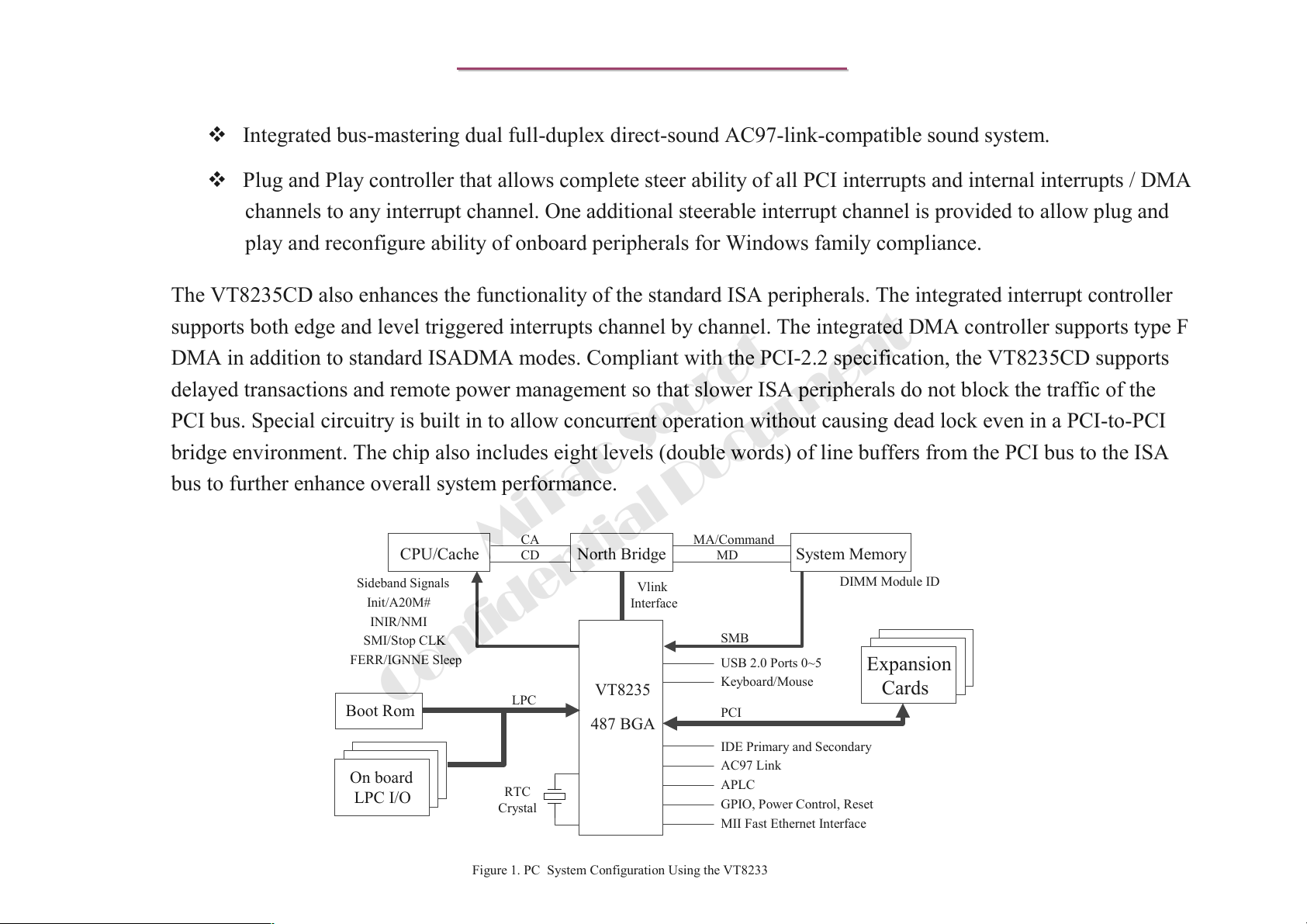
CPU/Cache North Bridge System Memory
Sideband Signals
Init/A20M#
INIR/NMI
SMI/Stop CLK
FERR/IGNNE Sleep
Boot Rom
Confidential Document
On board
LPC I/O
CA
MiTac Secret
CD
Vlink
Interface
LPC
RTC
Crystal
Figure 1. PC System Configuration Using the VT8233
VT8235
487 BGA
MA/Command
MD
SMB
USB 2.0 Ports 0~5
Keyboard/Mouse
PCI
IDE Primary and Secondary
AC97 Link
APLC
GPIO, Power Control, Reset
MII Fast Ethernet Interface
DIMM Module ID
Expansion
Cards
20
Page 22
8399
8399
Inter-operable with VIA Host-to-V-Link Host Controller
Combine with VT8754 (Apollo P4X333) for a complete 533 / 400 MHz FSB Pentium 4 system
Combine with VT8377 (Apollo KX400) for a complete 266 / 200 MHz FSB Athlon Socket-A system
May be used interchangeably with the VT8235CDLSout h Bridge in most board designs
High Bandwidth 533 MB/s 8-bit V-Link Client Controller
Supports 66 MHz V-Link Client interface with peak bandwidth of 533 MB/sec
V-Link operates in 2x, 4x, and 8x modes
Full duplex commands with separate Strobe / Command
N/B Maintenance
N/B Maintenance
Request / Data split transaction
Configurable outstanding transaction queue for V-Link Client accesses
Auto Client Retry to eliminate V-Link Host-Client Retry cycles
Intelligent V-Link transaction protocol to eliminate data wait-state / throttle transfer latency; all V-Link
transactions for both Host and Client have a consistent view of transaction data depth and buffer size to
avoid data overflow.
Highly efficient V-Link arbitration with minimum overhead; all V-Link transactions have predictable cycle
length with known Command / Data duration
Auto connect / reconnect capability and dynamic stop for minimum power consumption
Parity checking to insure correct data transfers
Confidential Document
MiTac Secret
21
Page 23
8399
8399
Integrated Peripheral Controllers
Integrated Fast Ethernet Controller with 1 / 10 / 100 Mbit capability
Integrated USB 2.0 Controller with three root hubs and six function ports
Dual channel UltraDMA-133 / 100 / 66 / 33 master mode EIDE controller
AC-link interface for AC-97 audio codec and modem codec
HSP modem support
Integrated DirectSound compatible digital audio controller
LPC interface for Low Pin Count interface to Super-I/O or ROM
Integrated Legacy Functions
N/B Maintenance
N/B Maintenance
Integrated Keyboard Controller with PS2 mouse support
Integrated DS12885-style Real Time Clock with extended 256 byte CMOS RAM and Day/Month Alarm for
ACPI
Integrated DMA, timer, and interrupt controller
Serial IRQ for docking and non-docking applications
Fast reset and Gate A20 operation
Concurrent PCI Bus Controller
33 MHz operation
Confidential Document
MiTac Secret
22
Page 24
8399
8399
Supports up to six PCI masters
Peer concurrency
Concurrent multiple PCI master transactions; i.e., allow PCI masters from both PCI buses active at the same
time
Zero wait state PCI master and slave burst transfer rate
PCI to system memory data streaming up to 132Mbyte/sec (data sent to north bridge via high speed V-Link
Interface)
PCI master snoop ahead and snoop filtering
Eight DW of CPU to PCI posted write buffers
N/B Maintenance
N/B Maintenance
Byte merging in the write buffers to reduce the number of PCI cycles and to create further PCI bursting
possibilities
Enhanced PCI command optimization (MRL, MRM, MWI, etc.)
Four lines of post write buffers from PCI masters to DRAM
Sixteen levels (double-words) of prefetch buffers from DRAM for access by PCI masters
MiTac Secret
Confidential Document
Delay transaction from PCI master accessing DRAM
Transaction timer for fair arbitration between PCI masters (granularity of two PCI clocks)
Symmetric arbitration between Host/PCI bus for optimized system performance
Complete steerable PCI interrupts
23
Page 25
8399
8399
PCI-2.2 compliant, 32 bit 3.3V PCI interface with 5V tolerant inputs
Fast Ethernet Controller
High performance PCI master interface with scatter / gather and bursting capability
Standard MII interface to external PHYceiver
1 / 10 / 100 MHz full and half duplex operation
Independent 2K byte FIFOs for receive and transmit
Flexible dynamically loadable EEPROM algorithm
Physical, Broadcast, and Multicast address filtering using hashing function
Magic packet and wake-on-address filtering
N/B Maintenance
N/B Maintenance
Software controllable power down
UltraDMA- 133/ 100 / 66 / 33 Master Mode EIDE Controller
Dual channel master mode hard disk controller supporting four Enhanced IDE devices
Transfer rate up to 133MB/sec to cover PIO mode 4, multi-word DMA mode 2 drives, and UltraDMA-133
MiTac Secret
Confidential Document
interface
Increased reliability using UltraDMA-133/100/66 transfer protocols Thirty-two levels (double words) of
prefetch and write buffers
Dual DMA engine for concurrent dual channel operation
24
Page 26
8399
8399
Bus master programming interface for SFF-8038i rev.1.0 and Windows-95 compliant
Full scatter gather capability
Support ATAPI compliant devices including DVD devices
Support PCI native and ATA compatibility modes
Complete software driver support
Direct Sound Ready AC97 Digital Audio Controller
AC-Link access to 4 CODECs (AC97 + AMC97 + MC97)
Multi channel Audio
Bus Master Scatter / Gather DMA
N/B Maintenance
N/B Maintenance
Dedicated read and write channels supporting simultaneous stereo playback and record
Dedicated read and write channels supporting simultaneous modem receive and transmit
1 stereo DirectSound channel with source / volume control / mixer
1 shared FM / SPDIF PCM read channel
MiTac Secret
Confidential Document
1 dedicated channel supporting multi-channel audio
32-byte line-buffers for each SGD channel
Programmable 8bit / 16bit mono / stereo PCM data format support
AC97 2.1 compliant
25
Page 27
8399
8399
System Management Bus Interface
Host interface for processor communications
Slave interface for external SMBus masters
Universal Serial Bus Controller
USB v2.0 and Enhanced Host Controller Interface (EHCI) v1.0 compatible
USB v1.1 and Universal Host Controller Interface (UHCI) v1.1 compatible
Eighteen level (double words) data FIFO with full scatter and gather capability
Three root hubs and six function ports
N/B Maintenance
N/B Maintenance
Integrated physical layer transceivers with optional over-current detection status on USB inputs
Legacy keyboard and PS/2 mouse support
Sophisticated PC2001-Compatible Mobile Power Manage ment
Supports both ACPI (Advanced Configuration and Power Interface) and legacy (APM) power management
ACPI v1.0 Compliant
MiTac Secret
Confidential Document
APM v1.2 Compliant
CPU clock throttling and clock stop control for complete ACPI C0 to C3 state support
PCI bus clock run, Power Management Enable (PME) control, and PCI/CPU clock generator stop control
Supports multiple system suspend types: power-on suspends with flexible CPU/PCI bus reset options,
26
Page 28
8399
8399
suspend to DRAM, and suspend to disk (soft-off), all with hardware automatic wake-up
Multiple suspend power plane controls and suspend status indicators
One idle timer, one peripheral timer and one general purpose timer, plus 24/32-bit ACPI compliant timer
Normal, doze, sleep, suspend and conserve modes
Global and local device power control
System event monitoring with two event classes
Primary and secondary interrupt differentiation for individual channels
Dedicated input pins for power and sleep buttons, external modem ring indicator, and notebook lid
open/close for system wake-up
N/B Maintenance
N/B Maintenance
32 general purpose input ports and 32 output ports
MiTac Secret
Multiple internal and external SMI sources for flexible power management models
Enhanced integrated real time clock (RTC) with date alarm, month alarm, and century field
Thermal alarm on external temperature sensing circuit
I/O pad leakage control
Plug and Play Controller
PCI interrupts steerable to any interrupt channel
Steerable interrupts for integrated peripheral controllers: USB, floppy, serial, parallel, and audio
Confidential Document
27
Page 29
8399
8399
Microsoft Windows XPTM, Windows NTTM, Windows 2000TM, Windows 98TM and plug and play BIOS
compliant
Built-in NAND-tree pin scan test capability
0.22um, 2.5V, low po wer CMOS process
Single chip 27 x 27 mm, 1.0 mm ball pitch, 487 pin BGA
N/B Maintenance
N/B Maintenance
1.3.4 System Frequency Synthesizer and DDR-SDRAM Buffer: ICS950403
The ICS950403 is a system clock synthesizer chip for AMD K8 based notebook systems with AMD, VIA or Ali
chipset. This provides all clocks required for such a system. The ICS950403 employs a proprietary closed loop
design, which tightly controls the percentage of spreading over process and temperature variations. Serial
MiTac Secret
programming I 2 C interface allows changing functions, stop clock programming and frequency selection.
Output Features
2 - Differential pair push-pull CPU clocks @ 3.3V
8 - PCICLK (Including 1 free running) @ 3.3 V
3 - Selectable PCICLK/HTTCLK @ 3.3V
1 - HTTCLK @ 3.3V
1 - 48MHz @ 3.3V fixed
Confidential Document
28
Page 30
8399
8399
1 - 24_48MHz @ 3.3V
3 - REF @ 3.3V, 14.318MHz
Features/Benefits
Programmable output frequency
Programmable output divider ratios
Programmable output rise/fall time
Programmable output skew
Programmable spread percentage for EMI control
Watchdog timer technology and RESET# output to reset system if system malfunction
N/B Maintenance
N/B Maintenance
Programmable watch dog safe frequency
MiTac Secret
Support I2C index read/write and block read/write operations
Uses external 14.318MHz crystal
Support Hyper Transport Technology (HTTCLK)
Confidential Document
48-Pin 300mil SSOP
29
Page 31
8399
8399
N/B Maintenance
N/B Maintenance
1.3.5 PC Card Interface Controller: ENE CB1410
The ENE CB1410 is a high-performance PCI-to-PC Card controller that supports a single PC Card socket compliant
with the 1997 PC Card Standard. The ENE CB1410 provides features that make it the best choice for bridging
between PCI and PC Cards in both notebook and desktop computers. The 1997 PC Card Standard retains the 16-bit
PC Card specification defined in PCI Local Bus Specification and defines the new 32-bit PC Card, CardBus, capable
of full 32-bit data transfers at 33 MHz. The ENE CB1410 supports both 16-bit and CardBus PC Cards, powered at 5
V or 3.3 V, as required.
The ENE CB1410 is compliant with the PCI Local Bus Specification, and its PCI interface can act as either a PCI
master device or a PCI slave device. The PCI bus mastering is initiated during 16-bit PC Card DMA transfers or
CardBus PC Card bridging transactions. The ENE CB1410 is also compliant with the latest PCI Bus Power
Management Interface Specification and PCI Bus Power Management Interface Specification for PCI to CardBus
Bridges.
MiTac Secret
All card signals are internally buffered to allow hot insertion and removal without external buffering. The ENE
CB1410 internal data path logic allows the host to access 8-, 16-, and 32-bit cards using full 32-bit PCI cycles for
maximum performance. Independent buffering and a pipeline architecture provide an unsurpassed performance level
with sustained bursting. The ENE CB1410 can also be programmed to accept fast posted writes to improve system-
Confidential Document
bus utilization.
Multiple system-interrupt signaling options are provided, including: parallel PCI, parallel ISA, serialized ISA, and
serialized PCI. Furthermore, general-purpose inputs and outputs are provided for the board designer to implement
sideband functions. Many other features designed into the ENE CB1410, such as socket activity light-emitting diode
(LED) outputs, are discussed in detail throughout the design specification.
30
Page 32
8399
8399
An advanced complementary metal-oxide semiconductor (CMOS) process achieves low system power consumption
while operating at PCI clock rates up to 33MHz. Several low-power modes enable the host power management
system to further reduce power consumption.
The CB1410 Supports the Following Features
3V operation with 5V tolerant
144-pin LQFP or 144-ball LFBGA package for CB1410 single slot Cardbus controller
Compliant with
PCI Local Bus Specification, Revision 2.2
PCI Bus Power Management Interface Specification, Revision 1.1
N/B Maintenance
N/B Maintenance
PCI Mobile Design Guide, Version 1.1
Advanced Configuration and Power Interface Specification, Revision 1.0
PC99 System Design Guide
PC Card Standard 8.0
Interrupt Configuration
Support parallel PCI interrupts
Support parallel IRQ and parallel PCI interrupts
Support serialized IRQ and parallel PCI interrupts
Support serialized IRQ and PCI interrupts
Confidential Document
MiTac Secret
31
Page 33
8399
8399
Power Management Control Logic
Support CLKRUN# protocol
Supports SUSPEND#
Support PCI PME# from D3, D2, D1 and D0
Support PCI PME# from D3 cold
Supports D3STATE#
Power Switch Interface
Supports parallel 4 wire power switch interface.
Misc Control Logic
N/B Maintenance
N/B Maintenance
Support CLKRUN# protocol
MiTac Secret
Support serial EEPROM interface
Support socket activity LED
Support 5 GPIOs and GPE#
Support standard Zoomed Video Port
Support SPKOUT, CAUDIO and RIOUT#
Support PCI LOCK
Confidential Document
32
Page 34
8399
8399
N/B Maintenance
N/B Maintenance
1.3.6 One-Slot PC Card Power Interface Switch: ENE CP-2211
CP-2211 is single Slot PCMCIA and CardBus power switch. It integrates control logic, low switching resistance
MOSFET, over current alarm and over temperature auto shutdown circuits. It can deliver 3.3V or 5V to PC Card
VCCOUT and 3.3V, 5V or 12V to PC Card VPPOUT. The output current is up to 1A for VCCOUT and 250mA for
VPPOUT.
Low Switching Resistance (100mΩ for VCC Switch)
Over temperature auto shutdown
1A output current for VCCOUT
150mA output current for VPPOUT
Only 3.3V is required for chip normal operation
12V is not required for 3.3V or 5V Output
Break-Before-Make Switching
16-Pin SSOP Package
MiTac Secret
Confidential Document
1.3.7 AC’97 Audio System: VIA VT1617/1617A
The VT1617/1617A is a high performance audio codec which complies with the AC’97 revision 2.3. It integrates
Sample Rate Converters on all channels and can be adjusted in 1Hz increments. This chip supports 96KHz sampling
rates, high-quality 96KHz S/PDIF output, stereo digital playback.
33
Page 35
8399
8399
The 20bit, ΣΔADCs VT1617/1617A implements stereo recording and white noise removal to ensure the best
quality of recording. It features 8-channel hardware-expansion for flexible 7.1-channel applications. It also contains
a hardware down-mixing feature that allows the end users enjoy 6-channel audio with 2-channel or 4-channel
speakers. The analog mixer circuitry integrates a stereo enhancement to provide a pleasing 3D surround sound effect
for stereo media. The VT1617/1617A has a built-in quality headphone amplifier and a high-accuracy PLL for cost
saving. This codec is designed with aggressive power management to achieve low power consumption; when used
with a 3.3V analog supply, the owner consumption is further reduced.
AC’97 V2.3 Audio Codec
Fully compliant with AC’97 Revision 2.3
High Audio Quality
N/B Maintenance
N/B Maintenance
Support sampling rates up to 96KHz
Independent 20-bit ADC and 20-bit DAC
SNR (Signal to Noise Ratio) exceeds 95dB
Built-in 1Hz resolution VSR converter
Various Output Format
MiTac Secret
Confidential Document
Support 8-channel outputs
Hardware down-mixed 6-channel to 2-channel or 4-channel
Center and LFE channel swapping
Alternative Line-Level outputs at surround output
34
Page 36
8399
8399
96KHz S/PDIF output
Direct CD input to S/PDIF output
Added-on Functions
Integrates headphone amplifier with mute
Dual microphones supporting Karaoke mixing
Extension Control
4-bit 3D depth control
Support EAPD control
Supports GPIO pins control
N/B Maintenance
N/B Maintenance
Selectable clock sources
MiTac Secret
Driver support Magic 5.1
Convenient Design
Flexible Jack-detect design
Confidential Document
Built-in accurate PLL for saving an external crystal
Built-in Smart 5.1.
Power
Low power consumption mode
35
Page 37
8399
8399
3.3V or 5V analog, 3.3V digital power supply
Package
48-Pin LQFP Package
N/B Maintenance
N/B Maintenance
1.3.8 System Flash Memory (BIOS)
2M bit Flash memory
Flashed by 5V only
User can upgrade the system BIOS in the future just running flash program.
MiTac Secret
1.3.9 Memory System
64MB, 128MB, 256MB, 512MB (x64) 200-Pin DDR SDRAM SODIMMs
JEDEC-standard 200-pin, small-outline, dual in-line memory module (SODIMM)
Utilizes 333Mb/s and 400Mb/s DDR SDRAM components
64MB (8 Meg x 64 [H]); 128MB (16 Meg x 64, [H] and [HD]); 256MB (32 Meg x 64 [HD]); 512MB (64
Meg x 64 [HD])
VDD= VDDQ= +2.5V ±0.2V
Confidential Document
36
Page 38
8399
8399
VDDSPD = +2.2V to +5.5V
2.5V I/O (SSTL_2 compatible)
Commands entered on each positive CK edge
DQS edge-aligned with data for READs; center-aligned with data for WRITEs
Internal, pipelined double data rate (DDR) architecture; two data accesses per clock cycle
Bidirectional data strobe (DQS) transmitted/received with data—i.e.,source-synchronous data capture
Differential clock inputs (CK and CK# - can be multiple clocks, CK0/CK0#, CK1/CK1#, etc.)
Four internal device banks for concurrent operation
Selectable burst lengths: 2, 4, or 8
N/B Maintenance
N/B Maintenance
Auto precharge option
MiTac Secret
Auto Refresh and Self Refresh Modes
15.6μs (MT4VDDT864H, MT8VDDT1664HD), 7.8125μs (MT4VDDT1664H, MT8VDDT3264HD,
MT8VDDT6464HD) maximum average periodic refresh interval
Serial Presence Detect (SPD) with EEPROM
Fast data transfer rates PC2700, PC2100 or PC1600
Selectable READ CAS latency for maximum compatibility
Gold-plated edge contacts
Confidential Document
37
Page 39
8399
8399
N/B Maintenance
N/B Maintenance
1.3.10 LAN: VT6103L 10Base-T/100Base-TX Ethernet PHY
The VT6103L is a Physical Layer device for Ethernet 10BASE-T and 100BASE-TX using category 5 Unshielded,
Type 1 Shielded, and Fiber Optic cables. This VLSI device is designed for easy implementation of 10 / 100 Mb/s
Fast Ethernet LANs. It interfaces to a MAC through an MII interface ensuring interoperability between products
from different vendors.
Product Features
Single Chip 100Base-TX/10Base-T Physical Layer solution
Dual Speed – 100/10 Mbps
Half And Full Duplex
MII Interface to Ethernet Controller
MII Interface to Configuration & Status
Optional Repeater Interface
Auto Negotiation : 10/100, Full/Half Duplex
Meet All Applicable IEEE 802.3, 10Base-T and 100Base-Tx Standards
On Chip Wave Shaping – No External Filters Required
Adaptive Equalizer
Baseline Wander Correction
LED Outputs
Confidential Document
MiTac Secret
38
Page 40
Link Status
Duplex status
Speed Status
Collision
48 Pin SSOP Package
8399
8399
N/B Maintenance
N/B Maintenance
MiTac Secret
Confidential Document
39
Page 41
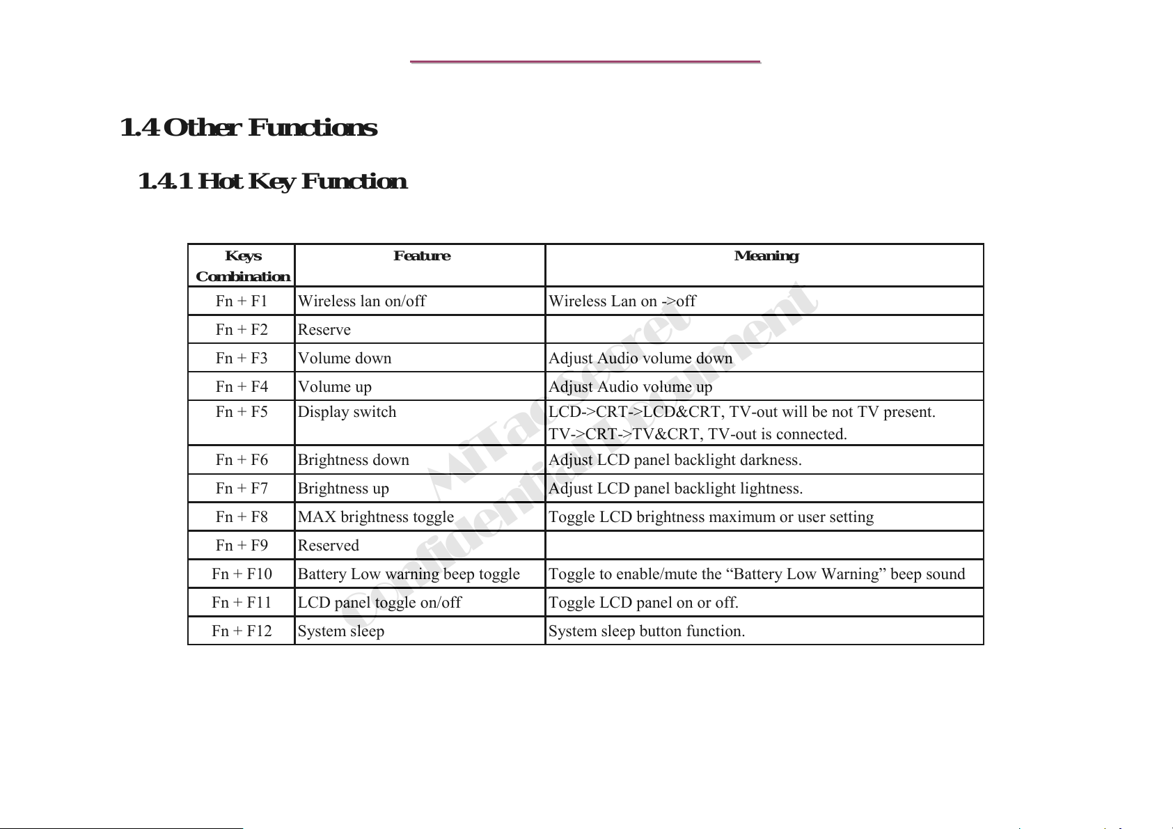
1.4 Other Functions
1.4.1 Hot Key Function
Keys Feature Meaning
Combination
Fn + F1 Wireless lan on/off Wireless Lan on ->off
Fn + F2 Reserve
Fn + F3 Volume down Adjust Audio volume down
Fn + F4 Volume up Adjust Audio volume up
Fn + F5 Display switch LCD->CRT->LCD&CRT, TV-out will be not TV present.
8399
8399
N/B Maintenance
N/B Maintenance
TV->CRT->TV&CRT, TV-out is connected.
Fn + F6 Brightness down Adjust LCD panel backlight darkness.
Fn + F7 Brightness up Adjust LCD panel backlight lightness.
Fn + F8 MAX brightness toggle Toggle LCD brightness maximum or user setting
Fn + F9 Reserved
Fn + F10 Battery Low warning beep toggle Toggle to enable/mute the “Battery Low Warning” beep sound
Fn + F11 LCD panel toggle on/off Toggle LCD panel on or off.
Fn + F12 System sleep System sleep button function.
Confidential Document
MiTac Secret
40
Page 42
8399
8399
1.4.2 Power on/off/Suspend/Resume Button
1.4.2.1 APM Mode
At APM mode, Power button is on/off system power.
1.4.2.2 ACPI Mode
At ACPI mode, power button behavior was set by windows power management control panel. You could set
“standby” or “power off” to power button function. Continue pushing power button over 4 seconds will force
system off at ACPI mode. There is no sleep button on this machine.
N/B Maintenance
N/B Maintenance
MiTac Secret
1.4.3 Lid Switch
System automatically provides a Keyboard cover state through PS2 to relative application when user closes the
Keyboard cover.
Confidential Document
1.4.4 LED Indicators
System has some status LED indicators to display system activity,.
41
Page 43

8399
8399
1.4.4.1 Three LED Indicators on Display Housing/Cover:
From left to right that indicates, AC Power/Battery Power and Battery Charger
AC Power:
This LED lights green when AC powers to the notebook, and flash (on 1 second, off 1 second) when
Suspend to DRAM is active using AC power. The LED is off when the notebook is off or powered by
batteries.
Battery Power:
This LED lights green when Battery powers to the notebook, and flash (on 1second, off 1 second) when
N/B Maintenance
N/B Maintenance
Suspend to DRAM is active using Battery power. The LED is off when the notebook is off or powered by
MiTac Secret
AC power.
Battery Charge Status:
During normal operation, this LED stays off as long as the battery is charged. When the battery charge
Confidential Document
drops to 10% of capacity, the LED lights red, flashes per 1 second and beeps per 2 second. When AC is
connected, this indicator glows green if the battery pack is fully charged or orange (amber) if the battery is
being charged. When battery charging error, it will flash orange light.
42
Page 44

8399
8399
WLAN RF Status (BTO: Wireless LAN only):
This LED indicates WLAN RF module power status. User could use Fn+F1 to enable or disable RF.
1.4.4.2 Five LED Indicators above Front Side Housing:
From left to right that indicates CD, HDD, NUM LOCK, CAPS LOCK and SCROLL LOCK.
N/B Maintenance
N/B Maintenance
1.4.5 Fan Power on/off Management
l FAN is controlled by Embedded Controller Winbond W83L950D. Thermal with hardware monitor to sense CPU
temperature and EC control fan on/off.
1.4.6 CMOS Battery
CR2032 3V 220mAh lithium battery
Confidential Document
When AC in or system main battery inside, CMOS battery will consume no power
AC or main battery not exists, CMOS battery life is at lest 10 years
Battery was put in battery holder, can be replaced.
MiTac Secret
43
Page 45
1.4.7 I/O Port
One 3 pins AC power socket
One CRT monitor
One S-Video TV out (PAL/NTSC)
Six USB 2.0 ports for all USB devices
One MODEM RJ-11 phone jack for PSTN line
One RJ-45 for LAN
Headphone out Jack
8399
8399
N/B Maintenance
N/B Maintenance
Microphone Input Jack
One Cardbus Sockets for one type II PC card extension
MiTac Secret
Confidential Document
44
Page 46
8399
8399
N/B Maintenance
N/B Maintenance
2. System View and Disassembly
2.1 System View
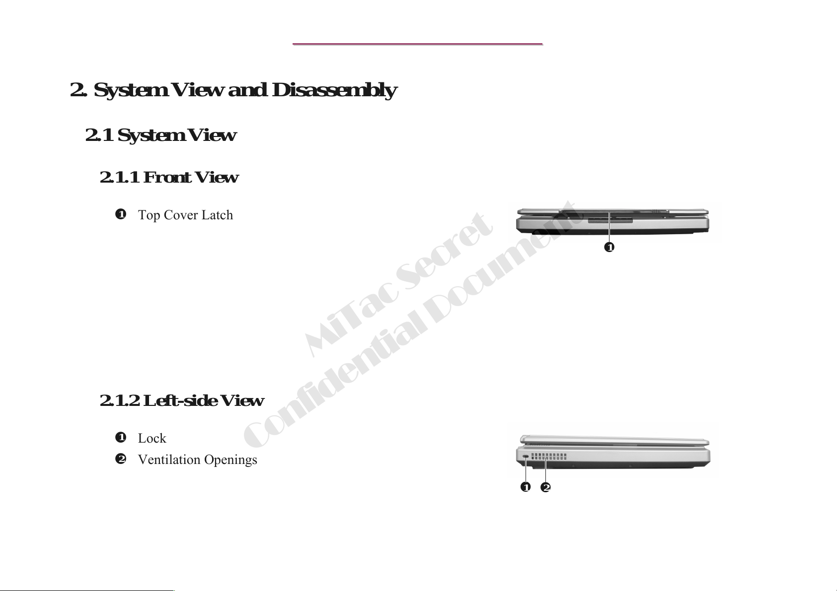
2.1.1 Front View
1
Top Cover Latch
1
2.1.2 Left-side View
1
Lock
Confidential Document
2
Ventilation Openings
MiTac Secret
1
2
45
Page 47
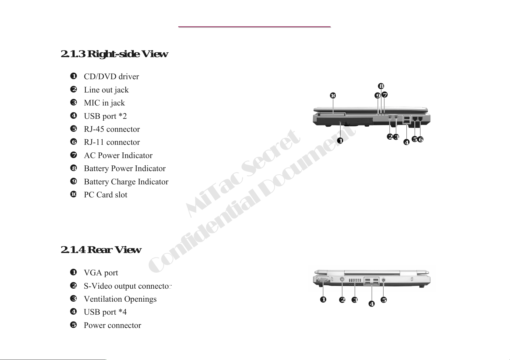
2.1.3 Right-side View
1
CD/DVD driver
2
Line out jack
3
MIC in jack
4
USB port *2
5
RJ-45 connector
6
RJ-11 connector
7
AC Power Indicator
8
Battery Power Indicator
9
Battery Charge Indicator
10
PC Card slot
8399
8399
N/B Maintenance
N/B Maintenance
10
1
9
8
7
2
3
4
5
6
2.1.4 Rear View
1
VGA port
2
S-Video output connector
3
Ventilation Openings
4
USB port *4
5
Power connector
MiTac Secret
Confidential Document
1
2
3
4
5
46
Page 48
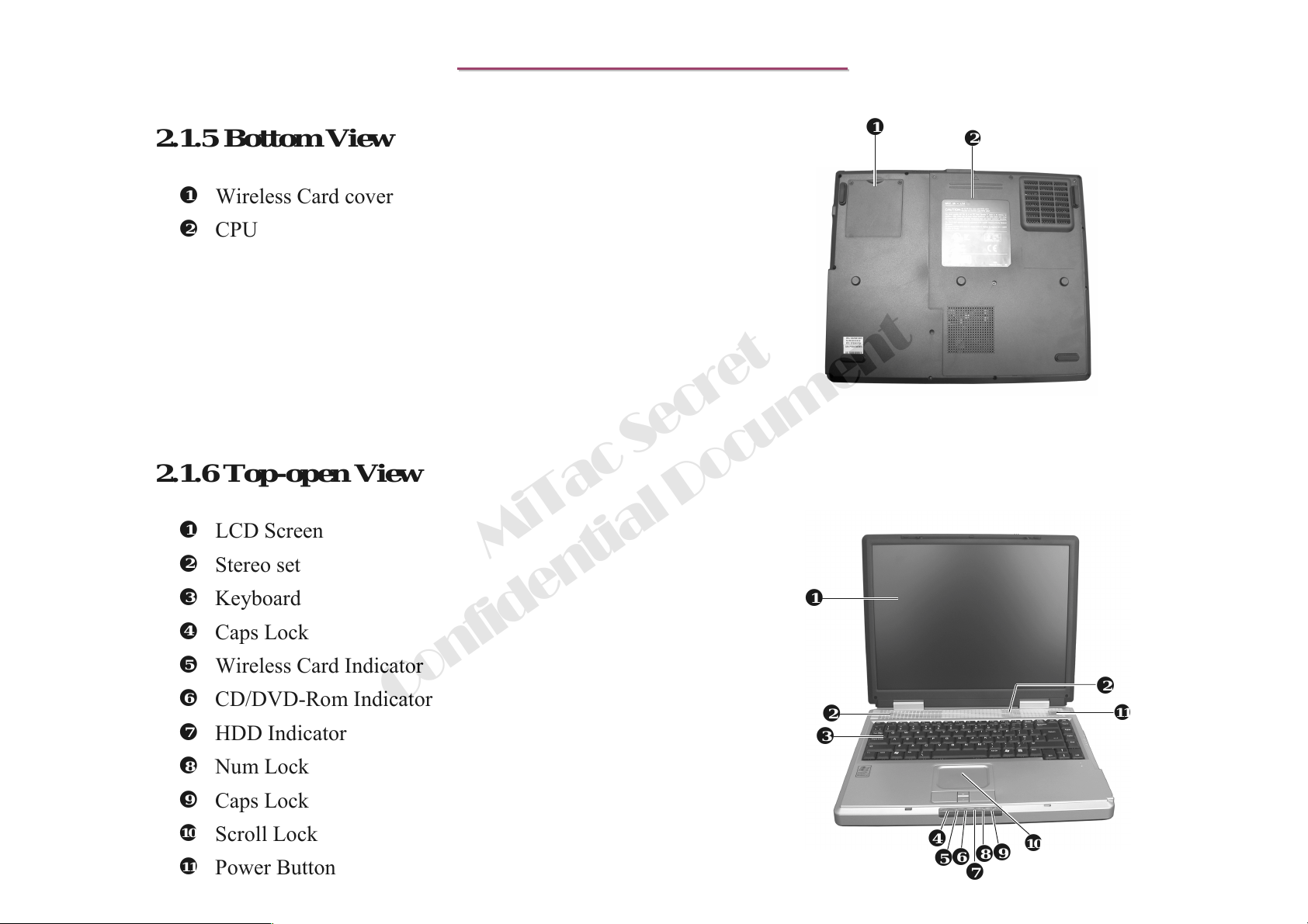
2.1.5 Bottom View
1
Wireless Card cover
2
CPU
2.1.6 Top-open View
8399
8399
N/B Maintenance
N/B Maintenance
1
2
1
LCD Screen
2
Stereo set
3
Keyboard
4
Caps Lock
5
Wireless Card Indicator
6
CD/DVD-Rom Indicator
7
HDD Indicator
8
Num Lock
9
Caps Lock
10
Scroll Lock
11
Power Button
Confidential Document
MiTac Secret
1
2
3
4
2
11
10
9
8
6
5
7
47
Page 49
8399
8399
N/B Maintenance
N/B Maintenance
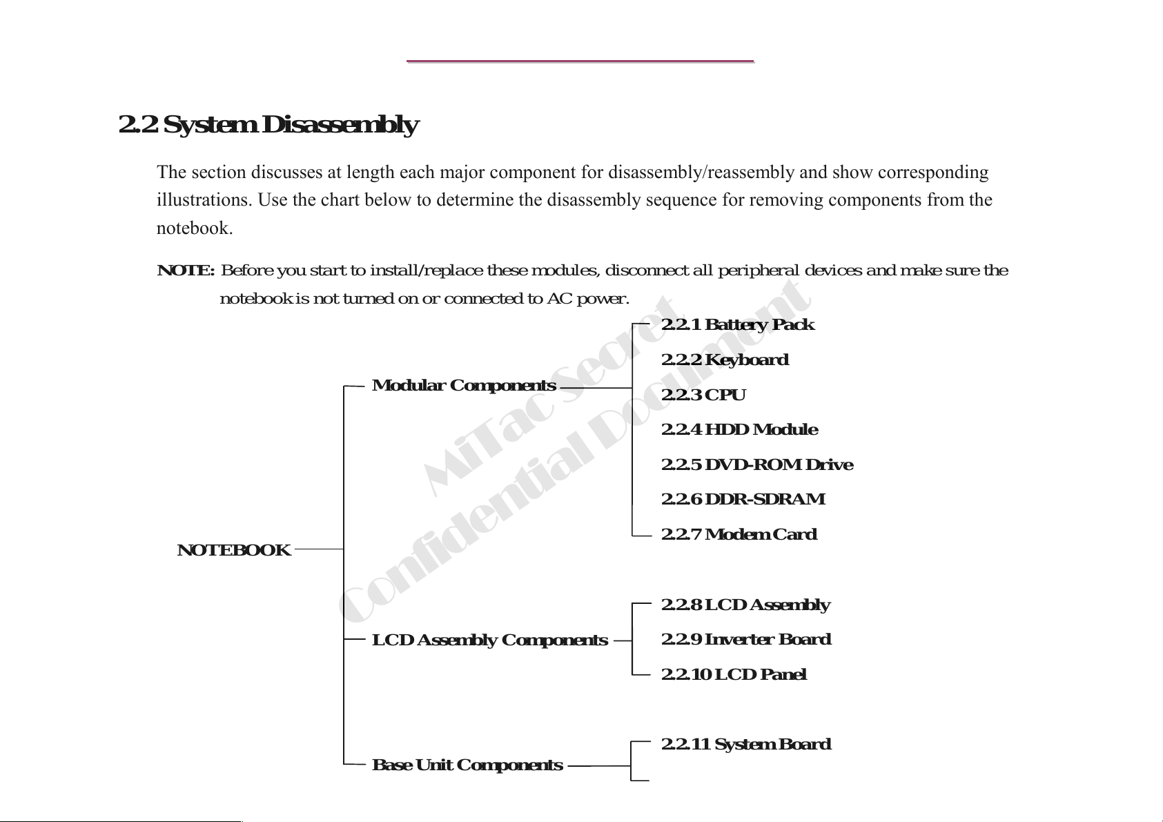
2.2 System Disassembly
The section discusses at length each major component for disassembly/reassembly and show corresponding
illustrations. Use the chart below to determine the disassembly sequence for removing components from the
notebook.
NOTE: Before you start to install/replace these modules, disconnect all peripheral devices and make sure the
notebook is not turned on or connected to AC power.
2.2.1 Battery Pack
2.2.2 Keyboard
NOTEBOOK
Modular Components
MiTac Secret
2.2.3 CPU
2.2.4 HDD Module
2.2.5 DVD-ROM Drive
2.2.6 DDR-SDRAM
2.2.7 Modem Card
2.2.8 LCD Assem bly
Confidential Document
LCD Assembly Components
Base Unit Components
2.2.9 Inverter Board
2.2.10 LCD Panel
2.2.11 System Board
2.2.12 Touch Pad
48
Page 50
8399
8399
N/B Maintenance
N/B Maintenance
2.2.1 Battery Pack
Disassembly
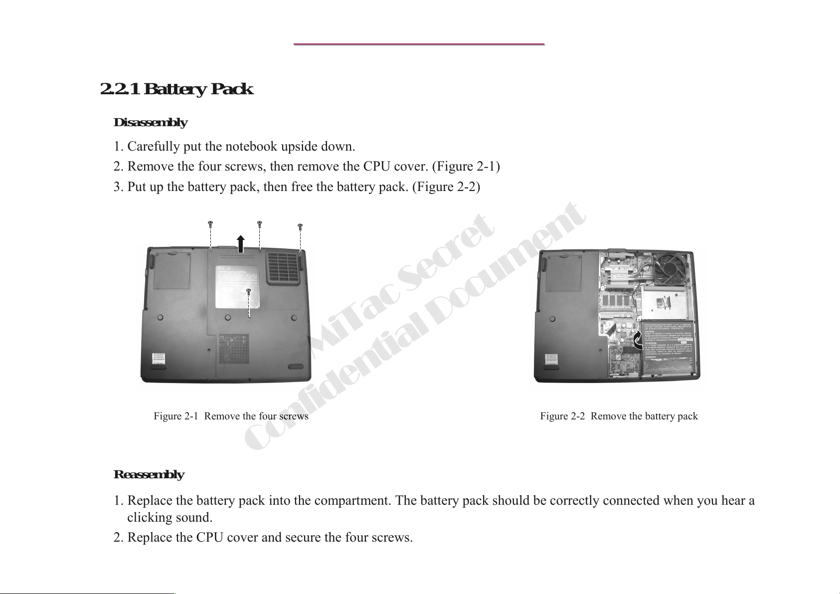
1. Carefully put the notebook upside down.
2. Remove the four screws, then remove the CPU cover. (Figure 2-1)
3. Put up the battery pack, then free the battery pack. (Figure 2-2)
MiTac Secret
Figure 2-1 Remove the four screws
Figure 2-2 Remove the battery pack
Confidential Document
Reassembly
1. Replace the battery pack into the compartment. The battery pack should be correctly connected when you hear a
clicking sound.
2. Replace the CPU cover and secure the four screws.
49
Page 51
8399
8399
2.2.2 Keyboard
Disassembly
1. Remove the battery pack. (Refer to section 2.2.1 Disassembly)
2. Open the top cover.
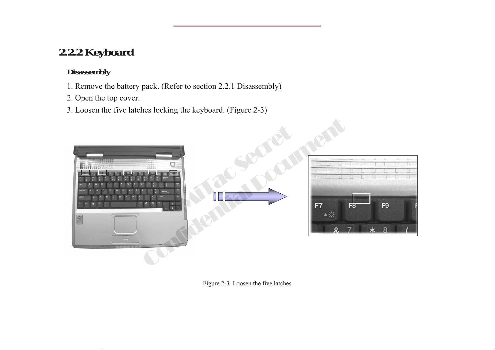
3. Loosen the five latches locking the keyboard. (Figure 2-3)
N/B Maintenance
N/B Maintenance
MiTac Secret
Confidential Document
Figure 2-3 Loosen the five latches
50
Page 52
8399
8399
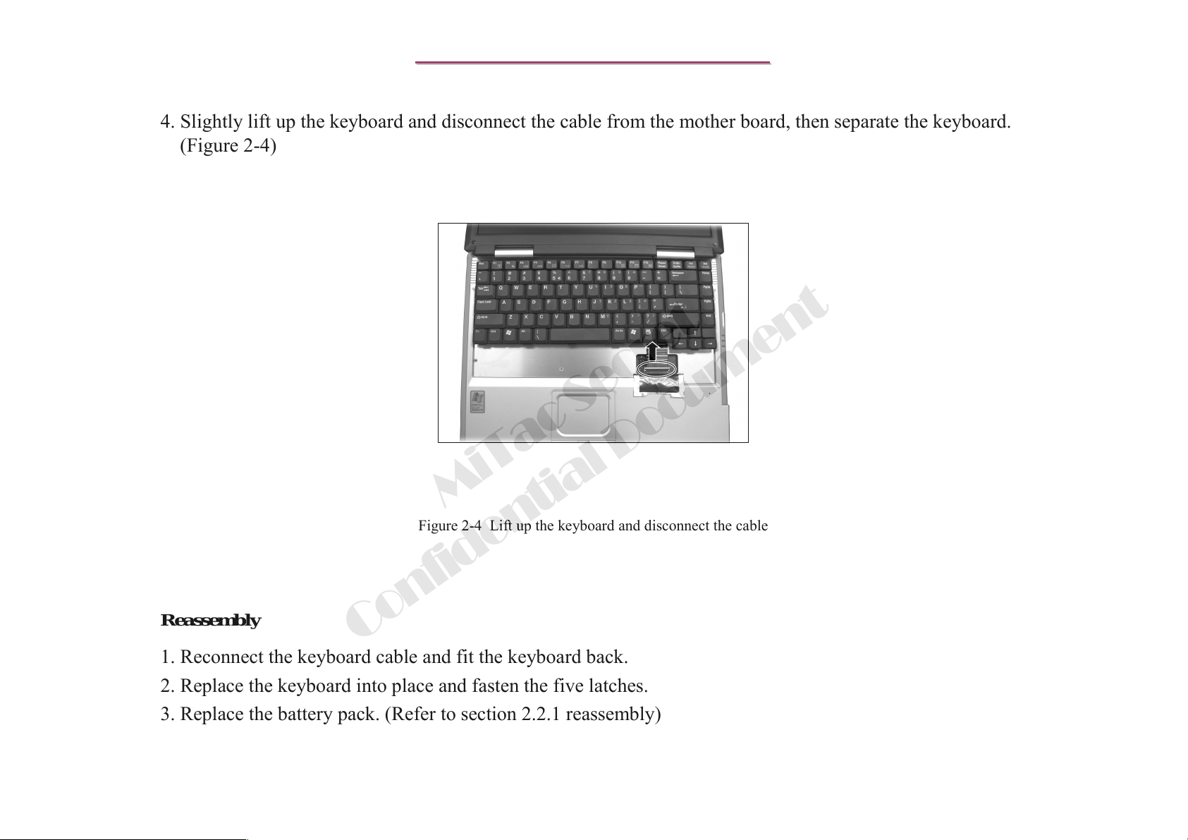
4. Slightly lift up the keyboard and disconnect the cable from the mother board, then separate the keyboard.
(Figure 2-4)
N/B Maintenance
N/B Maintenance
MiTac Secret
Figure 2-4 Lift up the keyboard and disconnect the cable
Reassembly
Confidential Document
1. Reconnect the keyboard cable and fit the keyboard back.
2. Replace the keyboard into place and fasten the five latches.
3. Replace the battery pack. (Refer to section 2.2.1 reassembly)
51
Page 53
8399
8399
2.2.3 CPU
Disassembly
1. Remove the battery pack. (Refer to section 2.2.1 Disassembly)
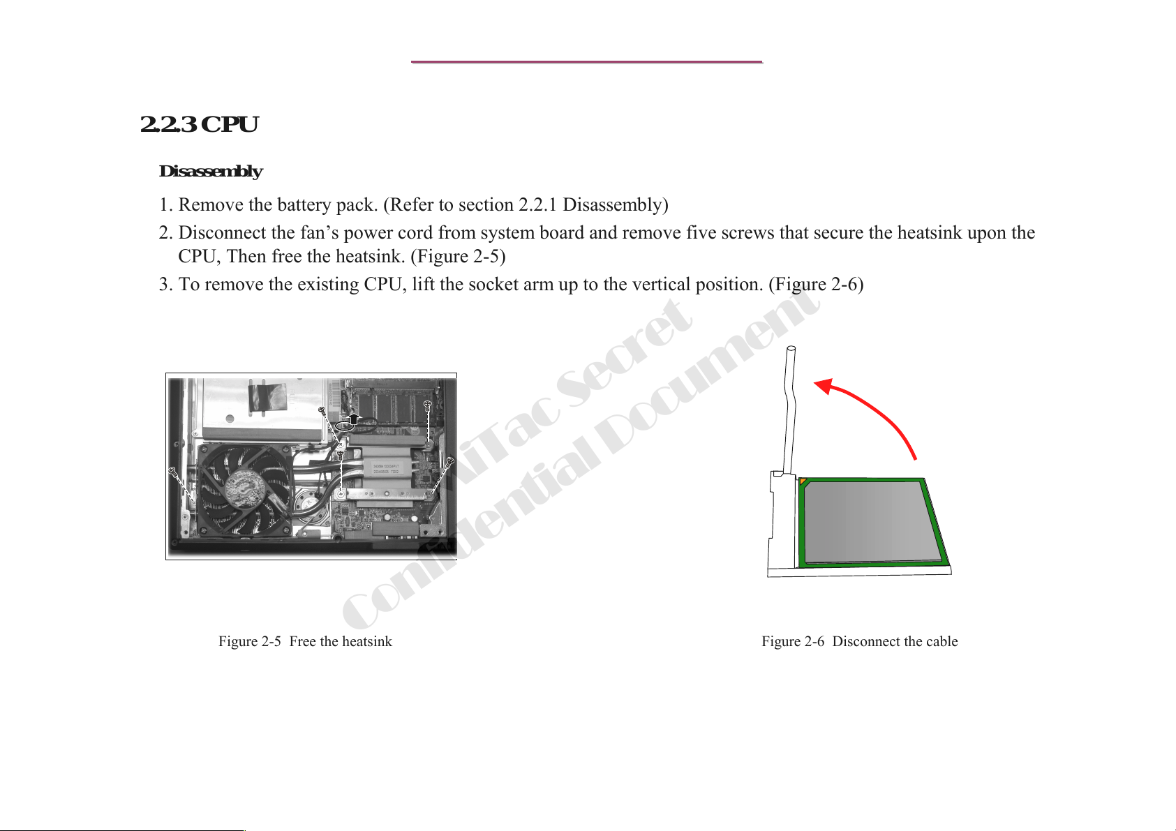
2. Disconnect the fan’s power cord from system board and remove five screws that secure the heatsink upon the
CPU, Then free the heatsink. (Figure 2-5)
3. To remove the existing CPU, lift the socket arm up to the vertical position. (Figure 2-6)
N/B Maintenance
N/B Maintenance
MiTac Secret
Figure 2-5 Free the heatsink Figure 2-6 Disconnect the cable
Confidential Document
52
Page 54
8399
8399
Reassembly
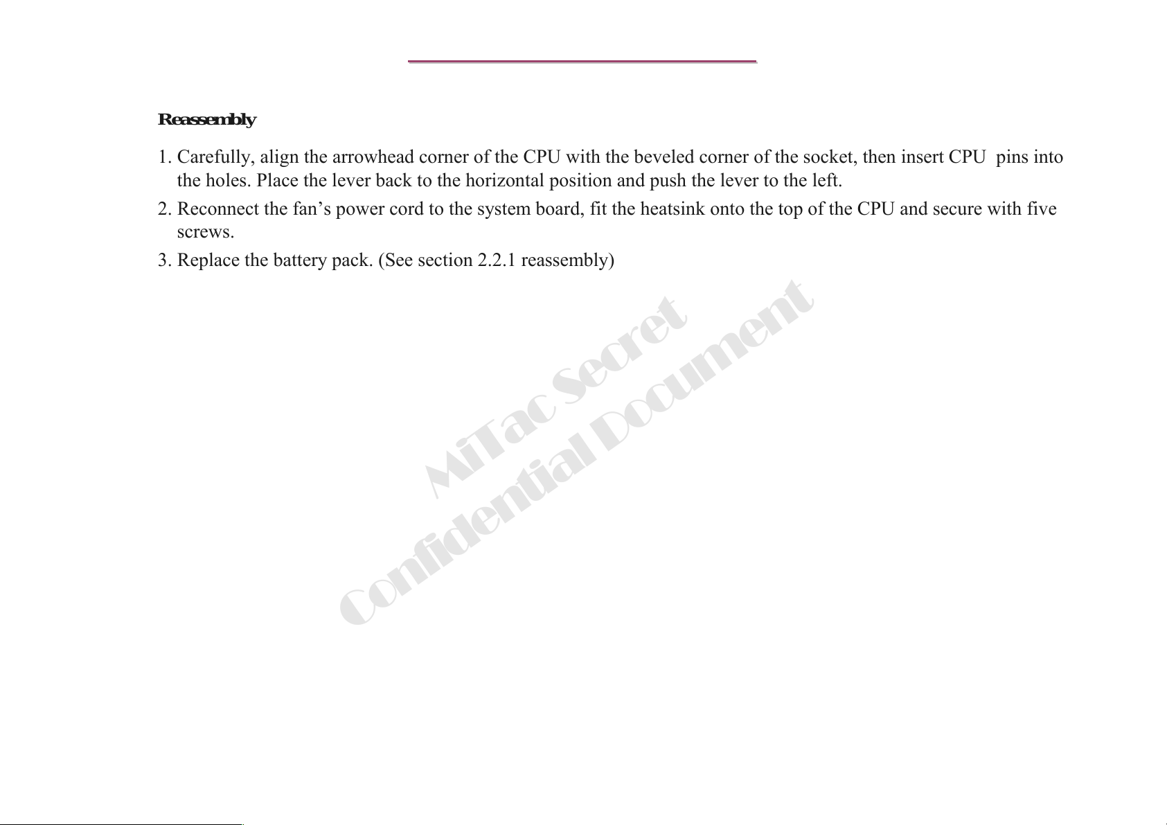
1. Carefully, align the arrowhead corner of the CPU with the beveled corner of the socket, then insert CPU pins into
the holes. Place the lever back to the horizontal position and push the lever to the left.
2. Reconnect the fan’s power cord to the system board, fit the heatsink onto the top of the CPU and secure with five
screws.
N/B Maintenance
N/B Maintenance
3. Replace the battery pack. (See section 2.2.1 reassembly)
MiTac Secret
Confidential Document
CPU socket stopper
53
Page 55
8399
8399
N/B Maintenance
N/B Maintenance
2.2.4 HDD Module
Disassembly
1. Carefully put the notebook upside down. Remove the battery pack. (Refer to section 2.2.1 Disassembly)
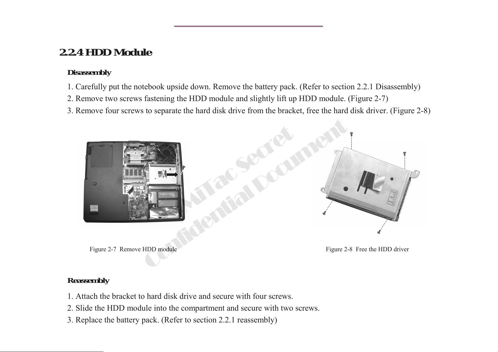
2. Remove two screws fastening the HDD module and slightly lift up HDD module. (Figure 2-7)
3. Remove four screws to separate the hard disk drive from the bracket, free the hard disk driver. (Figure 2-8)
MiTac Secret
Confidential Document
Reassembly
1. Attach the bracket to hard disk drive and secure with four screws.
2. Slide the HDD module into the compartment and secure with two screws.
3. Replace the battery pack. (Refer to section 2.2.1 reassembly)
Figure 2-8 Free the HDD driverFigure 2-7 Remove HDD module
54
Page 56
8399
8399
N/B Maintenance
N/B Maintenance
2.2.5 CD/DVD-ROM Drive
DisassemblyDisassembly
1. Carefully put the notebook upside down. Remove the battery pack. (Refer to section 2.2.1 Disassembly)
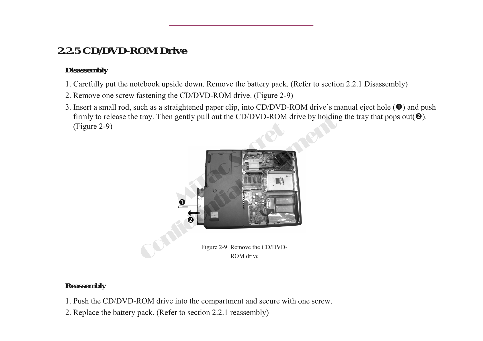
2. Remove one screw fastening the CD/DVD-ROM drive. (Figure 2-9)
3. Insert a small rod, such as a straightened paper clip, into CD/DVD-ROM drive’s manual eject hole () and push
firmly to release the tray. Then gently pull out the CD/DVD-ROM drive by holding the tray that pops out().
(Figure 2-9)
MiTac Secret
Figure 2-9 Remove the CD/DVD-
Confidential Document
Reassembly
1. Push the CD/DVD-ROM drive into the compartment and secure with one screw.
2. Replace the battery pack. (Refer to section 2.2.1 reassembly)
ROM drive
55
Page 57
8399
8399
2.2.6 DDR-SDRAM
DisassemblyDisassembly
1. Carefully put the notebook upside down. Remove the battery pack. (Refer to section 2.2.1 Disassembly)
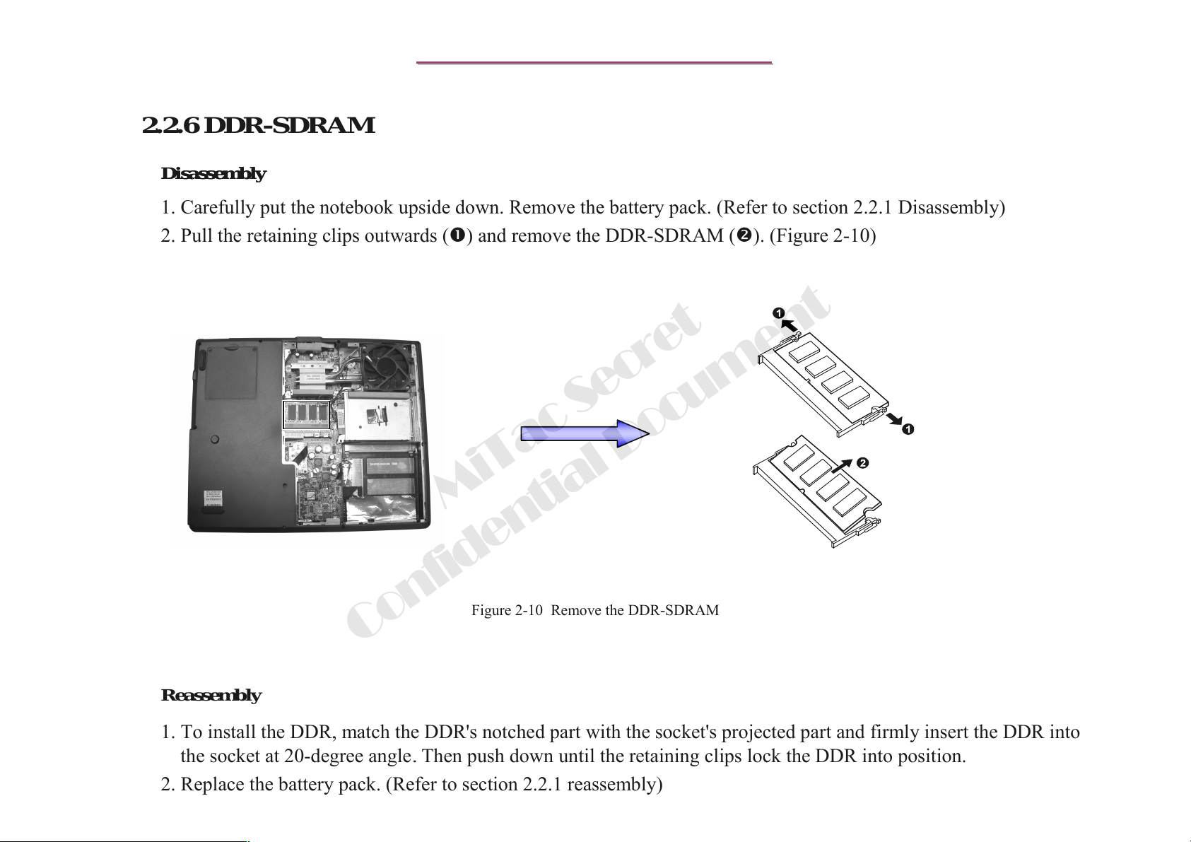
2. Pull the retaining clips outwards () and remove the DDR-SDRAM (). (Figure 2-10)
N/B Maintenance
N/B Maintenance
MiTac Secret
Figure 2-10 Remove the DDR-SDRAM
Confidential Document
Reassembly
1. To install the DDR, match the DDR's notched part with the socket's projected part and firmly insert the DDR into
the socket at 20-degree angle. Then push down until the retaining clips lock the DDR into position.
2. Replace the battery pack. (Refer to section 2.2.1 reassembly)
56
Page 58
8399
8399
N/B Maintenance
N/B Maintenance
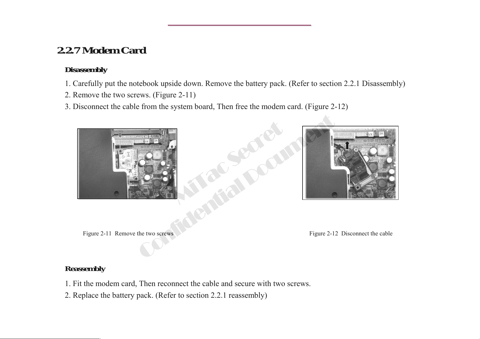
2.2.7 Modem Card
DisassemblyDisassembly
1. Carefully put the notebook upside down. Remove the battery pack. (Refer to section 2.2.1 Disassembly)
2. Remove the two screws. (Figure 2-11)
3. Disconnect the cable from the system board, Then free the modem card. (Figure 2-12)
MiTac Secret
Figure 2-11 Remove the two screws
Confidential Document
Reassembly
1. Fit the modem card, Then reconnect the cable and secure with two screws.
2. Replace the battery pack. (Refer to section 2.2.1 reassembly)
Figure 2-12 Disconnect the cable
57
Page 59
8399
8399
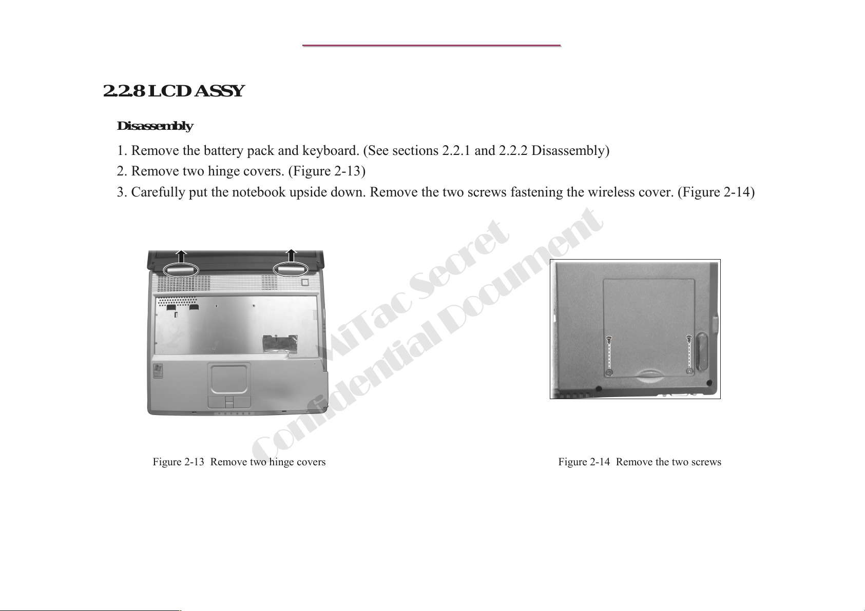
2.2.8 LCD ASSY
Disassembly
1. Remove the battery pack and keyboard. (See sections 2.2.1 and 2.2.2 Disassembly)
2. Remove two hinge covers. (Figure 2-13)
3. Carefully put the notebook upside down. Remove the two screws fastening the wireless cover. (Figure 2-14)
N/B Maintenance
N/B Maintenance
Figure 2-13 Remove two hinge covers
Confidential Document
MiTac Secret
Figure 2-14 Remove the two screws
58
Page 60
8399
8399
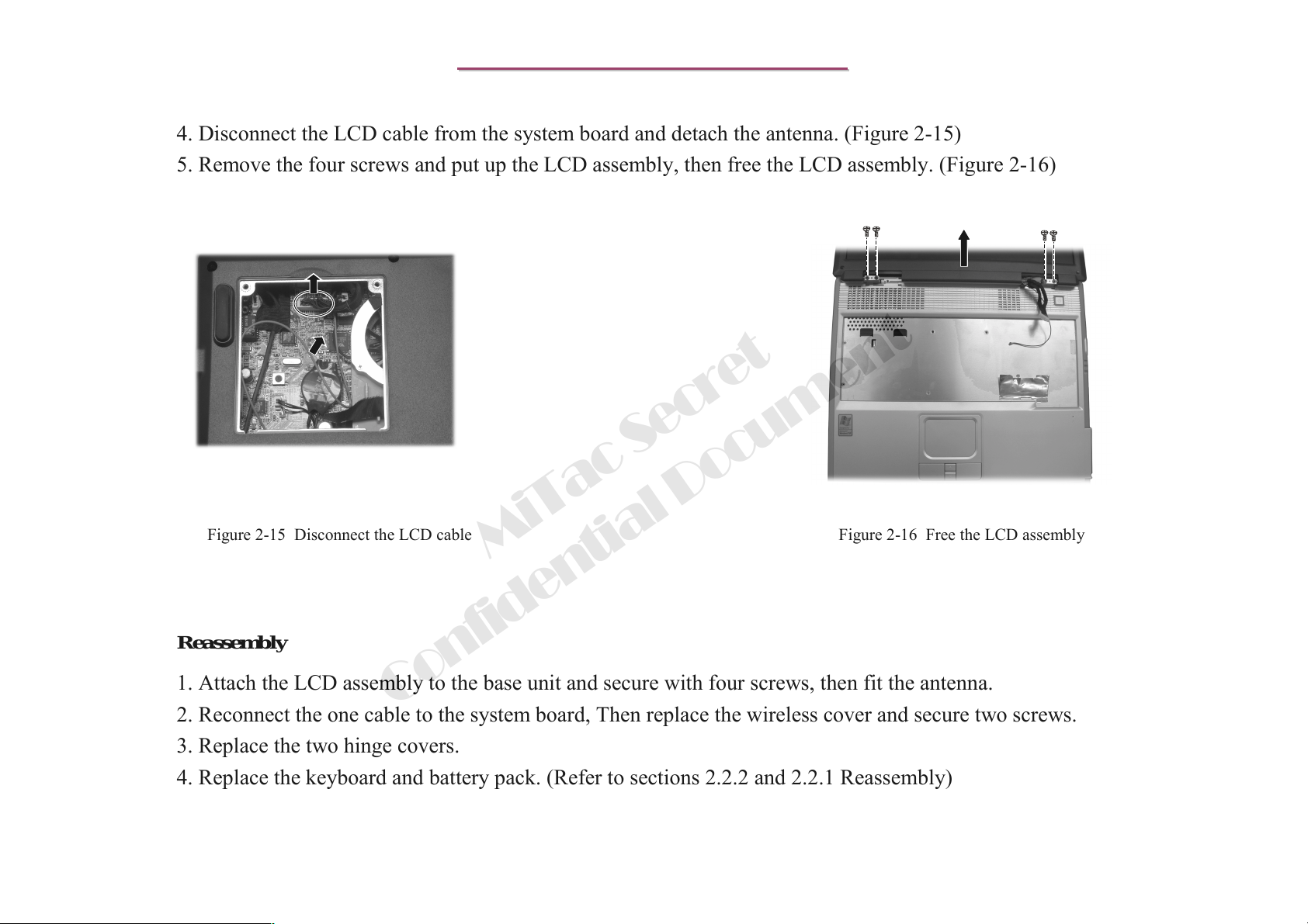
4. Disconnect the LCD cable from the system board and detach the antenna. (Figure 2-15)
5. Remove the four screws and put up the LCD assembly, then free the LCD assembly. (Figure 2-16)
N/B Maintenance
N/B Maintenance
Figure 2-15 Disconnect the LCD cable
Figure 2-16 Free the LCD assembly
MiTac Secret
Reassembly
1. Attach the LCD assembly to the base unit and secure with four screws, then fit the antenna.
Confidential Document
2. Reconnect the one cable to the system board, Then replace the wireless cover and secure two screws.
3. Replace the two hinge covers.
4. Replace the keyboard and battery pack. (Refer to sections 2.2.2 and 2.2.1 Reassembly)
59
Page 61
8399
8399
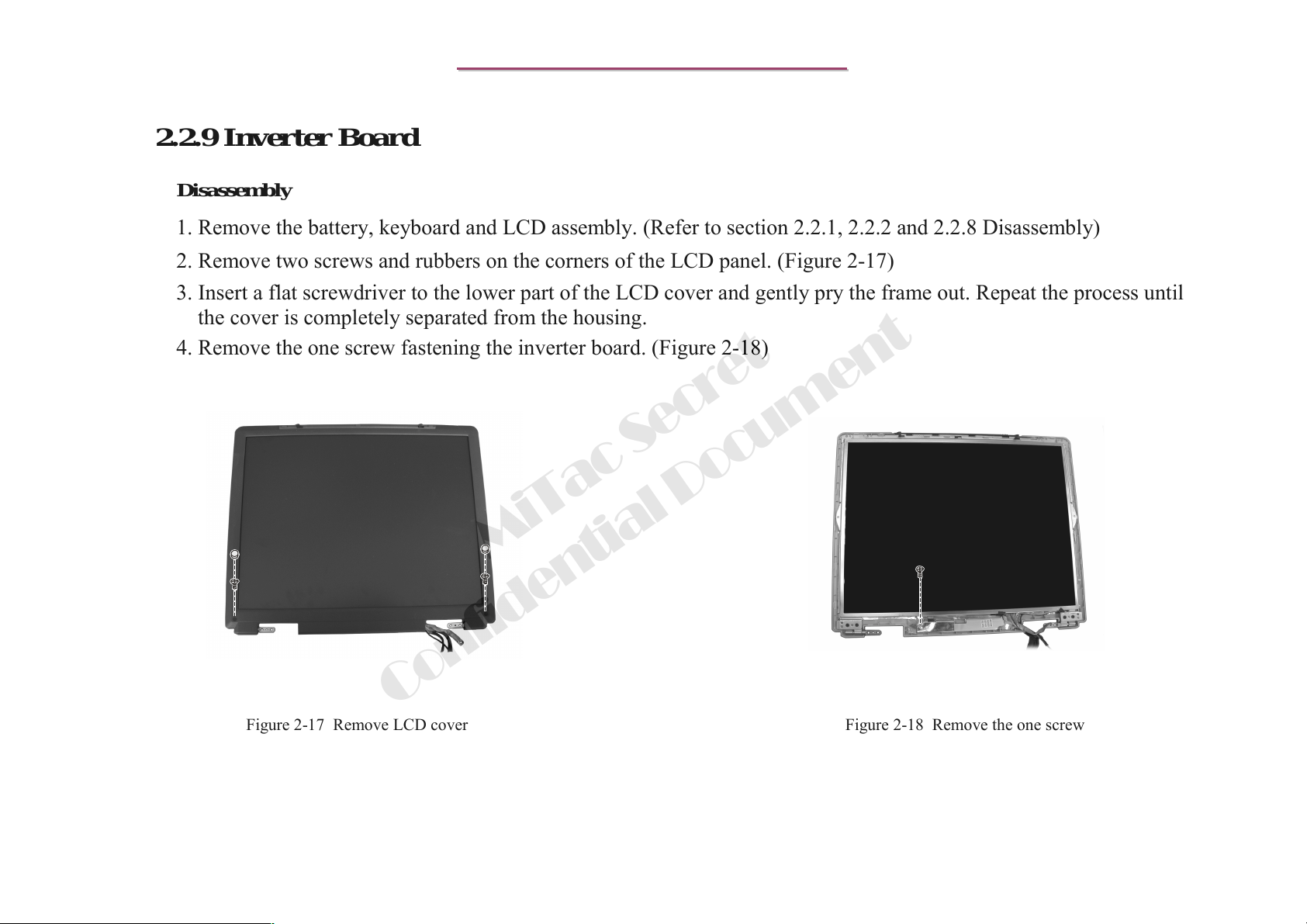
2.2.9 Inverter Board
Disassembly
1. Remove the battery, keyboard and LCD assembly. (Refer to section 2.2.1, 2.2.2 and 2.2.8 Disassembly)
2. Remove two screws and rubbers on the corners of the LCD panel. (Figure 2-17)
3. Insert a flat screwdriver to the lower part of the LCD cover and gently pry the frame out. Repeat the process until
the cover is completely separated from the housing.
4. Remove the one screw fastening the inverter board. (Figure 2-18)
N/B Maintenance
N/B Maintenance
MiTac Secret
Confidential Document
Figure 2-18 Remove the one screwFigure 2-17 Remove LCD cover
60
Page 62
8399
8399
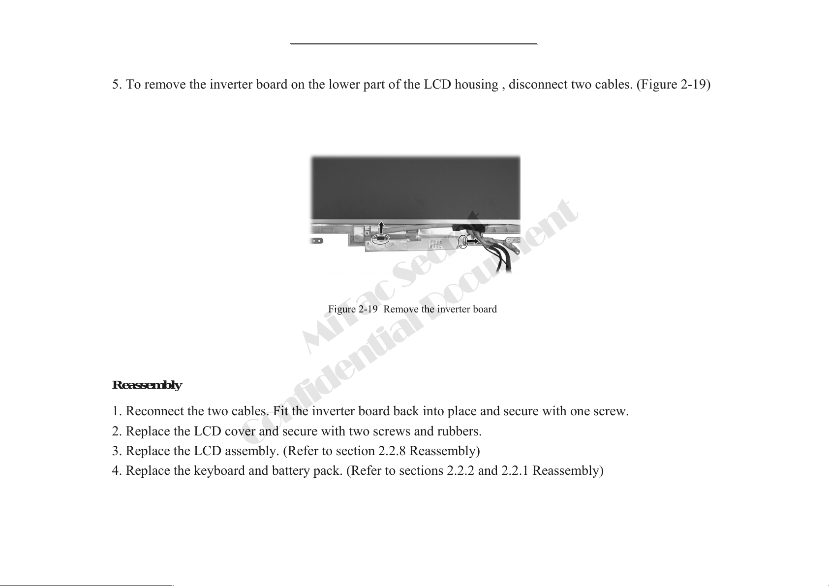
5. To remove the inverter board on the lower part of the LCD housing , disconnect two cables. (Figure 2-19)
N/B Maintenance
N/B Maintenance
Figure 2-19 Remove the inverter board
MiTac Secret
Reassembly
1. Reconnect the two cables. Fit the inverter board back into place and secure with one screw.
2. Replace the LCD cover and secure with two screws and rubbers.
3. Replace the LCD assembly. (Refer to section 2.2.8 Reassembly)
4. Replace the keyboard and battery pack. (Refer to sections 2.2.2 and 2.2.1 Reassembly)
Confidential Document
61
Page 63
8399
8399
N/B Maintenance
N/B Maintenance
2.2.10 LCD Panel
Disassembly
1. Remove the battery, keyboard and LCD assembly. (Refer to sections 2.2.1, 2.2.2 and 2.2.8 Disassembly)
2. Remove the LCD cover. (Refer for two steps 2,3 of section 2.2.9 Disassembly)
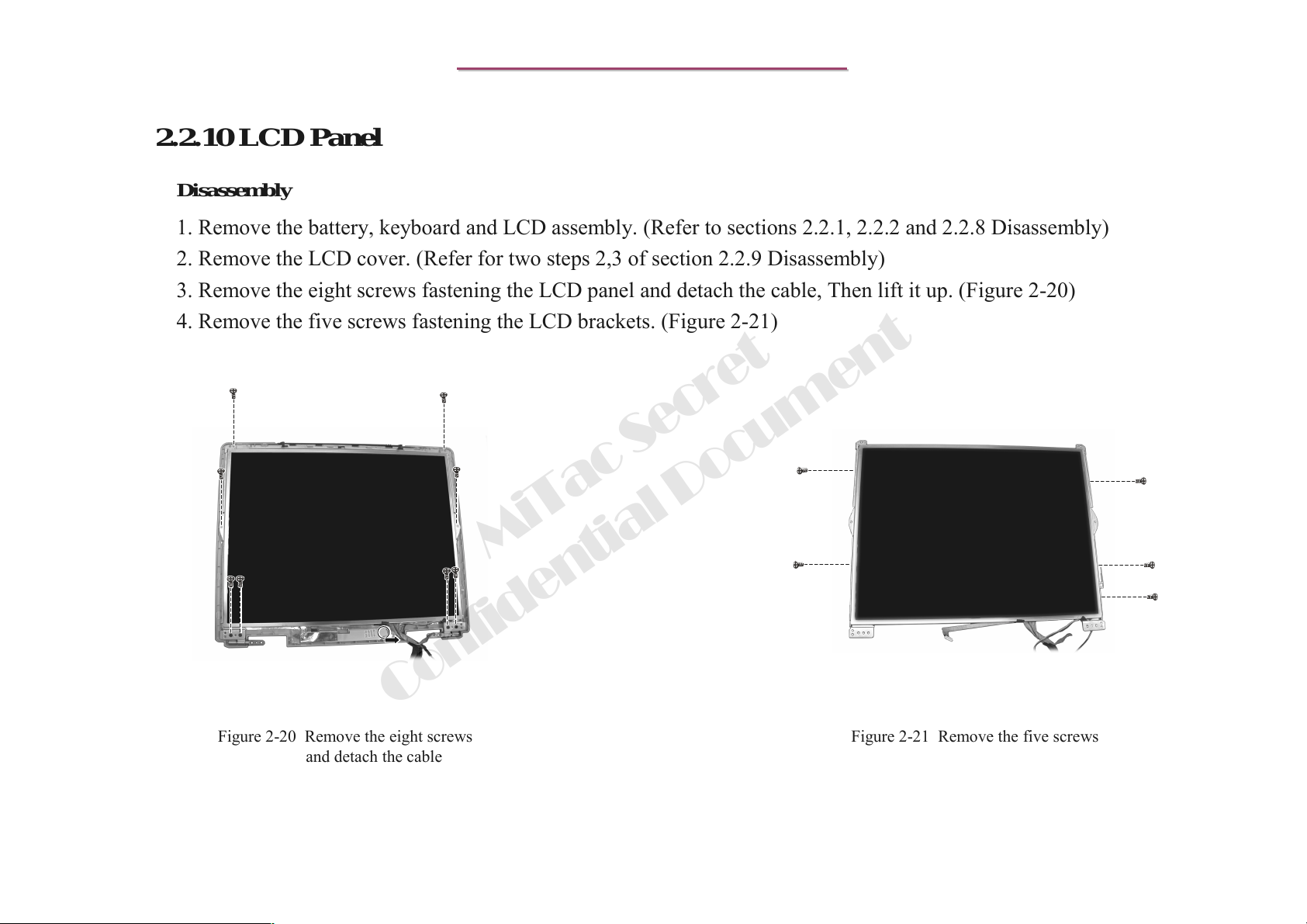
3. Remove the eight screws fastening the LCD panel and detach the cable, Then lift it up. (Figure 2-20)
4. Remove the five screws fastening the LCD brackets. (Figure 2-21)
Confidential Document
Figure 2-20 Remove the eight screws
and detach the cable
MiTac Secret
Figure 2-21 Remove the five screws
62
Page 64
8399
8399
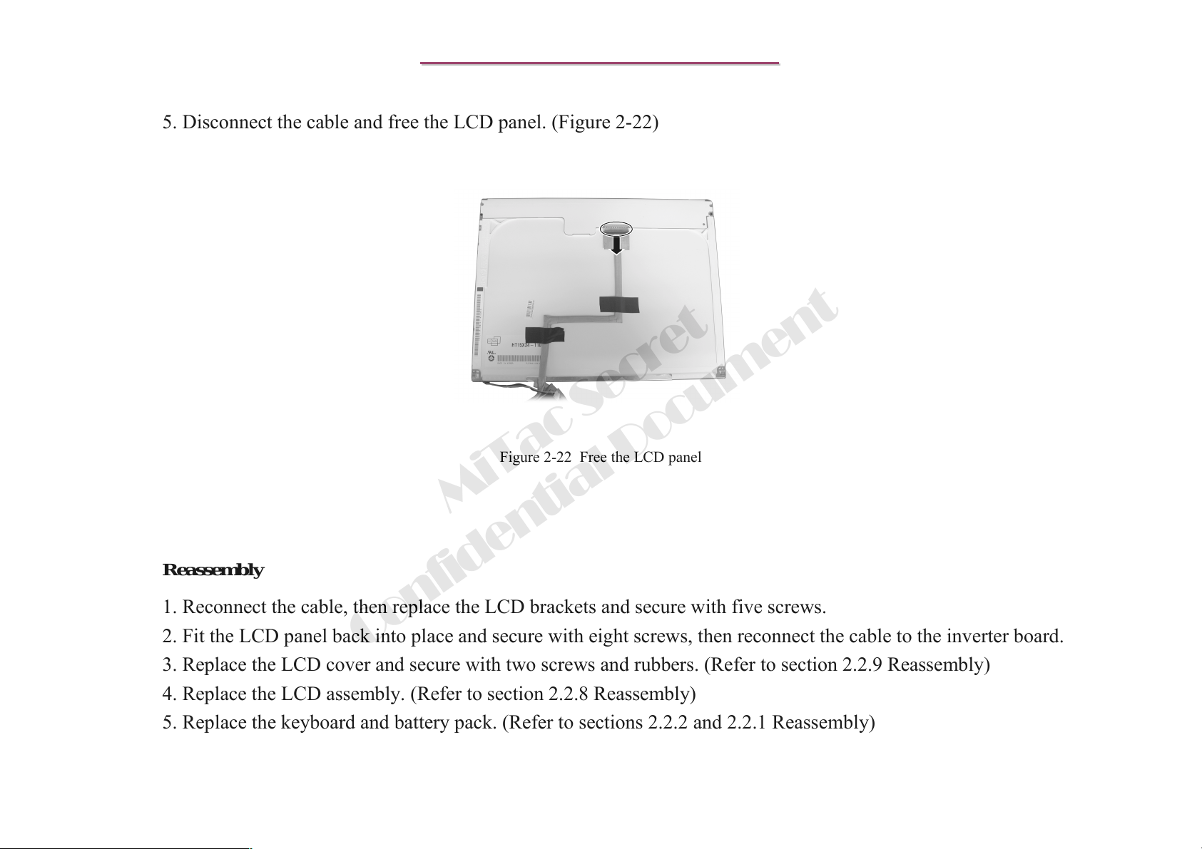
5. Disconnect the cable and free the LCD panel. (Figure 2-22)
N/B Maintenance
N/B Maintenance
Figure 2-22 Free the LCD panel
MiTac Secret
Reassembly
1. Reconnect the cable, then replace the LCD brackets and secure with five screws.
2. Fit the LCD panel back into place and secure with eight screws, then reconnect the cable to the inverter board.
3. Replace the LCD cover and secure with two screws and rubbers. (Refer to section 2.2.9 Reassembly)
4. Replace the LCD assembly. (Refer to section 2.2.8 Reassembly)
5. Replace the keyboard and battery pack. (Refer to sections 2.2.2 and 2.2.1 Reassembly)
Confidential Document
63
Page 65
8399
8399
2.2.11 System Board
Disassembly
1. Remove the battery, keyboard, CPU, hard disk drive, CD/DVD-ROM drive, DDR-SDRAM, modem card and
LCD assembly. (Refer to sections 2.2.1, 2.2.2, 2.2.3, 2.2.4, 2.2.5, 2.2.6, 2.2.7 and 2.2.8 Disassembly)
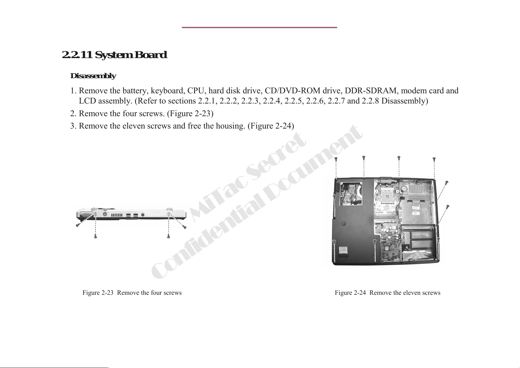
2. Remove the four screws. (Figure 2-23)
3. Remove the eleven screws and free the housing. (Figure 2-24)
N/B Maintenance
N/B Maintenance
MiTac Secret
Confidential Document
Figure 2-24 Remove the eleven screwsFigure 2-23 Remove the four screws
64
Page 66
8399
8399
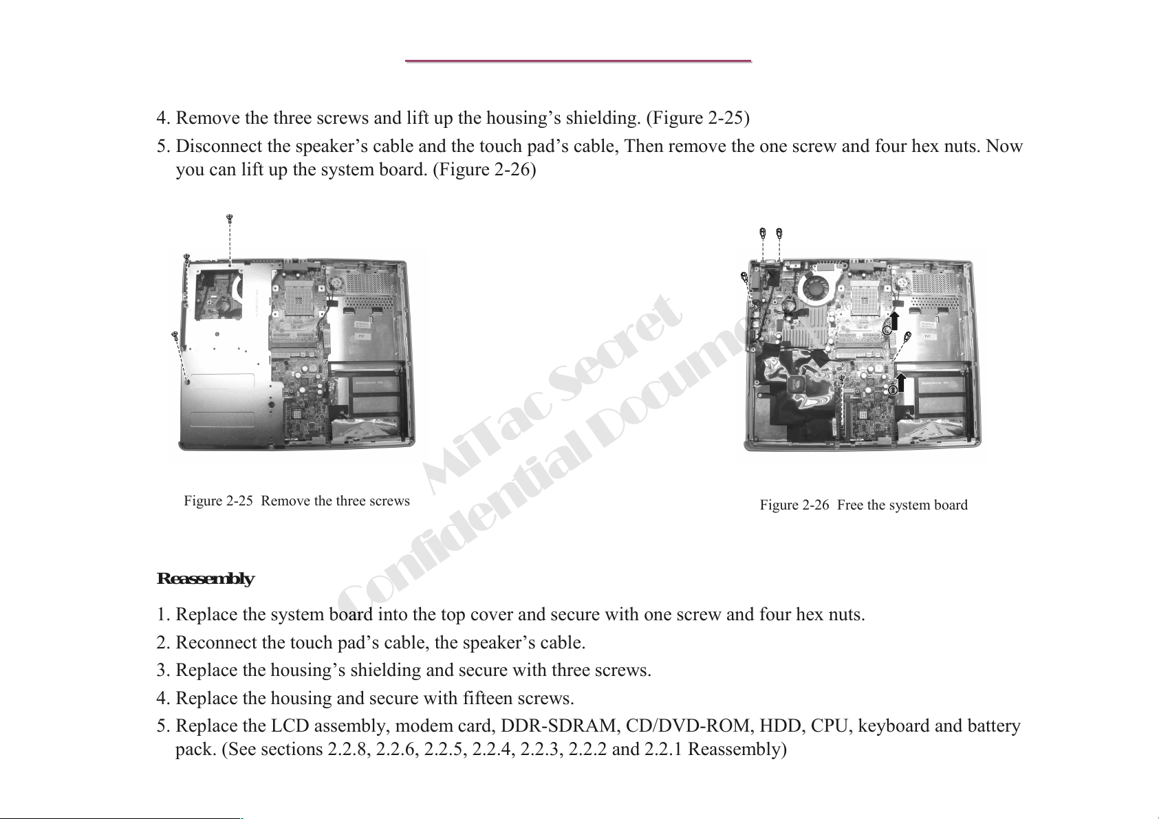
4. Remove the three screws and lift up the housing’s shielding. (Figure 2-25)
5. Disconnect the speaker’s cable and the touch pad’s cable, Then remove the one screw and four hex nuts. Now
you can lift up the system board. (Figure 2-26)
N/B Maintenance
N/B Maintenance
Figure 2-25 Remove the three screws
Reassembly
1. Replace the system board into the top cover and secure with one screw and four hex nuts.
2. Reconnect the touch pad’s cable, the speaker’s cable.
3. Replace the housing’s shielding and secure with three screws.
4. Replace the housing and secure with fifteen screws.
5. Replace the LCD assembly, modem card, DDR-SDRAM, CD/DVD-ROM, HDD, CPU, keyboard and battery
pack. (See sections 2.2.8, 2.2.6, 2.2.5, 2.2.4, 2.2.3, 2.2.2 and 2.2.1 Reassembly)
Confidential Document
MiTac Secret
Figure 2-26 Free the system board
65
Page 67
8399
8399
2.2.12 Touch Pad
Disassembly
1. Remove the system board. (See section 2.2.11 Disassembly)
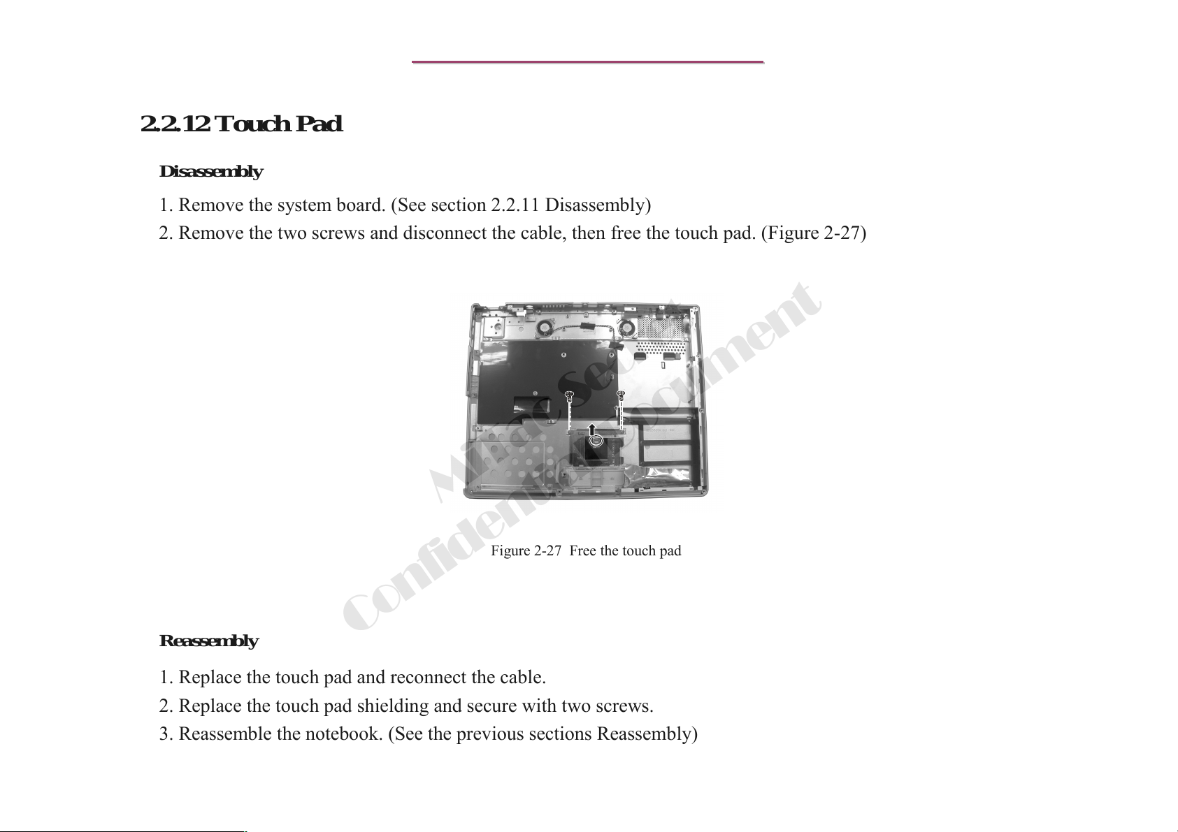
2. Remove the two screws and disconnect the cable, then free the touch pad. (Figure 2-27)
N/B Maintenance
N/B Maintenance
MiTac Secret
Figure 2-27 Free the touch pad
Reassembly
1. Replace the touch pad and reconnect the cable.
2. Replace the touch pad shielding and secure with two screws.
3. Reassemble the notebook. (See the previous sections Reassembly)
Confidential Document
66
Page 68
8399
8399
N/B Maintenance
N/B Maintenance
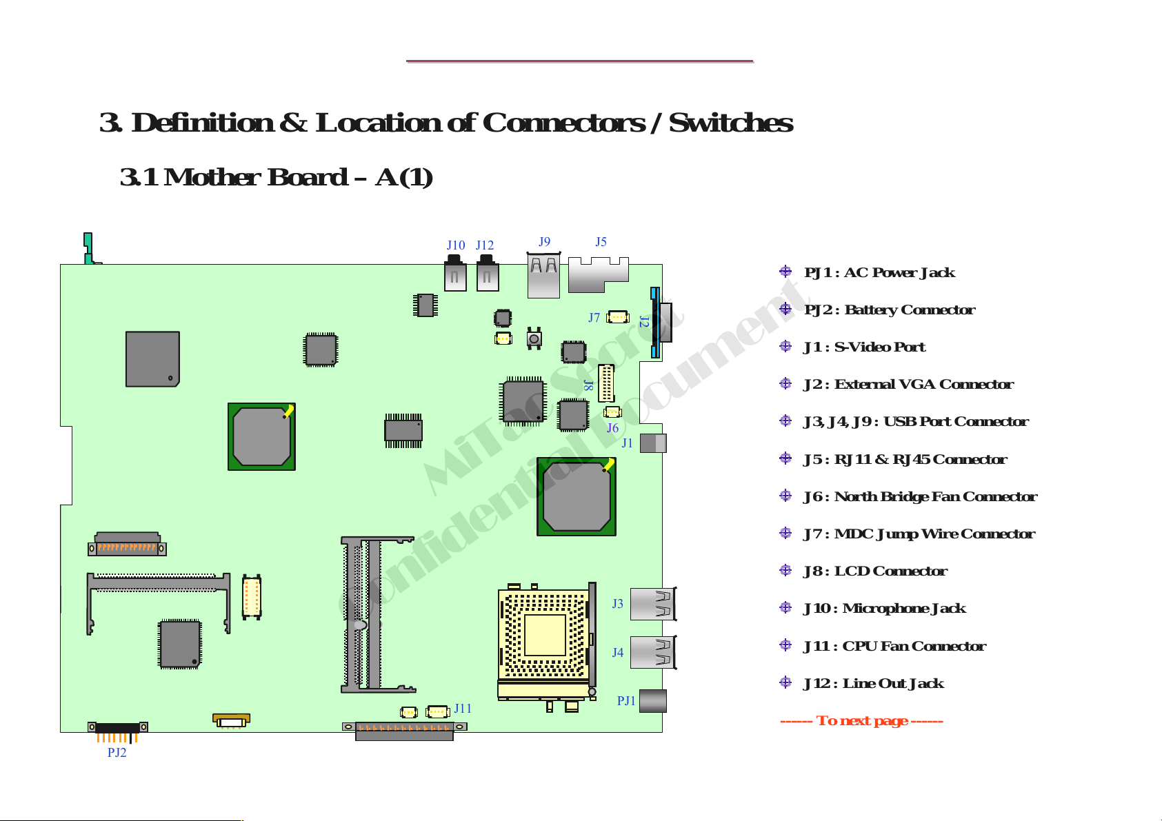
3. Definition & Location of Connectors / Switches
3.1 Mother Board – A(1)
J509
J10 J12
MiTac Secret
J9 J5
J7
J8
J6
J3
J1
J2
PJ1 : AC Power Jack
PJ2 : Battery Connector
J1 : S-Video Port
J2 : External VGA Connector
J3, J4, J9 : USB Port Connector
J5 : RJ11 & RJ45 Connector
J6 : North Bridge Fan Connector
J7 : MDC Jump Wire Connecto r
J8 : LCD Connector
J10 : Microphone Jack
Confidential Document
J4
J11 : CPU Fan Connec tor
PJ2
J11
J12 : Line Out Jack
PJ1
------ To next page ------
67
Page 69
8399
8399
N/B Maintenance
N/B Maintenance
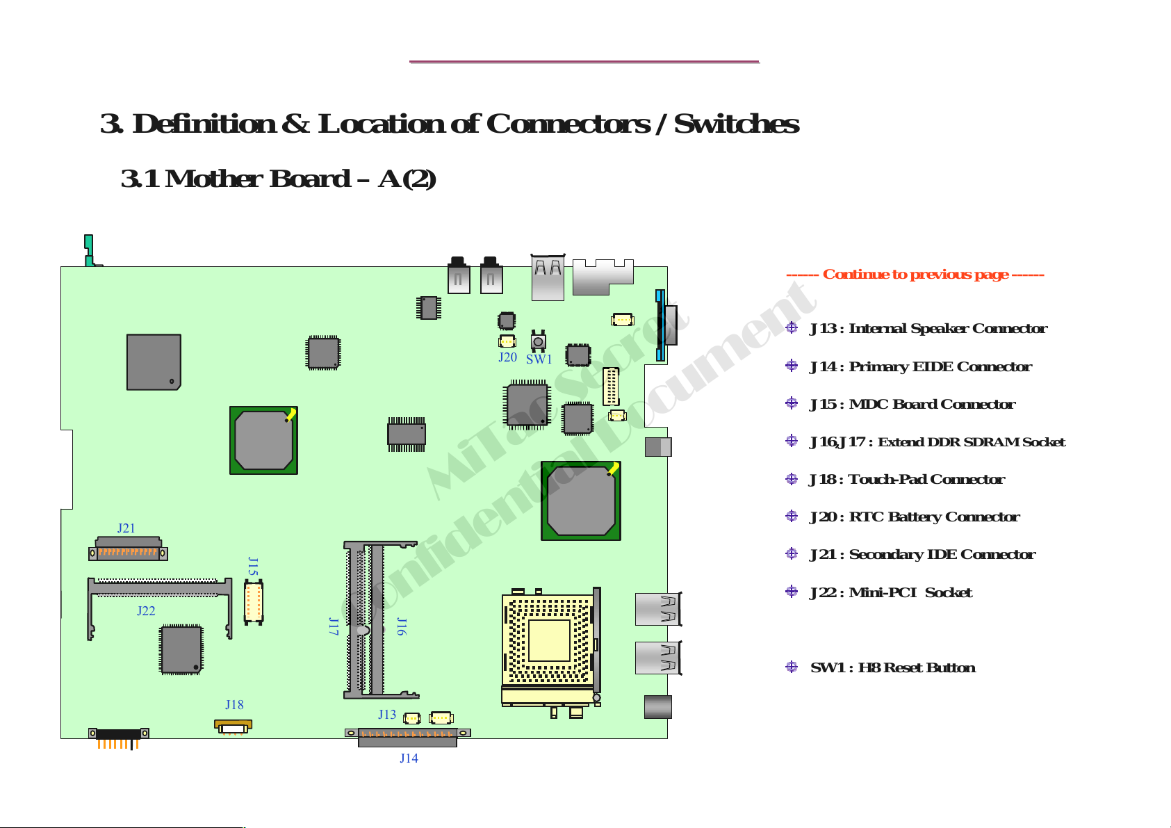
3. Definition & Location of Connectors / Switches
3.1 Mother Board – A(2)
J20
J509
SW1
------ Continue to previous page ------
J13 : Internal Speaker Connector
J14 : Primary EIDE Connector
J15 : MDC Board Connector
J16,J17 : Extend DDR SDRAM Socket
J21
J22
J18
J18 : Touch-Pad Connector
MiTac Secret
J20 : RTC Battery Connector
J15
J17
J16
J21 : Secondary IDE Connector
J22 : Mini-PCI Socket
Confidential Document
SW1 : H8 Reset Button
J13
J14
68
Page 70
8399
8399
N/B Maintenance
N/B Maintenance
3. Definition & Location of Connectors / Switches
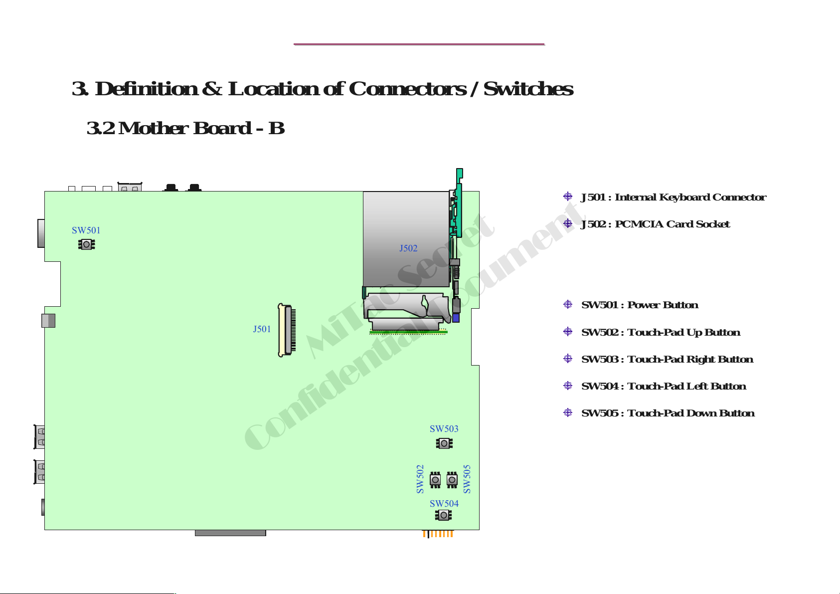
3.2 Mother Board - B
J501 : Internal Keybo ard Connect or
SW501
J502 : PCMCIA Card Socket
J502
J509
SW501 : Power Button
J501
MiTac Secret
SW503
SW502 : Touch-Pad Up Button
SW503 : Touch-Pad Right Button
SW504 : Touch-Pad Left Button
SW505 : Touch-Pad Down Button
Confidential Document
SW502
SW504
SW505
69
Page 71
8399
8399
N/B Maintenance
N/B Maintenance
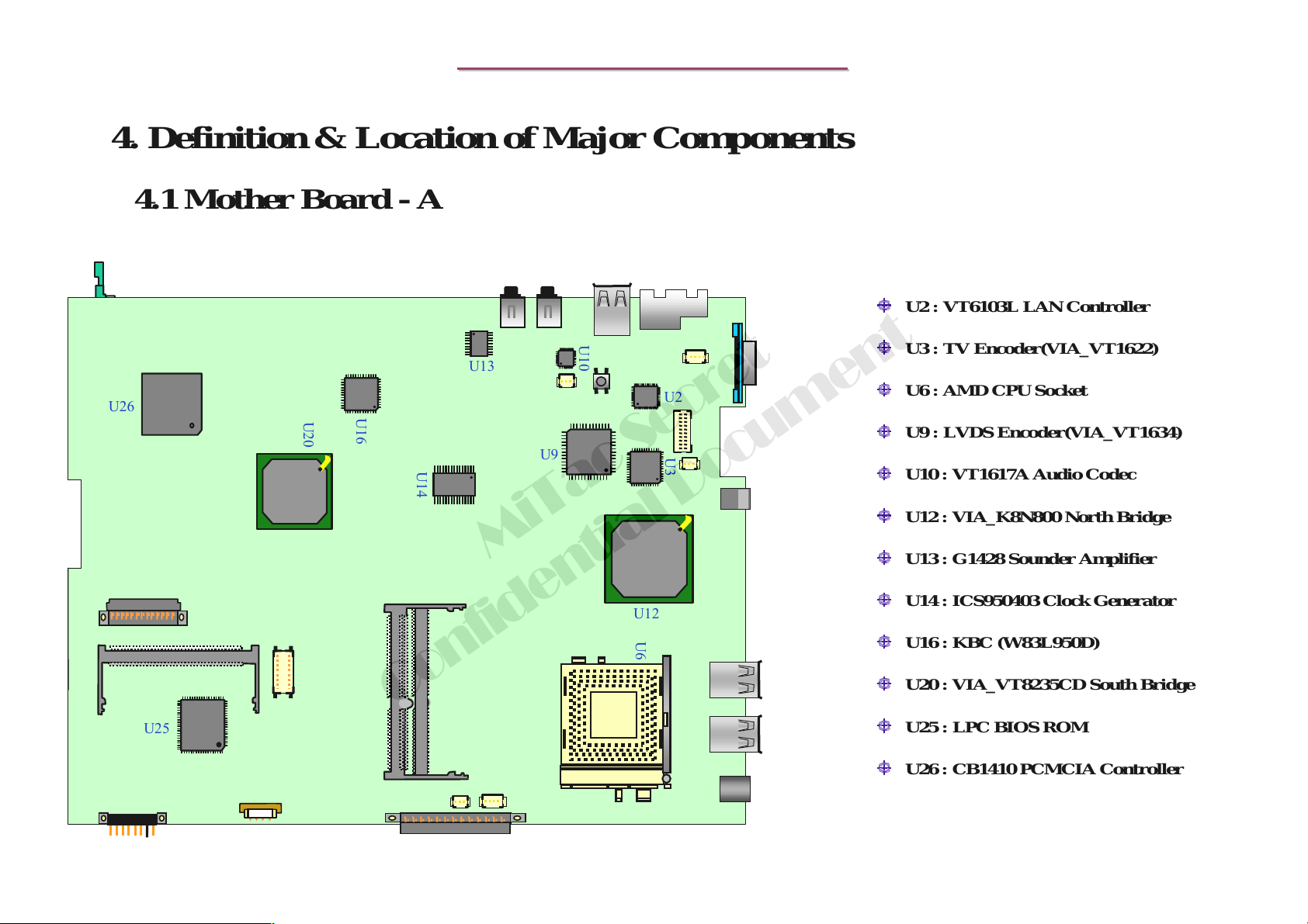
4. Definition & Location of Major Components
4.1 Mother Board - A
U2 : VT6103L LAN Controller
U26
U25
J509
U10
U13
U2
U20
U16
U14
U9
U3
MiTac Secret
U12
U6
U3 : TV Encoder(VIA_VT1622)
U6 : AMD CPU Socket
U9 : LVDS Encoder(VIA_VT1634)
U10 : VT1617A Audio Codec
U12 : VIA_K8N800 North Bridge
U13 : G1428 Sounder Am pli fi e r
U14 : ICS950403 Clock Generator
U16 : KBC (W83L950D)
U20 : VIA_VT8235CD South Bridge
Confidential Document
U25 : LPC BIOS ROM
U26 : CB1410 PCMCIA Controller
70
Page 72
8399
8399
N/B Maintenance
N/B Maintenance
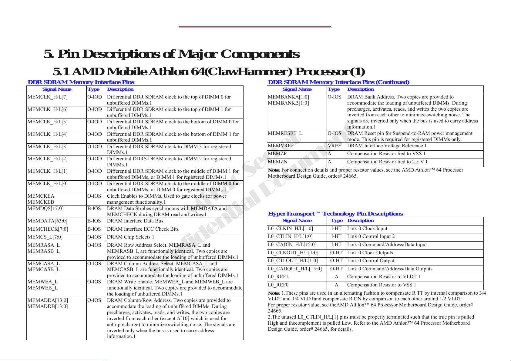
5. Pin Descriptions of Major Components
5.1 AMD Mobile Athlon 64(ClawHammer) Processor(1)
DDR SDRAM Memory Interface Pins
Signal Name Type Description
MEMCLK_H/L[7]
MEMCLK_H/L[6] O-IOD Differential DDR SDRAM clock to the top of DIMM 1 for
MEMCLK_H/L[5] O-IOD Differential DDR SDRAM clock to the bottom of DIMM 0 for
MEMCLK_H/L[4] O-IOD Differential DDR SDRAM clock to the bottom of DIMM 1 for
MEMCLK_H/L[3] O-IOD Differential DDR SDRAM clock to DIMM 3 for registered
MEMCLK_H/L[2] O-IOD Differential DDRS DRAM clock to DIMM 2 for registered
MEMCLK_H/L[1] O-IOD Differential DDR SDRAM clock to the middle of DIMM 1 for
MEMCLK_H/L[0] O-IOD Differential DDR SDRAM clock to the middle of DIMM 0 for
MEMCKEA
MEMCKEB
MEMDQS[17:0] B-IOS DRAM Data Strobes synchronous with MEMDATA and
MEMDATA[63:0] B-IOS DRAM Interface Data Bus
MEMCHECK[7:0] B-IOS DRAM Interface ECC Check Bits
MEMCS_L[7:0] O-IOS DRAM Chip Selects 1
MEMRASA_L
MEMRASB_L
MEMCASA_L
MEMCASB_L
MEMWEA_L
MEMWEB_L
MEMADDA[13:0]
MEMADDB[13:0]
O-IOD Differential DDR SDRAM clock to the top of DIMM 0 for
O-IOS Clock Enables to DIMMs. Used to gate clocks for power
O-IOS DRAM Row Address Select. MEMRASA_L and
O-IOS DRAM Column Address Select. MEMCASA_L and
O-IOS DRAM Write Enable. MEMWEA_L and MEMWEB_L are
O-IOS DRAM Column/Row Address. Two copies are provided to
unbuffered DIMMs.1
unbuffered DIMMs.1
unbuffered DIMMs.1
unbuffered DIMMs.1
DIMMs.1
DIMMs.1
unbuffered DIMMs, or DIMM 1 for registered DIMMs.1
unbuffered DIMMs, or DIMM 0 for registered DIMMs.1
management functionality.1
MEMCHECK during DRAM read and writes.1
MEMRASB_L are functionally identical. Two copies are
provided to accommodate the loading of unbuffered DIMMs.1
MEMCASB_L are functionally identical. Two copies are
provided to accommodate the loading of unbuffered DIMMs.1
functionally identical. Two copies are provided to accommodate
the loading of unbuffered DIMMs.1
accommodate the loading of unbuffered DIMMs. During
precharges, activates, reads, and writes, the two copies are
inverted from each other (except A[10] which is used for
auto-precharge) to minimize switching noise. The signals are
inverted only when the bus is used to carry address
information.1
Confidential Document
MiTac Secret
DDR SDRAM Memory Interface Pins (Continued)
Signal Name Type Descriptio n
MEMBANKA[1:0]
MEMBANKB[1:0]
MEMRESET_L O-IOS DRAM Reset pin for Suspend-to-RAM power management
MEMVREF VREF DRAM Interface Voltage Reference 1
MEMZP A Compensation Resistor tied to VSS 1
MEMZN A Compensation Resistor tied to 2.5 V 1
Note: For connection details and proper resistor values, see the AMD Athlon™ 64 Processor
Motherboard Design Guide, order# 24665.
O-IOS DRAM Bank Address. Two copies are provided to
accommodate the loading of unbuffered DIMMs. During
precharges, activates, reads, and writes the two copies are
inverted from each other to minimize switching noise. The
signals are inverted only when the bus is used to carry address
information.1
mode. This pin is required for registered DIMMs only.
HyperTransport™ Technology Pin Descriptions
Signal Name Type Description
L0_CLKIN_H/L[1:0] I-HT Link 0 Clock Input
L0_CTLIN_H/L[1:0] I-HT Link 0 Control Input 2
L0_CADIN_H/L[15:0] I-HT Link 0 Command/Address/Data Input
L0_CLKOUT_H/L[1:0] O-HT Link 0 Clock Outputs
L0_CTLOUT_H/L[1:0] O-HT Link 0 Control Output
L0_CADOUT_H/L[15:0] O-HT Link 0 Command/Address/Data Outputs
L0_REF1 A Compensation Resistor to VLDT 1
L0_REF0 A Compensation Resistor to VSS 1
Note: 1.These pins are used in an alternating fashion to compensate R TT by internal comparison to 3/4
VLDT and 1/4 VLDTand compensate R ON by comparison to each other around 1/2 VLDT.
For proper resistor value, see theAMD Athlon™ 64 Processor Motherboard Design Guide, order#
24665.
2.The unused L0_CTLIN_H/L[1] pins must be properly terminated such that the true pin is pulled
High and thecomplement is pulled Low. Refer to the AMD Athlon™ 64 Processor Motherboard
Design Guide, order# 24665, for details.
71
Page 73
8399
8399
N/B Maintenance
N/B Maintenance
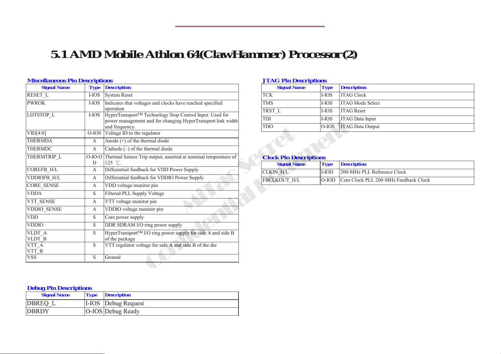
5.1 AMD Mobile Athlon 64(ClawHammer) Processor(2)
Miscellaneous Pin Descriptions
Signal Name Type Description
RESET_L I-IOS System Reset
PWROK I-IOS Indicates that voltages and clocks have reached specified
LDTSTOP_L I-IOS HyperTransport™ Technology Stop Control Input. Used for
VID[4:0] O-IOS Voltage ID to the regulator
THERMDA A Anode (+) of the thermal diode
THERMDC A Cathode (–) of the thermal diode
THERMTRIP_L O-IO-OD Thermal Sensor Trip output, asserted at nominal temperature of
COREFB_H/L A Differential feedback for VDD Power Supply
VDDIOFB_H/L A Differential feedback for VDDIO Power Supply
CORE_SENSE A VDD voltage monitor pin
VDDA S Filtered PLL Supply Voltage
VTT_SENSE A VTT voltage monitor pin
VDDIO_SENSE A VDDIO voltage monitor pin
VDD S Core power supply
VDDIO S DDR SDRAM I/O ring power supply
VLDT_A
VLDT_B
VTT_A
VTT_B
VSS S Ground
operation
power management and for changing HyperTransport link width
and frequency.
125 ℃.
MiTac Secret
S HyperTransport™ I/O ring power supply for side A and side B
of the package
S VTT regulator voltage for side A and side B of the die
JTAG Pin Descriptions
Signal Name Type Description
TCK I-IOS JTAG Clock
TMS I-IOS JTAG Mode Select
TRST_L I-IOS JTAG Reset
TDI I-IOS JTAG Data Input
TDO O-IOS JTAG Data Output
Clock Pin Descriptions
Signal Name Type Description
CLKIN_H/L I-IOD 200-MHz PLL Reference Clock
FBCLKOUT_H/L O-IOD Core Clock PLL 200-MHz Feedback Clock
Debug Pin Descri pt ions
Signal Name Type Description
DBREQ_L
DBRDY
I-IOS Debug Request
O-IOS Debug Ready
Confidential Document
72
Page 74
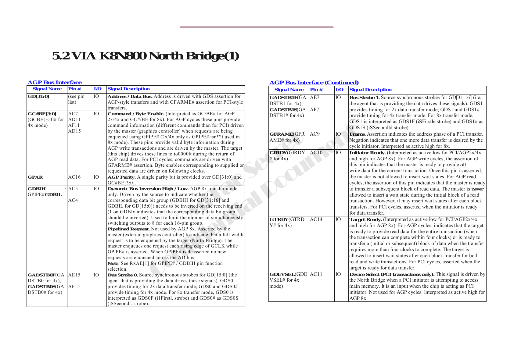
8399
8399
N/B Maintenance
N/B Maintenance
5.2 VIA K8N800 North Bridge(1)
AGP Bus Interface
Signal Name Pin # I/O Signal Description
GD[31:0]
GC#BE[3:0]
(GCBE[3:0]# for
4x mode)
GPAR
GDBIH /
GPIPE#GDBIL
GADSTB0F(GA
DSTB0 for 4x),
GADSTB0S(GA
DSTB0# for 4x)
(see pin
list)
AC7
AD11
AF11
AD15
AC16 IO AGP Parity. A single parity bit is provided over GD[31:0] and
AC5
AC4
AE15
AF15
IO Address / Data Bus. Address is driven with GDS assertion for
AGP-style transfers and with GFARME# assertion for PCI-style
transfers.
IO Command / B y te En ab le . (Interpreted as GC/BE# for AGP
2x/4x and GC#/BE for 8x). For AGP cycles these pins provide
command information (different commands than for PCI) driven
by the master (graphics controller) when requests are being
enqueued using GPIPE# (2x/4x only as GPIPE# isn™t used in
8x mode). These pins provide valid byte information during
AGP write transactions and are driven by the master. The target
(this chip) drives these lines to io0000lt during the return of
AGP read data. For PCI cycles, commands are driven with
GFARME# assertion. Byte enables corresponding to supplied or
requested data are driven on following clocks.
GC#BE[3:0].
IO Dynamic Bus Inversion H ig h / Low. AGP 8x transfer mode
only. Driven by the source to indicate whether the
corresponding data bit group (GDBIH for GD[31:16] and
GDBIL for GD[15:0]) needs to be inverted on the receiving end
(1 on GDBIx indicates that the corresponding data bit group
should be inverted). Used to limit the number of simultaneously
switching outputs to 8 for each 16-pin group.
Pipelined Request. Not used by AGP 8x. Asserted by the
master (external graphics controller) to indicate that a full-width
request is to be enqueued by the target (North Bridge). The
master enqueues one request each rising edge of GCLK while
GPIPE# is asserted. When GPIPE# is deasserted no new
requests are enqueued across the AD bus.
Note: See RxAE[1] for GPIPE# / GDBIH pin function
selection.
IO Bus Strobe 0. Source synchronous strobes for GD[15:0] (the
agent that is providing the data drives these signals). GDS0
provides timing for 2x data transfer mode; GDS0 and GDS0#
provide timing for 4x mode. For 8x transfer mode, GDS0 is
interpreted as GDS0F (i1Firstl. strobe) and GDS0# as GDS0S
(iSSecondl. strobe).
AGP Bus Interface (Continued)
Signal Name Pin # I/O Signal Description
GADSTB1F(GA
DSTB1 for 4x),
GADSTB1S(GA
DSTB1# for 4x)
GFRAME(GFR
AME# for 4x)
GIRDY(GIRDY
# for 4x)
MiTac Secret
Confidential Document
GTRDY(GTRD
Y# for 4x)
GDEVSEL(GDE
VSEL# for 4x
mode)
AE7
AF7
AC9 IO Frame. Assertion indicates the address phase of a PCI transfer.
AC10 IO Initiator Ready. (Interpreted as active low for PCI/AGP2x/4x
AC14 IO Target Ready. (Interpreted as active low for PCI/AGP2x/4x
AC11 IO Device Select (PCI transactions only). This signal is driven by
IO Bus Strobe 1. Source synchronous strobes for GD[31:16] (i.e.,
the agent that is providing the data drives these signals). GDS1
provides timing for 2x data transfer mode; GDS1 and GDS1#
provide timing for 4x transfer mode. For 8x transfer mode,
GDS1 is interpreted as GDS1F (iSFirstle strobe) and GDS1# as
GDS1S (iSSecondld strobe).
Negation indicates that one more data transfer is desired by the
cycle initiator. Interpreted as active high for 8x.
and high for AGP 8x). For AGP write cycles, the assertion of
this pin indicates that the master is ready to provide all
write data for the current transaction. Once this pin is asserted,
the master is not allowed to insert wait states. For AGP read
cycles, the assertion of this pin indicates that the master is ready
to transfer a subsequent block of read data. The master is never
allowed to insert a wait state during the initial block of a read
transaction. However, it may insert wait states after each block
transfers. For PCI cycles, asserted when the initiator is ready
for data transfer.
and high for AGP 8x). For AGP cycles, indicates that the target
is ready to provide read data for the entire transaction (when
the transaction can complete within four clocks) or is ready to
transfer a (initial or subsequent) block of data when the transfer
requires more than four clocks to complete. The target is
allowed to insert wait states after each block transfer for both
read and write transactions. For PCI cycles, asserted when the
target is ready for data transfer.
the North Bridge when a PCI initiator is attempting to access
main memory. It is an input when the chip is acting as PCI
initiator. Not used for AGP cycles. Interpreted as active high for
AGP 8x.
73
Page 75
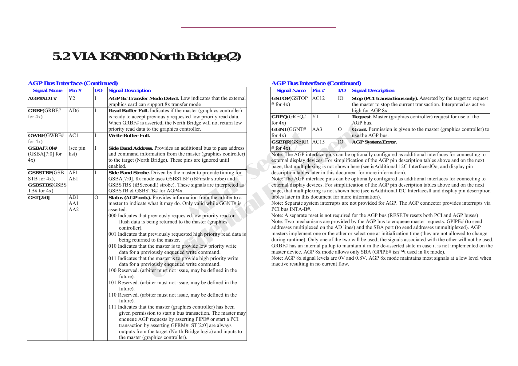
8399
b
8399
N/B Maintenance
N/B Maintenance
5.2 VIA K8N800 North Bridge(2)
AGP Bus Interface (Continued)
Signal Name Pin # I/O Signal Description
AGP8XDT#
GRBF(GRBF#
for 4x)
GWBF(GWBF#
for 4x)
GSBA[7:0]#
(GSBA[7:0] for
4x)
GSBSTBF
STB for 4x),
GSBSTBS
TB# for 4x)
GST[2:0]
Y2 I AGP 8x Transfer Mode Detect. Low indicates that the external
AD6 I Read Buffer Full. Indicates if the master (graphics controller)
AC1 I
(see pin
list)
(GSB
AF1
AE1
(GSBS
AB1
AA1
AA2
graphics card can support 8x transfer mode
is ready to accept previously requested low priority read data.
When GRBF# is asserted, the North Bridge will not return low
priority read data to the graphics controller.
Write Buffer Full.
I Side Band Address. Provides an additional bus to pass address
and command information from the master (graphics controller)
to the target (North Bridge). These pins are ignored until
enabled.
Side Band Strobe.
I
GSBA[7:0]. 8x mode uses GSBSTBF (iBFirstlr strobe) and
GSBSTBS (iBSecondl) strobe). These signals are interpreted as
GSBSTB & GSBSTB# for AGP4x.
O Status (AGP only). Provides information from the arbiter to a
master to indicate what it may do. Only valid while GGNT# is
asserted.
000 Indicates that previously requested low priority read or
flush data is being returned to the master (graphics
controller).
001 Indicates that previously requested high priority read data is
being returned to the master.
010 Indicates that the master is to provide low priority write
data for a previously enqueued write command.
011 Indicates that the master is to provide high priority write
data for a previously enqueued write command.
100 Reserved. (arbiter must not issue, may be defined in the
future).
101 Reserved. (arbiter must not issue, may be defined in the
future).
110 Reserved. (arbiter must not issue, may be defined in the
future).
111 Indicates that the master (graphics controller) has been
given permission to start a
enqueue AGP requests by asserting PIPE# or start a PCI
transaction by asserting GFRM#. ST[2:0] are always
outputs from the target (North Bridge logic) and inputs to
the master (graphics controller).
AGP Bus Interface (Continued)
Signal Name Pin # I/O Signal Description
Driven by the master to provide timing for
MiTac Secret
GSTOP(GSTOP
# for 4x)
GREQ(GREQ#
for 4x)
GGNT(GGNT#
for 4x)
GSERR(GSERR
# for 4x)
Note: The AGP interface pins can be optionally configured as additional interfaces for connecting to
external display devices. For simplification of the AGP pin description tables above and on the next
page, that multiplexing is not shown here (see isAdditional 12C InterfaceslÓo, and display pin
description tables later in this document for more information).
Note: The AGP interface pins can be optionally configured as additional interfaces for connecting to
external display devices. For simplification of the AGP pin description tables above and on the next
page, that multiplexing is not shown here (see isAdditional I2C Interfacesll and display pin description
tables later in this document for more information).
Note: Separate system interrupts are not provided for AGP. The AGP connector provides interrupts via
PCI bus INTA-B#.
Note: A separate reset is not required for the AGP bus (RESET# resets both PCI and AGP buses)
Note: Two mechanisms are provided by the AGP bus to enqueue master requests: GPIPE# (to send
addresses multiplexed on the AD lines) and the SBA port (to send addresses unmultiplexed). AGP
masters implement one or the other or select one at initialization time (they are not allowed to change
during runtime). Only one of the two will be used; the signals associated with the other will not be used.
GRBF# has an internal pullup to maintain it in the de-asserted state in case it is not implemented on the
master device. AGP 8x mode allows only SBA (GPIPE# isn™t used in 8x mode).
Note: AGP 8x signal levels are 0V and 0.8V. AGP 8x mode maintains most signals at a low level when
inactive resulting in no current flow.
AC12 IO Stop (PCI transactions only). Asserted by the target to request
Y1 I Request. Master (graphics controller) request for use of the
AA3 O Grant. Permission is given to the master (graphics controller) to
AC15 IO
the master to stop the current transaction. Interpreted as active
high for AGP 8x.
AGP bus.
use the AGP bus.
AGP System Error.
Confidential Document
us transaction. The master may
74
Page 76
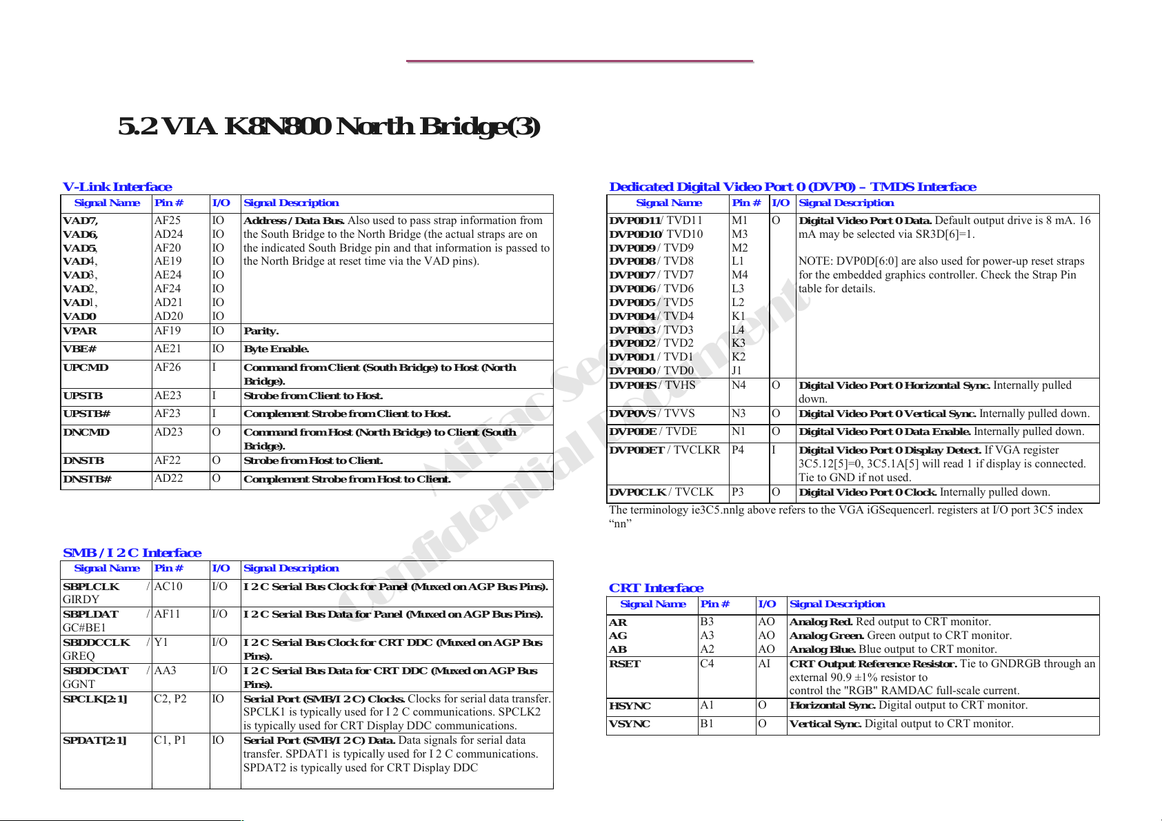
8399
8399
N/B Maintenance
N/B Maintenance
5.2 VIA K8N800 North Bridge(3)
V-Link Interface
Signal Name Pin # I/O Signal Description
VAD7,
VAD6,
VAD5,
VAD4,
VAD3,
VAD2,
VAD1,
VAD0
VPAR
VBE#
UPCMD
UPSTB
UPSTB#
DNCMD
DNSTB
DNSTB#
AF25
AD24
AF20
AE19
AE24
AF24
AD21
AD20
AF19 IO
AE21 IO
AF26 I
AE23 I
AF23 I
AD23 O
AF22 O
AD22 O
IO
Address / Data Bus. Also used to pass strap information from
IO
the South Bridge to the North Bridge (the actual straps are on
IO
the indicated South Bridge pin and that information is passed to
IO
the North Bridge at reset time via the VAD pins).
IO
IO
IO
IO
Parity.
Byte Enable.
Command from Client (South Bridge) to Host (North
Bridge).
Strobe from Client to Host.
Complement Strobe from Client to Host.
Command from Host (North Bridge) to Client (South
Bridge).
Strobe from Host to Client.
Complement Strobe from Host to Client.
SMB / I 2 C Interface
Signal Name Pin # I/O Signal Description
SBPLCLK /
GIRDY
SBPLDAT /
GC#BE1
SBDDCCLK /
GREQ
SBDDCDAT /
GGNT
SPCLK[2:1]
SPDAT[2:1]
AC10 I/O
AF11 I/O
Y1 I/O
AA3 I/O
C2, P2 IO Serial Port (SMB/I 2 C) Clocks. Clocks for serial data transfer.
C1, P1 IO Serial Port (SMB/I 2 C) Data. Data signals for serial data
I 2 C Serial Bus Clock for Panel (Muxed on AGP Bus Pins).
I 2 C Serial Bus Data for Panel (Muxed on AGP Bus Pins).
I 2 C Serial Bus Clock for CRT DDC (Muxed on AGP Bus
Pins).
I 2 C Serial Bus Data for CRT DDC (Muxed on AGP Bus
Pins).
SPCLK1 is typically used for I 2 C communications. SPCLK2
is typically used for CRT Display DDC communications.
transfer. SPDAT1 is typically used for I 2 C communications.
SPDAT2 is typically used for CRT Display DDC
communications.
Dedicated Digital Video Port 0 (DVP0) – TMDS Interface
Signal Name Pin # I/O Signal Description
O Digital Video Port 0 Data. Default output drive is 8 mA. 16
DVP0D11/ TVD11
DVP0D10/ TVD10
DVP0D9 / TVD9
DVP0D8 / TVD8
DVP0D7 / TVD7
DVP0D6 / TVD6
DVP0D5 / TVD5
DVP0D4 / TVD4
DVP0D3 / TVD3
DVP0D2 / TVD2
DVP0D1 / TVD1
DVP0D0 / TVD0
DVP0HS / TVHS N4 O Digital Video Port 0 Horizontal Sync. Internally pulled
DVP0VS / TVVS N3 O Digital Video Port 0 Vertical Sync. Internally pulled down.
DVP0DE / TVDE N1 O Digital Video Port 0 Data Enable. Internally pulled down.
DVP0DET / TVCLKR P4 I Digital Video Port 0 Display Detect. If VGA register
MiTac Secret
DVP0CLK / TVCLK P3 O Digital Video Port 0 Clock. Internally pulled down.
The terminology ie3C5.nnlg above refers to the VGA iGSequencerl. registers at I/O port 3C5 index
“nn”
M1
M3
M2
L1
M4
L3
L2
K1
L4
K3
K2
J1
mA may be selected via SR3D[6]=1.
NOTE: DVP0D[6:0] are also used for power-up reset straps
for the embedded graphics controller. Check the Strap Pin
table for details.
down.
3C5.12[5]=0, 3C5.1A[5] will read 1 if display is connected.
Tie to GND if not used.
CRT Interface
Signal Name Pin # I/O Signal Description
Confidential Document
AR
AG
AB
RSET
HSYNC
VSYNC
B3
A3
A2
C4 AI CRT Output Reference Resistor. Tie to GNDRGB through an
A1 O Horizontal Sync. Digital output to CRT monitor.
B1 O Vertical Sync. Digital output to CRT monitor.
AO
Analog Red. Red output to CRT monitor.
AO
Analog Green. Green output to CRT monitor.
AO
Analog Blue. Blue output to CRT monitor.
external 90.9 ±1% resistor to
control the "RGB" RAMDAC full-scale current.
75
Page 77
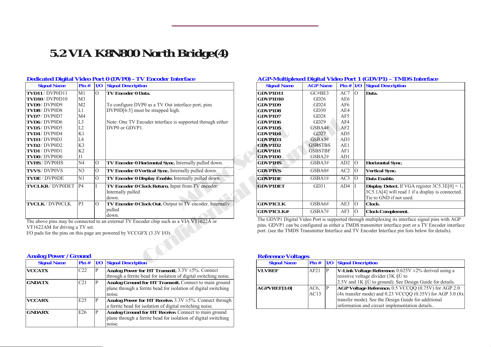
8399
8399
N/B Maintenance
N/B Maintenance
5.2 VIA K8N800 North Bridge(4)
Dedicated Digital Video Port 0 (DVP0) - TV Encoder Interface
Signal Name Pin # I/O Signal Description
TVD11 / DVP0D11
TVD10 / DVP0D10
TVD9 / DVP0D9
TVD8 / DVP0D8
TVD7 / DVP0D7
TVD6 / DVP0D6
TVD5 / DVP0D5
TVD4 / DVP0D4
TVD3 / DVP0D3
TVD2 / DVP0D2
TVD1 / DVP0D1
TVD0
/ DVP0D0
TVHS / DVP0HS N4 O TV Encoder 0 Horizonta l Sync. Internally pulled down.
TVVS / DVP0VS N3 O TV Encoder 0 Vertical Sync. Internally pulled down.
TVDE / DVP0DE N1 O TV Encoder 0 Display Enabl e. Internally pulled down.
TVCLKR / DVP0DET P4 I TV Encoder 0 Clock Return. Input from TV encoder.
TVCLK / DVP0CLK P3 O TV Encoder 0 Clock Out. Output to TV encoder. Internally
The above pins may be connected to an external TV Encoder chip such as a VIA VT1622A or
VT1622AM for driving a TV set.
I/O pads for the pins on this page are powered by VCCGFX (3.3V I/O).
M1
M3
M2
L1
M4
L3
L2
K1
L4
K3
K2
J1
O
TV Encoder 0 Data.
To configure DVP0 as a TV Out interface port, pins
DVP0D[6:5] must be strapped high.
Note: One TV Encoder interface is supported through either
DVP0 or GDVP1.
Internally pulled
down.
pulled
down.
MiTac Secret
AGP-Multiplexed Digital Video Port 1 (GDVP1) – TMDS Interface
Signal Name AGP Name Pin # I/O Signal Description
GDVP1D11
GDVP1D10
GDVP1D9
GDVP1D8
GDVP1D7
GDVP1D6
GDVP1D5
GDVP1D4
GDVP1D3
GDVP1D2
GDVP1D1
GDVP1D0
GDVP1HS
GDVP1VS
GDVP1DE
GDVP1DET
GDVP1CLK
GDVP1CLK#
The GDVP1 Digital Video Port is supported through multiplexing its interface signal pins with AGP
pins. GDVP1 can be configured as either a TMDS transmitter interface port or a TV Encoder interface
port. (see the TMDS Transmitter Interface and TV Encoder Interface pin lists below for details).
GC#BE3
GD26
GD24
GD30
GD28
GD29
GSBA4#
GD27
GSBA5#
GSBSTBS
GSBSTBF
GSBA2#
GSBA3# AD2 O
GSBA0# AC2 O
GSBA1# AC3 O
GD31 AD4 I Display Detect. If VGA register 3C5.3E[0] = 1,
GSBA6# AE3 O
GSBA7# AF3 O
AC7
AE6
AF6
AE4
AF5
AF4
AF2
AD5
AD3
AE1
AF1
AD1
O
Data.
Horizontal Sync.
Vertical Sync.
Data Enable.
3C5.1A[4] will read 1 if a display is connected.
Tie to GND if not used.
Clock.
Clock Complement.
Analog Power / Ground
Signal Name Pin # I/O Signal Descrip tion
VCCATX
GNDATX
VCCARX
GNDARX
C22 P
C21 P
E25 P
E26 P
Analog Po wer for HT Transmit.
through a ferrite bead for isolation of digital switching noise.
Analog Ground for HT Transmit.
plane through a ferrite bead for isolation of digital switching
noise.
Analog Power for HT Receive.
a ferrite bead for isolation of digital switching noise.
Analog Ground for HT Receive.
plane through a ferrite bead for isolation of digital switching
noise.
Reference Voltages
Confidential Document
3.3V ±5%. Connect
Connect to main ground
3.3V ±5%. Connect through
Connect to main ground
Signal Name Pin # I/O Signal Description
VLVREF
AGPVREF[1:0]
AF21 P V-Link Voltage Reference. 0.625V ±2% derived using a
AC6,
AC13
resistive voltage divider (3K §Ù to
2.5V and 1K §Ù to ground). See Design Guide for details.
P AGP Voltage Reference. 0.5 VCCQQ (0.75V) for AGP 2.0
(4x transfer mode) and 0.23 VCCQQ (0.35V) for AGP 3.0 (8x
transfer mode). See the Design Guide for additional
information and circuit implementation details..
76
Page 78
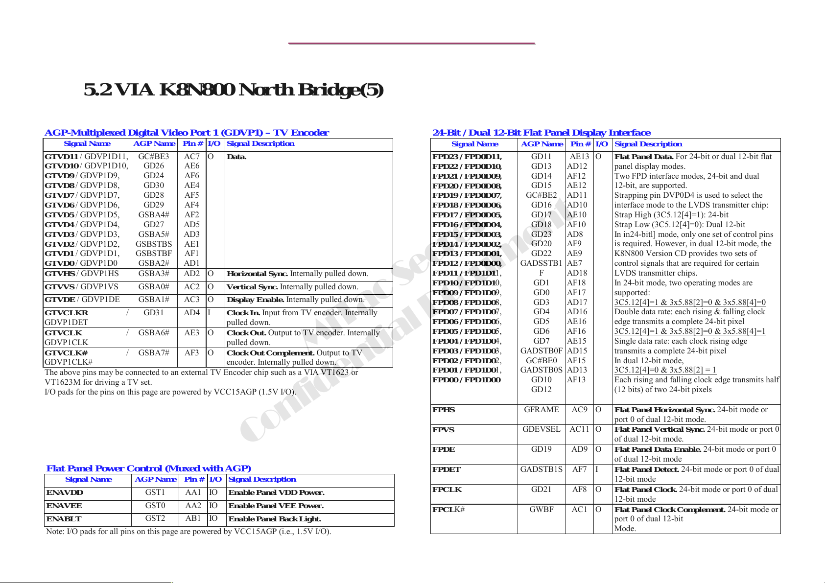
8399
b
b
8399
N/B Maintenance
N/B Maintenance
5.2 VIA K8N800 North Bridge(5)
AGP-Multiplexed Digital Video Port 1 (GDVP1) – TV Encoder
Signal Name AGP Name Pin # I/O Signal Description
GTVD11 / GDVP1D11,
GTVD10 / GDVP1D10,
GTVD9 / GDVP1D9,
GTVD8 / GDVP1D8,
GTVD7 / GDVP1D7,
GTVD6
GTVD5 / GDVP1D5,
GTVD4 / GDVP1D4,
GTVD3 / GDVP1D3,
GTVD2 / GDVP1D2,
GTVD1 / GDVP1D1,
GTVD0 / GDVP1D0
GTVHS / GDVP1HS GSBA3# AD2 O Horizontal Sync. Internally pulled down.
GTVVS / GDVP1VS GSBA0# AC2 O Vertical Sync. Internally pulled down.
GTVDE / GDVP1DE GSBA1# AC3 O Display Enable. Internally pulled down.
GTVCLKR /
GDVP1DET
GTVCLK /
GDVP1CLK
GTVCLK# /
GDVP1CLK#
The above pins may be connected to an external TV Encoder chip such as a VIA VT1623 or
VT1623M for driving a TV set.
I/O pads for the pins on this page are powered by VCC15AGP (1.5V I/O).
/ GDVP1D6,
GC#BE3
GD26
GD24
GD30
GD28
GD29
GSBA4#
GD27
GSBA5#
GSBSTBS
GSBSTBF
GSBA2#
GD31 AD4 I Clock In. Input from TV encoder. Internally
GSBA6# AE3 O Clock Out. Output to TV encoder. Internally
GSBA7# AF3 O Clock Out Complement. Output to TV
AC7
AE6
AF6
AE4
AF5
AF4
AF2
AD5
AD3
AE1
AF1
AD1
O
Data.
pulled down.
pulled down.
encoder. Internally pulled down.
MiTac Secret
Confidential Document
Flat Panel Power Control (Muxed with AGP)
Signal Name AGP Name Pin # I/O Signal Description
ENAVDD
ENAVEE
ENABLT
Note: I/O pads for all pins on this page are powered by VCC15AGP (i.e., 1.5V I/O).
GST1 AA1 IO
GST0 AA2 IO
GST2 AB1 IO
Enable Panel VDD Power.
Enable Panel VEE Power.
Enable Panel Back Light.
24-Bit / Dual 12-Bit Flat Panel Display Interface
Signal Name AGP Name Pin # I/O Signal Description
FPD23 / FPD0D11,
FPD22 / FPD0D10,
FPD21 / FPD0D09,
FPD20 / FPD0D08,
FPD19 / FPD0D07,
FPD18 / FPD0D06,
FPD17 / FPD0D05,
FPD16 / FPD0D04,
FPD15 / FPD0D03,
FPD14 / FPD0D02,
FPD13 / FPD0D01,
FPD12 / FPD0D00,
FPD11 / FPD1D11,
FPD10 / FPD1D10,
FPD09 / FPD1D09,
FPD08 / FPD1D08,
FPD07 / FPD1D07,
FPD06 / FPD1D06,
FPD05 / FPD1D05,
FPD04 / FPD1D04,
FPD03 / FPD1D03,
FPD02 / FPD1D02,
FPD01 / FPD1D01,
FPD00 / FPD1D00
FPHS
FPVS
FPDE
FPDET
FPCLK
FPCLK# GWBF AC1 O Flat Panel Clock Complement. 24-bit mode or
GD11
GD13
GD14
GD15
GC#BE2
GD16
GD17
GD18
GD23
GD20
GD22
GADSSTB1
F
GD1
GD0
GD3
GD4
GD5
GD6
GD7
GADSTB0F
GC#BE0
GADSTB0S
GD10
GD12
GFRAME AC9 O Flat Panel Horizontal Sync. 24-bit mode or
GDEVSEL AC11 O Flat Panel Vertical Sync. 24-
GD19 AD9 O Flat Panel Data Enable. 24-bit mode or port 0
GADSTB1S AF7 I Flat Panel Detect. 24-
GD21 AF8 O Flat Panel Clock. 24-bit mode or port 0 of dual
AE13
O Flat Panel Data. For 24-bit or dual 12-bit flat
AD12
AF12
AE12
AD11
AD10
AE10
AF10
AD8
AF9
AE9
AE7
AD18
AF18
AF17
AD17
AD16
AE16
AF16
AE15
AD15
AF15
AD13
AF13
panel display modes.
Two FPD interface modes, 24-bit and dual
12-bit, are supported.
Strapping pin DVP0D4 is used to select the
interface mode to the LVDS transmitter chip:
Strap High (3C5.12[4]=1): 24-bit
Strap Low (3C5.12[4]=0): Dual 12-bit
In in24-bitl] mode, only one set of control pins
is required. However, in dual 12-bit mode, the
K8N800 Version CD provides two sets of
control signals that are required for certain
LVDS transmitter chips.
In 24-bit mode, two operating modes are
supported:
3C5.12[4]=1 & 3x5.88[2]=0 & 3x5.88[4]=0
Double data rate: each rising & falling clock
edge transmits a complete 24-bit pixel
3C5.12[4]=1 & 3x5.88[2]=0 & 3x5.88[4]=1
Single data rate: each clock rising edge
transmits a complete 24-bit pixel
In dual 12-bit mode,
3C5.12[4]=0 & 3x5.88[2] = 1
Each rising and falling clock edge transmits half
(12 bits) of two 24-bit pixels
port 0 of dual 12-bit mode.
of dual 12-bit mode.
of dual 12-bit mode
it mode or port 0 of dual
12-bit mode
12-bit mode
port 0 of dual 12-bit
Mode.
it mode or port 0
77
Page 79
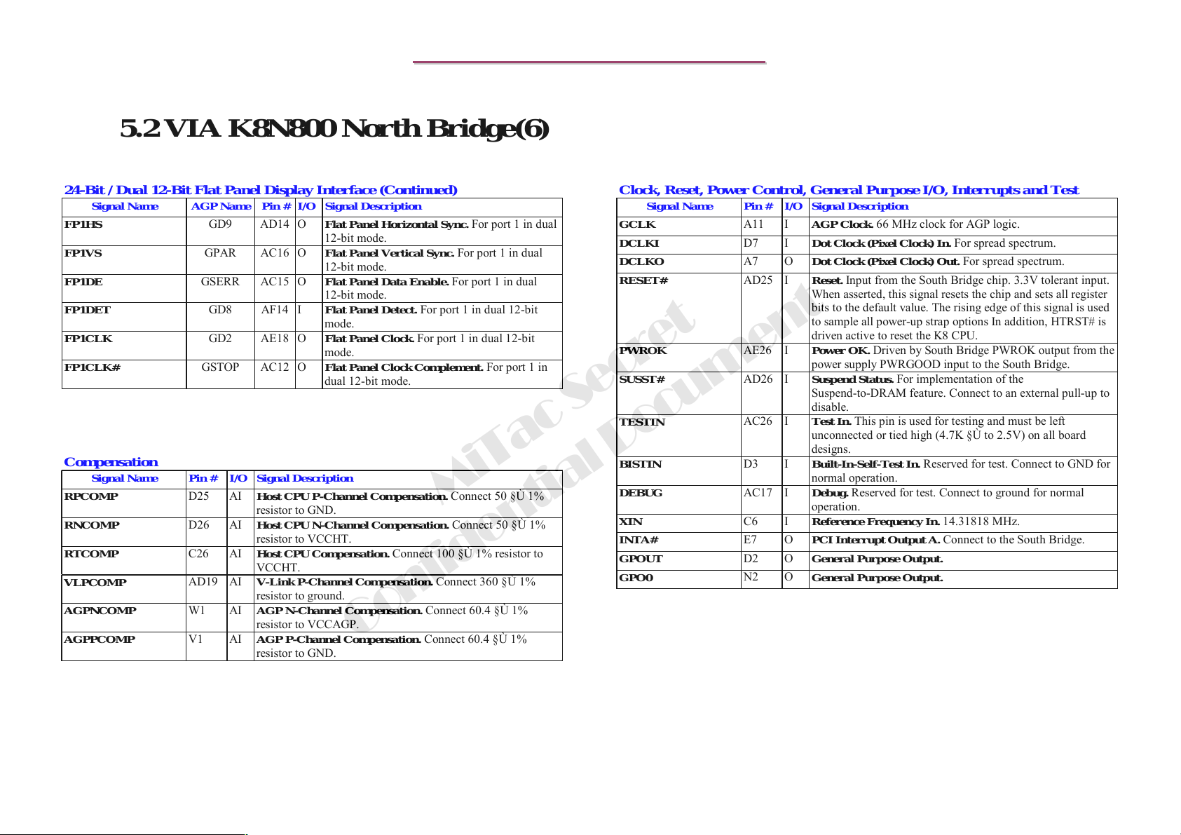
8399
8399
N/B Maintenance
N/B Maintenance
5.2 VIA K8N800 North Bridge(6)
24-Bit / Dual 12-Bit Flat Panel Display Interface (Continued)
Signal Name AGP Name Pin # I/O Signal Descriptio n
FP1HS
FP1VS
FP1DE
FP1DET
FP1CLK
FP1CLK#
GD9 AD14 O Flat Panel Horizontal Sync. For port 1 in dual
GPAR AC16 O
GSERR AC15 O Flat Panel Data Enable. For port 1 in dual
GD8 AF14 I Flat Panel Detect. For port 1 in dual 12-bit
GD2 AE18 O Flat Panel Clock. For port 1 in dual 12-bit
GSTOP AC12 O Flat Panel Clock Complement. For port 1 in
12-bit mode.
Flat Panel Vertical Sync.
12-bit mode.
12-bit mode.
mode.
mode.
dual 12-bit mode.
Compensation
Signal Name Pin # I/O Signal Description
RPCOMP
RNCOMP
RTCOMP
VLPCOMP
AGPNCOMP
AGPPCOMP
D25 AI Host CPU P-Channel Compensation. Connect 50 §Ù 1%
D26 AI Host CPU N-Channel Compensation. Connect 50 §Ù 1%
C26 AI Host CPU Compensation. Connect 100 §Ù 1% resistor to
AD19 AI V-Link P-Channel Compensation. Connect 360 §Ù 1%
W1 AI AGP N-Channel Compensation. Connect 60.4 §Ù 1%
V1 AI AGP P-Channel Compensation. Connect 60.4 §Ù 1%
resistor to GND.
resistor to VCCHT.
VCCHT.
resistor to ground.
resistor to VCCAGP.
resistor to GND.
Confidential Document
MiTac Secret
For port 1 in dual
Clock, Reset, Power Control, General Purpose I/O, Interrupts and Test
Signal Name Pin # I/O Signal Description
GCLK
DCLKI
DCLKO
RESET#
PWROK
SUSST#
TESTIN
BISTIN
DEBUG
XIN
INTA#
GPOUT
GPO0
A11 I AGP Clock. 66 MHz clock for AGP logic.
D7 I Dot Clock (Pi x e l Clock) In . For spread spectrum.
A7 O Dot Clock (Pixel Clock) Out. For spread spectrum.
AD25 I Reset. Input from the South Bridge chip. 3.3V tolerant input.
AE26 I Pow er OK. Driven by South Bridge PWROK output from the
AD26 I Suspend Status. For implementation of the
AC26 I Test In. This pin is used for testing and must be left
D3 I Built-In-Self-Test In. Reserved for test. Connect to GND for
AC17 I
C6 I Reference Frequency In. 14.31818 MHz.
E7 O PCI Interrupt Output A. Connect to the South Bridge.
D2 O
N2 O
When asserted, this signal resets the chip and sets all register
bits to the default value. The rising edge of this signal is used
to sample all power-up strap options In addition, HTRST# is
driven active to reset the K8 CPU.
power supply PWRGOOD input to the South Bridge.
Suspend-to-DRAM feature. Connect to an external pull-up to
disable.
unconnected or tied high (4.7K §Ù to 2.5V) on all board
designs.
normal operation.
Debug.
Reserved for test. Connect to ground for normal
operation.
General Purpose Output.
General Purpose Output.
78
Page 80
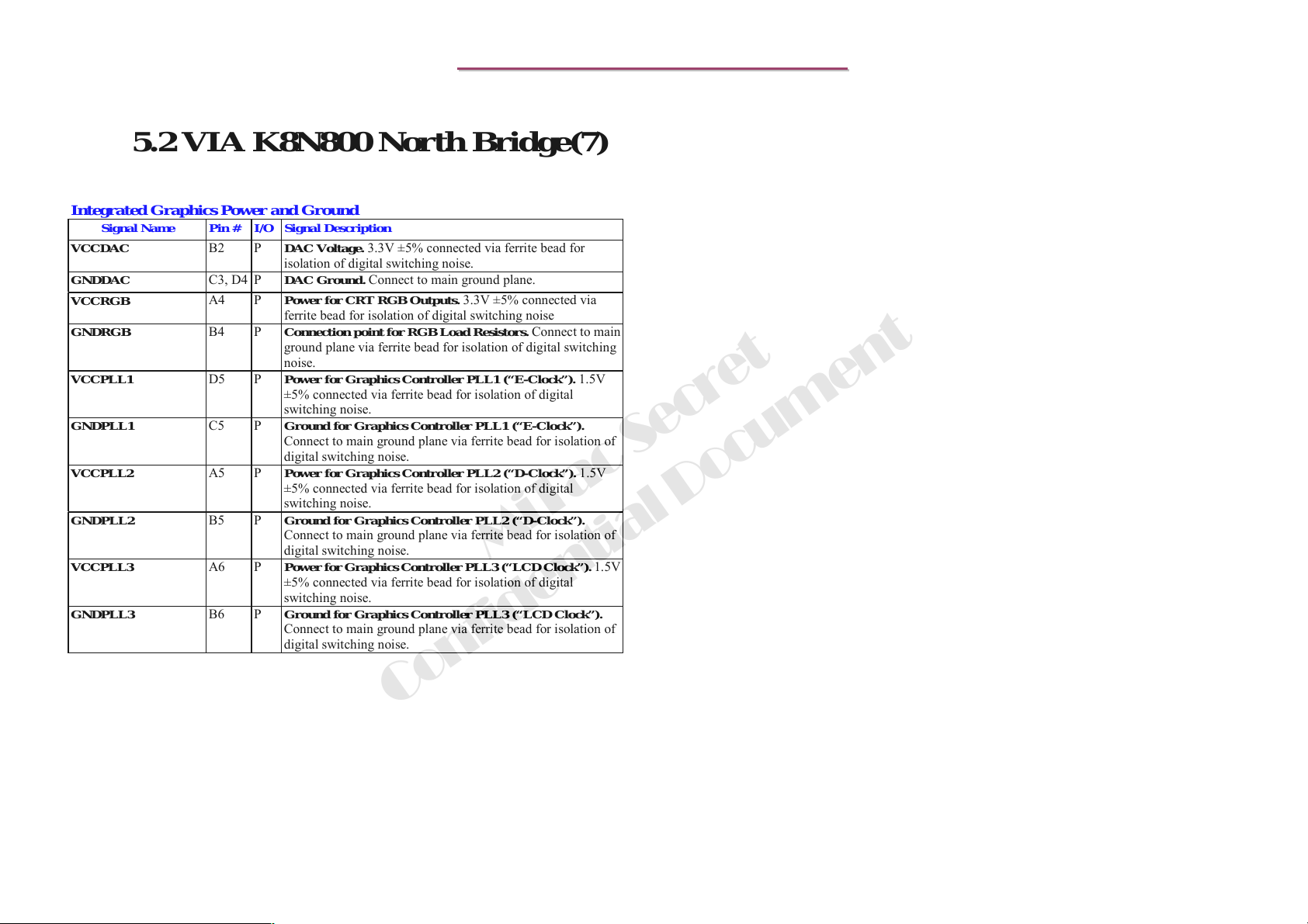
5.2 VIA K8N800 North Bridge(7)
Integrated Graphics Power and Ground
Signal Name Pin # I/O Signal Description
VCCDAC
GNDDAC
VCCRGB
GNDRGB
VCCPLL1
GNDPLL1
VCCPLL2
GNDPLL2
VCCPLL3
GNDPLL3
B2 P DAC Voltage. 3.3V ±5% connected via ferrite bead for
C3, D4 P DAC Ground. Connect to main ground plane.
A4 P Power for CRT RGB Outputs. 3.3V ±5% connected via
B4 P
D5 P Power for Graphics Controller PLL1 (“E-Clock”). 1.5V
C5 P
A5 P Power for Graphics Controller PLL2 (“D-Clock”). 1.5V
B5 P
A6 P Power for Graphics Controller PLL3 (“LCD Clock”). 1.5V
B6 P
isolation of digital switching noise.
ferrite bead for isolation of digital switching noise
Connection point for RGB Load Resistors.
ground plane via ferrite bead for isolation of digital switching
noise.
±5% connected via ferrite bead for isolation of digital
switching noise.
Ground for Graphics Controller PLL1 (“E-Clock”).
Connect to main ground plane via ferrite bead for isolation of
digital switching noise.
±5% connected via ferrite bead for isolation of digital
switching noise.
Ground for Graphics Controller PLL2 (“D-Clock”).
Connect to main ground plane via ferrite bead for isolation of
digital switching noise.
±5% connected via ferrite bead for isolation of digital
switching noise.
Ground for Graphics Controller PLL3 (“L CD Clock”).
Connect to main ground plane via ferrite bead for isolation of
digital switching noise.
8399
8399
N/B Maintenance
N/B Maintenance
Connect to main
MiTac Secret
Confidential Document
79
Page 81
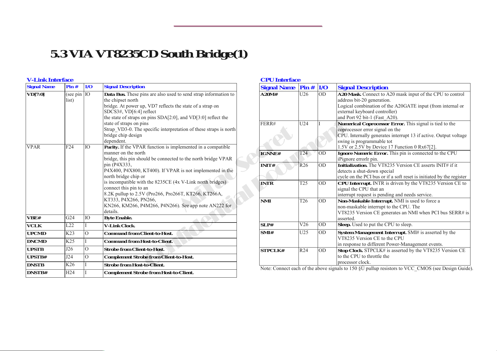
8399
8399
N/B Maintenance
N/B Maintenance
5.3 VIA VT8235CD South Bridge(1)
V-Link Interface
Signal Name Pin # I/O Signal Description
VD[7:0]
VPAR F24 IO Parity. If the VPAR function is implemented in a compatible
VBE#
VCLK
UPCMD
DNCMD
UPSTB
UPSTB#
DNSTB
DNSTB#
(see pin
list)
G24 IO
L22 I
K23 O
K25 I
J26 O
J24 O
K26 I
H24 I
IO Data Bus. These pins are also used to send strap information to
the chipset north
bridge. At power up, VD7 reflects the state of a strap on
SDCS3#, VD[6:4] reflect
the state of straps on pins SDA[2:0], and VD[3:0] reflect the
state of straps on pins
Strap_VD3-0. The specific interpretation of these straps is north
bridge chip design
dependent.
manner on the north
bridge, this pin should be connected to the north bridge VPAR
pin (P4X333,
P4X400, P4X800, KT400). If VPAR is not implemented in the
north bridge chip or
is incompatible with the 8235CE (4x V-Link north bridges)
connect this pin to an
8.2K pullup to 2.5V (Pro266, Pro266T, KT266, KT266A,
KT333, P4X266, PN266,
KN266, KM266, P4M266, P4N266). See app note AN222 for
details.
Byte Enable.
V-Link Clock.
Command from Client-to-Host.
Command from Host-to-Client.
Strobe from Client-to-Host.
Complement Strobe from Client-to-Host.
Strobe from Host-to-Client.
Complement Strobe from Host-to-Client.
Confidential Document
MiTac Secret
CPU Interface
Signal Name Pin # I/O Signal Description
A20M#
FERR# U24 I Numerical Coprocessor Error. This signal is tied to the
IGNNE#
INIT#
INTR
NMI
SLP#
SMI#
STPCLK#
Note: Connect each of the above signals to 150 §Ù pullup resistors to VCC_CMOS (see Design Guide).
U26 OD A20 Mask. Connect to A20 mask input of the CPU to control
T24 OD Ignore Numeric Error. This pin is connected to the CPU
R26 OD
T25 OD CPU Interrupt. INTR is driven by the VT8235 Version CE to
T26 OD Non-Maskable Interrupt. NMI is used to force a
V26 OD Sleep. Used to put the CPU to sleep.
U25 OD System Management Interrupt. SMI# is asserted by the
R24 OD Stop Clock. STPCLK# is asserted by the VT8235 Version CE
address bit-20 generation.
Logical combination of the A20GATE input (from internal or
external keyboard controller)
and Port 92 bit-1 (Fast_A20).
coprocessor error signal on the
CPU. Internally generates interrupt 13 if active. Output voltage
swing is programmable tot
1.5V or 2.5V by Device 17 Function 0 Rx67[2].
iPignore errorlr pin.
Initialization.
detects a shut-down special
cycle on the PCI bus or if a soft reset is initiated by the register
signal the CPU that an
interrupt request is pending and needs service.
non-maskable interrupt to the CPU. The
VT8235 Version CE generates an NMI when PCI bus SERR# is
asserted.
VT8235 Version CE to the CPU
in response to different Power-Management events.
to the CPU to throttle the
processor clock.
The VT8235 Version CE asserts INIT# if it
80
Page 82
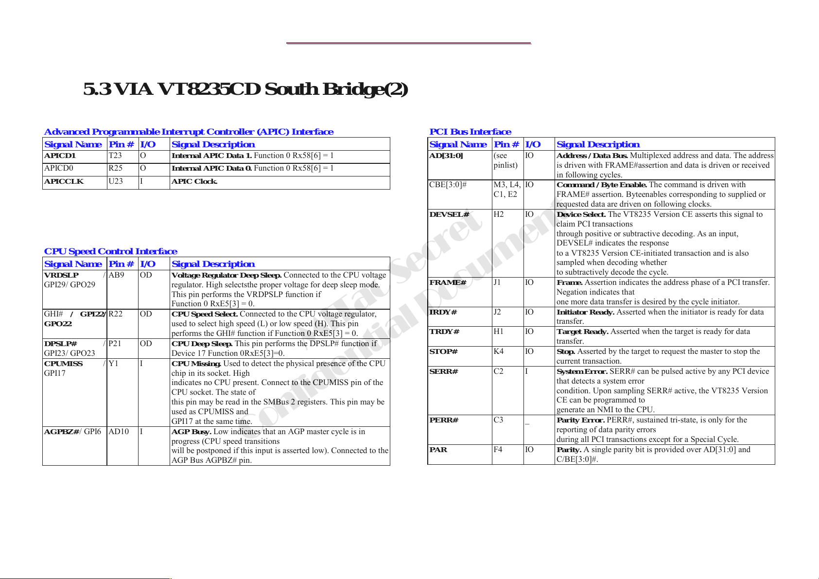
8399
8399
N/B Maintenance
N/B Maintenance
5.3 VIA VT8235CD South Bridge(2)
Advanced Programmable Interrupt Controller (APIC) Interface
Signal Name Pin # I/O Signal Description
APICD1
APICD0 R25 O Internal APIC Data 0. Function 0 Rx58[6] = 1
APICCLK
T23 O
U23 I
Internal APIC Data 1.
APIC Clock.
Function 0 Rx58[6] = 1
CPU Speed Control Interface
Signal Name Pin # I/O Signal Description
VRDSLP /
GPI29/ GPO29
GHI# / GPI22/
GPO22
DPSLP# /
GPI23/ GPO23
CPUMISS /
GPI17
AGPBZ# / GPI6 AD10 I AGP Busy. Low indicates that an AGP master cycle is in
AB9 OD Voltage Regulator Deep Sleep. Connected to the CPU voltage
R22 OD CPU Speed Sel ect. Connected to the CPU voltage regulator,
P21 OD CPU Deep Sleep. This pin performs the DPSLP# function if
Y1 I CPU M i ssing . Used to detect the physical presence of the CPU
regulator. High selectsthe proper voltage for deep sleep mode.
This pin performs the VRDPSLP function if
Function 0 RxE5[3] = 0.
used to select high speed (L) or low speed (H). This pin
performs the GHI# function if Function 0 RxE5[3] = 0.
Device 17 Function 0RxE5[3]=0.
chip in its socket. High
indicates no CPU present. Connect to the CPUMISS pin of the
CPU socket. The state of
this pin may be read in the SMBus 2 registers. This pin may be
used as CPUMISS and
GPI17 at the same time.
progress (CPU speed transitions
will be postponed if this input is asserted low). Connected to the
AGP Bus AGPBZ# pin.
Confidential Document
MiTac Secret
PCI Bus In t erface
Signal Name Pin # I/O Signal Description
AD[31:0]
CBE[3:0]# M3, L4,
DEVSEL#
FRAME#
IRDY#
TRDY#
STOP#
SERR#
PERR#
PAR
(see
pinlist)
C1, E2
H2 IO
J1 IO Frame. Assertion indicates the address phase of a PCI transfer.
J2 IO Initiator Ready. Asserted when the initiator is ready for data
H1 IO Target Ready. Asserted when the target is ready for data
K4 IO Stop. Asserted by the target to request the master to stop the
C2 I System Error. SERR# can be pulsed active by any PCI device
C3 _ Parity Error. PERR#, sustained tri-state, is only for the
F4 IO Parity. A single parity bit is provided over AD[31:0] and
IO Address / Data Bus. Multiplexed address and data. The address
IO Command / Byte Enable. The command is driven with
is driven with FRAME#assertion and data is driven or received
in following cycles.
FRAME# assertion. Byteenables corresponding to supplied or
requested data are driven on following clocks.
Device Select.
claim PCI transactions
through positive or subtractive decoding. As an input,
DEVSEL# indicates the response
to a VT8235 Version CE-initiated transaction and is also
sampled when decoding whether
to subtractively decode the cycle.
Negation indicates that
one more data transfer is desired by the cycle initiator.
transfer.
transfer.
current transaction.
that detects a system error
condition. Upon sampling SERR# active, the VT8235 Version
CE can be programmed to
generate an NMI to the CPU.
reporting of data parity errors
during all PCI transactions except for a Special Cycle.
C/BE[3:0]#.
The VT8235 Version CE asserts this signal to
81
Page 83
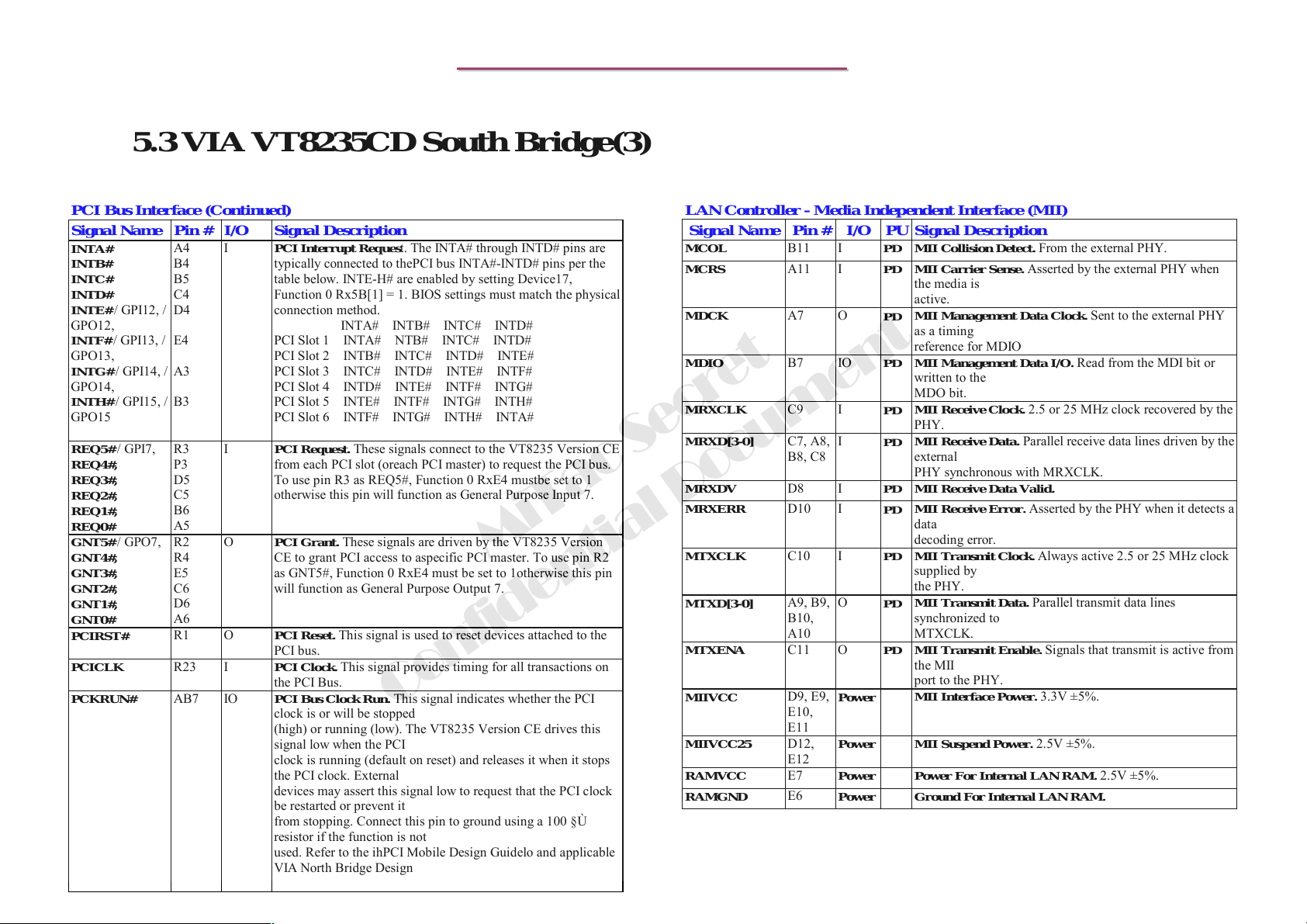
8399
8399
N/B Maintenance
N/B Maintenance
5.3 VIA VT8235CD South Bridge(3)
PCI Bus Interface (Continued)
Signal Name Pin # I/O Signal Description
INTA#
INTB#
INTC#
INTD#
INTE# / GPI12, /
GPO12,
INTF#
/ GPI13, /
GPO13,
INTG# / GPI14, /
GPO14,
INTH# / GPI15, /
GPO15
REQ5#
/ GPI7,
REQ4#,
REQ3#,
REQ2#,
REQ1#,
REQ0#
GNT5# / GPO7,
GNT4#,
GNT3#,
GNT2#,
GNT1#,
GNT0#
PCIRST#
PCICLK
PCKRUN#
A4
B4
B5
C4
D4
E4
A3
B3
R3
P3
D5
C5
B6
A5
R2
R4
E5
C6
D6
A6
R1 O PCI Reset. This signal is used to reset devices attached to the
R23 I PCI Clock. This signal provides timing for all transactions on
AB7 IO PCI Bus Clock Run. This signal indicates whether the PCI
I PCI Interrupt Request. The INTA# through INTD# pins are
I
O PCI Grant. These signals are driven by the VT8235 Version
typically connected to thePCI bus INTA#-INTD# pins per the
table below. INTE-H# are enabled by setting Device17,
Function 0 Rx5B[1] = 1. BIOS settings must match the physical
connection method.
PCI Slot 1 INTA# NTB# INTC# INTD#
PCI Slot 2 INTB# INTC# INTD# INTE#
PCI Slot 3 INTC# INTD# INTE# INTF#
PCI Slot 4 INTD# INTE# INTF# INTG#
PCI Slot 5 INTE# INTF# INTG# INTH#
PCI Slot 6 INTF# INTG# INTH# INTA#
PCI Request.
from each PCI slot (oreach PCI master) to request the PCI bus.
To use pin R3 as REQ5#, Function 0 RxE4 mustbe set to 1
otherwise this pin will function as General Purpose Input 7.
CE to grant PCI access to aspecific PCI master. To use pin R2
as GNT5#, Function 0 RxE4 must be set to 1otherwise this pin
will function as General Purpose Output 7.
PCI bus.
the PCI Bus.
clock is or will be stopped
(high) or running (low). The VT8235 Version CE drives this
signal low when the PCI
clock is running (default on reset) and releases it when it stops
the PCI clock. External
devices may assert this signal low to request that the PCI clock
be restarted or prevent it
from stopping. Connect this pin to ground using a 100 §Ù
resistor if the function is not
used. Refer to the ihPCI Mobile Design Guidelo and applicable
VIA North Bridge Design
Guide (KT400A, CLE266, or P4X400) for more details.
INTA# INTB# INTC# INTD#
These signals connect to the VT8235 Version CE
Confidential Document
LAN Controller - Media Independent Interface (MII)
Signal Name Pin # I/O PU Signal Description
MCOL
MCRS
MDCK
MDIO
MRXCLK
MRXD[3-0]
MRXDV
MRXERR
MiTac Secret
MTXCLK
MTXD[3-0]
MTXENA
MIIVCC
MIIVCC25
RAMVCC
RAMGND
B11 I
A11 I
A7 O
B7 IO PDMII Management Data I/O. Read from the MDI bit or
C9 I
C7, A8,
B8, C8
D8 I
D10 I
C10 I
A9, B9,
B10,
A10
C11 O
D9, E9,
E10,
E11
D12,
E12
E7
E6
I
O
Power
Power
Power
Power
MII Collision Detect. From the external PHY.
PD
MII Carrier Sense. Asserted by the external PHY when
PD
the media is
active.
MII Management Data Clock. Sent to the external PHY
PD
as a timing
reference for MDIO
written to the
MDO bit.
MII Receive Clock. 2.5 or 25 MHz clock recovered by the
PD
PHY.
MII Receive Data. Parallel receive data lines driven by the
PD
external
PHY synchronous with MRXCLK.
MII Receive Data Valid.
PD
MII Receive Error. Asserted by the PHY when it detects a
PD
data
decoding error.
MII Transmit Clock.
PD
supplied by
the PHY.
MII Transmit Data. Parallel transmit data lines
PD
synchronized to
MTXCLK.
MII Transmit Enable. Signals that transmit is active from
PD
the MII
port to the PHY.
MII Interface Power. 3.3V ±5%.
MII Suspend Power. 2.5V ±5%.
Power For Internal LAN RAM. 2.5V ±5%.
Ground For Internal LAN RAM.
Always active 2.5 or 25 MHz clock
82
Page 84
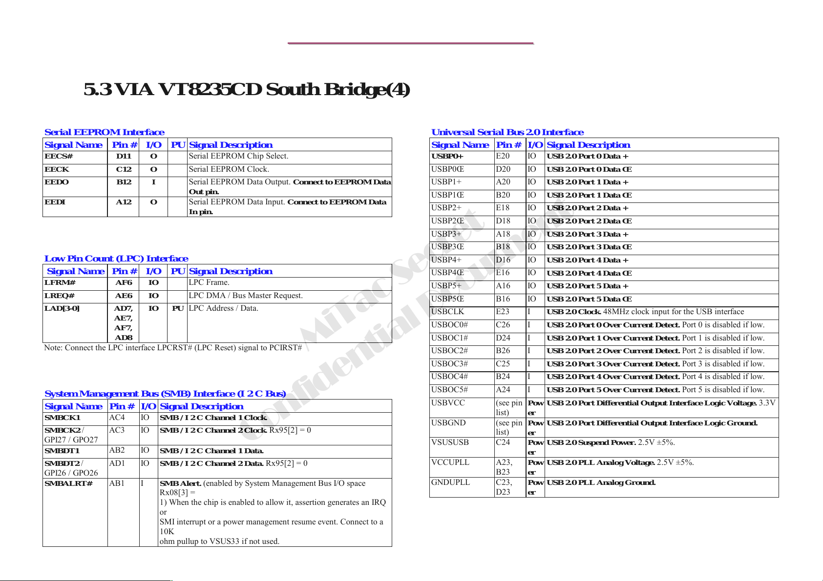
8399
8399
N/B Maintenance
N/B Maintenance
5.3 VIA VT8235CD South Bridge(4)
Serial EEPROM Interface
Signal Name Pin # I/O PU Signal Description
EECS# D11 O
EECK C12 O
EEDO B12 I
EEDI A12 O
Serial EEPROM Chip Select.
Serial EEPROM Clock.
Serial EEPROM Data Output. Connect to EEPROM Data
Out pin.
Serial EEPROM Data Input.
In pin.
Connect to EEPROM Data
Low Pin Count (LPC) Interface
Signal Name Pin # I/O PU Signal Description
LFRM# AF6 IO
LREQ# AE6 IO
LAD[3-0] AD7,
AE7,
AF7,
AD8
Note: Connect the LPC interface LPCRST# (LPC Reset) signal to PCIRST#
IO PU
LPC Frame.
LPC DMA / Bus Master Request.
LPC Address / Data.
System Management Bus (SMB) Interface (I 2 C Bus)
Signal Name Pin # I/O Signal Description
SMBCK1
SMBCK2 /
GPI27 / GPO27
SMBDT1
SMBDT2 /
GPI26 / GPO26
SMBALRT#
AC4 IO
AC3 IO SMB / I 2 C Channel 2 Clock. Rx95[2] = 0
AB2 IO
AD1 IO SMB / I 2 C Channel 2 Data. Rx95[2] = 0
AB1 I SMB Alert. (enabled by System Management Bus I/O space
SMB / I 2 C Channel 1 Clock.
SMB / I 2 C Channel 1 Data.
Rx08[3] =
1) When the chip is enabled to allow it, assertion generates an IRQ
or
SMI interrupt or a power management resume event. Connect to a
10K
ohm pullup to VSUS33 if not used.
Confidential Document
Universal Serial Bus 2.0 Interface
Signal Name Pin # I/O Signal Description
USBP0+
USBP0ΠD20 IO
USBP1+ A20 IO
USBP1ΠB20 IO
USBP2+ E18 IO
USBP2ΠD18 IO
USBP3+ A18 IO
USBP3ΠB18 IO
USBP4+ D16 IO
USBP4ΠE16 IO
USBP5+ A16 IO
USBP5ΠB16 IO
USBCLK E23 I USB 2.0 Clock. 48MHz clock input for the USB interface
USBOC0# C26 I USB 2.0 Port 0 Over Current Detect. Port 0 is disabled if low.
USBOC1# D24 I USB 2.0 Port 1 Over Current Detect. Port 1 is disabled if low.
MiTac Secret
USBOC2# B26 I USB 2.0 Port 2 Over Current Detect. Port 2 is disabled if low.
USBOC3# C25 I USB 2.0 Port 3 Over Current Detect. Port 3 is disabled if low.
USBOC4# B24 I USB 2.0 Port 4 Over Current Detect. Port 4 is disabled if low.
USBOC5# A24 I USB 2.0 Port 5 Over Current Detect. Port 5 is disabled if low.
USBVCC (see pin
USBGND (see pin
VSUSUSB C24
VCCUPLL A23,
GNDUPLL C23,
E20 IO
list)
list)
B23
D23
USB 2.0 Port 0 Data +
USB 2.0 Port 0 Data Œ
USB 2.0 Port 1 Data +
USB 2.0 Port 1 Data Œ
USB 2.0 Port 2 Data +
USB 2.0 Port 2 Data Œ
USB 2.0 Port 3 Data +
USB 2.0 Port 3 Data Œ
USB 2.0 Port 4 Data +
USB 2.0 Port 4 Data Œ
USB 2.0 Port 5 Data +
USB 2.0 Port 5 Data Œ
USB 2.0 Port Differential Output Interface Logic Voltage.
Pow
er
Pow
USB 2.0 Port Differential Output Interface Logic Ground.
er
USB 2.0 Suspend Power. 2.5V ±5%.
Pow
er
USB 2.0 PLL Analog Voltage. 2.5V ±5%.
Pow
er
Pow
USB 2.0 PLL Analog Ground.
er
3.3V
83
Page 85
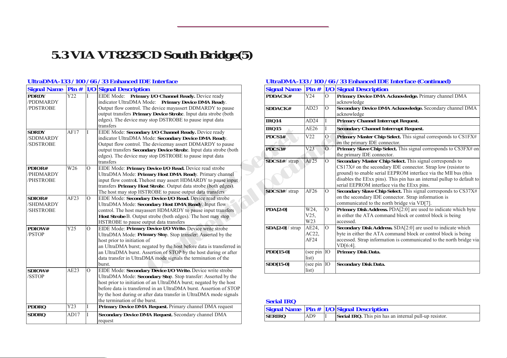
8399
8399
N/B Maintenance
N/B Maintenance
5.3 VIA VT8235CD South Bridge(5)
UltraDMA-133 / 100 / 66 / 33 Enhanced IDE Interface
Signal Name Pin # I/O Signal Description
PDRDY
/PDDMARDY
/PDSTROBE
SDRDY
/SDDMARDY
/SDSTROBE
PDIOR#
/PHDMARDY
/PHSTROBE
SDIOR#
/SHDMARDY
/SHSTROBE
PDIOW#
/PSTOP
SDIOW#
/SSTOP
PDDRQ
SDDRQ
Y22 I EIDE Mode: Primary I/O Channel Ready. Device ready
AF17 I EIDE Mode: Secondary I/O Channel Ready. Device ready
W26 O EIDE Mode: Primary Device I/O Read. Device read strobe
AF23 O EIDE Mode: Secondary Device I/O Read. Device read strobe
Y25 O EIDE Mode:
AE23 O EIDE Mode: Secondary Device I/O Write. Device write strobe
Y23 I Primary Device DMA Request. Primary channel DMA request
AD17 I Secondary Device DMA Request. Secondary channel DMA
indicator UltraDMA Mode: Primary Device DMA Ready.
Output flow control. The device mayassert DDMARDY to pause
output transfers Primary Device Strobe. Input data strobe (both
edges). The device may stop DSTROBE to pause input data
transfers
indicator UltraDMA Mode: Secondary Device DMA Ready.
Output flow control. The devicemay assert DDMARDY to pause
output transfers Secondary Device Strobe. Input data strobe (both
edges). The device may stop DSTROBE to pause input data
transfers
UltraDMA Mode: Primary Host DMA Ready. Primary channel
input flow control. Thehost may assert HDMARDY to pause input
transfers Primary Host Strobe. Output data strobe (both edges).
The host may stop HSTROBE to pause output data transfers
UltraDMA Mode: Secondary Host DMA Ready. Input flow
control. The host mayassert HDMARDY to pause input transfers
Host Strobe B. Output strobe (both edges). The host may stop
HSTROBE to pause output data transfers
Primary Device I /O Write.
UltraDMA Mode:
host prior to initiation of
an UltraDMA burst; negated by the host before data is transferred in
an UltraDMA burst. Assertion of STOP by the host during or after
data transfer in UltraDMA mode signals the termination of the
burst.
UltraDMA Mode: Secondary Stop. Stop transfer: Asserted by the
host prior to initiation of an UltraDMA burst; negated by the host
before data is transferred in an UltraDMA burst. Assertion of STOP
by the host during or after data transfer in UltraDMA mode signals
the termination of the burst.
request
Primary Sto
p. Stop transfer: Asserted by the
Confidential Document
UltraDMA-133 / 100 / 66 / 33 Enhanced IDE Interface (Continued)
Signal Name Pin # I/O Signal Description
PDDACK#
SDDACK#
IRQ14
IRQ15
PDCS1#
PDCS3#
SDCS1# / strap AF25 O Secondary Master Chip Select. This signal corresponds to
SDCS3# / strap AF26 O Secondary Slave Chip Select. This signal corresponds to CS37X#
PDA[2-0]
MiTac Secret
Device write strobe
SDA[2-0] / strap AE24,
PDD[15-0]
SDD[15-0]
Y24 O Primary Device DMA Acknowledge. Primary channel DMA
AD23 O Secondary Device DMA Acknowledge . Secondary channel DMA
AD24 I
AE26 I
V22 O Primary Master Chip Select. This signal corresponds to CS1FX#
V23 O Primary Slave Chip Select. This signal corresponds to CS3FX# on
W24,
V25,
W23
AC22,
AF24
(see pin
list)
(see pin
list)
Serial IRQ
Signal Name Pin # I/O Signal Description
SERIRQ
AD9 I Serial IRQ. This pin has an internal pull-up resistor.
acknowledge
acknowledge
Primary Channel Interrupt Request.
Secondary Channel Interrupt Request.
on the primary IDE connector.
the primary IDE connector.
CS17X# on the secondary IDE connector. Strap low (resistor to
ground) to enable serial EEPROM interface via the MII bus (this
disables the EExx pins). This pin has an internal pullup to default to
serial EEPROM interface via the EExx pins.
on the secondary IDE connector. Strap information is
communicated to the north bridge via VD[7].
O Primary Disk Address. PDA[2:0] are used to indicate which byte
in either the ATA command block or control block is being
accessed.
O Seco ndar y Disk Address. SDA[2:0] are used to indicate which
byte in either the ATA command block or control block is being
accessed. Strap information is communicated to the north bridge via
VD[6:4].
IO
Primary Disk Data.
IO
Secondary Disk Data.
84
Page 86
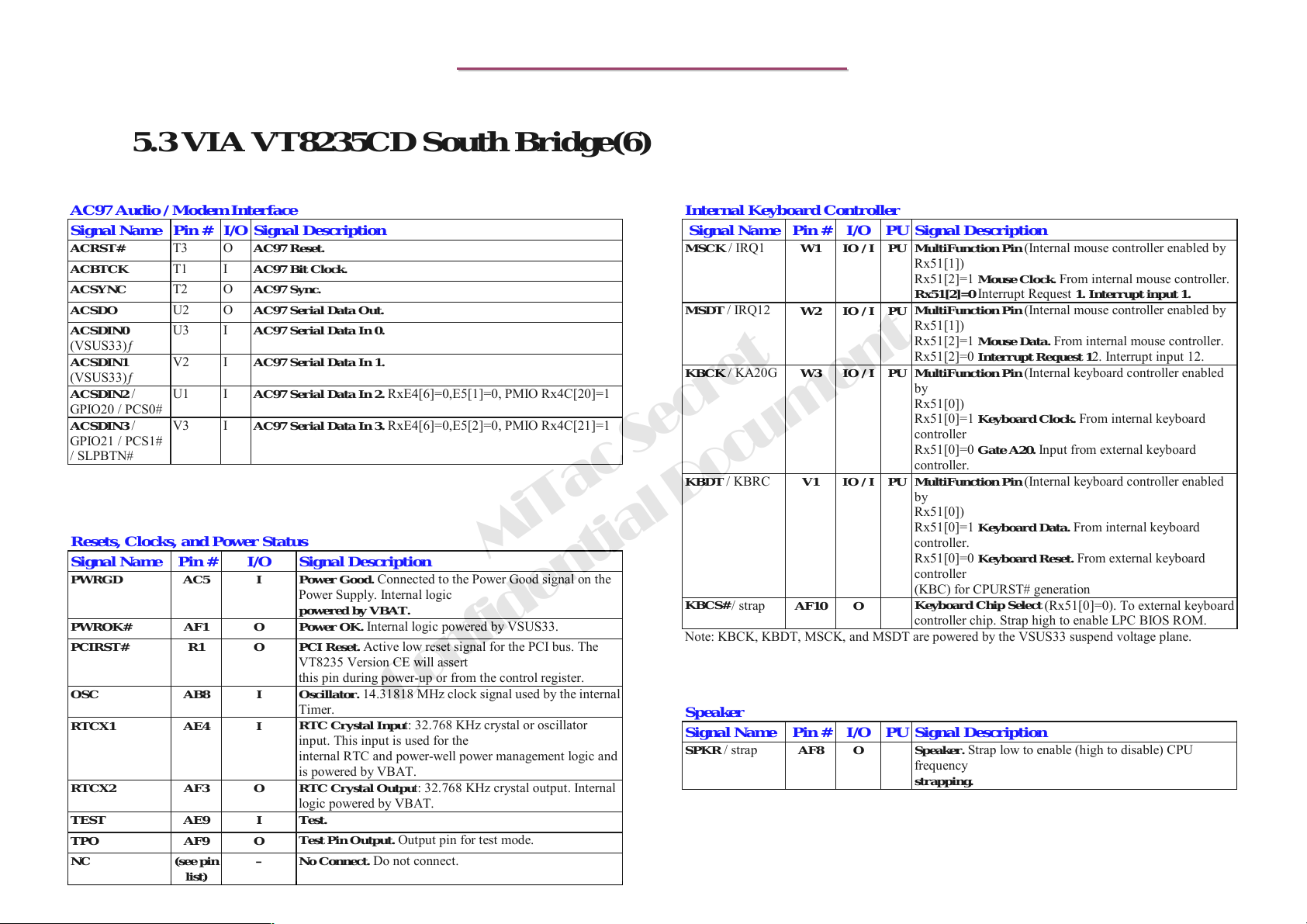
8399
8399
N/B Maintenance
N/B Maintenance
5.3 VIA VT8235CD South Bridge(6)
AC97 Audio / Modem Interface
Signal Name
ACRST#
ACBTCK
ACSYNC
ACSDO
ACSDIN0
(VSUS33)ƒ
ACSDIN1
(VSUS33)ƒ
ACSDIN2 /
GPIO20 / PCS0#
ACSDIN3 /
GPIO21 / PCS1#
/ SLPBTN#
Pin # I/O Signal Description
T3 O
T1 I
T2 O
U2 O
U3 I
V2 I
U1 I AC97 Serial Data In 2. RxE4[6]=0,E5[1]=0, PMIO Rx4C[20]=1
V3 I AC97 Serial Data In 3. RxE4[6]=0,E5[2]=0, PMIO Rx4C[21]=1
AC97 Reset.
AC97 Bit Clock.
AC97 Sync.
AC97 Serial Data Out.
AC97 Serial Data In 0.
AC97 Serial Data In 1.
Resets, Clocks, and Power Status
Signal Name Pin # I/O Signal Description
PWRGD AC5 I
PWROK# AF1 O
PCIRST# R1 O
OSC AB8 I
RTCX1 AE4 I
RTCX2 AF3 O
TEST AE9 I Test.
TPO AF9 O
NC (see pin
list)
Power Good. Connected to the Power Good signal on the
Power Supply. Internal logic
powered by VBAT.
Power OK. Internal logic powered by VSUS33.
PCI Reset. Active low reset signal for the PCI bus. The
VT8235 Version CE will assert
this pin during power-up or from the control register.
Oscillator. 14.31818 MHz clock signal used by the internal
Timer.
RTC Crystal Input: 32.768 KHz crystal or oscillator
input. This input is used for the
internal RTC and power-well power management logic and
is powered by VBAT.
RTC Crystal Output: 32.768 KHz crystal output. Internal
logic powered by VBAT.
Test Pin Output. Output pin for test mode.
No Connect. Do not connect.
–
Confidential Document
Internal Keyboard Controller
Signal Name Pin # I/O PU Signal Description
MSCK / IRQ1
MSDT / IRQ12
KBCK / KA20G
KBDT / KBRC
W1 IO / I PU
W2 IO / I PU
W3 IO / I PU
V1 IO / I PU
MiTac Secret
KBCS#
Note: KBCK, KBDT, MSCK, and MSDT are powered by the VSUS33 suspend voltage plane.
/ strap
AF10 O
MultiFunction Pin (Internal mouse controller enabled by
Rx51[1])
Rx51[2]=1 Mouse Clock. From internal mouse controller.
Rx51[2]=0 Interrupt Request 1. Interrupt input 1.
MultiFunction Pin (Internal mouse controller enabled by
Rx51[1])
Rx51[2]=1 Mouse Data. From internal mouse controller.
Rx51[2]=0 Interrupt Request 12. Interrupt input 12.
MultiFunction Pin (Internal keyboard controller enabled
by
Rx51[0])
Rx51[0]=1 Keyboard Clock. From internal keyboard
controller
Rx51[0]=0 Gate A20. Input from external keyboard
controller.
MultiFunction Pin (Internal keyboard controller enabled
by
Rx51[0])
Rx51[0]=1 Keyboard Data. From internal keyboard
controller.
Rx51[0]=0 Keyboard Reset. From external keyboard
controller
(KBC) for CPURST# generation
Keyboard Chip Select
controller chip. Strap high to enable LPC BIOS ROM.
(Rx51[0]=0). To external keyboard
Speaker
Signal Name Pin # I/O PU Signal Description
SPKR / strap
AF8 O
Speaker. Strap low to enable (high to disable) CPU
frequency
strapping.
85
Page 87
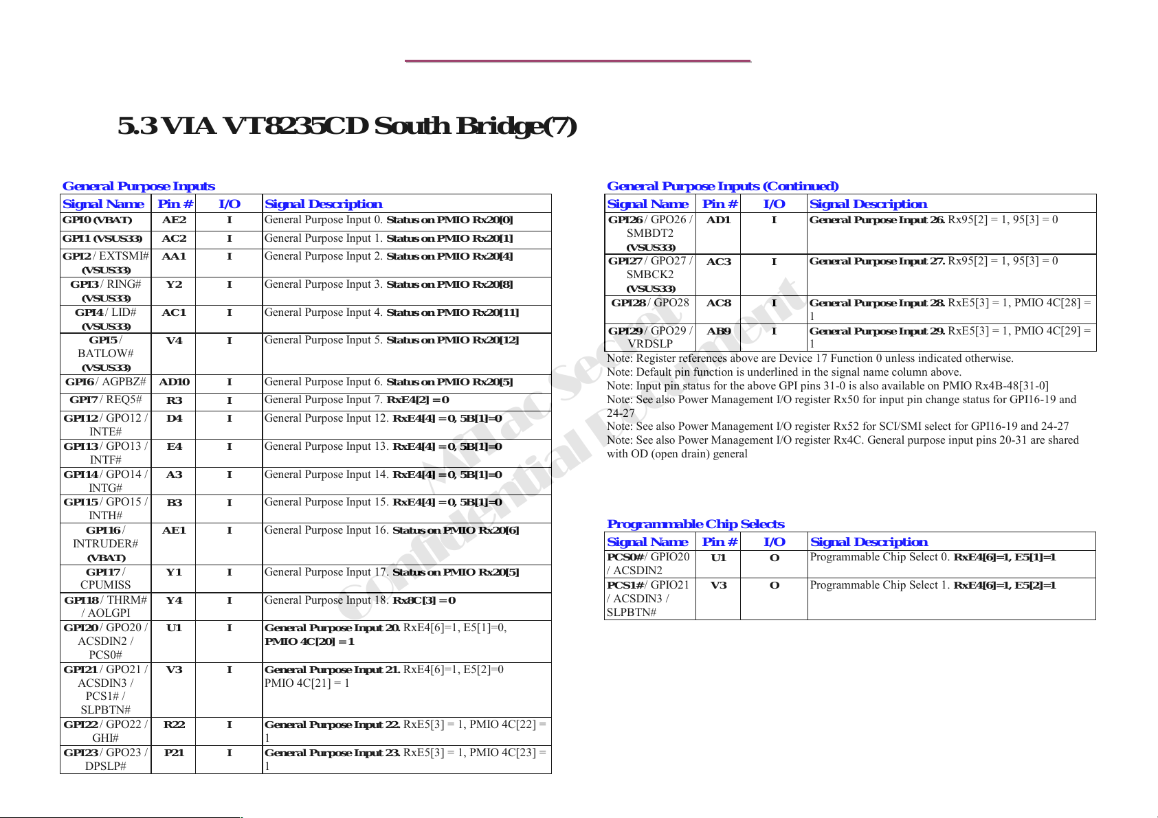
8399
8399
N/B Maintenance
N/B Maintenance
5.3 VIA VT8235CD South Bridge(7)
General Purpose Inputs
Signal Name Pin # I/O Signal Description
GPI0 (VBAT) AE2 I
GPI1 (VSUS33) AC2 I
GPI2 / EXTSMI#
(VSUS33)
GPI3 / RING#
(VSUS33)
GPI4 / LID#
(VSUS33)
GPI5 /
BATLOW#
(VSUS33)
GPI6 / AGPBZ#
GPI7 / REQ5#
GPI12 / GPO12 /
INTE#
GPI13 / GPO13 /
INTF#
GPI14 / GPO14 /
INTG#
GPI15 / GPO15 /
INTH#
GPI16 /
INTRUDER#
(VBAT)
GPI17 /
CPUMISS
GPI18 / THRM#
/ AOLGPI
GPI20 / GPO20 /
ACSDIN2 /
PCS0#
GPI21 / GPO21 /
ACSDIN3 /
PCS1# /
SLPBTN#
GPI22 / GPO22 /
GPI23 / GPO23 /
GHI#
DPSLP#
AA1 I
Y2 I
AC1 I
V4 I
AD10 I
R3 I
D4 I
E4 I
A3 I
B3 I
AE1 I
Y1 I
Y4 I
U1 I
V3 I
R22 I
P21 I
General Purpose Input 0. Status on PMIO Rx20[0]
General Purpose Input 1. Status on PMIO Rx20[1]
General Purpose Input 2. Status on PMIO Rx20[4]
General Purpose Input 3. Status on PMIO Rx20[8]
General Purpose Input 4. Status on PMIO Rx20[11]
General Purpose Input 5. Status on PMIO Rx20[12]
General Purpose Input 6. Status on PMIO Rx20[5]
General Purpose Input 7. RxE4[2] = 0
General Purpose Input 12. RxE4[4] = 0, 5B[1]=0
General Purpose Input 13. RxE4[4] = 0, 5B[1]=0
General Purpose Input 14. RxE4[4] = 0, 5B[1]=0
General Purpose Input 15. RxE4[4] = 0, 5B[1]=0
General Purpose Input 16. Status on PMIO Rx20[6]
General Purpose Input 17. Status on PMIO Rx20[5]
General Purpose Input 18. Rx8C[3] = 0
General Purpose Input 20. RxE4[6]=1, E5[1]=0,
PMIO 4C[20] = 1
General Purpose Input 21. RxE4[6]=1, E5[2]=0
PMIO 4C[21] = 1
General Purpose Input 22. RxE5[3] = 1, PMIO 4C[22] =
1
General Purpose Input 23. RxE5[3] = 1, PMIO 4C[23] =
1
Confidential Document
General Purpose Inputs (Continued)
Signal Name Pin # I/O Signal Description
GPI26 / GPO26 /
SMBDT2
(VSUS33)
GPI27 / GPO27 /
SMBCK2
(VSUS33)
GPI28 / GPO28
GPI29 / GPO29 /
VRDSLP
Note: Register references above are Device 17 Function 0 unless indicated otherwise.
Note: Default pin function is underlined in the signal name column above.
Note: Input pin status for the above GPI pins 31-0 is also available on PMIO Rx4B-48[31-0]
Note: See also Power Management I/O register Rx50 for input pin change status for GPI16-19 and
24-27
Note: See also Power Management I/O register Rx52 for SCI/SMI select for GPI16-19 and 24-27
Note: See also Power Management I/O register Rx4C. General purpose input pins 20-31 are shared
with OD (open drain) general
AD1 I
AC3 I
AC8 I
AB9 I
MiTac Secret
Programmable Chip Selects
Signal Name Pin # I/O Signal Description
PCS0# / GPIO20
/ ACSDIN2
PCS1# / GPIO21
/ ACSDIN3 /
SLPBTN#
U1 O
V3 O
General Purpose Input 26. Rx95[2] = 1, 95[3] = 0
General Purpose Input 27. Rx95[2] = 1, 95[3] = 0
General Purpose Input 28. RxE5[3] = 1, PMIO 4C[28] =
1
General Purpose Input 29. RxE5[3] = 1, PMIO 4C[29] =
1
Programmable Chip Select 0. RxE4[6]=1, E5[1]=1
Programmable Chip Select 1. RxE4[6]=1, E5[2]=1
86
Page 88
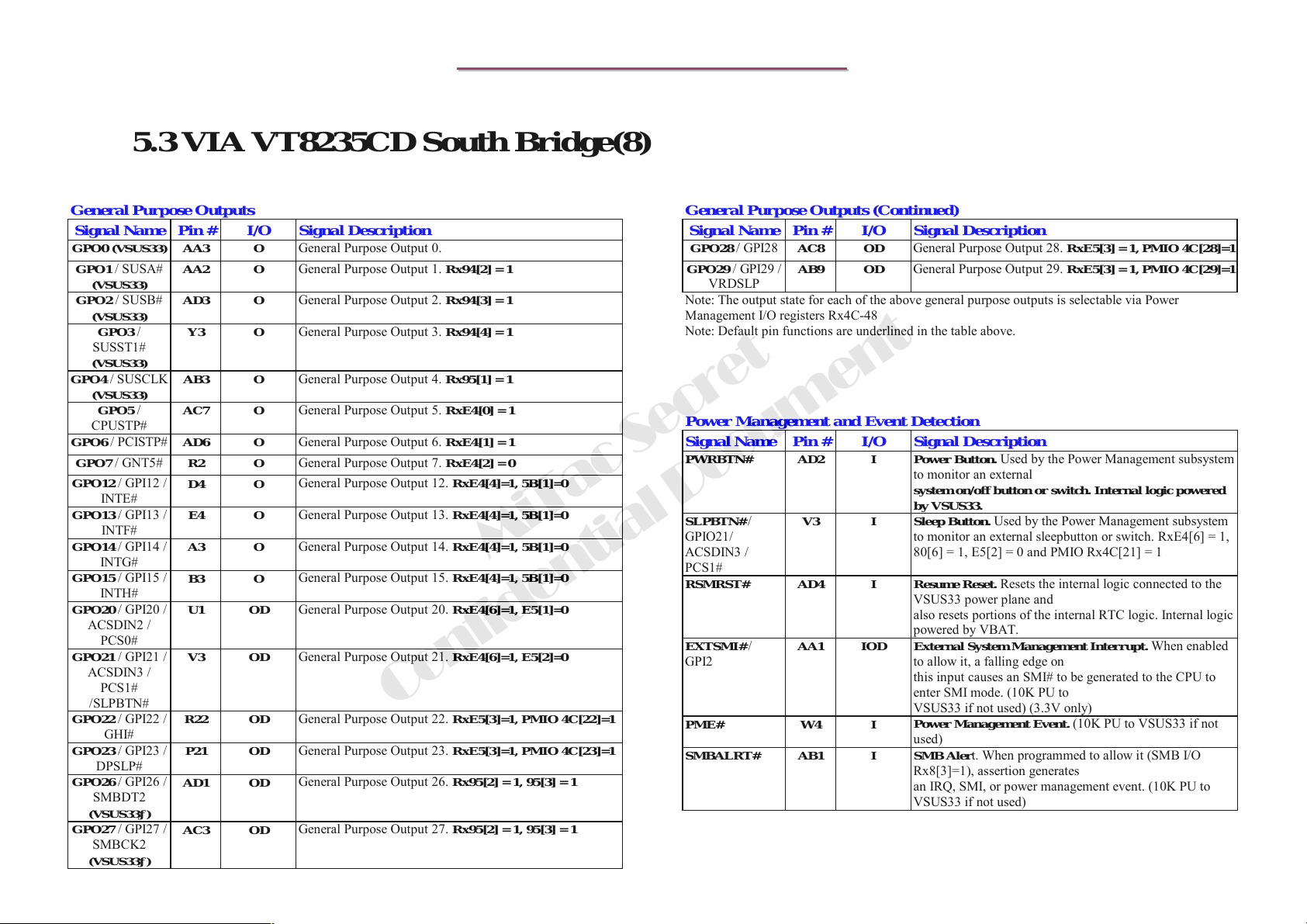
8399
8399
N/B Maintenance
N/B Maintenance
5.3 VIA VT8235CD South Bridge(8)
General Purpose Outputs
Signal Name Pin # I/O Signa l Description
GPO0 (VSUS33) AA3 O
GPO1 / SUSA#
(VSUS33)
GPO2 / SUSB#
(VSUS33)
GPO3 /
SUSST1#
(VSUS33)
GPO4 / SUSCLK
(VSUS33)
GPO5 /
CPUSTP#
GPO6 / PCISTP#
GPO7 / GNT5#
GPO12 / GPI12 /
INTE#
GPO13 / GPI13 /
INTF#
GPO14 / GPI14 /
INTG#
GPO15 / GPI15 /
INTH#
GPO20 / GPI20 /
ACSDIN2 /
PCS0#
GPO21 / GPI21 /
ACSDIN3 /
PCS1#
/SLPBTN#
GPO22 / GPI22 /
GHI#
GPO23 / GPI23 /
DPSLP#
GPO26 / GPI26 /
SMBDT2
(VSUS33ƒ)
GPO27 / GPI27 /
SMBCK2
(VSUS33ƒ)
AA2 O
AD3 O
Y3 O
AB3 O
AC7 O
AD6 O
R2 O
D4 O
E4 O
A3 O
B3 O
U1 OD
V3 OD
R22 OD
P21 OD
AD1 OD
AC3 OD
General Purpose Output 0.
General Purpose Output 1. Rx94[2] = 1
General Purpose Output 2. Rx94[3] = 1
General Purpose Output 3. Rx94[4] = 1
General Purpose Output 4. Rx95[1] = 1
General Purpose Output 5. RxE4[0] = 1
General Purpose Output 6. RxE4[1] = 1
General Purpose Output 7. RxE4[2] = 0
General Purpose Output 12. RxE4[4]=1, 5B[1]=0
General Purpose Output 13. RxE4[4]=1, 5B[1]=0
General Purpose Output 14. RxE4[4]=1, 5B[1]=0
General Purpose Output 15. RxE4[4]=1, 5B[1]=0
General Purpose Output 20. RxE4[6]=1, E5[1]=0
General Purpose Output 21. RxE4[6]=1, E5[2]=0
Confidential Document
General Purpose Output 22. RxE5[3]=1, PMIO 4C[22]=1
General Purpose Output 23. RxE5[3]=1, PMIO 4C[23]=1
General Purpose Output 26. Rx95[2] = 1, 95[3] = 1
General Purpose Output 27. Rx95[2] = 1, 95[3] = 1
General Purpose Outputs (Continued)
Signal Name Pin # I/O Signal De scriptio n
GPO28 / GPI28
GPO29 / GPI29 /
VRDSLP
Note: The output state for each of the above general purpose outputs is selectable via Power
Management I/O registers Rx4C-48
Note: Default pin functions are underlined in the table above.
AC8 OD
AB9 OD
Power Management and Event Detection
Signal Name Pin # I/O Signal Description
PWRBTN# AD2 I
SLPBTN# /
GPIO21/
MiTac Secret
ACSDIN3 /
PCS1#
RSMRST# AD4 I
EXTSMI# /
GPI2
PME# W4 I
SMBALRT# AB1 I
V3 I
AA1 IOD
General Purpose Output 28. RxE5[3] = 1, PMIO 4C[28]=1
General Purpose Output 29. RxE5[3] = 1, PMIO 4C[29]=1
Power Button. Used by the Power Management subsystem
to monitor an external
system on/off button or switch. Internal logic powered
by VSUS33.
Sleep Button. Used by the Power Management subsystem
to monitor an external sleepbutton or switch. RxE4[6] = 1,
80[6] = 1, E5[2] = 0 and PMIO Rx4C[21] = 1
Resume Reset. Resets the internal logic connected to the
VSUS33 power plane and
also resets portions of the internal RTC logic. Internal logic
powered by VBAT.
External System Management Interrupt. When enabled
to allow it, a falling edge on
this input causes an SMI# to be generated to the CPU to
enter SMI mode. (10K PU to
VSUS33 if not used) (3.3V only)
Power Management Event. (10K PU to VSUS33 if not
used)
SMB Alert. When programmed to allow it (SMB I/O
Rx8[3]=1), assertion generates
an IRQ, SMI, or power management event. (10K PU to
VSUS33 if not used)
87
Page 89
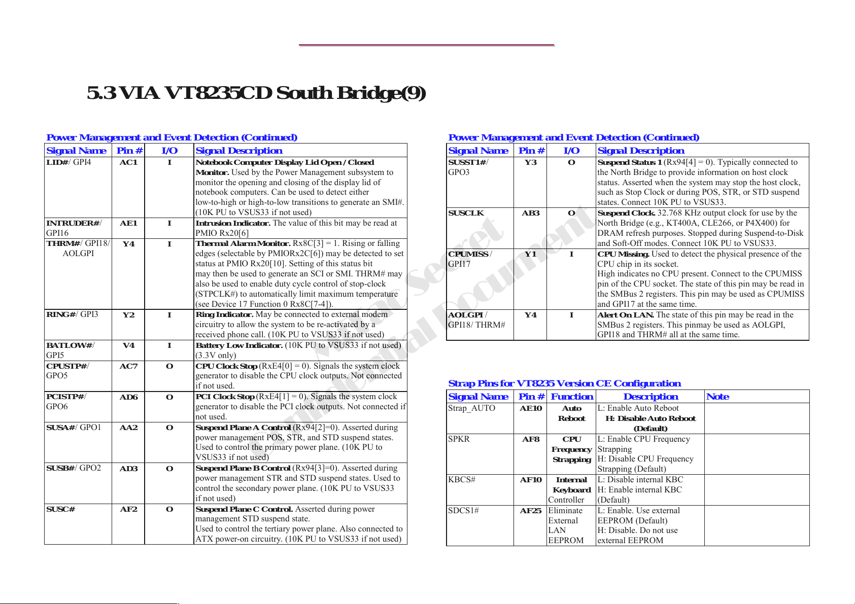
8399
8399
N/B Maintenance
N/B Maintenance
5.3 VIA VT8235CD South Bridge(9)
Power Management and Event Detection (Continued)
Signal Name Pin # I/O Signal Description
LID# / GPI4
INTRUDER# /
GPI16
THRM# / GPI18/
AOLGPI
RING# / GPI3
BATLOW# /
GPI5
CPUSTP# /
GPO5
PCISTP#
GPO6
SUSA# / GPO1
SUSB# / GPO2
SUSC# AF2 O
/
AC1 I Notebook Computer Display Lid Open / Closed
AE1 I
Y4 I
Y2 I
V4 I
AC7 O
AD6 O
AA2 O
AD3 O
Monitor. Used by the Power Management subsystem to
monitor the opening and closing of the display lid of
notebook computers. Can be used to detect either
low-to-high or high-to-low transitions to generate an SMI#.
(10K PU to VSUS33 if not used)
Intrusion Indicator. The value of this bit may be read at
PMIO Rx20[6]
Therma l Al arm Monito r. Rx8C[3] = 1. Rising or falling
edges (selectable by PMIORx2C[6]) may be detected to set
status at PMIO Rx20[10]. Setting of this status bit
may then be used to generate an SCI or SMI. THRM# may
also be used to enable duty cycle control of stop-clock
(STPCLK#) to automatically limit maximum temperature
(see Device 17 Function 0 Rx8C[7-4]).
Ring Indicator. May be connected to external modem
circuitry to allow the system to be re-activated by a
received phone call. (10K PU to VSUS33 if not used)
Battery Low Indicator. (10K PU to VSUS33 if not used)
(3.3V only)
CPU Clock Stop (RxE4[0] = 0). Signals the system clock
generator to disable the CPU clock outputs. Not connected
if not used.
PCI Clock Stop
generator to disable the PCI clock outputs. Not connected if
not used.
Suspend Plane A Control (Rx94[2]=0). Asserted during
power management POS, STR, and STD suspend states.
Used to control the primary power plane. (10K PU to
VSUS33 if not used)
Suspend Plane B Control (Rx94[3]=0). Asserted during
power management STR and STD suspend states. Used to
control the secondary power plane. (10K PU to VSUS33
if not used)
Suspend Plane C Control. Asserted during power
management STD suspend state.
Used to control the tertiary power plane. Also connected to
ATX power-on circuitry. (10K PU to VSUS33 if not used)
(RxE4[1] = 0). Signals the system clock
Confidential Document
Power Management and Event Detection (Continued)
Signal Name Pin # I/O Signal Description
SUSST1# /
GPO3
SUSCLK AB3 O
CPUMISS /
GPI17
AOLGPI
GPI18/ THRM#
/
MiTac Secret
Strap Pins for VT8235 Version CE Configuration
Signal Name Pin # Function Description Note
Strap_AUTO
SPKR
KBCS#
SDCS1#
AE10 Auto
AF10 Internal
AF25
Y3 O
Y1 I
Y4 I
Reboot
AF8 CPU
Frequency
Strapping
Keyboard
Controller
Eliminate
External
LAN
EEPROM
Suspend Status 1 (Rx94[4] = 0). Typically connected to
the North Bridge to provide information on host clock
status. Asserted when the system may stop the host clock,
such as Stop Clock or during POS, STR, or STD suspend
states. Connect 10K PU to VSUS33.
Suspend Clock.
North Bridge (e.g., KT400A, CLE266, or P4X400) for
DRAM refresh purposes. Stopped during Suspend-to-Disk
and Soft-Off modes. Connect 10K PU to VSUS33.
CPU Missing. Used to detect the physical presence of the
CPU chip in its socket.
High indicates no CPU present. Connect to the CPUMISS
pin of the CPU socket. The state of this pin may be read in
the SMBus 2 registers. This pin may be used as CPUMISS
and GPI17 at the same time.
Alert On LAN.
SMBus 2 registers. This pinmay be used as AOLGPI,
GPI18 and THRM# all at the same time.
L: Enable Auto Reboot
H: Disable Auto Reboot
L: Enable CPU Frequency
Strapping
H: Disable CPU Frequency
Strapping (Default)
L: Disable internal KBC
H: Enable internal KBC
(Default)
L: Enable. Use external
EEPROM (Default)
H: Disable. Do not use
external EEPROM
32.768 KHz output clock for use by the
The state of this pin may be read in the
(Default)
88
Page 90
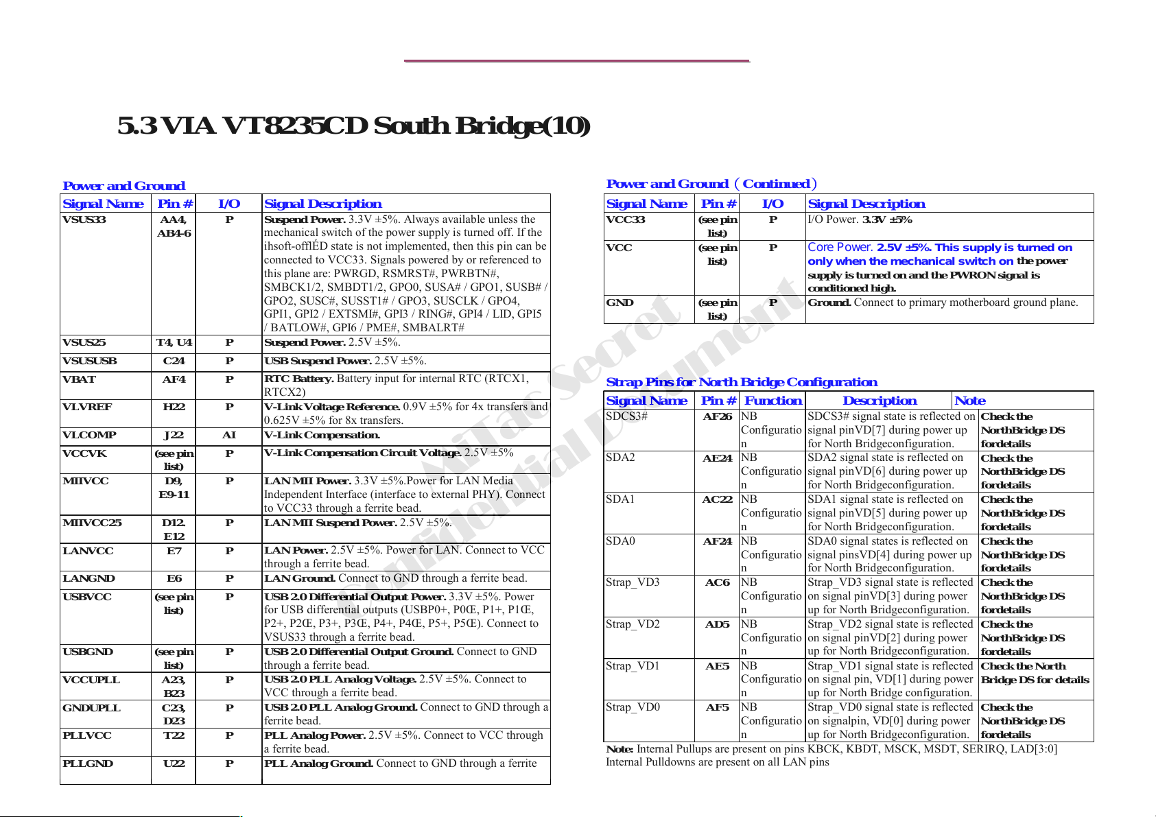
8399
8399
N/B Maintenance
N/B Maintenance
5.3 VIA VT8235CD South Bridge(10)
Power and Ground
Signal Name Pin # I/O Signal Description
VSUS33 AA4,
AB4-6
VSUS25 T4, U4 P
VSUSUSB C24 P
VBAT AF4 P
VLVREF H22 P
VLCOMP J22 AI V-Link Compensation.
VCCVK (see pin
list)
MIIVCC D9,
E9-11
MIIVCC25 D12.
E12
LANVCC E7 P
LANGND E6 P
USBVCC (see pin
list)
USBGND (see pin
list)
VCCUPLL A23,
B23
GNDUPLL C23,
D23
PLLVCC T22 P
PLLGND U22 P
Suspend Power. 3.3V ±5%. Always available unless the
P
mechanical switch of the power supply is turned off. If the
ihsoft-offlÉD state is not implemented, then this pin can be
connected to VCC33. Signals powered by or referenced to
this plane are: PWRGD, RSMRST#, PWRBTN#,
SMBCK1/2, SMBDT1/2, GPO0, SUSA# / GPO1, SUSB# /
GPO2, SUSC#, SUSST1# / GPO3, SUSCLK / GPO4,
GPI1, GPI2 / EXTSMI#, GPI3 / RING#, GPI4 / LID, GPI5
/ BATLOW#, GPI6 / PME#, SMBALRT#
Suspend Power. 2.5V ±5%.
USB Suspend Power. 2.5V ±5%.
RTC Battery. Battery input for internal RTC (RTCX1,
RTCX2)
V-Link Voltage Reference. 0.9V ±5% for 4x transfers and
0.625V ±5% for 8x transfers.
V-Link Compensation Circuit Voltage. 2.5V ±5%
P
LAN MII Power. 3.3V ±5%.Power for LAN Media
P
Independent Interface (interface to external PHY). Connect
to VCC33 through a ferrite bead.
LAN MII Suspend Power. 2.5V ±5%.
P
LAN Power. 2.5V ±5%. Power for LAN. Connect to VCC
through a ferrite bead.
LAN Ground. Connect to GND through a ferrite bead.
USB 2.0 Differential Output Power. 3.3V ±5%. Power
P
for USB differential outputs (USBP0+, P0Œ, P1+, P1Œ,
P2+, P2Œ, P3+, P3Œ, P4+, P4Œ, P5+, P5Œ). Connect to
VSUS33 through a ferrite bead.
USB 2.0 Differential Output Ground. Connect to GND
P
through a ferrite bead.
USB 2.0 PLL Analog Voltage. 2.5V ±5%. Connect to
P
VCC through a ferrite bead.
USB 2.0 PLL Analog Ground. Connect to GND through a
P
ferrite bead.
PLL Analog Power. 2.5V ±5%. Connect to VCC through
a ferrite bead.
PLL Analog Ground. Connect to GND through a ferrite
bead.
Confidential Document
Power and Ground
Signal Name Pin # I/O Signal Description
VCC33 (see pin
VCC (see pin
GND (see pin
Strap Pins for North Bridge Configuration
Signal Name Pin # Function Description Note
SDCS3#
SDA2
MiTac Secret
SDA1
SDA0
Strap_VD3
Strap_VD2
Strap_VD1
Strap_VD0
Note: Internal Pullups are present on pins KBCK, KBDT, MSCK, MSDT, SERIRQ, LAD[3:0]
Internal Pulldowns are present on all LAN pins
AF26
AE24
AC22
AF24
list)
list)
list)
AC6
AD5
AE5
AF5
Continued
((((
P
P Core Power. 2.5V ±5%. This supply is turned on
P
NB
Configuratio
n
NB
Configuratio
n
NB
Configuratio
n
NB
Configuratio
n
NB
Configuratio
n
NB
Configuratio
n
NB
Configuratio
n
NB
Configuratio
n
))))
I/O Power. 3.3V ±5%
only when the mechanical switch on
supply is turned on and the PWRON signal is
conditioned high.
Ground. Connect to primary motherboard ground plane.
SDCS3# signal state is reflected on
signal pinVD[7] during power up
for North Bridgeconfiguration.
SDA2 signal state is reflected on
signal pinVD[6] during power up
for North Bridgeconfiguration.
SDA1 signal state is reflected on
signal pinVD[5] during power up
for North Bridgeconfiguration.
SDA0 signal states is reflected on
signal pinsVD[4] during power up
for North Bridgeconfiguration.
Strap_VD3 signal state is reflected
on signal pinVD[3] during power
up for North Bridgeconfiguration.
Strap_VD2 signal state is reflected
on signal pinVD[2] during power
up for North Bridgeconfiguration.
Strap_VD1 signal state is reflected
on signal pin, VD[1] during power
up for North Bridge configuration.
Strap_VD0 signal state is reflected
on signalpin, VD[0] during power
up for North Bridgeconfiguration.
Check the
NorthBridge DS
fordetails
Check the
NorthBridge DS
fordetails
Check the
NorthBridge DS
fordetails
Check the
NorthBridge DS
fordetails
Check the
NorthBridge DS
fordetails
Check the
NorthBridge DS
fordetails
Check the North
Bridge DS for details
Check the
NorthBridge DS
fordetails
the power
89
Page 91
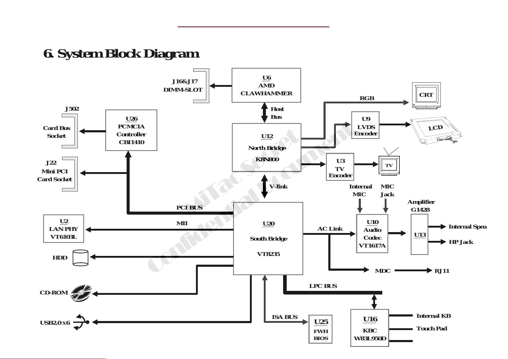
8399
8399
6. System Block Diagram
N/B Maintenance
N/B Maintenance
J502
Card Bus
Socket
J22
Mini PCI
Card Socket
U2
LAN PHY
VT6103L
HDD
U26
PCMCIA
Controller
CBI1410
J16&J17
DIMM-SLOT
PCI BUS
MiTac Secret
MII
U6
AMD
CLAWHAMMER
Host
Bus
U12
North Bridge
K8N800
V-link
U20
South Bridge
VT8235
U3
TV
Encoder
AC Link
RGB
U9
LVDS
Encoder
Internal
MIC
U10
Audio
Codec
VT1617A
TV
MIC
Jack
CRT
L
L
Amplifier
G1428
U13
D
D
C
C
Internal Speaker
HP Jack
CD-ROM
USB2.0
X6
Confidential Document
LPC BUS
ISA BUS
U25
FWH
BIOS
W83L950D
MDC
U16
KBC
RJ11
Internal KB
Touch Pad
FAN
90
Page 92

8399
8399
7. Maintenance Diagnostics
7.1 Introduction
Each time the computer is turned on, the system BIOS runs a series of internal checks on the hardware. This power-
on self test (post) allows the computer to detect problems as early as the power-on stage. Error messages of post can
alert you to the problems of your computer.If an error is detected during these tests, you will see an error message
displayed on the screen. If the error occurs before the display is initialized, then the screen cannot display the error
message. Error codes or system beeps are used to identify a post error that occurs when the screen is not available.
The value for the diagnostic port is written at the beginning of the test. Therefore, if the test failed, the user can
N/B Maintenance
N/B Maintenance
determine where the problem occurred by reading the last value written to the port by the debug card plug at MINI
PCI slot.
MiTac Secret
Confidential Document
91
Page 93
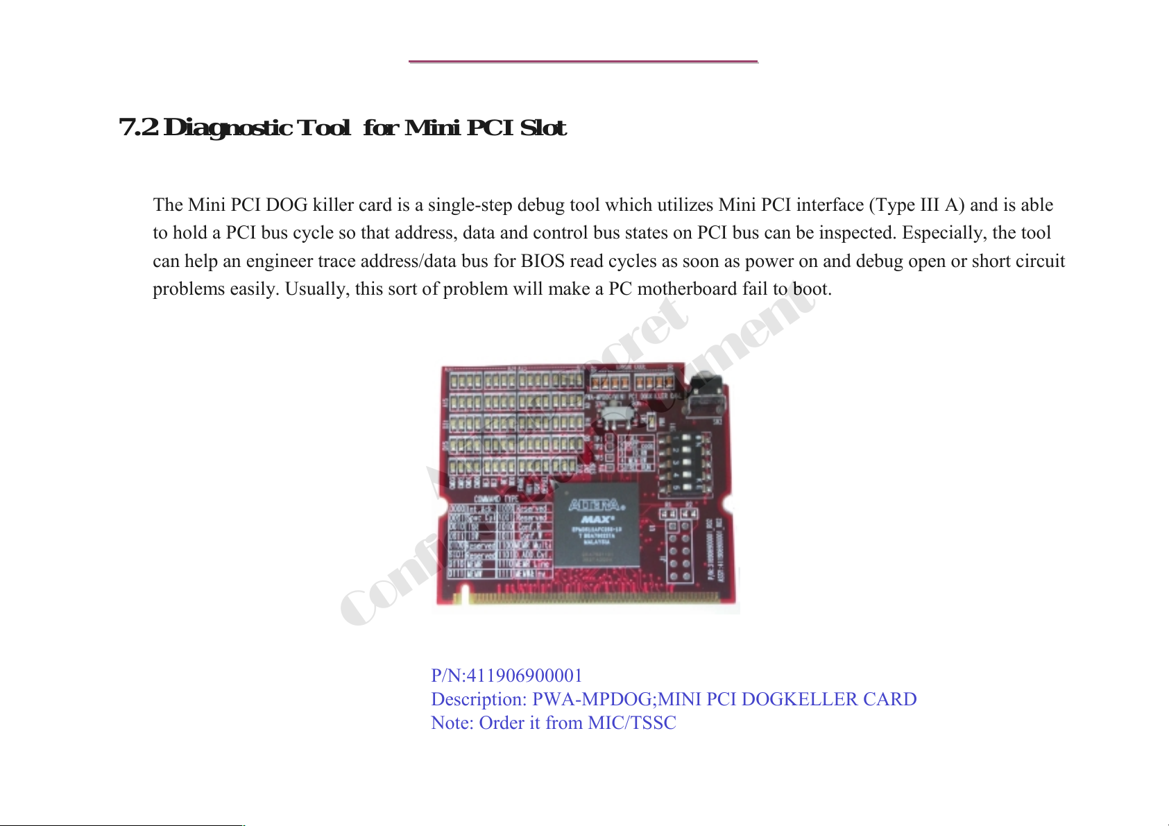
8399
8399
N/B Maintenance
N/B Maintenance
7.2 Diagnostic Tool for Mini PCI Slot
The Mini PCI DOG killer card is a single-step debug tool which utilizes Mini PCI interface (Type III A) and is able
to hold a PCI bus cycle so that address, data and control bus states on PCI bus can be inspected. Especially, the tool
can help an engineer trace address/data bus for BIOS read cycles as soon as power on and debug open or short circuit
problems easily. Usually, this sort of problem will make a PC motherboard fail to boot.
MiTac Secret
Confidential Document
P/N:411906900001
Description: PWA-MPDOG;MINI PCI DOGKELLER CARD
Note: Order it from MIC/TSSC
92
Page 94
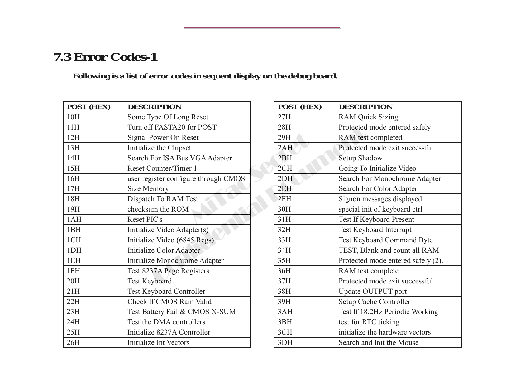
7.3 Error Codes-1
Following is a list of error code s in sequent display on the debug board.
8399
8399
N/B Maintenance
N/B Maintenance
POST (HEX) DE SCRIPTION
10H Some Type Of Long Reset
11H Turn off FASTA20 for POST
12H Signal Power On Reset
13H Initialize the Chipset
14H Search For ISA Bus VGA Adapter
15H Reset Counter/Timer 1
16H user register configure through CMOS
17H Size Memory
18H Dispatch To RAM Test
19H checksum the ROM
1AH Reset PIC's
1BH Initialize Video Adapter(s)
1CH Initialize Video (6845 Regs)
1DH Initialize Color Adapter
1EH Initialize Monochrome Adapter
1FH Test 8237A Page Registers
20H Test Keyboard
21H Test Keyboard Controller
22H Check If CMOS Ram Valid
23H Test Battery Fail & CMOS X-SUM
24H Test the DMA controllers
25H Initialize 8237A Controller
26H Initialize Int Vectors
Confidential Document
MiTac Secret
POST (HEX) DESCRIPTION
27H RAM Quick Sizing
28H Protected mode entered safely
29H RAM test completed
2AH Protected mode exit successful
2BH Setup Shadow
2CH Going To Initialize Video
2DH Search For Monochrome Adapter
2EH Search For Color Adapter
2FH Signon messages displayed
30H special init of keyboard ctrl
31H Test If Keyboard Present
32H Test Keyboard Interrupt
33H Test Keyboard Command Byte
34H TEST, Blank and count all RAM
35H Protected mode entered safely (2).
36H RAM test complete
37H Protected mode exit successful
38H Update OUTPUT port
39H Setup Cache Controller
3AH Test If 18.2Hz Periodic Working
3BH test for RTC ticking
3CH initialize the hardware vectors
3DH Search and Init the Mouse
93
Page 95
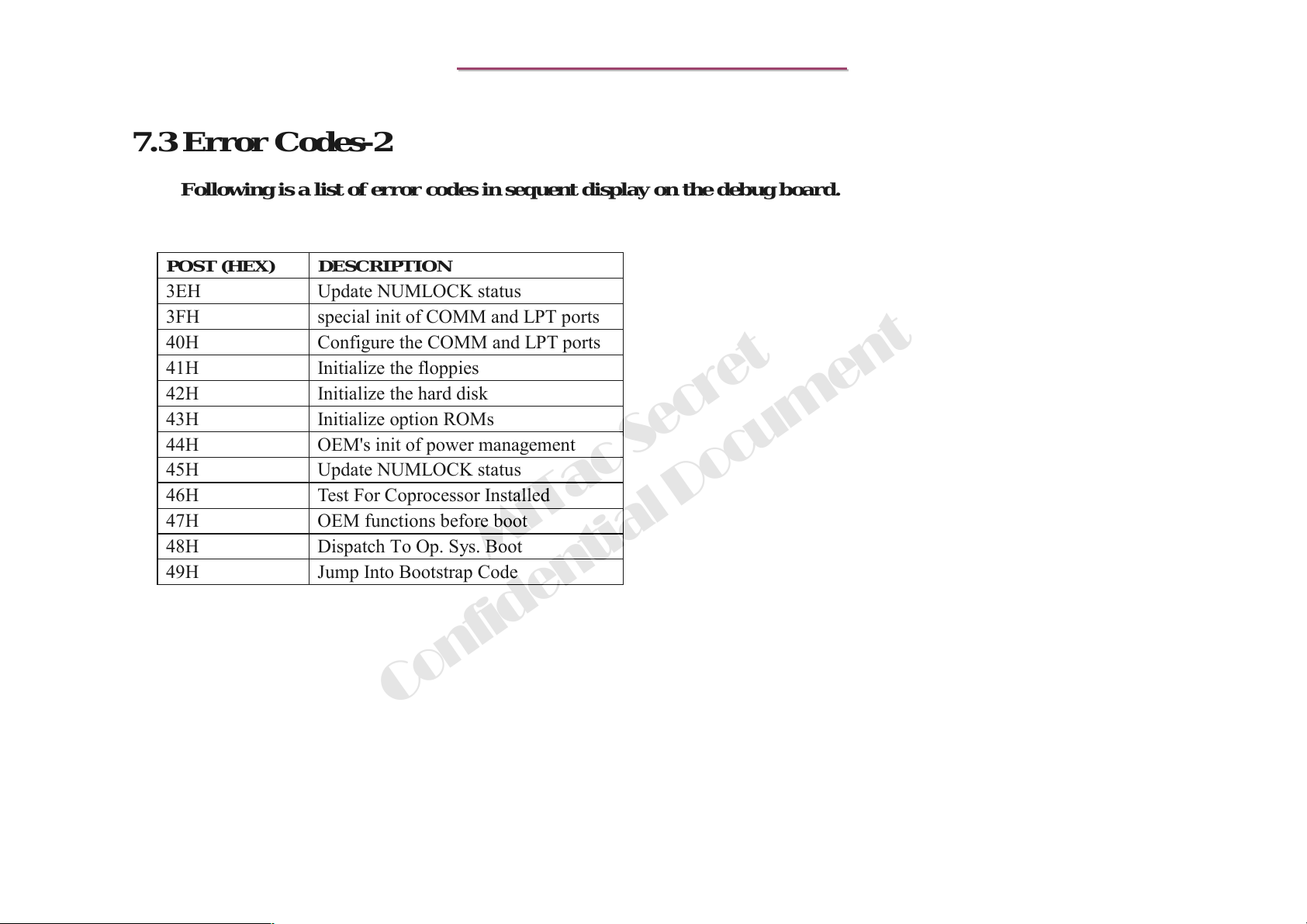
8399
8399
N/B Maintenance
N/B Maintenance
7.3 Error Codes-2
Following is a list of error code s in sequent display on the debug board.
POST (HEX) DESCRIPTION
3EH Update NUMLOCK status
3FH special init of COMM and LPT ports
40H Configure the COMM and LPT ports
41H Initialize the floppies
42H Initialize the hard disk
43H Initialize option ROMs
44H OEM's init of power management
45H Update NUMLOCK status
46H Test For Coprocessor Installed
47H OEM functions before boot
48H Dispatch To Op. Sys. Boot
49H Jump Into Bootstrap Code
MiTac Secret
Confidential Document
94
Page 96
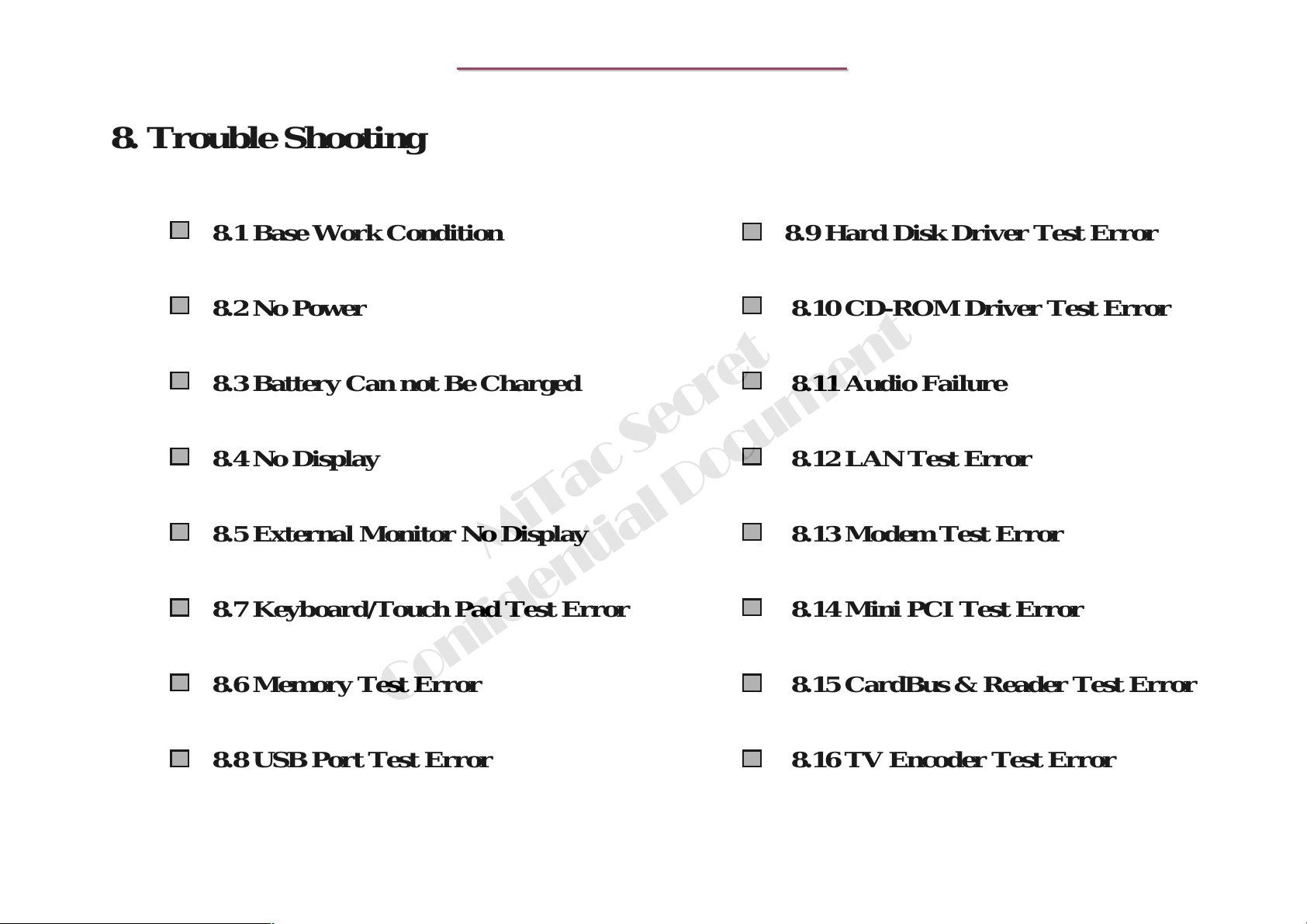
8. Trouble Shooting
8399
8399
N/B Maintenance
N/B Maintenance
8.1 Base Work Condition
8.2 No Power
8.3 Battery Can not Be Charged
8.4 No Display
8.5 External Monitor No Display
MiTac Secret
8.7 Keyboard/Touch Pad Test Error
8.9 Hard Disk Driver Test Error
8.10 CD-ROM Driver Test Error
8.11 Audio Failure
8.12 LAN Test Error
8.13 Modem Test Error
8.14 Mini PCI Test Error
8.6 Memory Test Error
Confidential Document
8.8 USB Port Test Error
8.15 CardBus & Reader Test Error
8.16 TV Encoder Test Error
95
Page 97
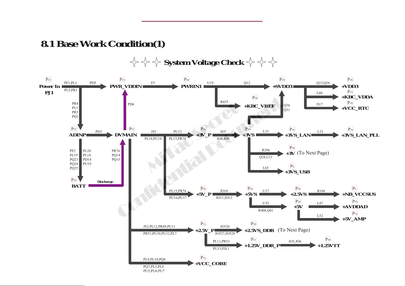
8399
8399
8.1 Base Work Condition(1)
N/B Maintenance
N/B Maintenance
System Voltage Check
P23
Power In
PJ1
PF1,PL1 PD5
PL5,PR1
PR4
PU1
PR3
PQ1
ADINP DVMAIN
PF2
PL19
PQ23
PQ24
PQ25
P24
PD3
PL20
PL18
PD14
PU19
Discharge
P23
PWR_VDDIN
PR76
PQ14
PQ15
BATT
Confidential Document
PD6
P23P23
F5
P20
PWRIN1
U19
R435
Q12
P20
+KBC_VREF
JS5
PU15
P26
JO7
JO8,JO9PL13,PR73PL14,PU14
P20
+3VS+3V_P
MiTac Secret
PL15,PR74 JO10
+5V_P
+2.5V_P
JO11,JO12PU16,PU17
JO526JS3,PL12,PR49,PU11
JO527,JO528PR51,PU10,PU12,PL7
PL11,PR53
PU13,PJL1
P20P26
+5VS
P20P21
+2.5VS_DDR
P21
+1.25V_DDR_P
L33
R296
Q28,U21
L65
U17
U35
R408,Q41
P20
+SVDD3
Q36
Q31
P16 P16
+3VS_LAN
P20
+3V
P8
+3VS_USB
+2.5VS
+5V
(To Next Page)
JO5,JO6
Q15,Q16
L60
P20
+VDD3
P19
+KBC_VDDA
D17
P10
+VCC_RTC
L32
+3VS_LAN_PLL
(To Next Page)
P20 P6
P20
R168
L47
+NB_VCCSUS
+AVDDAD
L52
P20
+5V_AMP
+1.25VTT
P18
P18
PL9,PL10,PQ4
PQ7,PL3,PL4
PU5,PU6,PU7
P25
+VCC_CORE
96
Page 98
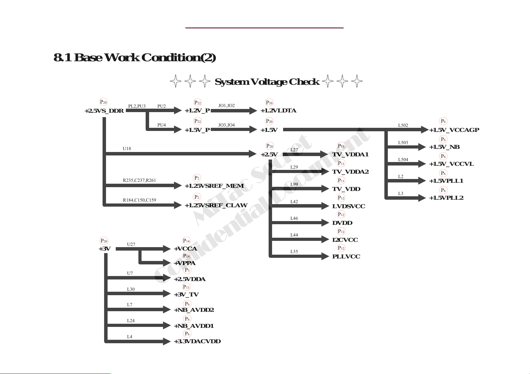
8399
8399
8.1 Base Work Condition(2)
N/B Maintenance
N/B Maintenance
System Voltage Check
P20
+2.5VS_DDR
P20
+3V
PL2,PU3
U18
R235,C237,R261
R184,C150,C159
U27
U7
L30
L7
L24
L4
PU2
PU4
P22
JO1,JO2
+1.2V_P
P22
JO3,JO4
+1.5V_P
P2
+1.25VSREF_MEM
P2
+1.25VSREF_CLAW
MiTac Secret
P14
+VCCA
P14
P20
+1.2VLDTA
P20
+1.5V
P20 P11
+2.5V
L27
L29
L99
L42
L46
L44
L35
TV_VDDA1
P11
TV_VDDA2
P11
TV_VDD
P12
LVDSVCC
P12
DVDD
P12
I2CVCC
P12
PLLVCC
L502
L503
L504
L2
L3
+VPPA
P3
+2.5VDDA
Confidential Document
P11
+3V_TV
P6
+NB_AVDD2
P6
+NB_AVDD1
P6
+3.3VDACVDD
P6
+1.5V_VCCAGP
P6
+1.5V_NB
P6
+1.5V_VCCVL
P6
+1.5VPLL1
P6
+1.5VPLL2
97
Page 99
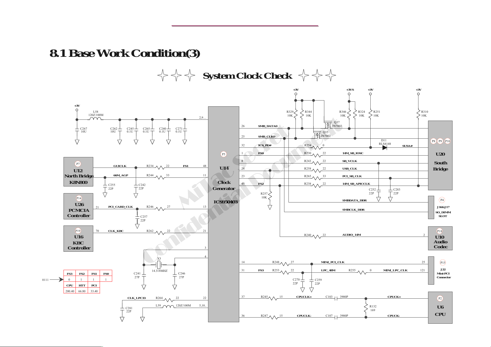
8399
8399
8.1 Base Work Condition(3)
N/B Maintenance
N/B Maintenance
System Clock Check
0111
+3V
C267
10U
P7
U12
North Bridge
K8N800
P14
U26
PCMCIA
Controller
P19
U16
KBC
Controller
FS2 FS1 FS0
FS3
HTT PCI
CPU
66.80 33.40
200.40
L58
120Z/100M
21
11
C262
10U
GUICLK R234 22 FS1 48
66M_AGP
C255
22P
PCI_CARD_CLK
0.1U
0.1U
R244 33 11
C242
22P
R246 27 13
C257
22P
R262 22CLK_KBC70
X3
0.1U
0.1U
MiTac Secret
C271
C240
C265
C245
Confidential Document
C241
10
C281
22P
14.318MHZ
27P
R264 22CLK_LPC33 22
L59 120Z/100M 5,10..
C246
27P
2,9…
21
Generator
ICS950403
3
4
P5
U14
Clock
R324
10K
+3V
C252
22P
R132
169
R251
10K
D11
RLS4148
C283
22P
CPUCK+
CPUCK-
+3V
SUSA#
121
+3V
10K
C270
22P
CPUCLK+R245 1537
CPUCLK-
R344
10K
2N7002
R254 0
R243 228
R258 2228
R265 3323
R238 22FS245
R240 22
C259
22P
Q35
C103 3900P
C107 3900P
R329
26
SMB_DATA0
25
SMB_CLK0
32 ICS_PD#
1 R230 22 14M_SB_IOSCFS0
R257
10K
14 R248 27 MINI_PCI_CLK 25
31 R253 22 LPC_48MFS3 R255 0 MINI_LPC_CLK
R247 1536
R346
10K
Q37
2N7002
SB_VCLK
USB_CLK
PCI_SB_CLK
14M_SB_APICCLK
SMBDATA_DDR
SMBCLK_DDR
AUDIO_14M
+3VS
R310
10K
2
P8
P9
U20
South
Bridge
P4
J16&J17
SO_DIMM
SLOT
P18
U10
Audio
Codec
P15
J22
Mini-PCI
Connector
P2
U6
CPU
P10
98
Page 100
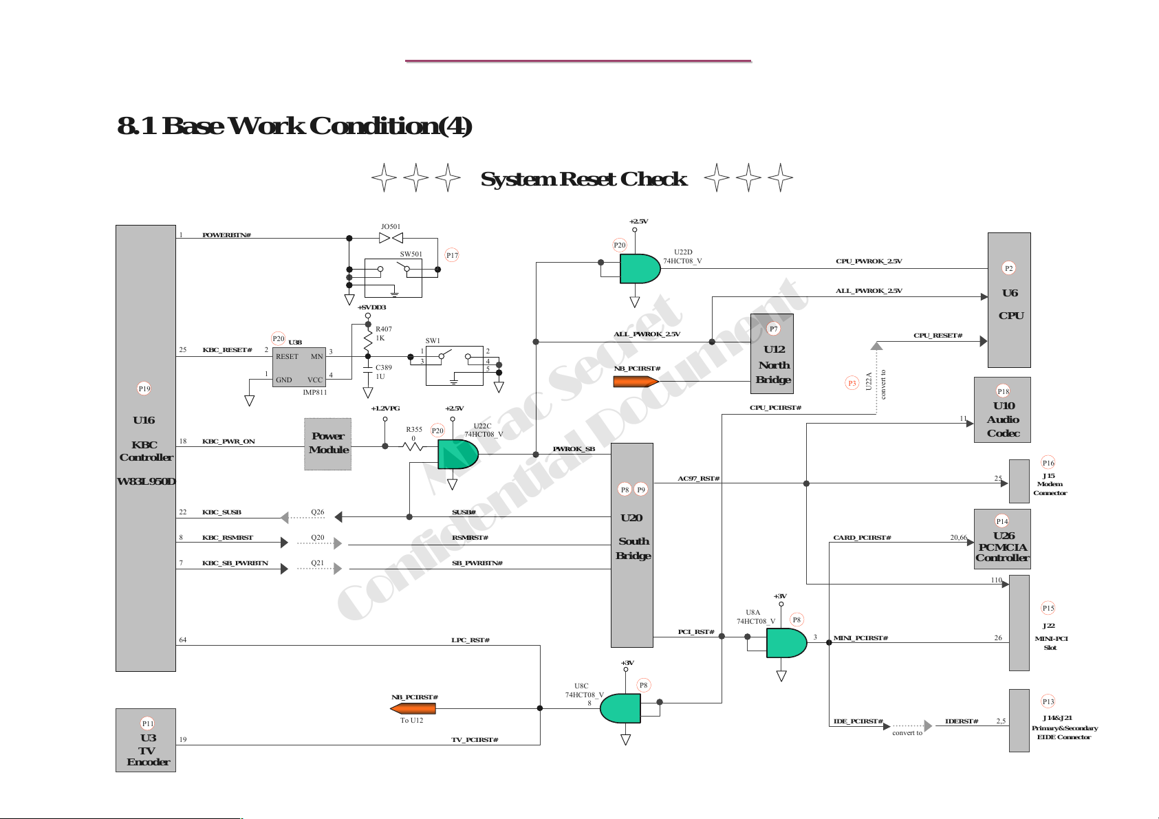
8399
8399
8.1 Base Work Condition(4)
N/B Maintenance
N/B Maintenance
System Reset Check
P19
U16
KBC
Controller
W83L950D
P11
U3
TV
Encoder
P20
ALL_PWROK_2.5V
NB_PCIRST#
South
Bridge
8
+2.5V
P8
U20
+3V
P9
P8
U22D
74HCT08_V
AC97_RST#
PCI_RST#
U12
North
Bridge
CPU_PCIRST#
U8A
74HCT08_V
CPU_PWROK_2.5V
ALL_PWROK_2.5V
P2
U6
CPU
P7
P3
U22A
convert to
CPU_RESET#
P18
U10
11
Audio
Codec
P16
J15
Modem
Connector
P15
J22
MINI-PCI
Slot
P13
J14&J21
Primary&Secondary
EIDE Connector
+3V
CARD_PCIRST# 20,66
P8
3
MINI_PCIRST#
IDE_PCIRST# IDERST# 2,5
convert to
25
P14
U26
PCMCIA
Controller
110
26
+SVDD3
+1.2VPG
JO501
R407
1K
C389
1U
SW501
R355
0
P17
SW1
1
3
P20
+2.5V
2
4
5
U22C
74HCT08_V
PWROK_SB
POWERBTN#1
P20
KBC_RESET# 225
KBC_PWR_ON18
U38
3
MNRESET
1
VCCGND
IMP811
4
Power
Module
MiTac Secret
Q26KBC_SUSB22
KBC_RSMRST RSMRST#8
KBC_SB_PWRBTN7
Q20
Q21
SUSB#
SB_PWRBTN#
Confidential Document
64
NB_PCIRST#
To U12
19
LPC_RST#
TV_PCIRST#
U8C
74HCT08_V
99
 Loading...