

MiTAC E-8590 Service Manual
SERVICE MANUAL FOR
SERVICE MANUAL FOR
SERVICE MANUAL FOR
E
E
----
8590
EE
E
E
EE
E
E----8590
EE
8590
85908590
----
8590
8590
85908590
8590
85908590
BY:
TESTING TECHNOLOGY DEPARTMENT / TSSC
TESTING TECHNOLOGY DEPARTMENT / TSSC
Jan . 2003
Dragon
Dragon

Contents
LCD PC E--
LCD PC E
8590 MAINTENANCE
8590 MAINTENANCE
1. Hardware Engineering Specification ----------------------------------------------------------------------------
1.1 Introduction ---------------------------------------------------------------------------------------------------------
1.2 System Hardware ---------------------------------------------------------------------------------------------------
1.3 TV/FM General Feature -------------------------------------------------------------------------------------------
1.4 Other Functions-----------------------------------------------------------------------------------------------------
1.5 Peripheral Components------------------------------------------------------------------------------------------------------------
1.6 Power Management-----------------------------------------------------------------------------------------------------------------
1.7 Appendix------------------------------------------------------------------------------------------------------------------------------
2. System View & Disassembly --------------------------------------------------------------------------------------
2.1 System View ---------------------------------------------------------------------------------------------------------
2.2 System Disassembly -------------------------------------------------------------------------------------------------
3. Definition & Location of Connectors / Switches Setting ----------------------------------------------------
4. Definition & Location of Major Component ------------------------------------------------------------------
5. Pin Description of Major Component ---------------------------------------------------------------------------
5.1 Pentium 4(Willamette/Northwood) mFC-PGA2 478 pins ---------------------------------------------------------
3
3
5
68
78
83
93
96
103
103
106
135
137
139
139
5.2 VIA VT8703 North Bridge with S3 Savage4 AGPX4--------------------------------------------------------------
5.3 VIA VT8235 PCI-LPC/ISA South Bridge -------------------------------------------------------------------------
6. System Block Diagram ---------------------------------------------------------------------------------------------
7. Maintenance Diagnostics ------------------------------------------------------------------------------------------
7.1 Introduction ---------------------------------------------------------------------------------------------------------
7.2 PCI Debug Card ----------------------------------------------------------------------------------------------------
145
151
160
160
161
162
1

Contents
LCD PC E--
LCD PC E
8590 MAINTENANCE
8590 MAINTENANCE
7.3 Error Codes ---------------------------------------------------------------------------------------------------------
8. Trouble Shooting ----------------------------------------------------------------------------------------------------
8.1 No Power ------------------------------------------------------------------------------------------------------------
8.2 No Display -----------------------------------------------------------------------------------------------------------
8.3 VGA Controller -----------------------------------------------------------------------------------------------------
8.4 TV Controller Error-------------------------------------------------------------------------------------------------
8.5 Memory Test Error--------------------------------------------------------------------------------------------------
8.6 Keyboard Test Error ------------------------------------------------------------------------------------------------
8.7 Hard Disk Test Error------------------------------------------------------------------------------------------------
8.8 CD-ROM Drive Test Error -----------------------------------------------------------------------------------------
8.9 USB Port Test Error-------------------------------------------------------------------------------------------------
8.10 PC Card Socket Test Error ----------------------------------------------------------------------------------------
8.11 Memory_Card Test Error -----------------------------------------------------------------------------------------
8.12 LAN Test Error ----------------------------------------------------------------------------------------------------
8.13 IEEE1394 Test Error ----------------------------------------------------------------------------------------------
8.14 Audio Driver Failure ----------------------------------------------------------------------------------------------
9. Spare Parts List ------------------------------------------------------------------------------------------------------
163
165
166
169
173
175
177
179
181
183
185
188
190
192
194
196
196
--
10. System Exploded Views--------------------------------------------------------------------------------------------
11. Circuit Diagram-----------------------------------------------------------------------------------------------------
12. Reference Material -------------------------------------------------------------------------------------------------
211
214
259
2

LCD PC E--
LCD PC E
8590 MAINTENANCE
8590 MAINTENANCE
1. Hardware Engineering Specification
1.1 Introduction
The E-Note P4N266A model motherboard would support the Desktop P4 processor (Northwood) at 2.0/2.2 GHz
and the Celeron low-profile, lidless FC-PGA2 (Flip-chip Pin Grid Array)package on socket 478.
This system is based on PCI architecture and is fully compatible with IBM PC/AT specification, which has
standard hardware peripheral interface and support Intel mobile Pentium 4-M and Desktop Pentium 4 family. The
power management complies with Advanced Configuration and Power Interface (ACPI) 1.0b. System also provides
icon LEDs to display system status, such as AC Power / Battery Power indicator and Battery charging status,
CDROM, HDD, NUM LOCK, CAP LOCK, SCROLL LOCK. It also equipped with 4 USB2.0 ports and 1 swap
module (Floppy or card reader or second HDD), one IEEE1394, one PC Card slots, LAN 10/100TX, MDC modem
and AC97 3D stereo audio functions.
The memory subsystem supports two 184pin DIMM socket for upgrading up to 1GB of DDR-SDRAM with
512Mbit DDR-SDRAM technology using PC-100 DDR-SDAM SODIMM modules with SPD. The DDR-SDRAM
controller supports standard PC2100 and PC1600 Synchronous DDR-SDRAM (Double-data-rate SDRAM) .
The VIA VT8703 /P4N266 /Twister-P4 (Apollo ProSavage DDR P4N266) North Bridge Chipset integrated with
S3 Savage4 graphics accelerator and S3’s flat panel interface into a single 664 BGA package. The Twister-P4 brings
mainstream graphics performance to the Value PC with leading-edge 2D, 3D and DVD video acceleration into a
cost effective package.
The Twister-P4 SMA(share memory architecture) system controller also provides superior performance between
the CPU, DRAM, and PCI bus with pipelined, burst, and concurrent operation.
3

LCD PC E--
LCD PC E
The 376-pin VT8233 BGA south bridge supports four levels (double words) of line buffers, type F DMA transfers
and delay transaction to allow efficient PCI bus utilization and PCI-2.1 compliant. The VT8233 also includes an
keyboard controller with PS2 mouse support , integrated DS12885 style real time clock with extended 256 byte
CMOS RAM, integrated bus master mode enhanced IDE controller with full scatter / gather capability and
extension to UltraDMA-33/66/100 for 33/66/100 MB/sec transfer rate, integrated six USB interface with root hub
and two function ports with built-in physical layer transceivers, Distributed DMA support, integrated AC-97 link for
basic audio and HSP based modem functions, integrated hardware monitoring and OnNow / ACPI compliant
advanced configuration and power management interface. VT8233 also integrates a 10/100 Mbit Fast Ethernet
Controller / MAC (Media Access Controller). The LAN controller uses an MII (Media Independent Interface)
connection to support an external 10/100 Mbit PHY for Ethernet.
The ENE CB710 CARDBUS controller supports one PCMCIA or CARDBUS interfaces.
The VIA 6306 controller supports three port multimedia feature.
8590 MAINTENANCE
8590 MAINTENANCE
To provide for the increasing number of multimedia applications, the AC97 CODEC VIA 1612A is integrated
onto the motherboard which contain 3D audio output.
A full set of software drivers and utilities are available to allow advanced operating systems such as Windows Me
and Windows 2000 and Windows XP to take full advantage of the hardware capabilities such as bus mastering IDE,
Windows 95-ready Plug & Play, Advanced Power Management (APM) and Advance configuration and power
interface (ACPI).
Following chapters will have more detail description for each individual sub-systems and functions.
4
LCD PC E--
LCD PC E
1.2 System Hardware Parts
8590 MAINTENANCE
8590 MAINTENANCE
Item
CPU
Core logic
L2 Cache
System BIOS
Memory
Video Controller
Video Memory
Clock Generator
PCMCIA
Memory Card
Reader
USB 2.0
IEEE1394
Audio System
Modem
LAN Phy
Description
Intel Desktop Pentium 4 (Northwood) mPGA478
2G,2.2G,2.26G,2.4G,2.5G,2.53G,2.6G,2.66G,2.8G
Intel Desktop Celeron mPGA478 1.7G,1.8G,1.9G
VIA VT8703A support 400MHz /533Mhz FSB + VT8235
512KB for Pentium 4 on Die
128KB for Celeron on Die
512KB Flash EPROM
Insyde -Includes System BIOS , VGA BIOS, and plug & Play capability, ACPI
-Two 184 pin DDR-DIMM socket for memory expansion
-Support PC2100 / PC1600 with SPD
Integrate S3 Savage8
Support MPEG-2 30fps, 8.5MB/s capability
1024x768 (24bit color by dithering) XGA. CMOS 18+18 bits interface
and 1600x1400 (24bit color) resolution for CRT
- Support LCD/CRT simultaneous display only
8/16/32MB share system SDRAM, default 8Mbyte
ICS 950902
REALTEK RTM360-519R
Cardbus Controller: ENE CB710
one type II slots CardBus / no ZV port support/ no wakeup at S3
Power switch: TI TPS221 or ENE CP-2211
Integrate in CB710
Support Smart Media, SD/MMC and Memory Sticker 3.3v only
USB 2.0 Controller integrate in VT8235
IEEE1394 OHCI Controller: VIA VT6306
No wakeup at S3
Not support bridge mode when system off
AC97 CODEC: Realtek ALC202
Power Amplifier: TI TPA1517 3W+3W
ASKey 56Kbps(V.90, worldwide) MDC Modem
VIA VT6103 10baseT/100 baseT – Ethernet PHY
5

LCD PC E--
LCD PC E
8590 MAINTENANCE
8590 MAINTENANCE
1.2.1 CPU-Intel Desktop Pentium4(Northwood) Processor In FC-PGA478 Package
The Intel Pentium 4 processor with 512-KB L2 cache on 0.13 micron process is a follow on to the Pentium 4
processor in the 478-pin package with Intel Net Burst. microarchitecture. The Pentium 4 processor with 512-KB L2
cache on 0.13 micron process utilizes Flip-Chip Pin Grid Array (FC-PGA2) package technology, and plugs into a
478-pin surface mount, Zero Insertion Force (ZIF) socket, referred to as the mPGA478B socket.
The Pentium 4 processor with 512-KB L2 cache on 0.13 micron process, like its predecessor, the Pentium 4
processor in the 478-pin package, is based on the same Intel 32-bit microarchitecture and maintains the tradition of
Compatibility with IA-32 software. In this document, the Pentium 4 processor with 512-KB L2 cache on 0.13 micron
process will be referred to as the “Pentium 4 processor with 512-KB L2 cache on 0.13 micron process,” or simply
“the processor.”
The Intel NetBurst microarchitecture features include hyper pipelined technology, a rapid execution engine, a 400MHz or a 533-MHz system bus, and an execution trace cache. The hyper pipelined technology doubles the pipeline
depth in the Pentium 4 processor with 512-KB L2 cache on 0.13 micron process, allowing the processor to reach
much higher core frequencies. The rapid execution engine allows the two integer ALUs in the processor to run at
twice the core frequency, which allows many integer instructions to execute in 1/2 clock tick. The 400-MHz or 533MHz system bus is a quad-pumped bus running off a 100-MHz or a 133-MHz system clock making 3.2 Gbytes/sec
and 4.3 Gbytes/sec data transfer rates possible. The execution trace cache is a first-level cache that stores
approximately 12-k decoded micro-operations, which removes the instruction decoding logic from the main
execution path, thereby increasing performance. Additional features within the Intel NetBurst microarchitecture
include advanced dynamic execution, advanced transfer cache, enhanced floating point and multi-media unit, and
Streaming SIMD Extensions 2 (SSE2). The advanced dynamic execution improves speculative execution and branch
prediction internal to the processor. The advanced transfer cache is a 512 KB, on-die level 2 (L2) cache.
6

LCD PC E--
LCD PC E
A new floating point and multi media unit has been implemented which provides superior performance for multimedia and mathematically intensive applications. Finally, SSE2 adds 144 new instructions for double-precision
floating point, SIMD integer, and memory management. Power management capabilities such as AutoHALT, StopGrant, Sleep, and Deep Sleep have been retained. The Streaming SIMD Extensions 2 (SSE2) enable break-through
levels of performance in multimedia applications including 3-D graphics, video decoding/encoding, and speech
recognition. The new packed double-precision floating-point instructions enhance performance for applications that
require greater range and precision, including scientific and engineering applications and advanced 3-D geometry
techniques, such as ray tracing.
The Pentium 4 processor with 512-KB L2 cache on 0.13 micron process Intel Net Burst microarchitecture system
bus utilizes a split-transaction, deferred reply protocol like the Pentium 4 processor. This system bus is not
compatible with the P6 processor family bus. The Intel Net Burst microarchitecture system bus uses SourceSynchronous Transfer (SST) of address and data to improve performance by transferring data four times per bus
clock (4X data transfer rate, as in AGP 4X). Along with the 4X data bus, the address bus can deliver addresses two
times per bus clock and is referred to as a “double-clocked” or 2X address bus. Working together, the 4X data bus
8590 MAINTENANCE
8590 MAINTENANCE
and 2X address bus provide a data bus bandwidth of up to 4.3 G byte s/second.
Intel will enable support components for the Pentium 4 processor with 512-KB L2 cache on 0.13 micron process
including heat sinks, heat sink retention mechanisms, and sockets. Manufacturability is a high priority; hence,
mechanical assembly can be completed from the top of the motherboard and should not require any special tooling.
The processor system bus uses a variant of GTL+signalling technology called Assisted Gunning Transceiver Logic
(AGTL+) signal technology.
7

LCD PC E--
LCD PC E
8590 MAINTENANCE
8590 MAINTENANCE
1.2.1.1 Intel Desktop Pentium 4 Processor (Northwood) Microarchitecture Summary
The following features summarize the Intel Pentium 4 Processor microarchitecture:
Available at 2 GHz, 2.20 GHz, 2.26 GHz,2.40 GHz, and 2.53 GHz
Binary compatible with applications running on previous members of the Intel microprocessor line
Intel® Net Burst™ micro-architecture
System bus frequency at 400 MHz and 533 MHz
Rapid Execution Engine: Arithmetic Logic Units (ALUs) run at twice the processor core frequency
Hyper Pipelined Technology
Advance Dynamic Execution
----Very deep out-of-order execution
----Enhanced branch prediction
Level 1 Execution Trace Cache stores 12K micro-ops and removes decoder latency from main execution loops
8 KB Level 1 data cache
512 KB Advanced Transfer Cache (on- die, full speed Level 2 (L2) cache) with 8-way associativity and Error
Correcting Code (ECC)
144 Streaming SIMD Extensions 2 (SSE2) instructions
Enhanced floating point and multimedia unit for enhanced video, audio, encryption, and 3D performance
8
LCD PC E--
LCD PC E
Power Management capabilities
----System Management mode
----Multiple low-power states
Optimized for 32-bit applications running on advanced 32-bit operating systems
8-way cache associativity provides improved cache hit rate on load/store operations.
8590 MAINTENANCE
8590 MAINTENANCE
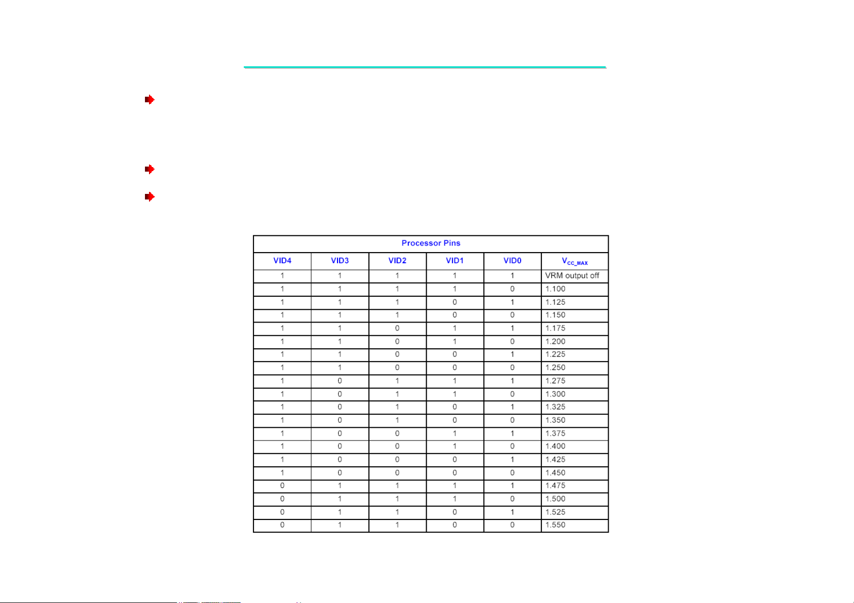
Table 1.Voltage identification Definition for Desktop Northwood
9

LCD PC E--
LCD PC E
8590 MAINTENANCE
8590 MAINTENANCE
1.2.2 CPU – Intel Celeron Processor In Micro-PGA 478 Package
The Intel® Celeron® processor in the 478-pin package utilizes Flip-Chip Pin Grid Array (FC-PGA2) package
technology, and plugs into a 478-pin surface mount, Zero Insertion Force (ZIF) socket, referred to as the
mPGA478B socket. The Celeron processor in the 478-pin package maintains the tradition of compatibility with IA32 software. The Celeron processor in the 478-pin package is designed for uni-processor based Value PC desktop
systems. Features of processor include hyper pipelined technology, a 400 MHz system bus, and an execution trace
cache. The 400 MHz system bus is a quad-pumped bus that is clocked with a 100 MHz system clock, making 3.2
GB/sec data transfer rates possible. The execution trace cache is a first level cache that stores approximately 12k
decoded micro-operations, which removes the decoder from the main execution path. Additional features include
advanced dynamic execution, advanced transfer cache, enhanced floating point and multi-media unit, and Streaming
SIMD Extensions 2 (SSE2). The advanced dynamic execution improves speculative execution and branch prediction
internal to the processor. The advanced transfer cache is a 128 KB, on-die level 2 (L2) cache. The floating point and
multimedia units have 128 bit wide registers with a separate register for data movement. Finally, SSE2 support
includes instructions for double-precision floating point, SIMD integer, and memory management. Power
management capabilities such as AutoHALT, Stop-Grant, Sleep, and Deep Sleep have also been retained. The
Celeron processor in the 478-pin package 400 MHz system bus utilizes a split-transaction, deferred reply protocol.
This system bus is not compatible with the P6 processor family bus. The 400 MHz system bus uses SourceSynchronous Transfer (SST) of address and data to improve throughput by transferring data four times per bus clock
(4X data transfer rate, as in AGP 4X). Along with the 4X data bus, the address bus can deliver addresses two times
per bus clock, and is referred to as a “double-clocked” or 2X address bus. Working together, the 4X data bus and 2X
address bus provide a data bus bandwidth of up to 3.2 GB/second. Intel will be enabling support components for the
Celeron processor in the 478-pin package including a heatsink, heat sink retention mechanism, and socket.
Manufacturability is a high priority; hence mechanical assembly can be completed from the top of the motherboard
and should not require any special tooling. The processor system bus uses a variant of GTL+ signaling technology
called Assisted Gunning Transceiver Logic (AGTL+) signalling technology.
10

LCD PC E--
LCD PC E
8590 MAINTENANCE
8590 MAINTENANCE
1.2.2.1 Intel Celeron–Processor Microarchitecture Summary
The following features summarize the Intel Celeron Processor Microarchitecture:
Available at 1.70,1.8G and 1.90 GHz
Binary compatible with applications running on previous members of the Intel microprocessor line
System bus frequency at 400 MHz.
Rapid Execution Engine: Arithmetic Logic Units (ALUs) run at twice the processor core frequency.
Hyper Pipelined Technology.
Advanced Dynamic Execution
----Very deep out-of-order execution
----Enhanced branch prediction
8 KB Level 1 data cache
Level 1 Execution Trace Cache stores 12K micro-ops and removes decoder latency from main execution loops
128 KB Advanced Transfer Cache (on-die,full speed Level 2 (L2) cache) with Error Correction Code (ECC)
144 Streaming SIMD Extensions 2 (SSE2) Instructions
Power Management capabilities
----System Management mode
----Multiple low-power states
Optimized for 32-bit applications running on advanced 32-bit operating systems
11
LCD PC E--
LCD PC E
8590 MAINTENANCE
8590 MAINTENANCE
1.2.3 VIA VT8703 (P4N266 Twister P4) North Bridge with S3 ProSavage 8 AGPx4
The ProSavageDDR P4N266 (VT8703 “Twister P4” North Bridge plus VT8233 South Bridge) is a high
performance, cost-effective and energy efficient SMA chip set for the implementation of mobile personal computer
systems with 400 MHz (100 MHz QDR) CPU host bus (“Front Side Bus”) based on 64-bit Intel Pentium-4 superscalar processors. This data sheet describes the VT8703 North Bridge portion of the P4N266 chipset (except for
detailed register descriptions for the integrated graphics controller which are described in a separate document
published by S3 Graphics). The VT8235 South Bridge is described in a separate data sheet.
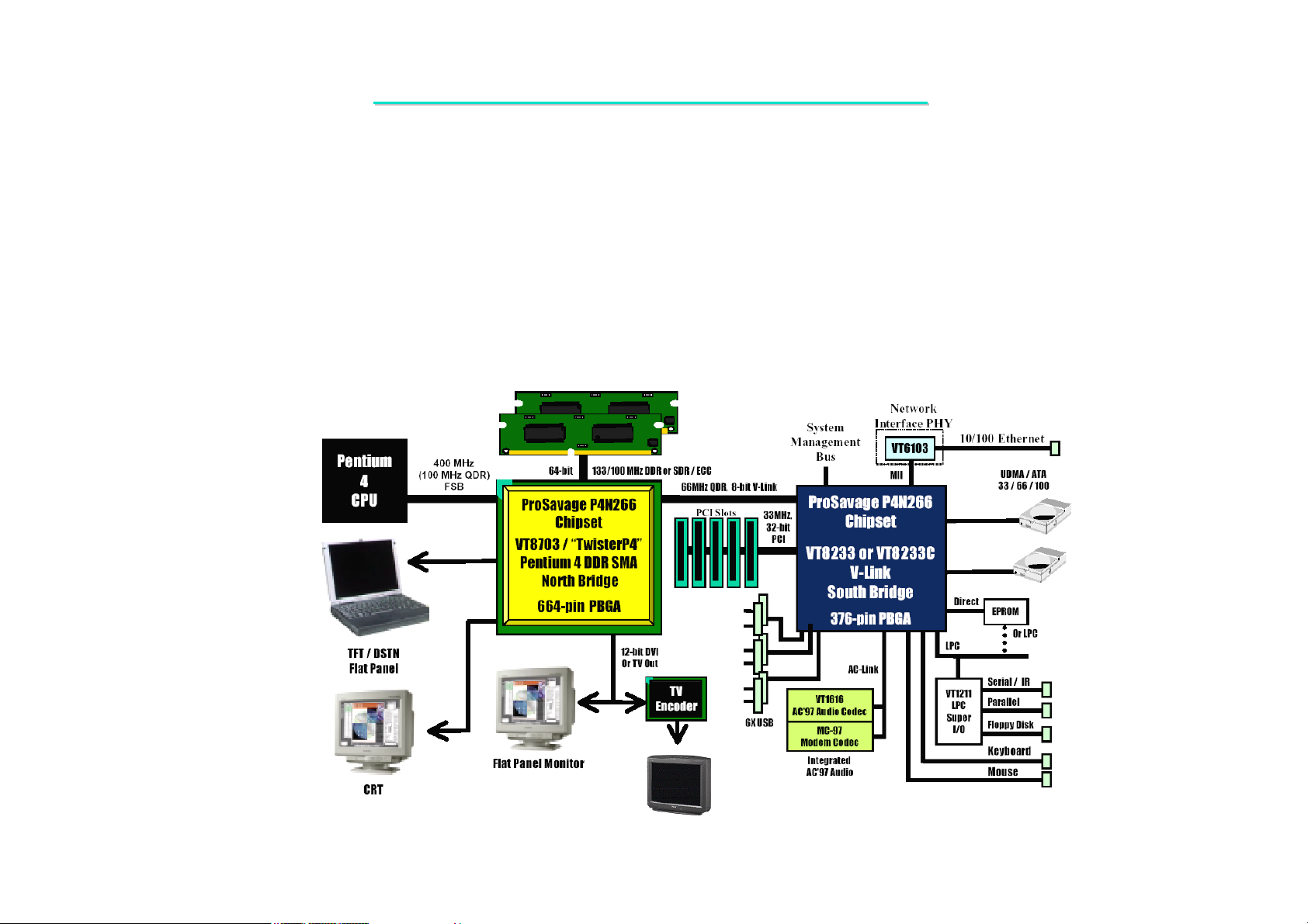
Figure . ProSavageDDR P4N266 Chipset System Block Diagram
12

LCD PC E--
LCD PC E
The P4N266 chip set consists of the VT8703 North Bridge (664 pin BGA) and the VT8233 V-Link South Bridge
(376 pin BGA). The VT8703 (which may also be referred to as a “Host System Controller”) integrates VIA’s
VT8653 Apollo Pro266T system controller with CPU bus extensions to support Pentium 4, S3 Graphics’ Savage4
2D/3D graphics accelerator and S3 Graphics’ flat panel monitor and TV out interfaces into a single 664 BGA
package. The VT8703 provides superior performance between the CPU, DRAM, V-Link bus and internal or external
AGP 4x graphics controller bus with pipelined, burst, and concurrent operation. The VT8233 (which also may be
referred to as a “V-Link Client Controller”) is a highly integrated PCI / LPC controller. Its internal bus structure is
based on a 66 MHz PCI bus that provides 2x bandwidth compared to previous generation PCI bridge chips. The
VT8233 also provides a 266MB/sec bandwidth Host/Client V-Link interface with V-Link-PCI and V-Link-LPC
controllers. It supports five PCI slots of arbitration and decoding for all integrated functions and LPC bus.
The VT8703 supports eight banks of SDR / DDR SDRAMs up to 4 GB. The DRAM controller supports PC2100 /
PC1600 Double-Data-Rated (DDR) SDRAM but can also support standard PC133 / PC100 Synchronous DRAM
(SDR SDRAM). The DDR / SDR DRAM interface allows zero wait state bursting between the DRAM and the data
8590 MAINTENANCE
8590 MAINTENANCE
buffers at 100 / 133 MHz. The different banks of DRAM can be composed of an arbitrary mixture of 1M / 2M / 4M /
8M / 16M / 32M / 64M x 8/16/32 DRAMs. The DRAM controller also supports optional ECC (single-bit error
correction and multi-bit detection) or EC (error checking) capability. The DRAM controller can run either
synchronous or pseudo-synchronous with the host CPU bus.
The VT8703 host system controller supports a high speed 8-bit 66 MHz Quad Data Transfer interconnect (V-Link)
to the VT8233 South Bridge. The chip also contains a built-in bus-to-bus bridge to allow simultaneous concurrent
operations on each bus. Five levels (double words) of post write buffers are included to allow for concurrent CPU and
V-Link operation. For V-Link Host operation, forty-eight levels (double words) of post write buffers and sixteen
levels (double words) of prefetch buffers are included for concurrent V-Link bus and DRAM/cache accesses. When
combined the V-Link Host / Client controllers, it realizes a complete PCI sub-system and supports enhanced PCI bus
commands such as Memory-Read-Line, Memory-Read-Multiple and Memory- Write-Invalid commands to minimize
13

LCD PC E--
LCD PC E
snoop overhead. In addition, advanced features are supported such as snoop ahead, snoop filtering, L1 write-back
forward to PCI master, and L1 write-back merged with PCI post write buffers to minimize PCI master read latency
and DRAM utilization. Delay transaction and read caching mechanisms are also implemented for further
improvement of overall system performance.
The P4N266 North Bridge also integrates S3 Graphics’ Savage4 graphics accelerator into a single chip. The
P4N266 brings mainstream graphics performance to the Value PC with leading-edge 2D, 3D and DVD video
acceleration into a cost effective package. Based on its capabilities, the P4N266 is an ideal solution for the consumer,
corporate mobile users and entry level professionals.
The industry’s first integrated Pentium 4 AGP 4x solution to support DDR memory, the P4N266 combines AGP
4x performance with Microsoft DirectX texture compression and massive 2Kx2K textures to deliver unprecedented
3D performance and image quality for the Value PC mobile market. For sophisticated power management, the
VT8703 provides independent clock stop control for the CPU / SDRAM and AGP bus plus Dynamic CKE control
for powering down of the SDRAM. A separate suspend-well plane is implemented for the SDRAM control signals
8590 MAINTENANCE
8590 MAINTENANCE
for Suspend-to-DRAM operation. Coupled with the VT8233 south bridge chip, a complete power conscious PC
main board can be implemented with no external TTLs.
High-Performance 3D Accelerator
Featuring a new super-pipelined 128-bit engine, the P4N266 chipset utilizes a single cycle architecture that
provides high performance along with superior image quality. Several new features enhance the 3D architecture,
including single-pass multitexturing, anisotropic filtering, and an 8-bit stencil buffer. The P4N266 also offers the
industry’s only simultaneous usage of single-pass multitexturing and single-cycle trilinear filtering – enabling
stunning image quality without performance loss. The P4N266 further enhances image quality with true 32-bit color
rendering throughout the 3D pipeline to produce more vivid and realistic images. The P4N266’s advanced triangle
14

LCD PC E--
LCD PC E
setup engine provides industry leading 3D performance for a realistic user experience in games and other
interactive 3D applications. The 3D engine is optimized for AGP texturing from system memory.
128-bit 2D Graphics Engine
The P4N266’s advanced 128-bit 2D graphics engine delivers high-speed 2D acceleration for productivity
applications. Several enhancements have been made to the 2D architecture to optimize SMA performance and to
provide acceleration in all color depths.
DVD Playback and Video Conferencing
The P4N266 provides the ideal architecture for high quality MPEG-2 based DVD applications and video
conferencing. For DVD playback, the P4N266’s video accelerator offloads the CPU by performing the planar to
packed format conversion and motion compensation tasks, while its enhanced scaling algorithm delivers incredible
8590 MAINTENANCE
8590 MAINTENANCE
full-screen video playback. For video conferencing, P4N266’s multiple video windows enable a cost effective
solution.
LCD, Flat Panel Monitor, and TV Out Support
The P4N266 supports a wide variety of DSTN or TFT panels through a 36-bit interface. This includes support for
VGA, SVGA, XGA, SXGA+, UXGA, and UXGA+ TFT color panels with 9-bit, 12-bit, 18-bit (both 1 pixel/clock
and 2 pixels/clock), 24-bit and 36-bit interfaces. Enhanced STN hardware with 256 gray scale support and advanced
frame rate control to provide up to 16.7 million colors. All resolutions are supported up to 1280x1024. In addition,
the panel interface can be configured to connect to external LVDS transmitters to support 18-bit, 24-bit, or 2x18-bit
TFT single-channel or dual channel LVDS panels.
15
LCD PC E--
LCD PC E
8590 MAINTENANCE
8590 MAINTENANCE
An alternative to the 36-bit panel interface is a 12-bit interface to external TMDS encoders. This interface is Digital
Visual Interface (DVI) 1.0 compliant. This interface can alternatively be configured to drive an external TV encoder
chip for display output to a standard television set.
High Screen Resolution CRT Support
System Memory
Frame Buffer Size
16/32MB8MBResolutions
Supported
√√640x480/16/32
√√800x600/16/32
√√1024x768/16/32
√√1280x1024x8
Table . Supported CRT screen Resolutions
√√1280x1024x16
√√1280x1024x32
√√1620x1200x8
√√1620x1200x16
√√1620x1200x32
√√1920x1440x8
√√1920x1440x16
16
LCD PC E--
LCD PC E
8590 MAINTENANCE
8590 MAINTENANCE
LCD and CRT Screen Resolution Support (1)
CRT Refresh
2
Reso lu tion
320x200
320x240
400x300
512x384
640x400
640x480
720x480
720x576
Bpp
Vesa Mode
8 13
16 10E
32 10F
8 131
16 133
32 134
8 141
16 143
32 144
8 151
16 153
32 154
8 100
16
11D
32 11E
8 101
16 111
32 112
8 171
16 173
32 175
8 17C
16 17E
32 17F
LCD XGA
LCD SXGA**
LCD SXGA+
LCD UXGA**
CE CE CE CE
CE CE CE CE
CE CE CE CE
CE CE CE CE
CE CE CE CE
CE CE CE CE
CE CE CE CE
CE CE CE CE
CE CE CE CE
CE CE CE CE
CE CE CE CE
CE CE CE CE
CE CE CE CE
CE CE CE CE
CE CE CE CE
CE CE CE CE
CE CE CE CE
CE CE CE CE
C C C C
C C C C
C C C C
C C C C
C C C C
C C C C
60
√
70
72
75
85
√
√
100
√
√
√
√
√
√
√
√
√
√
√
√
√
√
√
√ √ √
√ √ √
√ √ √
√
√
√
√
√
√
√ √
ME, W2k 2D
√
√
√
√
√
√
√
√
√
√
√
√
√
√
√
D/OGL
DOS
√
√
√
√
√
√
√
√
√
√
√
√
√
√
√
√ √ √ √
√ √ √ √
√ √ √ √
4
√ √
√ √
√ √
√ √
√ √
√
4
√
4
√
4
√
4
√
4
√
Basic OS
LCD PC E--
LCD PC E
8590 MAINTENANCE
8590 MAINTENANCE
LCD and CRT Screen Resolution Support (2)
CRT Refresh
Resolution
1024x768
1280x1024
1400x1050
1600x1200
** Evaluation performed on CRT until panel availability
Not supported at any refresh rate
Supported with 8 MB, or higher video memory for Logo’d drivers
√
133Mhz Mclk Required for overlay
1
2 Overlay not supported
133Mhz Mclk Required for Mode and Overlay not supported
3
4 720 Desktop modes on NT4, Win2K and Whistler, not supported on Win9x,ME
Bpp
Vesa Mode
8 105
16 117
32 118
8 107
16 11A
32 11B
8 13B
16 13C
32 13E
8 120
16 122
LCD XGA
LCD SXGA**
LCD SXGA+
LCD UXGA**
F CE CE CE
F CE CE CE
CE 1 CE 1 CE 1
F 1
P F CE CE
P F CE CE
P 3 F 3
P P F CE
P P F CE
P 3 P 3 F 3
P 1 P 1 P 1 F1
P 2 P 2 P 2 F 2
CE 3 CE 3
CE 3
0
60
√ √
√ √
√1 √1
√
√
√3
√
√
√3
√1
√2
2
75
√ √
√ √
√2 √3
√
√2
√3
√
√2
100
85
DOS
√ √ √ √
√ √ √ √
√ √ √ √
√ √ √ √
√ √ √ √
√ √ √ √
√ √ √ √
√ √ √ √
√ √ √ √
√ √ √ √
√ √ √ √
D/OGL
ME, W2k 2D
2
Basic OS
Table 2: CRT and LCD screen resolution support.
18

LCD PC E--
LCD PC E
Defines Integrated Solutions for Mobile PC Designs
High performance SMA VT8703 North Bridge: Integrated Pentium 4 VIA DDR North Bridge and S3 Graphics
Savage4 2D/3D AGP 4x Graphics Controller in a single chip
64-bit Advanced ECC Memory controller supporting PC2100/PC1600 DDR and PC100/PC133 SDR SDRAM
Combines with VIA VT8233 V-Link South Bridge for integrated LAN, Audio, ATA100 IDE, and 6 USB ports
2.5V Core and AGTL+ I/O
37.5 x 37.5mm PBGA package with 664 balls
High Performance CPU Interface
Support for Intel™ Pentium 4 processors with 400 MHz (100 MHz QDR) CPU Front Side Bus (FSB)
8590 MAINTENANCE
8590 MAINTENANCE
Built-in Phase Lock Loop circuitry for optimal skew control within and between clocking regions
Nine outstanding transactions (eight In-Order Queue (IOQ) plus one output latch)
Dynamic deferred transaction support
High Bandwidth 266MB/S 8-bit V-Link Host Controller
Supports 66MHz V-Link Host interface with peak bandwidth of 266MB/S
Operates at 2X or 4X modes
Full duplex commands with separate command / strobe
19

LCD PC E--
LCD PC E
Request / Data split transaction
Configurable outstanding transaction queue for Host to V-Link Client accesses
Supports Defer / Defer-Reply transactions
Transaction assurance for V-Link Host to Client access eliminates V-Link Host-Client Retry cycles
Intelligent V-Link transaction protocol to eliminate data wait-state / throttle transfer latency
All V-Link transactions for both Host and Client have a consistent view of transaction data depth and buffer size
to avoid data overflow
Highly efficient V-Link arbitration with minimum overhead
All V-Link transactions have predictable cycle length with known command / data duration
8590 MAINTENANCE
8590 MAINTENANCE
Advanced High-Performance DDR /SDR DRAM Controller
DRAM interface pseudo-synchronous with host CPU (100 MHz) for most flexible configuration
DRAM interface may be faster than CPU by 33 MHz to allow use of 133 MHz memory with 100 MHz FSB clock
Concurrent CPU, AGP, and V-Link access
Supports SDR and DDR SDRAM memory types
Clock Enable (CKE) control for SDRAM power reduction in high speed systems
Mixed 16M / 32M / 64M x 8/16/32 DRAMs
Supports 8 banks up to 4 GB DRAMs (512Mb x8/x16 DRAM technology )
20

LCD PC E--
LCD PC E
Flexible row and column addresses. 64-bit data width only
LVTTL 3.3V DRAM interface with 5V-tolerant inputs for SDR SDRAM and 2.5V SSTL-2 DRAM interface
for DDR SDRAM
Programmable I/O drive capability for MA, MD, and command signals
Dual copies of MA and control signals for improved drive
Optional ECC (single-bit error correction and multi-bit error detection ) or EC (error checking only) for DRAM
integrity
Two-bank interleaving for 16Mbit SDRAM support
Two-bank and four bank interleaving for 64Mb, 128Mb, 256Mb, 512Mb SDRAM support
Supports maximum 16-bank interleave (i.e., 16 pages open simultaneously); banks are allocated based on LRU
8590 MAINTENANCE
8590 MAINTENANCE
Seamless DRAM command scheduling for maximum DRAM bus utilization
- (e.g., precharge other banks while accessing the current bank)
Four cache lines (16 quad words) of CPU to DRAM write buffers
Four cache lines of CPU to DRAM read prefetch buffers
Read around write capability for non-stalled CPU read
Speculative DRAM read before snoop result
Burst read and write operation
Burst length 4 and 8 for SDR and DDR
21

LCD PC E--
LCD PC E
Supports DDR SDRAM CL 2/2.5/3 and 1T per command
1T and 2T command rate for SDR and DDR which can be specified bank by bank
Decoupled and burst DRAM refresh with staggered RAS timing (CAS before RAS or self refresh )
Full Featured Internal Accelerated Graphics Port (AGP) Controller
Supports 266 MHz 4x and 133 MHz 2x transfer modes for AD and SBA signaling
AGP specification v2.0 compliant
Pseudo-synchronous with the host CPU bus with optimal skew control
Gle-pass multiple textures
Supports SideBand Addressing (SBA) mode (non-multiplexed address / data)
8590 MAINTENANCE
8590 MAINTENANCE
AGP pipelined split-transaction long-burst transfers up to 1GB/sec
Eight level read request queue
Four level posted-write request queue
Thirty-two level (quadwords) read data FIFO (256 bytes)
Sixteen level (quadwords) write data FIFO (128 bytes)
Intelligent request reordering for maximum AGP bus utilization
Supports Flush/Fence commands
Graphics Address Relocation Table (GART)
22

LCD PC E--
LCD PC E
- One level TLB structure
- Sixteen entry fully associative page table
- LRU replacement scheme
- Independent GART lookup control for host / AGP / PCI master accesses
Windows 95 OSR-2 VXD and integrated Windows 98 / Windows 2000 miniport driver support
Extensive LCD Support
36-bit DSTN/TFT flat panel interface with 256 gray shade support
Support for external LVDS transmitters for interface to LVDS panels
- 18-bit or 24-bit single-channel LVDS transmitters for up to SXGA resolution (1280x1024)
8590 MAINTENANCE
8590 MAINTENANCE
- 2x18-bit dual-channel LVDS transmitters for up to UXGA resolution (1600x1200)
Panel power sequencing
Hardware Suspend/Standby control
High Resolution CRT RGB Interface
250 MHz RAMDAC on chip with Gamma Correction
Horizontal / Vertical Sync outputs compliant with Monitor Power Management protocols
I2C Serial Bus for DDC Monitor Communications
23

LCD PC E--
LCD PC E
Simultaneous display of CRT with TV, DVI Flat Panel Monitor, or TFT/DSTN/LVDS LCD panel display
Integrated Savage4 2D/3D/Video Accelerator
Optimized Shared Memory Architecture (SMA)
8 / 16 / 32 MB frame buffer using system memory
Floating point triangle setup engine
Single cycle 128-bit 3D architecture
8M triangles/second setup engine
140M pixels/second trilinear fill rate
Full internal AGP 4x performance
8590 MAINTENANCE
8590 MAINTENANCE
Microsoft DirectX texture compression
Next generation, 128-bit 2D graphics engine
High quality DVD video playback
Flat panel monitor support
2D/3D resolutions up to 1920x1440
3D Rendering Features
Single-pass multiple textures
24

LCD PC E--
LCD PC E
• Anisotropic filtering
• 8-bit stencil buffer
• 32-bit true color rendering
• Specular lighting and diffuse shading
• Alpha blending modes
• Massive 2K x 2K textures
• MPEG-2 video textures
• Vertex and table fog
• 16 or 24-bit Z-buffering
• Reflection mapping, texture morphing, shadows, procedural textures and atmospheric effects
8590 MAINTENANCE
8590 MAINTENANCE
2D Hardware Acceleration Features
ROP3 Ternary Raster Operation BitBLTs
8, 16, and 32 bpp mode acceleration
25

LCD PC E--
LCD PC E
Motion Video Architecture
High quality up/down scaler
Planar to packed format conversion
Motion compensation for full speed DVD playback
Hardware subpicture blending and highlights
Multiple video windows for video conferencing
Contrast, hue, saturation, brightness and gamma controls
Flat Panel Monitor / TV Output Support
Digital Visual Interface (DVI) 1.0 compliant for flat panel monitors
8590 MAINTENANCE
8590 MAINTENANCE
Optional configuration of DVI outputs as digital output port for external NTSC/PAL TV encoder
Full Software Support
Drivers for major operating systems and APIs: Windows∨ 9x/ME, Windows NT 4.0, Windows 2000, Windows
XP, Direct3D⇔, DirectDraw⇔ and DirectShow⇔, and OpenGL⇔ ICD for Windows 9x/ME, NT, 2000, and XP
North Bridge/Chipset and Video BIOS support
26

LCD PC E--
LCD PC E
Advanced System Power Management Support
Power down of SDRAM (CKE)
VTT suspend power plane preserves memory data
Suspend-to-DRAM and self-refresh power down
Low-leakage I/O pads
ACPI 1.0B and PCI Bus Power Management 1.1 compliant
8590 MAINTENANCE
8590 MAINTENANCE
1.2.4 VIA VT8235 BGA PCI-LPC/ISA South Bridge
The VT8235 South Bridge is a high integration, high performance, power-efficient, and high compatibility device
that supports Intel and non-Intel based processor to V-Link bus bridge functionality to make a complete Microsoft
PC2001-compliant PCI/LPC system. The VT8235 includes standard intelligent peripheral controllers:
a) IEEE 802.3 compliant 10 / 100 Mbps PCI bus master Ethernet MAC with standard MII interface to external
PHYceiver.
b) Master mode enhanced IDE controller with dual channel DMA engine and interlaced dual channel commands.
Dedicated FIFO coupled with scatter and gather master mode operation allows high performance transfers between
PCI and IDE devices. In addition to standard PIO and DMA mode operation, the VT8235 also supports the
UltraDMA-133, 100, 66, and 33 standards to allow reliable data transfer at rates up to 133 MB/sec. The IDE
controller is SFF-8038i v1.0 and Microsoft Windows-family compliant.
27

LCD PC E--
LCD PC E
c) Universal Serial Bus controller that is USB v2.0 / 1.1 and Universal HCI v2.0 / 1.1 compliant. The VT8235
includes three root hubs with six function ports with integrated physical layer transceivers. The USB controller
allows hot plug and play and isochronous peripherals to be inserted into the system with universal driver support.
The controller also implements legacy keyboard and mouse support so that legacy software can run transparently in
a non-USB-aware operating system environment.
d) Keyboard controller with PS2 mouse support.
e) Real Time Clock with 256 byte extended CMOS. In addition to the standard ISA RTC functionality, the
integrated RTC also includes the date alarm, century field, and other enhancements for compatibility with the ACPI
standard.
f) Notebook-class power management functionality compliant with ACPI and legacy APM requirements. Multiple
sleep states (power-on suspend, suspend-to-DRAM, and suspend-to-Disk) are supported with hardware automatic
wake-up. Additional functionality includes event monitoring, CPU clock throttling and stop (Intel processor
8590 MAINTENANCE
8590 MAINTENANCE
protocol), PCI bus clock stop control, modular power, clock and leakage control, hardware-based and softwarebased event handling, general purpose I/O, chip select and external SMI.
g) Full System Management Bus (SMBus) interface.
h) Integrated bus-mastering dual full-duplex direct-sound AC97-link-compatible sound system.
i) Plug and Play controller that allows complete steerability of all PCI interrupts and internal interrupts / DMA
channels to any interrupt channel. One additional steerable interrupt channel is provided to allow plug and play and
reconfigurability of onboard peripherals for Windows family compliance.
28
LCD PC E--
LCD PC E
8590 MAINTENANCE
8590 MAINTENANCE
The VT8235 also enhances the functionality of the standard ISA peripherals. The integrated interrupt controller
supports both edge and level triggered interrupts channel by channel. The integrated DMA controller supports type F
DMA in addition to standard ISA DMA modes. Compliant with the PCI-2.2 specification, the VT8235 supports
delayed transactions and remote power management so that slower ISA peripherals do not block the traffic of the
PCI bus. Special circuitry is built in to allow concurrent operation without causing dead lock even in a PCI-to-PCI
bridge environment. The chip also includes eight levels(doublewords) of line buffers from the PCI bus to the ISA
bus to further enhance overall system performance.
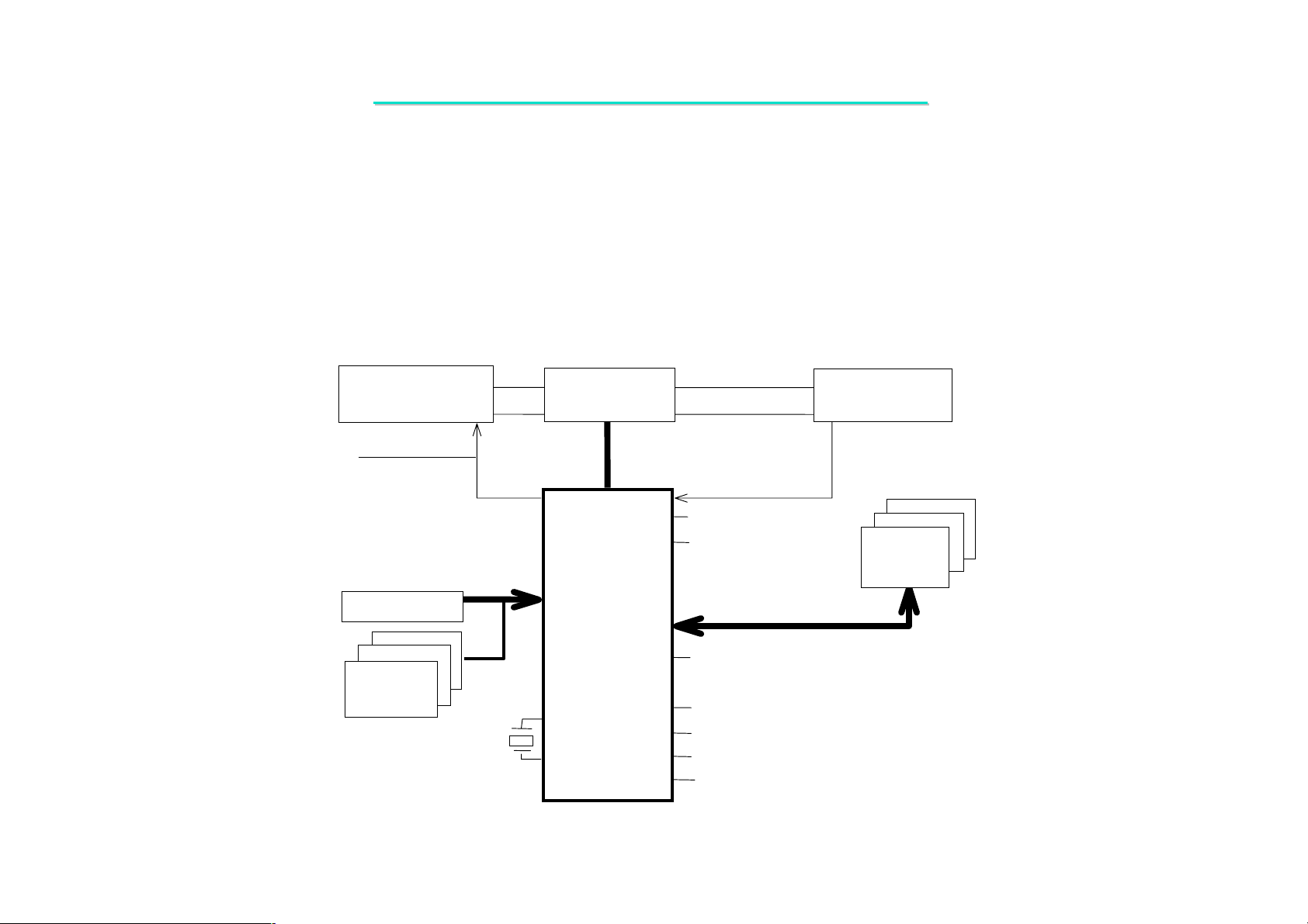
CPU/CACHE
SIDEBAND SIGNALS
Init A20M#
INTR/NMI
SMI/StopClk
FERR/IGNNE
Sleep
BOOT ROM
ONBOARD
LPCI/O
LPC
RTC
CRYSTAL
CA
CD
NORTH BRIGE
VLINK
INTERFACE
VT8235
487 BGA
MA/COMMAND
MD
SMB
USB 2.0 PORTS 0-5
KEYBOARD/MOUSE
IDE PRIM ARY AND SECONDARY
AC97LINK
APIC
GPIO, POWER CONTROL RESET
MLL FAST ETHERNER INERFACE
SYSTEM MEMORY
DIMM MODULE ID
EXPANSION
CARDS
PCI
Figure . PC System Configuration Using the VT8233
29
 Loading...