

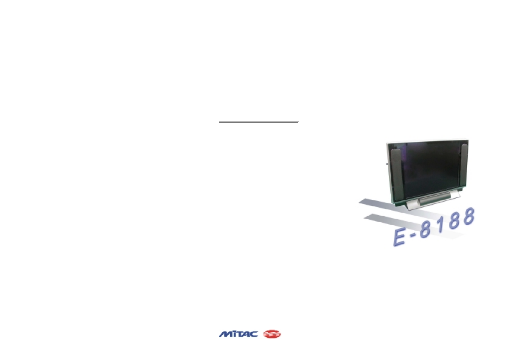
MiTAC E - 8188 Service Manual
SERVICE MANUAL FOR
SERVICE MANUAL FOR
SERVICE MANUAL FOR
E
E
E E
E
E
E E
E
E ----8188
E E
----
8188
8188
81888188
----
8188
8188
81888188
8188
81888188
BY:
TESTING TECHNOLOGY DEPARTMENT / TSSC
TESTING TECHNOLOGY DEPARTMENT / TSSC
Apr . 2003
Rain Li
Rain Li

Contents
LCD PC E--
LCD PC E
8188 MAINTENANCE
8188 MAINTENANCE
1. Hardware Engineering Specific ation ---------------------------------------------------------------------------
1.1 Introduction ---------------------------------------------------------------------------------------------------------
1.2 System Hardware ---------------------------------------------------------------------------------------------------
1.3 TV/FM General Feature -------------------------------------------------------------------------------------------
1.4 Other Functions-----------------------------------------------------------------------------------------------------
1.5 Peripheral Components------------------------------------------------------------------------------------------------------------
1.6 Power Management-----------------------------------------------------------------------------------------------------------------
1.7 Appendix------------------------------------------------------------------------------------------------------------------------------
2. System View & Disassembly -------------------------------------------- ------------------------------------------
2.1 System View ---------------------------------------------------------------------------------------------------------
2.2 System Disassembly -------------------------------------------------------------------------------------------------
3. Definition & Location of Connectors / Switches Setting ------------------------------------ ------------- ---
4. Definition & Location of Major Component --------- ---------------------------------------------------------
5. Subsystem Board Connection with System Board------------------------------------------------------------
6. Pin Description of Major Componen t ---------------------------------------------------------------------------
3
3
5
62
72
77
91
93
98
98
100
127
130
133
134
6.1 Pentium 4(Willamette/Northwood) mFC-PGA2 478 pins ---------------------------------------------------------
6.2 VIA VT8703 North Bridge with S3 Savage4 AGPX4--------------------------------------------------------------
6.3 VIA VT8235 PCI-LPC/ISA South Bridge -------------------------------------------------------------------------
7. System Block Diagram ---------------------------------------- ------------- -------------------------- ------------- -
8. Maintenance Diagnostics ------------------------------------------------------------------------------------------
134
140
145
154
155
1

Contents
LCD PC E--
LCD PC E
8188 MAINTENANCE
8188 MAINTENANCE
8.1 Introduction ---------------------------------------------------------------------------------------------------------
8.2 PCI Debug Card ----------------------------------------------------------------------------------------------------
8.3 Error Codes ---------------------------------------------------------------------------------------------------------
9. Trouble Shooting ----------------------------------------------------------------------------------------------------
9.1 No Power ------------------------------------------------------------------------------------------------------------
9.2 No Display -----------------------------------------------------------------------------------------------------------
9.3 AGP Controller Error-----------------------------------------------------------------------------------------------
9.4 Memory Test Error -------------------------------------------------------------------------------------------------
9.5 Keyboard Test Error ------------------------------------------------------------------------------------------------
9.6 Hard Disk Test Error------------------------------------------------------------------------------------------------
9.7 CD-ROM Drive Test Error------------------------------------------------------------------------------------------
9.8 USB Port Test Error ------------------------------------------------------------------------------------------------
9.9 PC Card Socket Test Error ----------------------------------------------------------------------------------------
9.10 Memory_Card Test Error -----------------------------------------------------------------------------------------
9.11 LAN Test Error -----------------------------------------------------------------------------------------------------
9.12 IEEE1394 Test Error-----------------------------------------------------------------------------------------------
9.13 Audio Driver Failure -----------------------------------------------------------------------------------------------
155
156
157
159
160
164
168
171
173
175
177
179
182
184
186
188
190
10. Spare Parts List ---------------------------------------------------------- --------------------------------------- ---
11. System Exploded Views----- ------------ --------------------------------------- ------------------------------------
12. Circuit Diagram--------------------- -------------------------------------- -------------------------- ----------------
13. Reference Material -------------------------------------------------------------------------------------------------
193
204
***
***
2

LCD PC E--
LCD PC E
8188 MAINTENANCE
8188 MAINTENANCE
1. Hardware Engineering Specification
1.1 Introduction
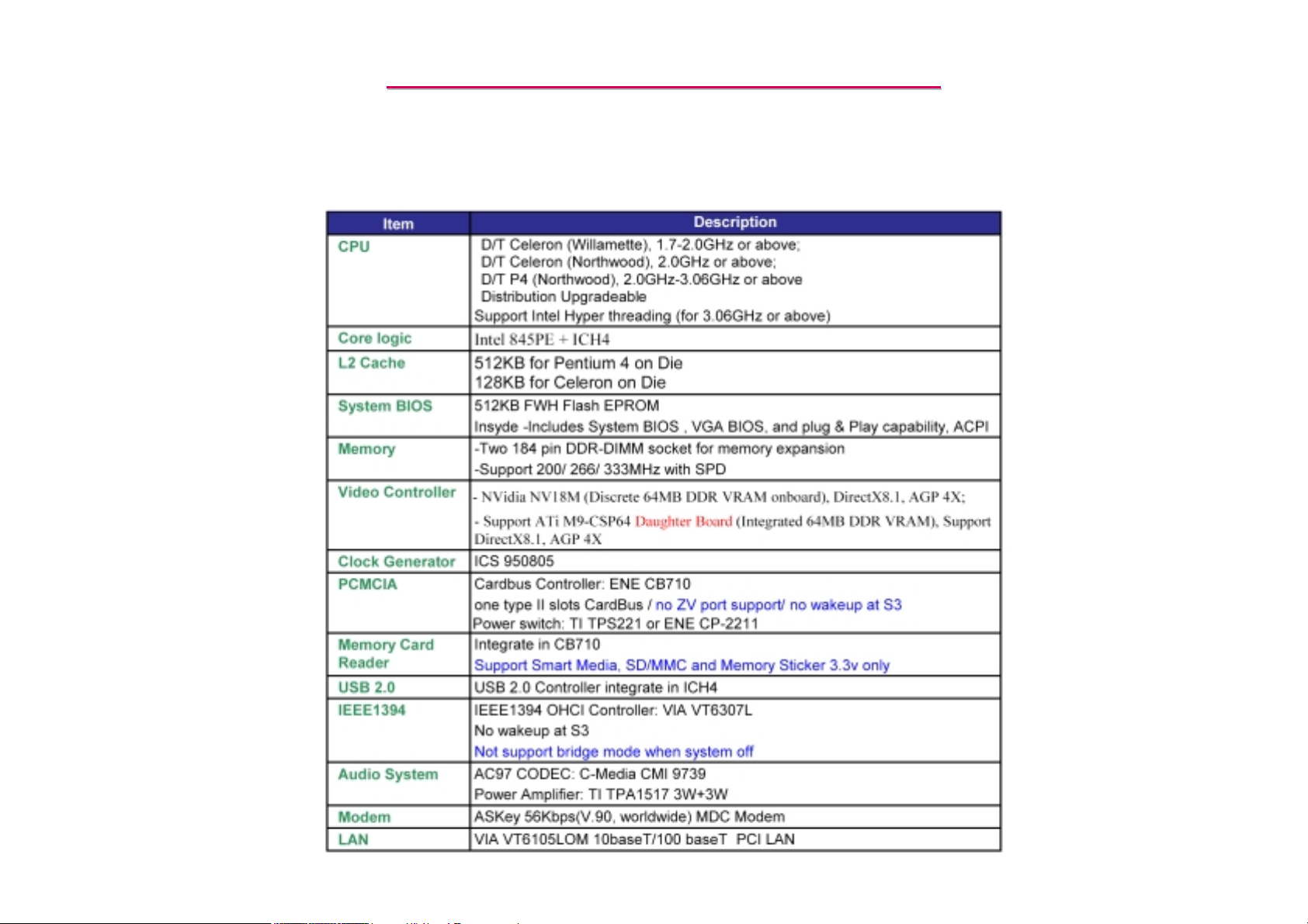
The E8188 model motherboard would support the Desktop P4 processor (Northwood) at 2.0~3.06 GHz or above
(supported Intel Hyper threading) and the Celeron low-profile, lidless FC-PGA2 (Flip-chip Pin Grid Array) package
on socket 478.
This system is based on PCI architecture and is fully compatible with IBM PC/AT specification, which has
standard hardware peripheral interface and support Intel mobile Pentium 4-M and Desktop Pentium 4 family. The
power management complies with Advanced Configuration and Power Interface (ACPI) 1.0b. System also provides
icon LEDs to display system status, such as AC Power indicator and CDROM, HDD, NUM LOCK, CAP LOCK,
SCROLL LOCK. It also equipped with 4 USB2.0 ports, two IEEE1394, one PCI Card slots (For TV tuner Card),
one type II PCMCIA slot and one memory card reader, LAN 10/100TX, MDC modem and AC97 3D stereo audio
functions. Also with a specific AGP slot can upgrade VGA with customs needed.
The memory subsystem supports two 184 pin DDR DIMM socket for upgrading up to 2.0GB of 200MHz,
266MHz or 333MHz DDR SDRAM using DDR-SDAM DIMM modules with SPD.
The ENE CB710 CARDBUS controller supports one PCMCIA or CARDBUS interfaces and Memory card reader
interface.
The VIA 6307L controller supports two port multimedia feature.
To provide for the increasing number of multimedia applications, the AC97 CODEC C-Media CMI9739 is
integrated onto the motherboard which contain 3D audio output.
3

LCD PC E--
LCD PC E
A full set of software drivers and utilities are available to allow advanced operating systems such as Windows and
Windows 2000 and Windows XP to take full advantage of the hardware capabilities such as bus mastering IDE,
Windows 95-ready Plug & Play, Advanced Power Management (APM) and Advance configuration and power
interface (ACPI).
Following chapters will have more detail description for each individual sub-systems and functions.
8188 MAINTENANCE
8188 MAINTENANCE
4
LCD PC E--
LCD PC E
1.2 System Hardware Parts
8188 MAINTENANCE
8188 MAINTENANCE
5

LCD PC E--
LCD PC E
8188 MAINTENANCE
8188 MAINTENANCE
1.2.1 CPU-Intel Desktop Pentium4(Northwood) Processor In FC-PGA478 Package
The Intel Pentium 4 processor with 512-KB L2 cache on 0.13 micron process is a follow on to the Pentium 4
processor in the 478-pin package with Intel Net Burst. microarchitecture. The Pentium 4 processor with 512-KB L2
cache on 0.13 micron process utilizes Flip-Chip Pin Grid Array (FC-PGA2) package technology, and plugs into a
478-pin surface mount, Zero Insertion Force (ZIF) socket, referred to as the mPGA478B socket.
The Pentium 4 processor with 512-KB L2 cache on 0.13 micron process, like its predecessor, the Pentium 4
processor in the 478-pin package, is based on the same Intel 32-bit microarchitecture and maintains the tradition of
Compatibility with IA-32 software. In this document, the Pentium 4 processor with 512-KB L2 cache on 0.13 micron
process will be referred to as the “Pentium 4 processor with 512-KB L2 cache on 0.13 micron process,” or simply
“the processor.”
The Intel NetBurst microarchitecture features include hyper pipelined technology, a rapid execution engine, a 400MHz or a 533-MHz system bus, and an execution trace cache. The hyper pipelined technology doubles the pipeline
depth in the Pentium 4 processor with 512-KB L2 cache on 0.13 micron process, allowing the processor to reach
much higher core frequencies. The rapid execution engine allows the two integer ALUs in the processor to run at
twice the core frequency, which allows many integer instructions to execute in 1/2 clock tick. The 400-MHz or 533MHz system bus is a quad-pumped bus running off a 100-MHz or a 133-MHz system clock making 3.2 Gbytes/sec
and 4.3 Gbytes/sec data transfer rates possible. The execution trace cache is a first-level cache that stores
approximately 12-k decoded micro-operations, which removes the instruction decoding logic from the main
execution path, thereby increasing performance. Additional features within the Intel NetBurst microarchitecture
include advanced dynamic execution, advanced transfer cache, enhanced floating point and multi-media unit, and
Streaming SIMD Extensions 2 (SSE2). The advanced dynamic execution improves speculative execution and branch
prediction internal to the processor. The advanced transfer cache is a 512 KB, on-die level 2 (L2) cache.
6

LCD PC E--
LCD PC E
A new floating point and multi media unit has been implemented which provides superior performance for multimedia and mathematically intensive applications. Finally, SSE2 adds 144 new instructions for double-precision
floating point, SIMD integer, and memory management. Power management capabilities such as AutoHALT, StopGrant, Sleep, and Deep Sleep have been retained. The Streaming SIMD Extensions 2 (SSE2) enable break-through
levels of performance in multimedia applications including 3-D graphics, video decoding/encoding, and speech
recognition. The new packed double-precision floating-point instructions enhance performance for applications that
require greater range and precision, including scientific and engineering applications and advanced 3-D geometry
techniques, such as ray tracing.
The Pentium 4 processor with 512-KB L2 cache on 0.13 micron process Intel Net Burst microarchitecture system
bus utilizes a split-transaction, deferred reply protocol like the Pentium 4 processor. This system bus is not
compatible with the P6 processor family bus. The Intel Net Burst microarchitecture system bus uses SourceSynchronous Transfer (SST) of address and data to improve performance by transferring data four times per bus
clock (4X data transfer rate, as in AGP 4X). Along with the 4X data bus, the address bus can deliver addresses two
8188 MAINTENANCE
8188 MAINTENANCE
times per bus clock and is referred to as a “double-clocked” or 2X address bus. Working together, the 4X data bus
and 2X address bus provide a data bus bandwidth of up to 4.3 G byte s/second.
Intel will enable support components for the Pentium 4 processor with 512-KB L2 cache on 0.13 micron process
including heat sinks, heat sink retention mechanisms, and sockets. Manufacturability is a high priority; hence,
mechanical assembly can be completed from the top of the motherboard and should not require any special tooling.
The processor system bus uses a variant of GTL+ signalling technology called Assisted Gunning Transceiver Logic
(AGTL+) signal technology.
7

LCD PC E--
LCD PC E
8188 MAINTENANCE
8188 MAINTENANCE
1.2.1.1 Intel Desktop Pentium 4 Processor (Northwood) Microarchitecture Summary
The following features summarize the Intel Pentium 4 Processor microarchitecture:
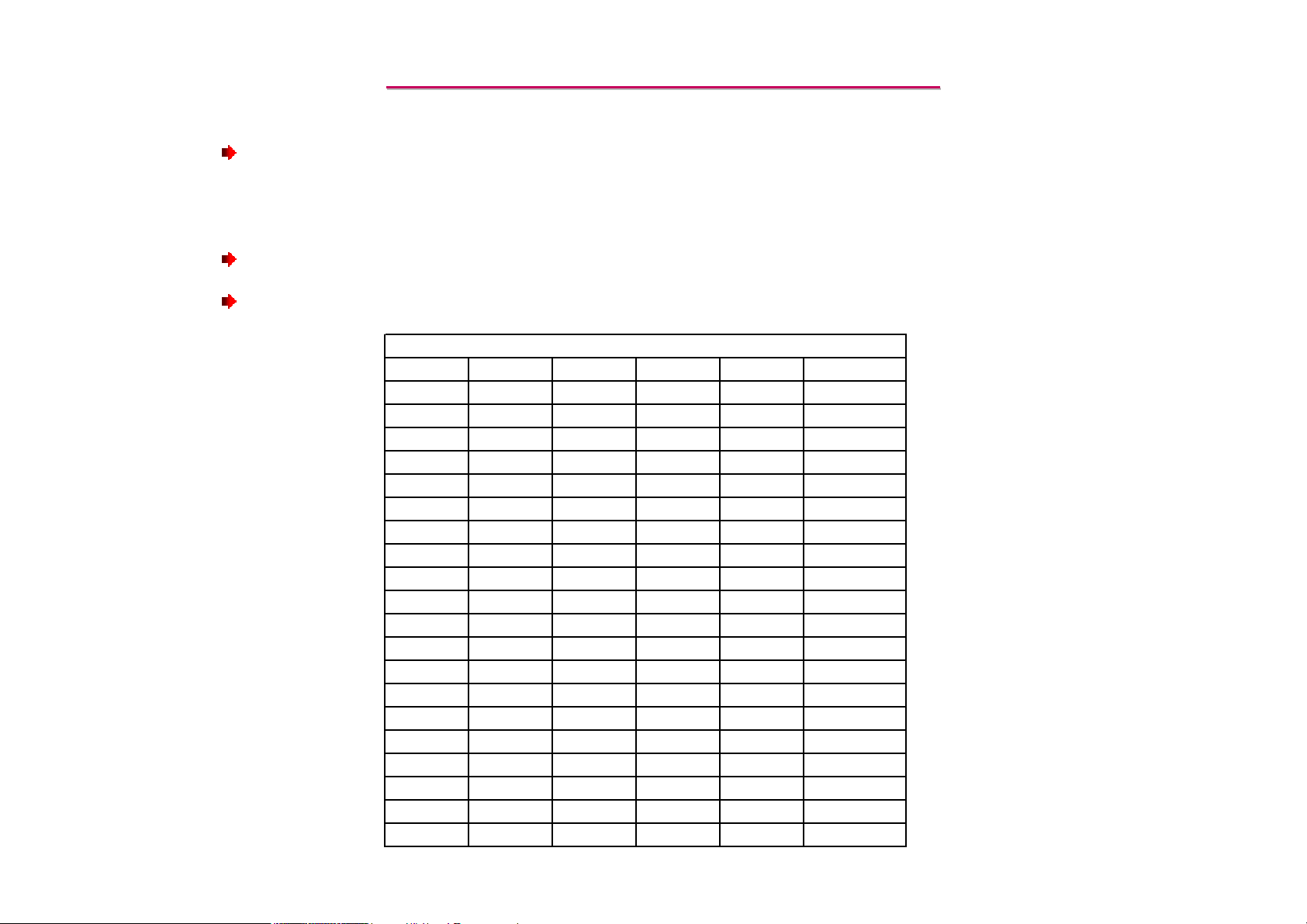
Available at 2 GHz, 2.20 GHz, 2.26 GHz,2.40 GHz, and 2.53 GHz
Binary compatible with applications running on previous members of the Intel microprocessor line
Intel® Net Burst™ micro-architecture
System bus frequency at 400 MHz and 533 MHz
Rapid Execution Engine: Arithmetic Logic Units (ALUs) run at twice the processor core frequency
Hyper Pipelined Technology
Advance Dynamic Execution
----Very deep out-of-order execution
----Enhanced branch prediction
Level 1 Execution Trace Cache stores 12K micro-ops and removes decoder latency from main execution loops
8 KB Level 1 data cache
512 KB Advanced Transfer Cache (on- die, full speed Level 2 (L2) cache) with 8-way associativity and Error
Correcting Code (ECC)
144 Streaming SIMD Extensions 2 (SSE2) instructions
Enhanced floating point and multimedia unit for enhanced video, audio, encryption, and 3D performance
8
LCD PC E--
f
LCD PC E
8188 MAINTENANCE
8188 MAINTENANCE
Power Management capabilities
----System Management mode
----Multiple low-power states
Optimized for 32-bit applications running on advanced 32-bit operating systems
8-way cache associativity provides improved cache hit rate on load/store operations.
Proc es s o r Pins
VI D4 VI D3 VI D2 VI D1 VI D0 Vc c _ M A X
11111VRM output of
111101.100
111011.125
111001.150
110111.175
110101.200
110011.225
110001.250
101111.275
101101.300
101011.325
101001.350
100111.375
100101.400
100011.425
100001.450
011111.475
011101.500
011011.525
011001.550
Table 1.Voltage identification Definition for Desktop Northwood
9

LCD PC E--
LCD PC E
8188 MAINTENANCE
8188 MAINTENANCE
1.2.2 CPU – Intel Celeron Processor In Micro-PGA 478 Package
The Intel® Celeron® processor in the 478-pin package utilizes Flip-Chip Pin Grid Array (FC-PGA2) package
technology, and plugs into a 478-pin surface mount, Zero Insertion Force (ZIF) socket, referred to as the mPGA478B
socket. The Celeron processor in the 478-pin package maintains the tradition of compatibility with IA-32 software.
The Celeron processor in the 478-pin package is designed for uni-processor based Value PC desktop systems.
Features of processor include hyper pipelined technology, a 400 MHz system bus, and an execution trace cache. The
400 MHz system bus is a quad-pumped bus that is clocked with a 100 MHz system clock, making 3.2 GB/sec data
transfer rates possible. The execution trace cache is a first level cache that stores approximately 12k decoded microoperations, which removes the decoder from the main execution path. Additional features include advanced dynamic
execution, advanced transfer cache, enhanced floating point and multi-media unit, and Streaming SIMD Extensions 2
(SSE2). The advanced dynamic execution improves speculative execution and branch prediction internal to the
processor. The advanced transfer cache is a 128 KB, on-die level 2 (L2) cache. The floating point and multimedia
units have 128 bit wide registers with a separate register for data movement. Finally, SSE2 support includes
instructions for double-precision floating point, SIMD integer, and memory management. Power management
capabilities such as AutoHALT, Stop-Grant, Sleep, and Deep Sleep have also been retained. The Celeron processor
in the 478-pin package 400 MHz system bus utilizes a split-transaction, deferred reply protocol. This system bus is
not compatible with the P6 processor family bus. The 400 MHz system bus uses Source-Synchronous Transfer (SST)
of address and data to improve throughput by transferring data four times per bus clock (4X data transfer rate, as in
AGP 4X). Along with the 4X data bus, the address bus can deliver addresses two times per bus clock, and is referred
to as a “double-clocked” or 2X address bus. Working together, the 4X data bus and 2X address bus provide a data bus
bandwidth of up to 3.2 GB/second. Intel will be enabling support components for the Celeron processor in the 478pin package including a heatsink, heat sink retention mechanism, and socket. Manufacturability is a high priority;
hence mechanical assembly can be completed from the top of the motherboard and should not require any special
tooling. The processor system bus uses a variant of GTL+ signaling technology called Assisted Gunning Transceiver
Logic (AGTL+) signalling technology.
10

LCD PC E--
LCD PC E
8188 MAINTENANCE
8188 MAINTENANCE
1.2.2.1 Intel Celeron–Processor Microarchitecture Summary
The following features summarize the Intel Celeron Processor Microarchitecture:
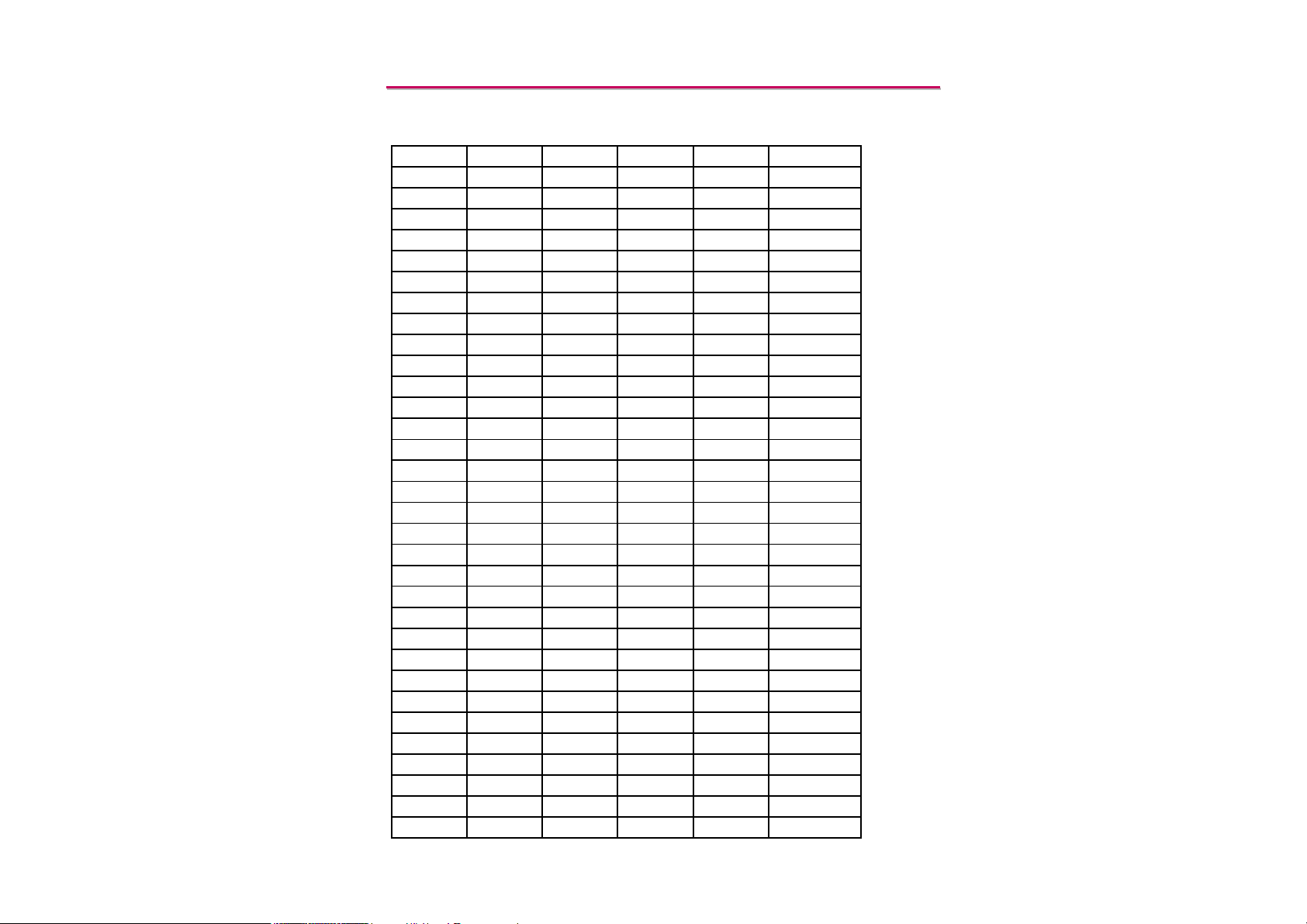
Available at 1.70,1.8G and 1.90 GHz
Binary compatible with applications running on previous members of the Intel microprocessor line
System bus frequency at 400 MHz.
Rapid Execution Engine: Arithmetic Logic Units (ALUs) run at twice the processor core frequency.
Hyper Pipelined Technology.
Advanced Dynamic Execution
----Very deep out-of-order execution
----Enhanced branch prediction
8 KB Level 1 data cache
Level 1 Execution Trace Cache stores 12K micro-ops and removes decoder latency from main execution loops
128 KB Advanced Transfer Cache (on-die,full speed Level 2 (L2) cache) with Error Correction Code (ECC)
144 Streaming SIMD Extensions 2 (SSE2) Instructions
Power Management capabilities
----System Management mode
----Multiple low-power states
Optimized for 32-bit applications running on advanced 32-bit operating systems
11
LCD PC E--
f
LCD PC E
VI D4 VID 3 VID 2 VID 1 VID 0 Vc c _ M A X
11111VRM output of
111101.100
111011.125
111001.150
110111.175
110101.200
110011.225
110001.250
101111.275
101101.300
101011.325
101001.350
100111.375
100101.400
100011.425
100001.450
011111.475
011101.500
011011.525
011001.550
010111.575
010101.600
010011.625
010001.650
001111.675
001101.700
001011.725
001001.750
000111.775
000101.800
000011.825
000001.850
8188 MAINTENANCE
8188 MAINTENANCE
Table 2. Voltage identification Definition for Mobile Northwood
12

LCD PC E--
LCD PC E
8188 MAINTENANCE
8188 MAINTENANCE
1.2.3 Intel 845GE/PE GMCH
1.2.3.1 System Overview:
The 845GE/PE chipsets are a Graphics Memory Controller Hub (GMCH) designed for use with a mPGA478
processor. The GMCH component provides the CPU interface, DDR-SDRAM interface, AGP interface, Hub Interface,
and integrated graphics with several display interfaces (845GE only). The CPU interface supports the Pentium 4
processor subset of the Extended Mode of the Scalable Bus Protocol. The GMCH supports a single channel of DDR
SDRAM. It also supports 1x/2x/4x AGP data transfers and 2x/4x AGP Fast Writes, as defined in the Accelerated
Graphics Port Interface Specification, Revision 2.0 for 1.5V signaling. The integrated graphics controller uses a
portion of system memory for graphics memory (UMA); it does not support Local Memory. The 845GE/PE chipset
platform supports the fourth-generation I/O Controller Hub (ICH4).
1.2.3.2 845GE/PE GMCH Feature List:
Host Interface
--- Supports one physical CPU in a mPGA478 package
--- Supports VTT range from 1.15-1.75 V. The Vtt range is 1.29V – 1.525V for Intel ® Pentium® 4 processor
with 512-KB L2 cache on 0.13 micron process. Supports VTT range from 1.535V – 1.75V for the Pentiun 4
processor with 256-KB L2 cache
--- Supports FSB frequency of 400MHz (100MHz bus clock) and 533MHz (133MHz bus clock)
--- Supports FSB Dynamic Bus Inversion on the data bus
13

LCD PC E--
LCD PC E
--- Supports 32-bit addressing for access to 4 GB of Memory Space
--- Supports 8 deep In Order Queue
--- Supports AGTL+ On-die Termination
System Memory Controller (DDR only)
--- Supports one 64-bit wide DDR SDRAM data channel
--- Available bandwidth up to 2.7GB/s (DDR333)
--- Supports DDR memory only
--- Supports 64-MB, 128-MB, 256-MB, 512-MB SDRAM technologies
--- Supports only x8 and x16 SDRAM devices with four banks
8188 MAINTENANCE
8188 MAINTENANCE
--- Does not support ECC function
--- Registered DIMMs not support
--- Supports unberffered non-ECC DIMMs only
--- Support opportunistic refresh
--- Up to 16, simultaneously open pages (fore per row, four rows maximum)
--- SPD (Serial Presence Detect) scheme for DIMM detection
--- Suspend-to-RAM support using CKE
--- Double Data Rate (DDR) SDRAM configuration
14

LCD PC E--
LCD PC E
Hub Interface
--- Supports Hub Interface 1.5
--- 266MB/s point-to-point Hub Interface to the ICH4
--- 66MHz base clock
--- 1.5V operation
AGP Interface
--- Supports a single 1.5V Accelerated Graphics Port Interface, Specification 2.0-compliant device
--- Support 1x/2x/4x data transfers and 2x/4x Fast Writes
--- 32-deep AGP request queue
--- AGP signals multiplexed with two Intel® DVO port (Intel® 845GE only)
8188 MAINTENANCE
8188 MAINTENANCE
Graphics Features (Intel ® 845GE only)
--- Core Frequency of 266MHz
--- Setup and Render Engine
--- Zone Rendering Support
--- Quality Texture Engine
--- 3D Graphics Rasterization Enhancements
--- 2D Graphics
--- Video DVD/PC-VCR
15

LCD PC E--
LCD PC E
--- Video Overlay
Display (Intel ® 845GE only)
--- Analog Display Support
--- Multiplexed Digital Display Channels
GMCH Package
--- 37.5mm x 37.5mm FC-BGA package with 1 mm ball pitch
--- 1.5V core voltage
Supported FSB/Memory Configurations
8188 MAINTENANCE
8188 MAINTENANCE
--- FSB 400MHz and DDR 200 supported
--- FSB 400/533MHz and DDR 266 supported
--- FSB 533MHz and DDR 333 supported
16

LCD PC E--
LCD PC E
8188 MAINTENANCE
8188 MAINTENANCE
1.2.4 Intel ® 82801DB I/O Controller Hub 4 (ICH4)
1.2.4.1 System Overview:
The ICH4 provides extensive I/O support. Functions and capabilities include:
PCI Local Bus Specification, Revision 2.2-compliant with support for 33 MHz PCI operations.
PCI slots (supports up to 6 Req/Gnt pairs)
ACPI Power Management Logic Support
Enhanced DMA controller, Interrupt controller, and timer functions
Integrated IDE controller supports Ultra ATA100/66/33
USB host interface with support for 6 USB ports; 3 UHCI host controllers; 1 EHCI high-speed
USB 2.0 Host controller
Integrated LAN controller
System Management Bus (SMBus) Specification, Version 2.0 with additional support for I2C devices
Supports Audio Codec ’97, Revision 2.3 specification (a.k.a., AC ’97 Component Specification,
Revision 2.3) Link for Audio and Telephony codecs (up to seven channels)
Low Pin Count (LPC) interface
Firmware Hub (FWH) interface support
Alert On LAN* (AOL) and Alert On LAN 2* (AOL2)
17

LCD PC E--
LCD PC E
8188 MAINTENANCE
8188 MAINTENANCE
1.2.4.2 An overview of the ICH4 capabilities.
Hub Architecture
As I/O speeds increase, the demand placed on the PCI bus by the I/O bridge has become significant. With AC ’97,
USB 2.0, and Ultra ATA/100, coupled with the existing USB, I/O requirements could impact PCI bus performance.
The chipset’s hub interface architecture ensures that the I/O subsystem; both PCI and the integrated I/O features
(IDE, AC ‘97, USB, etc.), receive adequate bandwidth. By placing the I/O bridge on the hub interface (instead of
PCI), the hub architecture ensures that both the I/O functions integrated into the ICH4 and the PCI peripherals
obtain the bandwidth necessary for peak performance.
PCI Interface
The ICH4 PCI interface provides a 33 MHz, Rev. 2.2 compliant implementation. All PCI signals are 5 V tolerant,
except PME#. The ICH4 integrates a PCI arbiter that supports up to six external PCI bus masters in addition to the
internal ICH4 requests.
IDE Interface (Bus Master Capability and Synchronous DMA Mode)
The fast IDE interface supports up to four IDE devices providing an interface for IDE hard disks and ATAPI
devices. Each IDE device can have independent timings. The IDE interface supports PIO IDE transfers up to 16
Mbytes/sec and Ultra ATA transfers up 100 Mbytes/sec. It does not consume any ISA DMA resources. The IDE
interface integrates 16x32-bit buffers for optimal transfers.
The ICH4’s IDE system contains two independent IDE signal channels. They can be electrically isolated
independently. They can be configured to the standard primary and secondary channels (four devices). There are
integrated series resistors on the data and control lines (see Section 5.15 for details).
18

LCD PC E--
LCD PC E
Low Pin Count (LPC) Interface
The ICH4 implements an LPC Interface as described in the LPC 1.0 specification. The Low Pin Count (LPC)
Bridge function of the ICH4 resides in PCI Device 31:Function 0. In addition to the LPC bridge interface function,
D31:F0 contains other functional units including DMA, Interrupt controllers, Timers, Power Management, System
Management, GPIO, and RTC.
Note that in the current chipset platform, the Super I/O (SIO) component has migrated to the Low Pin Count (LPC)
interface. Migration to the LPC interface allows for lower cost Super I/O designs.
Compatibility Modules (DMA Controller, Timer/Counters, Interrupt Controller)
The DMA controller incorporates the logic of two 82C37 DMA controllers, with seven independently
programmable channels. Channels 0–3 are hardwired to 8-bit, count-by-byte transfers, and channels 5–7 are
hardwired to 16-bit, count-by-word transfers. Any two of the seven DMA channels can be programmed to support
8188 MAINTENANCE
8188 MAINTENANCE
fast Type-F transfers.
The ICH4 supports two types of DMA (LPC and PC/PCI). DMA via LPC is similar to ISA DMA. LPC DMA and
PC/PCI DMA use the ICH4’s DMA controller. The PC/PCI protocol allows PCI-based peripherals to initiate DMA
cycles by encoding requests and grants via two PC/PCI REQ#/GNT# pairs.
LPC DMA is handled through the use of the LDRQ# lines from peripherals and special encodings on LAD[3:0]
from the host. Single, Demand, Verify, and Increment modes are supported on the LPC interface. Channels 0–3 are
8-bit channels. Channels 5–7 are 16-bit channels. Channel 4 is reserved as a generic bus master request.
The timer/counter block contains three counters that are equivalent in function to those found in one 82C54
programmable interval timer. These three counters are combined to provide the system timer function, and speaker
tone. The 14.31818 MHz oscillator input provides the clock source for these three counters.
19

LCD PC E--
LCD PC E
The ICH4 provides an ISA-Compatible Programmable Interrupt Controller (PIC) that incorporates the functionality
of two 82C59 interrupt controllers. The two interrupt controllers are cascaded so that 14 external and two internal
interrupts are possible. In addition, the ICH4 supports a serial interrupt scheme.
All of the registers in these modules can be read and restored. This is required to save and restore system state after
power has been removed and restored to the platform.
Advanced Programmable Interrupt Controller (APIC)
In addition to the standard ISA compatible Programmable Interrupt Controller (PIC) described in the previous
section, the ICH4 incorporates the Advanced Programmable Interrupt Controller (APIC).
Universal Serial Bus (USB) Controller
The ICH4 contains an Enhanced Host Controller Interface (EHCI) compliant host controller that supports USB
high-speed signaling. High-speed USB 2.0 allows data transfers up to 480 Mb/s which is 40 times faster than full-
8188 MAINTENANCE
8188 MAINTENANCE
speed USB. The ICH4 also contains three Universal Host Controller Interface (UHCI) controllers that support USB
full-speed and low-speed signaling.
The ICH4 supports 6 USB 2.0 ports. All six ports are high-speed, full-speed, and low-speed capable. ICH4’s portrouting logic determines whether a USB port is controlled by one of the UHCI controllers or by the EHCI controller.
LAN Controller
The ICH4’s integrated LAN controller includes a 32-bit PCI controller that provides enhanced scatter-gather bus
mastering capabilities and enables the LAN controller to perform high-speed data transfers over the PCI bus. Its bus
master capabilities enable the component to process highlevel commands and perform multiple operations; thisoffloading communication tasks from the processor. Two large transmit and receive FIFOs of 3 KB each help prevent
20

LCD PC E--
LCD PC E
data underruns and overruns while waiting for bus accesses. This enables the integrated.
LAN controller to transmit data with minimum interframe spacing (IFS). The LAN controller can operate in either
full duplex or half duplex mode. In full duplex mode the LAN controller adheres with the IEEE 802.3x Flow Control
specification. Half duplex performance is enhanced by a proprietary collision reduction mechanism.
RTC
The ICH4 contains a Motorola MC146818A-compatible real-time clock with 256 bytes of batterybacked RAM.
The real-time clock performs two key functions: keeping track of the time of day and storing system data, even
when the system is powered down. The RTC operates on a 32.768 KHz crystal and a separate 3 V lithium battery
that provides up to seven years of protection.
The RTC also supports two lockable memory ranges. By setting bits in the configuration space, two 8-byte
ranges can be locked to read and write accesses. This prevents unauthorized reading of passwords or other system
security information.
8188 MAINTENANCE
8188 MAINTENANCE
The RTC also supports a date alarm that allows for scheduling a wake up event up to 30 days in advance, rather
than just 24 hours in advance.
GPIO
Various general purpose inputs and outputs are provided for custom system design. The number of inputs and
outputs varies depending on ICH4 configuration.
Enhanced Power Management
The ICH4’s power management functions include enhanced clock control, local and global monitoring support
for 14 individual devices, and various low-power (suspend) states (e.g., Suspend-to-DRAM and Suspend-to-Disk).
21

LCD PC E--
LCD PC E
A hardware-based thermal management circuit permits software-independent entrance to low-power states. The
ICH4 contains full support for the Advanced Configuration and Power Interface (ACPI) Specification, Revision 2.0.
System Management Bus (SMBus 2.0)
The ICH4 contains an SMBus Host interface that allows the processor to communicate with SMBus slaves. This
interface is compatible with most I2C devices. Special I2C commands are implemented.
The ICH4’s SMBus host controller provides a mechanism for the processor to initiate communications with
SMBus peripherals (slaves). Also, the ICH4 supports slave functionality, including the Host Notify protocol. Hence,
the host controller supports 8 command protocols of the SMBus interface (see System Management Bus (SMBus)
Specification, Version 2.0): Quick Command, Send Byte, Receive Byte, Write Byte/Word, Read Byte/Word,
Process Call, Block Read/Write, and Host Notify.
8188 MAINTENANCE
8188 MAINTENANCE
Manageability
The ICH4 integrates several functions designed to manage the system and lower the total cost of ownership (TC0) of
the system. These system management functions are designed to report errors, diagnose the system, and recover from
system lockups without the aid of an external microcontroller.
1.TCO Timer. The ICH4’s integrated programmable TCO Timer is used to detect system locks. The first expiration
of the timer generates an SMI# that the system can use to recover from a software lock.. The second expiration of
the timer causes a system reset to recover from a hardware lock.
2. Processor Present Indicator. The ICH4 looks for the processor to fetch the first instruction after reset. If the
processor does not fetch the first instruction, the ICH4 will reboot the system.
22

LCD PC E--
LCD PC E
3. ECC Error Reporting. When detecting an ECC error, the host controller has the ability to send one of several
messages to the ICH4. The host controller can instruct the ICH4 to generate either an SMI#, NMI, SERR#, or
TCO interrupt.
4. Function Disable. The ICH4 provides the ability to disable the following functions: AC ’97 Modem, AC ’97
Audio, IDE, LAN, USB, or SMBus. Once disabled, these functions no longer decode I/O, memory, or PCI
configuration space. Also, no interrupts or power management events are generated from the disable functions.
5. Intruder Detect. The ICH4 provides an input signal (INTRUDER#) that can be attached to a switch that is
activated by the system case being opened. The ICH4 can be programmed to generate an SMI# or TCO interrupt
due to an active INTRUDER# signal.
6. SMBus 2.0. The ICH4 integrates an SMBus controller that provides an interface to manage peripherals (e.g.,
serial presence detection (SPD) and thermal sensors) with host notify capabilities.
7. Alert On LAN*. The ICH4 supports Alert On LAN and Alert On LAN 2. In response to a TCO event (intruder
8188 MAINTENANCE
8188 MAINTENANCE
detect, thermal event, processor not booting) the ICH4 sends a message over the SMBus. A LAN controller can
decode this SMBus message and send a message over the network to alert the network manager.
AC ’97 2.3 Controller
The Audio Codec ’97, Revision 2.3 specification defines a digital interface that can be used to attach an audio
codec (AC), a modem codec (MC), an audio/modem codec (AMC) or a combination of ACs and MC. The AC ’97
specification defines the interface between the system logic and the audio or modem codec, known as the AC-link.
By using an audio codec, the AC-link allows for cost-effective, high-quality, integrated audio on Intel’s chipsetbased platform. In addition, an AC ’97 soft modem can be implemented with the use of a modem codec. Several
system options exist when implementing AC ’97. The ICH4-integrated digital link allows several external
23

LCD PC E--
LCD PC E
codecs to be connected to the ICH4. The system designer can provide audio with an audio codec, a modem with a
modem codec, or an integrated audio/modem codec. The digital link is expanded to support three audio codecs or
two audio codecs and one modem codec.
The modem implementations for different countries must be taken into consideration, because telephone systems
may vary. By using a split design, the audio codecs can be on-board and the modem codec can be placed on a riser.
The digital link in the ICH4 supports the Audio Codec ’97, Revision 2.3 specification, so it supports three codecs
with independent PCI functions for audio and modem. Microphone input and left and right audio channels are
supported for a high quality, two-speaker audio solution. Wake on Ring from Suspend also is supported with the
appropriate modem codec.
The ICH4 expands the audio capability with support for up to six channels of PCM audio output (full AC3
decode). Six-channel audio consists of Front Left, Front Right, Back Left, Back Right, Center, and Subwoofer, for
a complete surround-sound effect. ICH4 has expanded support for three audio codecs on the AC-link.
8188 MAINTENANCE
8188 MAINTENANCE
24
LCD PC E--
LCD PC E
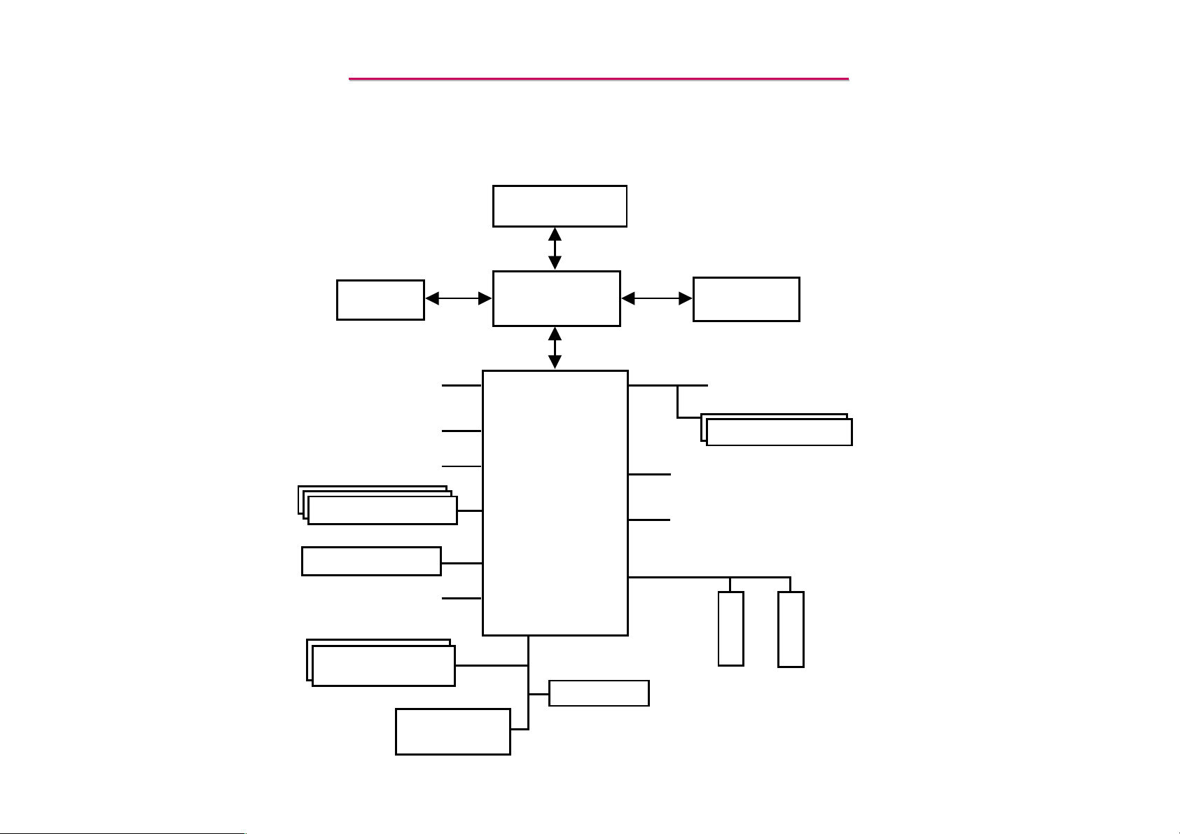
1.2.4.3 System configuration:
8188 MAINTENANCE
8188 MAINTENANCE
Processor
AGP
USB
(Supports 6
USB 2.0 ports)
IDE-Primary
IDE-Secondary
AC’97 Codec(s)
LAN Connect
GPIO
Firmware Hub(s)
(1-8)
Host Controller
Intel
82801 DB ICH4
LPC Interface
Super I/O
Memory
Power Management
Clock Generators
System Management (TCO)
SMBus/I2C
PCI Bus
Slot
Slot
Other ASICs
(Optional)
25

LCD PC E--
LCD PC E
8188 MAINTENANCE
8188 MAINTENANCE
1.2.5 Video Controller
1.2.5.1 ATI M9-CPS64 (RADEON Mobility 9000)
M9-CSP64 (RADEON MOBILITY 9000) has 64MB of integrated DDR memory (128-bit, 2 channels), with no
memory expansion capability. It support DirectX8.1 and AGP4X
Introduction
The RADEON MOBILITY 9000 provides the fastest and most advanced 2D, 3D, and multimedia graphics
performance for the latest applications in full 32-bit color. Its architecture introduces the latest achievements in the
graphics industry, which enable the use of the progressive new features in upcoming applications, but without
compromising performance. ATI’s exclusive support of DirectX® 8.1 features, highly optimized OpenGL®
support, and flexible memory configurations allow implementations targeted at both gaming enthusiast and
workstation platforms.
SMARTSHADER™ — Advanced Shader Technology
1. Provides complete hardware-accelerated support for the new DirectX® 8.1 programmable shader
model, enabling more complex and realistic texture and lighting effects than ever before.
2. Significant improvement over first-generation shaders introduced in DirectX® 8.1, with a much more
powerful and intuitive instruction set.
3. Offers full support for this feature in OpenGL® 1.3 applications.
26

LCD PC E--
LCD PC E
SMOOTHVISION™ — Flexible Anti-Aliasing
1. The most flexible and efficient anti-aliasing implementation available to date.
2. Eliminates “jaggies” on the edges of objects, shimmering pixels on distant surfaces, and other visual
artifacts for smoother-looking images.
3. Unique adaptive process can independently select the anti-aliasing pattern for each pixel within a 4x4 region,
rather than relying on a fixed pattern for the whole image.
4. Better visual quality with minimal performance degradation.
5. Supports DirectX® 8.1 multisampling and related effects, including motion blur and depth-of-field.
High Performance Memory Support
1. Incorporates support for DDR SDRAM/SGRAM at up to 220 MHz.
8188 MAINTENANCE
8188 MAINTENANCE
2. Features ATI’s second generation HYPER Z™ II technology that conserves memory bandwidth for improved
performance in demanding applications.
3. Boosts effective memory bandwidth by over 20%.
Dual Display Support
1. Leading-edge technology, fully optimized with HYDRA VISION™, flexibly supports multiple
combinations of traditional CRT monitors, flat panel displays and TV.
2. Features Dual Channel DVI support.
3. Integrated TMDS transmitter supports panels up to UXGA (1600x1200) resolution.
4. Improved RAMDAC speed of 400MHz.
27

LCD PC E--
LCD PC E
CHARISMA ENGINE™ II
CHARISMA ENGINE™ II, the RADEON MOBILITY 9000 geometry engine, delivers up to 50 milliontrans
formed, clipped, and lit triangles /second peak processing capability. Additionally, the engine implements a fully
compliant DirectX® 8.1 Programmable Vertex Shader.
PIXEL TAPESTRY™ II
PIXEL TAPESTRY™ II, the RADEON MOBILITY 9000 3D rendering engine, utilizes 4 parallel pipelines
each capable of handling up to 6 textures in a single pass, delivering an incredible 1.2 gigatexels per second fill
rate for maximum 32 bit color performance at the highest resolutions.
VIDEO IMMERSION™ II
VIDEO IMMERSION™ II technology allows integration of industry leading digital video features, including
8188 MAINTENANCE
8188 MAINTENANCE
advanced de-interlacing and frame rate conversion algorithms for unprecedented video quality and integrated digital
TV decode capability. Includes programmable, independent gamma control for the video overlay.
Combined with a tuner and demodulator, RADEON MOBILITY 9000 provides an all-format DTV/HDTV
solution, even including the 1920 pixel wide 1080i format. Coupled with the RAGE THEATER analog
encoder/decoder chip, RADEON MOBILITY 9000 provides a complete convergence solution.
Ideal for Windows 2000 and Windows XP
RADEON MOBILITY 9000 provides comprehensive support for all new Windows 2000 and Windows XP
display-oriented features, including acceleration of new GDI extensions like Alpha BLTs, Transparent BLTs, and
Gradient Fills, as well as exclusive, patent-pending hardware alpha cursor support.
28

LCD PC E--
LCD PC E
General and Interfacing Features
1. 32-bit PCI bus (Rev 2.2), 3.3 V with bus mastering support.
2. Comprehensive AGP support including 3.3 Volt (AGP 2X) and 1.5 Volt (AGP 4X) mode operation, sideband
addressing, AGP texturing (direct memory execution), and support for AGP reads and writes, including fast
write capability.
3. Single channel 128/64-bit memory interface using SGRAM or SDRAM to build 8/16/32/64 MB configurations.
Operating frequency is 67MHz minimum to 220MHz maximum, SDR or DDR.
4. 16-bit Zoom Video port.
5. Support for ROM or Flash RAM parallel or serial video BIOS.
6. Two independent CRT controllers to support two asynchronous simultaneous display paths.
7. Integrated DAC for CRT with stereoscopic display support.
8188 MAINTENANCE
8188 MAINTENANCE
8. Integrated second DAC for the second CRT (TV) support.
9. Integrated LVDS interface: single and dual pixel per clock, up to 85MHz per channel.
10. LCD panel detection.
11. Integrated TMDS transmitter running up to 165MHz (when matched with coherently clocked receiver;
otherwise, 135MHz) for support up to 1600x1200 at 60Hz. Fully compliant with DVI and DFP connection
standards. Ratiometric expansion.
12. Support for external TMDS transmitter via 24-bit digital output to drive most popular TMDS transmitters up to
165MHz frequency.
13. Internal and external Spread Spectrum support.
29
 Loading...