

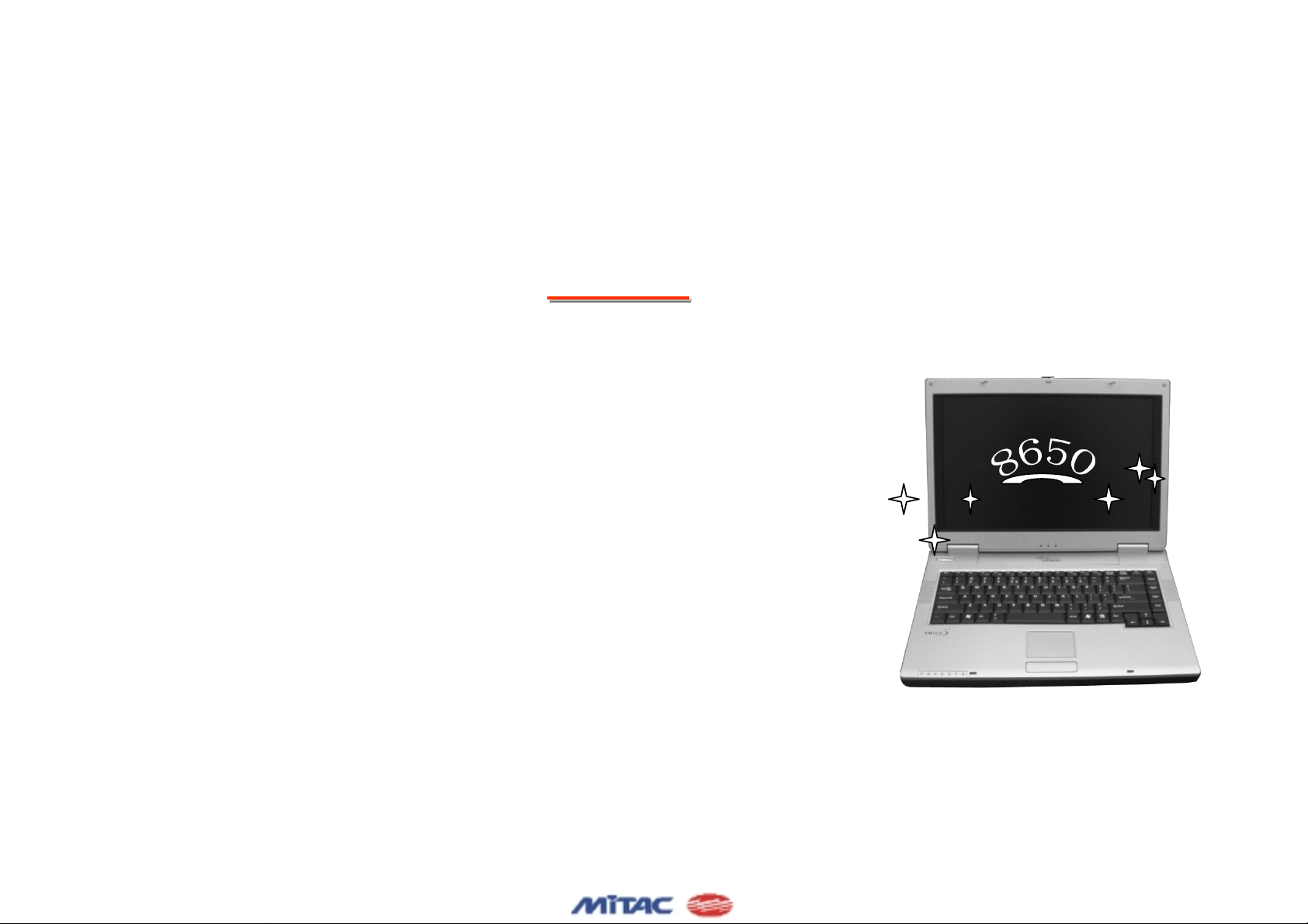
MiTAC 8650 Service Manual
SERVICE MANUAL FOR
SERVICE MANUAL FOR
SERVICE MANUAL FOR
8650
8650
86508650
8650
8650
86508650
8650
8650
86508650
BY: Sanny.Gao
Repair Technology Research Department /EDVD
Repair Technology Research Department /EDVD
November. 2005/R01
Contents
8650 N/B Maintenance
8650 N/B Maintenance
1. Hardware Engineering Specification …………………………………………………………………..
1.1 Introduction ……………………………………………………………………………………………………………
1.2 System Hardware Parts ………………………………………………………………………………………………
1.3 Other Functions ……………………………………………………………………………………………………….
1.4 Power Management …………………………………………………………………………………………………..
1.5 Appendix 1: VIA VT8235CE GPIO Definitions ……………………………………………………………………
1.6 Appendix 2: W83L950D KBC Pins Definitions …………………………………………………………………….
1.7 Appendix 3: 8650 External Specification ……………………………………………………………………………
2. System View and Disassembly ………………………………………………………………………….
2.1 System View ……………………………………………………………………………………………………………
2.2 Tools Introduction …………………………………………………………………………………………………….
2.3 System Disassembly …………………………………………………………………………………………………..
MiTac Secret
3. Definition & Location of Connectors/Switches ………………………………………………………
4
4
6
33
39
43
45
48
51
51
54
55
75
3.1 Mother Board (side A) ………………………………………………………………………………………………..
3.2 Mother Board (side B) ………………………………………………………………………………………………..
Confidential Document
4. Definition & Location of Major Components …………………………………………………………
4.1 Mother Board (side A) ………………………………………………………………………………………………..
4.2 Mother Board (side B) ………………………………………………………………………………………………..
75
77
78
78
79
1
Contents
8650 N/B Maintenance
8650 N/B Maintenance
5. Pin Description of Major Components ….……………………………………………………………..
5.1 Intel Pentium M Processor CPU ……………………………………………………………………………………..
5.2 PN800 North Bridge …………………………………………………………………………………………………..
5.3 VT8235CE South Bridge ….………………………………………………………………………………………….
6. System Block Diagram ………………………………………………………………………………….
7. Maintenance Diagnostics ………………………………………………………………………………..
7.1 Introduction ……………………………………………………………………………………………………………
7.2 Error Codes ……………………………………………………………………………………………………………
7.3 Debug Tool …………………………………………………………………………………………………………….
MiTac Secret
8. Trouble Shooting ………………………………………………………………………………………..
8.1 No Power ………………………………………………………………………………………………………………
8.2 No Display ……………………………………………………………………………………………………………..
8.3 LCD No Display or Picture Abnormal ………………………………………………………………………………
8.4 External Monitor No Display or Color Abnormal ………………………………………………………………….
8.5 Memory Test Error …………………………………………………………………………………………………..
8.6 Keyboard (K/B) Touch-Pad (T/P) Test Error ………………………………………………………………………
8.7 Hard Disk Drive Test Error ………………………………………………………………………………………….
8.8 CD-ROM Drive Test Error …………………………………………………………………………………………..
8.9 USB Port Test Error ………………………………………………………………………………………………….
Confidential Document
80
80
84
95
105
106
106
107
109
110
112
118
121
124
126
128
130
132
134
2
Contents
8650 N/B Maintenance
8650 N/B Maintenance
8.10 PC Card Socket Test Error …………………………………………………………………………………………
8.11 Mini-PCI Socket Test Error ……………………………………………………………………………………….
8.12 Audio Test Error …………………………………………………………………………………………………….
8.13 LAN Test Error ………….…………………………………………………………………………………………..
9. Spare Parts List ……………………………………………………………………………… ………….
10. System Exploded Views ………………………………………………………………………………..
11. Reference Material …………………………………………………………………………………….
MiTac Secret
137
139
141
144
146
157
161
Confidential Document
3
8650 N/B Maintenance
8650 N/B Maintenance
1. Hardware Engineering Specification
1.1 Introduction
1.1.1 General Description
This document describes the brief introduction for MITAC 8650 portable notebook computer system.
1.1.2 System Overview
MiTac Secret
The MITAC 8650 model is designed for Intel Banias processor with 400 MHz FSB with Micro-FCPGA package.
It can support Banias 1.5 G~1.9 GHz.
This system is based on PCI architecture and is fully compatible with IBM PC/AT specification, which has standard
hardware peripheral interface. The power management complies with Advanced Configuration and Power Interface
(ACPI) 2.0. It also provides easy configuration through CMOS setup, which is built in system BIOS software and
can be pop-up by pressing F2 key at system start up or warm reset. System also provides icon LEDs to display
system status, such as Wireless LAN indicator, Power indicator, Battery status indicator, ODD, HDD, Num Lock,
Caps Lock, Scroll Lock. It also equipped with LAN, 56 K Fax Modem, 3 USB ports, and audio line out, external
microphone function.
Confidential Document
4
8650 N/B Maintenance
8650 N/B Maintenance
The memory subsystem supports two expansion DDR SDRAM slot with unbuffered PC3200 DDR400 SDRAM.
The VIA PN800 Mobile North Bridge integrates a high performance CPU interface for Intel Pentium 4/Pentium-M
processor, a full featured AGP port controller, Integrated Graphics with 2D/3D/Video Controllers, a advanced
high-performance DDR400 SDRAM controller, and high bandwidth Ultra V-Link host controller connecting with
VIA VT8235CE South Bridge.
The VIA VT8235CE integrates Universal Serial Bus 2.0 Host Controllers Interface (UHCI), the Audio Controller
With AC97 interface, the Ethernet includes a 32-bit PCI controller, the IDE Master/Slave controllers, and Inter-
operable with VIA Host-to-V-Link Host Controller.
The VIA VT6103L is a Fast Ethernet 10/100 1-port PHY/Transceiver with MII interface, and meet all applicable
IEEE 802.3, 10Base-T and 100Base-Tx standards.
The ENE CB1410 CardBus controller functions as a single slot PCI to Cardbus bridge. The CB1410 compliant
with PCI Local Bus Specification Rev2.2, PC99 System Design Guide, and PC Card Standard 8.0.
The W83L950D is a high performance microcontroller on-chip supporting functions optimized for embedded
control. These include ROM, RAM, four types of timers, a serial communication interface, optional I²C bus
interface, host interface, A/D converter, D/A converter, I/O ports, and other functions needed in control system
configurations, so that compact, high performance systems can be implemented easily.
A full set of software drivers and utilities are available to allow advanced operating systems such as Windows ME,
Windows 2000 and Windows XP to take full advantage of the hardware capabilities. Features such as bus
mastering IDE, plug and play, Advanced Power Management (APM) with application restart, software-controlled
power shutdown.
Confidential Document
MiTac Secret
5
8650 N/B Maintenance
8650 N/B Maintenance
Following chapters will have more detail description for each individual sub-systems and functions.
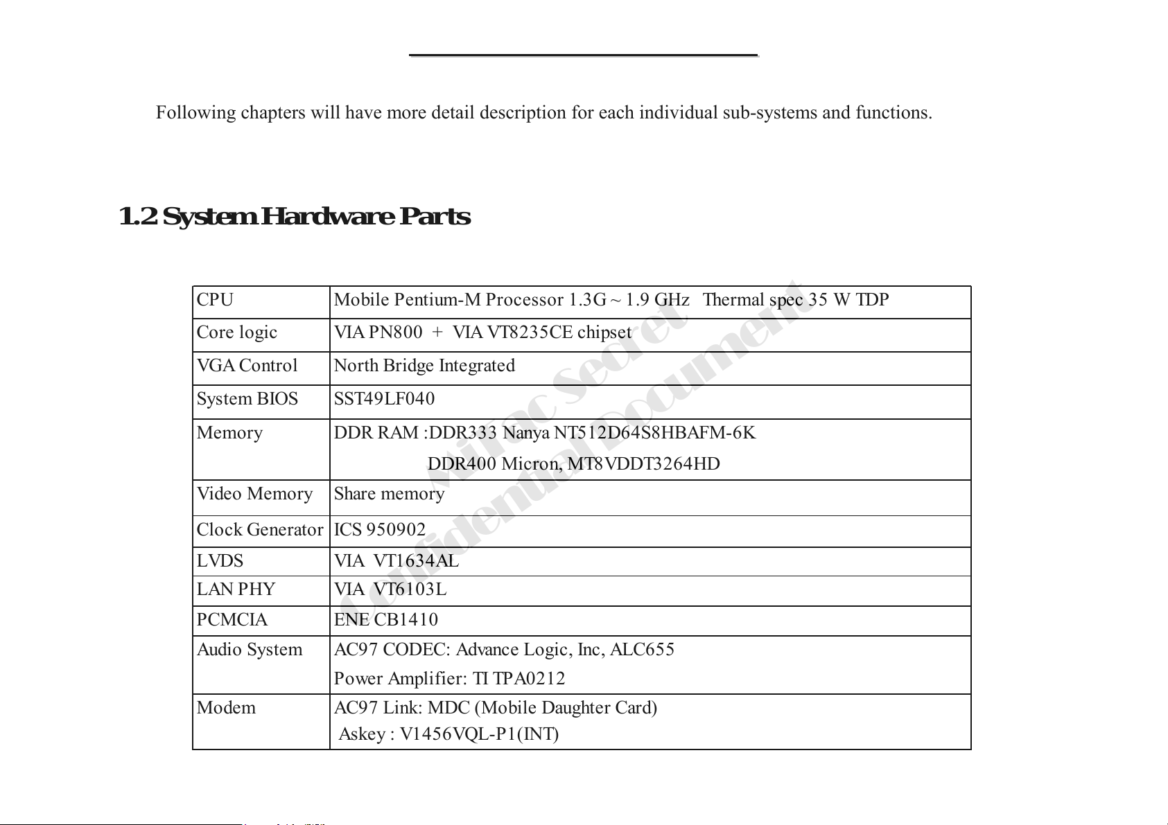
1.2 System Hardware Parts
CPU Mobile Pentium-M Processor 1.3G ~ 1.9 GHz Thermal spec 35 W TDP
Core l ogic VIA P N800 + VIA VT82 35CE chipset
VGA Control North Bridge Integrated
System BIOS SST49LF040
Memory
Video Memory Share memory
Clock Generator ICS 950902
LVDS VIA VT163 4AL
LAN PHY VIA VT6103L
PCMCIA ENE CB1410
Audio System
Modem
DDR RAM :DDR333 Nanya NT512D64S8HBAFM-6K
DDR400 Micron, MT8VDDT3264HD
MiTac Secret
Confidential Document
AC97 CODEC: Advance Logic, Inc, ALC655
Power Amplifier: TI TPA0212
AC97 Link: MDC (Mobile Daughter Card)
Askey : V1456VQL-P1(INT)
6
8650 N/B Maintenance
8650 N/B Maintenance
1.2.1 Intel Banias Processors in Micro-FCPGA Package
Intel Banias Processors with 593 pins Micro-FCBGA package.
It has the Intel NetBurst micro-architecture which features include hyper-pipelined technology, a rapid execution
engine, a 400 MHz system, an execution trace cache, advanced dynamic execution, advanced transfer cache,
enhanced floating point and multi-media unit, and Streaming SIMD Extensions 2 (SSE2).
The Streaming SIMD Extensions 2 (SSE2) enable break-through levels of performance in multimedia applications
including 3-D graphics, video decoding/encoding, and speech recognition.
Use Source-Synchronous Transfer (SST) of address and data to improve performance by transferring data four
times per bus clock.
Support Enhanced Intel SpeedStep technology, which enables real-time dynamic switching of the voltage and
frequency between two performance modes.
MiTac Secret
1.2.2 Clock Generator
Confidential Document
The ICS950902 is a single chip clock solution for desktop designs using the VIA P4X/P4M/KT/KN266/333 style
chipsets with PC133 or DDR memory. The ICS950902 is part of a whole new line of ICS clock generators and
buffers called TCH™ (Timing Control Hub). This part incorporates ICS's newest clock technology which offers
more robust features and functionality. Employing the use of a serially programmable I2C interface, this device can
adjust the output clocks by configuring the frequency setting, the output divider ratios, selecting the ideal spread
7
8650 N/B Maintenance
8650 N/B Maintenance
percentage, the output skew, the output strength, and enabling/disabling each individual output clock. M/N
control can configure output frequency with resolution up to 0.1 MHz increment.
Recommended Application
VIA P4X/P4M/KT/KN266/333 style chipsets
Output Features
• 1- Pair of differential CPU clocks @ 3.3 V (CK408) /1- Pair of differential open drain CPU clocks (K7)
• 1- Pair of differential push pull CPU_CS clocks @ 2.5 V
• 3- AGP @ 3.3 V
• 7- PCI @ 3.3 V (1- Free running)
• 1- 48 MHz @ 3.3 V fixed
MiTac Secret
Confidential Document
• 1- 24_48 MHz @ 3.3 V (Default 48 MHz I2C select only)
• 2- REF @ 3.3 V, 14.318 MHz
• 12- SDRAM (6 pair - DDR) selectable
8

8650 N/B Maintenance
8650 N/B Maintenance
Features/Benefits
• Programmable output frequency
• Programmable output divider ratios
• Programmable output rise/fall time
• Programmable output skew
• Programmable spread percentage for EMI control
• DDR output buffer supports up to 200 MHz
• Watchdog timer technology to reset system if system malfunctions
• Programmable watch dog safe frequency
• Support I2C Index read/write and block read/write operations
• Uses external 14.318 MHz crystal
MiTac Secret
Confidential Document
1.2.3 PN800 Mobile North Bridge
The PN800 is a high performance, cost-effective and energy efficient UMA North Bridge with integrated
UniChrome Pro graphics/video controllers used for the implementation of mobile personal computer systems
9
8650 N/B Maintenance
8650 N/B Maintenance
based on 800/533/400 MHz FSB Intel Pentium 4 and Pentium M super-scalar processors.The complete mobile
chipset consists of the PN800 North Bridge (829 pin HSBGA) and the VT8235-CE V-Link South Bridge (539-pin
BGA). The PN800 integrates VIA’s PT800 system controller with high-performance UniChrome Pro 3D/2D
graphics accelerator plus flat panel, DVI monitor and TV out interfaces. The PN800 provides superior performance
between the CPU,DRAM, V-Link bus and internal AGP 8x graphics controller bus with pipelined, burst, and
concurrent operation. The VT8235-CE is a highly integrated peripheral controller which includes V-Link-to-PCI/
V-Link-to-LPC controllers, Ultra DMA IDE controller,USB2.0 host controller, 10/100 Mb networking MAC,
AC97, and system power management controllers.
Host CPU Interface
The PN800 supports 800/533/400 MHz FSB Intel Pentium 4 and Pentium M super-scalar processors. It implements
a twelve level In-Order-Queue and supports Intel Hyper-Threading Technology to maximize system performance
for multi-threaded software applications. DBI and Pentium M bus protocol, as well as Intel Speed Step Technology,
are supported which effectively reduce overall system power consumption.
AGP Interface
MiTac Secret
Confidential Document
The PN800 AGP controller is AGP 3.0 compliant with up to 2.1 GB/second data transfer rate capability. It
supports asynchronous AGP and CPU interfaces for flexible system configuration. Deep read (1024-byte) and
write (512-byte) FIFOs are integrated for optimal bus utilization and minimum data transfer latency.
10
8650 N/B Maintenance
8650 N/B Maintenance
Memory Controller
The PN800 SDRAM Controller supports two sets of 64-bit memory data, address and control signals to minimize
signal loading and up to 4 double-sided DDR400/333/266 DIMMs for 8 GB maximum physical memory. The
DDR DRAM interface allows zero wait-state data transfer bursting between the DRAM and the memory
controller’s data buffers. The different banks of DRAM can be composed of an arbitrary mixture of
64/128/256/512/1024 Mb DRAMs in x8 and x16 configurations. The DRAM controller can run either
synchronous or pseudo-synchronous with the host CPU bus. The PN800 North Bridge is pin compatible with the
PN880 North Bridge which connects to the memory modules in exactly the same manner while supporting true
128-bit operation (simultaneous memory access on both sets of 64-bit memory data/address/control signals).
Ultra V-Link
The PN800 North Bridge interfaces to the South Bridge through a high speed (up to 1 GB/sec) 8x, 66 MHz
Data Transfer interconnect bus called “Ultra V-Link”. Deep pre-fetch and post-write buffers are included to
allow for concurrent CPU and V-link operation. The combined PN800 North Bridge and VT8235-CE South
Bridge system supports enhanced PCI bus commands such as “Memory-Read-Line”, “Memory-Read-Multiple”
and “Memory-Write-Invalid” commands to minimize snoop overhead.In addition, advanced features are
supported such as CPU write-back forward to PCI master, and CPU write-back merged with PCI post write
buffers to minimize PCI master read latency and DRAM utilization. Delay transaction and read caching
mechanisms are also implemented for further improvement of overall system performance.
Confidential Document
MiTac Secret
11
8650 N/B Maintenance
8650 N/B Maintenance
System Power Management
For sophisticated power management, the PN800 supports dynamic CKE control to minimize DDR SDRAM
power consumption during normal system state (S0). A separate suspend power plane is implemented for the
memory control logic for Suspend-to-DRAM state. Enhanced Intel Speed Step™ Technology enables
minimization of CPU power consumption while sustaining processing power. The PN800 graphics accelerator
implements dynamic clock gating for inactive functions to achieve maximum power savings. The system can also
be switched to standby or suspend states to further reduce power consumption when idle.Automatic panel power
sequencing and VESA DPMS (Display Power Management Signaling) CRT power-down are supported. Coupled
with the VT8235-CE South Bridge chip, a complete power conscious PC main board can be implemented with no
external glue logic.
3D Graphics Engine
MiTac Secret
Featuring an integrated 128-bit 3D graphics engine, the PN800 North Bridge utilizes a highly pipelined
architecture that provides high performance along with superior image quality. Several new features enhance
the 3D architecture, including two pixel rendering pipes, single-pass multitexturing, bump and cubic mapping,
texture compression, edge anti-aliasing, vertex fog and fog table, hardware back-face culling, specular lighting,
anisotropic filtering, and an 8-bit stencil buffer. The chip also offers the industry’s only simultaneous usage of
single-pass multitexturing and single-cycle trilinear filtering – enabling stunning image quality without
performance loss. Image quality is further enhanced with true 32-bit color rendering throughout the 3D pipeline
to produce more vivid and realistic images. The advanced triangle setup engine provides industry leading 3D
performance for a realistic user experience in games and other interactive 3D applications. The 3D engine is
optimized for AGP texturing from system memory.
Confidential Document
12
8650 N/B Maintenance
8650 N/B Maintenance
128-bit 2D Graphics Engine
The PN800 North Bridge's advanced 128-bit 2D graphics engine delivers high-speed 2D acceleration for
productivity applications. The enhanced 2D architecture with direct access frame buffer capability optimizes
UMA performance and provides acceleration of all color depths. The PN800 North Bridge provides the ideal
architecture for high quality MPEG-2 based video applications. For MPEG video playback, the integrated video
engine offloads the CPU by performing planar-to-packed format conversion and motion video compensation
tasks, while its enhanced scaling algorithm delivers incredible full-screen video playback.
Video Capture
The PN800 North Bridge implements an optional Video Capture Port which supports various video capture
standards, including ITU-R BT656, VIP 1.1 and VIP 2.0 and is compliant with the most common video
capture formats: 16/32-bit RGB and YUV422. With the integrated video capture feature, the PN800 can
provide high performance video effects for video capturing and playback.
LCD, DVI Monitor and TV Output Display Support
MiTac Secret
Confidential Document
The PN800 provides three “Digital Video Port” interfaces: FPDP, GDVP1, and DVP0. The Flat Panel Display
Port (FPDP) implements a 24-bit/dual 12-bit interface which is designed to drive a Flat Panel Display via an
external LVDS transmitter chip (such as the VIA VT1631, NSC DS90C387R or Chrontel CH7017). The
PN800 can be connected to the external LVDS transmitter chip in either 24-bit or dual-12-bit modes. A wide
variety of LCD panels are supported including VGA, SVGA, XGA, SXGA+ and up to UXGA-resolution TFT
13
8650 N/B Maintenance
8650 N/B Maintenance
color panels, in either SDR (1 pixel/clock) or DDR (2 pixels/clock) modes. UXGA and higher resolutions
require dual-edge data transfer (DDR) mode which is supported by the VIA VT1631 LVDS transmitter chip
Digital Video Port 0 (DVP0) is normally used for interfacing to a TV encoder (such as the VIA VT1622A or
VT1622AM using 3.3V signal levels), however if DVP0 is used for video capture, Digital Video Port 1
(GDVP1) may be configured for support of an external TV encoder (VIA VT1623 or VT1623M using low-
voltage 1.5 V signal levels). If GDVP1 is not being used for TV out, it can optionally be used to drive a DVI
resolutions, pixel depths and refresh rates. If more than two display devices are connected, the additional
displays must have the same resolution, pixel depth, and refresh rate as one of the first two. The maximum
display resolutions supported for one display device are listed in the table below. If more than one display is
implemented (i.e., if both display engines are functioning at the same time), then available memory bandwidth
may limit the display resolutions supported on one or both displays. This will be dependent on many factors
including primarily clock rates and memory speeds (contact VIA for additional information).
1.2.4 VT8235CE Highly Integrated South Bridge
MiTac Secret
The VT8235 Version CE South Bridge is a high integration, high performance, power-efficient, and high
compatibility device that supports Intel and non-Intel based processor to V-Link bus bridge functionality to
make a complete Microsoft PC2001-compliant PCI/LPC system. The VT8235 Version CE includes standard
intelligent peripheral controllers:
a) IEEE 802.3 compliant 10/100 Mbps PCI bus master Ethernet MAC with standard MII interface to
external PHY ceiver.
b) Master mode enhanced IDE controller with dual channel DMA engine and interlaced dual channel
Confidential Document
14
8650 N/B Maintenance
8650 N/B Maintenance
commands. Dedicated FIFO coupled with scatter and gather master mode operation allows high
performance transfers between PCI and IDE devices. In addition to standard PIO and DMA mode
operation, the VT8235 Version CE also supports the UltraDMA-133, 100, 66, and 33 standards to allow
reliable data transfer at rates up to 133 MB/sec. The IDE controller is SFF-8038i v1.0 and Microsoft
Windows-family compliant.
c) Universal Serial Bus controller that is USB v2.0/1.1 and Universal HCI v2.0/1.1 compliant. The VT8235
Version CE includes three root hubs with six function ports with integrated physical layer transceivers.
The USB controller allows hot plug and play and isochronous peripherals to be inserted into the system
with universal driver support. The controller also implements legacy keyboard and mouse support so that
legacy software can run transparently in a non-USB-aware operating system environment.
d) Keyboard controller with PS2 mouse support.
e) Real Time Clock with 256 byte extended CMOS. In addition to the standard ISA RTC functionality, the
integrated RTC also includes the date alarm, century field, and other enhancements for compatibility with
the ACPI standard.
f) Notebook-class power management functionality compliant with ACPI and legacy APM requirements.
Multiple sleep states (power-on suspend, suspend-to-DRAM, and suspend-to-Disk) are supported with
hardware automatic wake-up. Additional functionality includes event monitoring, CPU clock throttling and
stop (Intel processor protocol), PCI bus clock stop control, modular power, clock and leakage control,
hardware-based and software-based event handling, general purpose I/O, chip select and external SMI.
g) Full System Management Bus (SMBus) interface.
h) Integrated bus-mastering dual full-duplex direct-sound AC97-link-compatible sound system.
i) Plug and Play controller that allows complete steerability of all PCI interrupts and internal interrupts DMA
Confidential Document
MiTac Secret
15
8650 N/B Maintenance
8650 N/B Maintenance
channels to any interrupt channel. One additional steerable interrupt channel is provided to allow plug
and play and reconfigurability of onboard peripherals for Windows family compliance.
The VT8235 Version CE also enhances the functionality of the standard ISA peripherals. The integrated interrupt
controller supports both edge and level triggered interrupts channel by channel. The integrated DMA controller
supports type F DMA in addition to standard ISA DMA modes. Compliant with the PCI-2.2 specification, the
VT8235 Version CE supports delayed transactions and remote power management so that slower ISA peripherals
do not block the traffic of the PCI bus. Special circuitry is built in to allow concurrent operation without causing
dead lock even in a PCI-to-PCI bridge environment. The chip also includes eight levels (double words) of line
buffers from the PCI bus to the ISA bus to further enhance overall system performance.
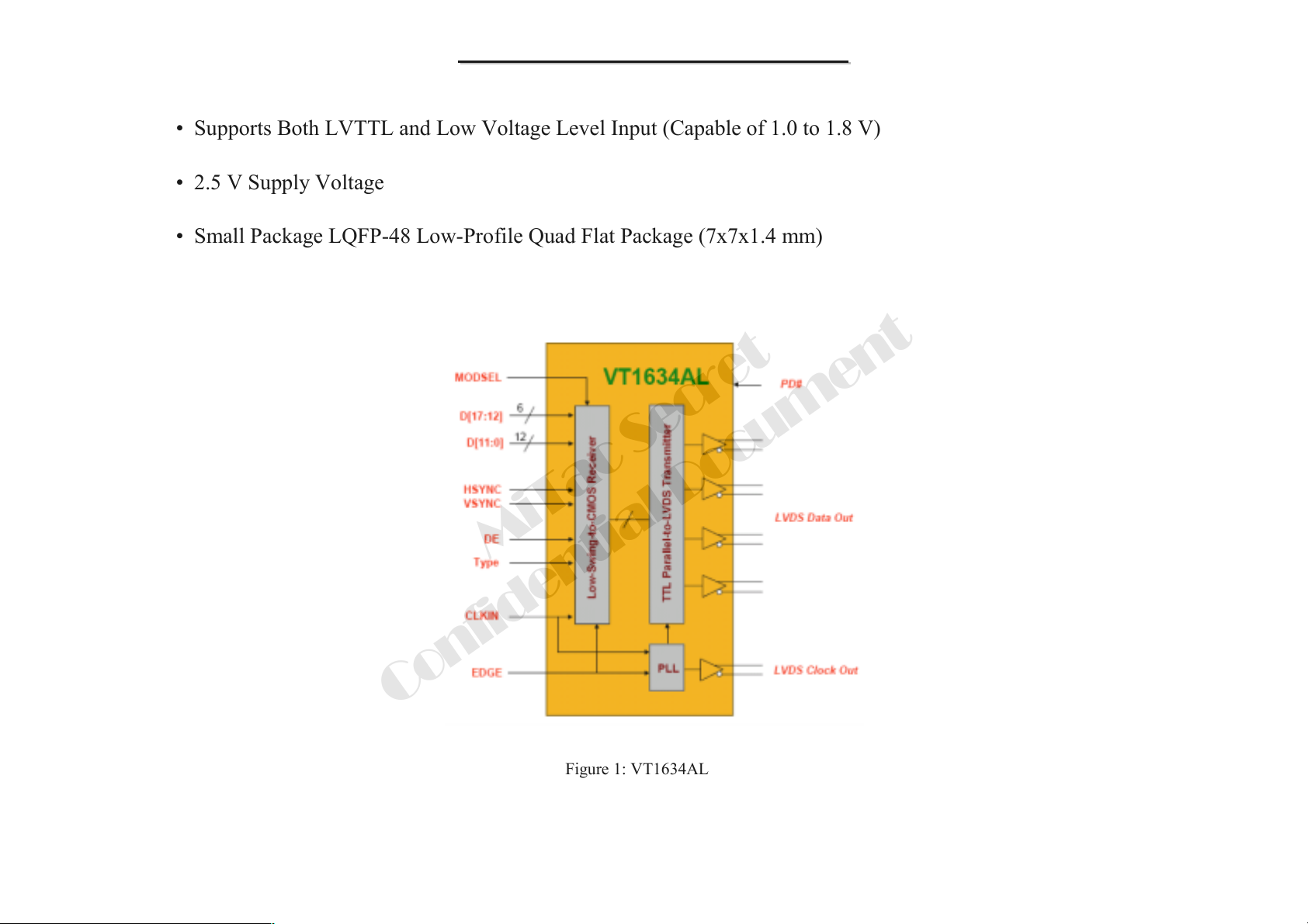
1.2.5 LVDS Transmitter: VT1634AL
MiTac Secret
The VT1634AL LVDS (Low Voltage Differential Signaling) transmitter is designed to support pixel data
transmission from a Host to Flat Panel Display ranging from VGA to WXGA resolutions. The transmitter converts
24-bit of CMOS/TTL input data into 4 LVDS (Low Voltage Differential Signaling) output data streams. With an
input clock at 85 MHz, the maximum transmission rate of each LVDS line is 595 Mbps, for an aggregate
throughput rate of 2.38 Gbps. A phase-locked transmit clock is transmitted in parallel with the output data streams
over the 4-channel LVDS link. The VT1634AL is designed to be compatible with Graphics Memory Controller
Hub by implementing two data per clock .Two input modes are supported: one port of 12-bit (two data per clock)
input for 24-bit RGB. In this mode, input data will be clocked on both rising and falling edges in LVTTL level
operation, or clocked on the cross over of differential clock signals in the low swing operation. Each input data
width will be 1/2 of clock cycle. The other mode is 18-bit input for 18-bit RGB.The VT1634AL is an ideal solution
to solve EMI and cable size problems for high-resolution flat panel display applications. The VT1634AL provides
Confidential Document
16
8650 N/B Maintenance
8650 N/B Maintenance
a reliable industry standard interface based on LVDS technology that delivers the bandwidth needed for high
resolution panels while maximizing bit times, and keeping clock rates low to reduce EMI and shielding
requirements.
Product Features
• Compiles with open LDI specification for digital display interfaces
• Compatible with TIA/EIA-644 LVDS standard
• Supports input pixel clock from 25 MHz to 85 MHz
• Supports LVDS panel resolution from VGA through WXGA (1280x800/1280x768)
• Single channel LVDS transmitter function
• Supports 18-bit/24-bit panel type
• Supports 24-bit TFT LCD with Conventional or Non-Conventional Color Mappings
• Supports MSB/LSB color data mapping option for 24-bit panel
• Narrow Bus Reduces Cable Size and Cost
• PLL Requires No External Components
• Power Down (PD#) Mode control
Confidential Document
MiTac Secret
17
8650 N/B Maintenance
8650 N/B Maintenance
• Supports Both LVTTL and Low Voltage Level Input (Capable of 1.0 to 1.8 V)
• 2.5 V Supply Voltage
• Small Package LQFP-48 Low-Profile Quad Flat Package (7x7x1.4 mm)
MiTac Secret
Confidential Document
Figure 1: VT1634AL
18
8650 N/B Maintenance
8650 N/B Maintenance
1.2.6 CardBus: CB1410
Features
• 3.3 V operation with 5 V tolerant
• LFBGA 144-ball package
• Compliant with
- PCI Local Bus Specification, Revision 2.2
- PCI Bus Power Management Interface Specification, Revision 1.1
- PCI Mobile Design Guide, Version 1.1
- Advanced Configuration and Power Interface Specification, Revision 1.0
- PC 99 System Design Guide
- PC Card Standard 8.0
- Interrupt configuration
- Supports parallel PCI interrupts
- Supports parallel IRQ and parallel PCI interrupts
- Supports serialized IRQ and parallel PCI interrupts
- Supports serialized IRQ and PCI interrupts
Confidential Document
MiTac Secret
19
8650 N/B Maintenance
8650 N/B Maintenance
- Power Management Control Logic
- Supports CLKRUN# protocol
- Supports SUSPEND#
- Supports PCI PME# from D3, D2, D1 and D0
- Supports PCI PME# from D3Cold
- Supports D3STATE# (CB1410 only)
- Power switch interface
- CB1410 supports parallel 4 wire power switch interface
- Misc Control Logic
- Supports serial EEPROM interface
- Supports socket activity LED
- Supports 5 GPIOs and GPE#
- Supports standard zoomed video port
- Supports SPKROUT, CAUDIO and RIOUT#
- Supports PCI LOCK#
Confidential Document
MiTac Secret
20
8650 N/B Maintenance
8650 N/B Maintenance
1.2.7 AC’97 Audio System: Advance Logic, Inc, ALC655
The ALC655 is a 16-bit, full duplex AC'97 2.3 compatible six channels audio CODEC designed for PC multimedia
systems, including host/soft audio and AMR/CNR based designs. The ALC655 incorporates proprietary converter
technology to meet performance requirements on PC99/2001 systems. The ALC655 CODEC provides three pairs
of stereo outputs with 5-Bit volume controls, a mono output, and multiple stereo and mono inputs, along with
flexible mixing, gain and mute functions to provide a complete integrated audio solution for PCs. The digital
interface circuitry of the ALC655 CODEC operates from a 3.3 V power supply for use in notebook and PC
applications. The ALC655 integrates 50mW/20ohm headset audio amplifiers at Front-Out and Surr-Out, built-in
14.318M 24.576MHz PLL and PCBEEP generator, those can save BOM costs. The ALC655 also supports the
S/PDIF input and output function, which can offer easy connection of PCs to consumer electronic products, such as
AC3 decoder/speaker and mini disk devices. ALC655 supports host/soft audio from Intel ICHx chipsets as well as
audio controller based VIA/SIS/ALI/AMD/nVIDIA/ATI chipset. Bundled Windows series drivers (win nXP/ME/
2000/98/NT), EAX/Direct Sound 3D/I3DL2/A3D compatible sound effect utilities (supporting Karaoke, 26-kind
of environment sound emulation, 10-band equalizer), HRTF 3D positional audio and Sensaura™ 3D (optional)
provide an excellent entertainment package and game experience for PC users. Besides, ALC655 includes
Realtek’s impedance sensing techniques that makes device load on outputs and inputs can be detected.
• Meets performance requirements for audio on PC99/2001 systems
MiTac Secret
Confidential Document
• Meets Microsoft WHQL/WLP 2.0 audio requirements
• 16-bit Stereo full-duplex CODEC with 48 KHz sampling rate
• Compliant with AC’97 2.3 specifications
21
8650 N/B Maintenance
8650 N/B Maintenance
- 14.318 MHz-24.576 MHz PLL to save crystal
- 12.288 MHz BITCLK input can be consumed
- Integrated PCBEEP generator to save buzzer
- Interrupt capability
- Three analog line-level stereo inputs with 5-bit
• Volume control: Line_In, CD, AUX
• High quality differential CD input
• Two analog line-level mono input: PCBEEP
• Phone-In
MiTac Secret
• Two software selectable MIC inputs
• Applications (software selectable)
• Boost preamplifier for MIC input
Confidential Document
• 50 mW/20 amplifier
• External Amplifier Power Down (EAPD) capability
• Power management and enhanced power saving features
22
8650 N/B Maintenance
8650 N/B Maintenance
• Stereo MIC record for AEC/BF application
• Supports power off CD function
• Adjustable VREFOUT control supports double sampling rate (96 KHz) of DVD audio playback
• Support 48 KHz of SPDIF output is compliant with AC’97 rev2.3 specification
• Power support: Digital: 3.3 V; Analog: 3.3 V/5 V
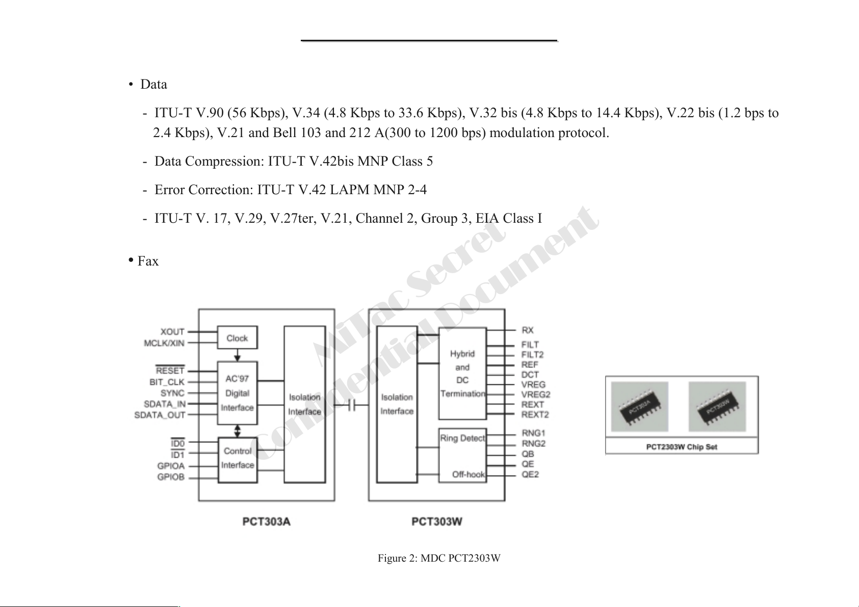
1.2.8 MDC: PC-TEL Modem Daughter Card PCT2303W (Askey V1456VQL-P1)
The PCT2303W chipset is designed to meet the demand of this emerging worldwide AMR/MDC market. The
combination of PC-TEL’s well proven PCT2303W chipset and the HSP56TM MR software modem driver allows
systems manufactures to implement modem functions in PCs at a lower bill of materials (BOM) while maintaining
higher system performance.
PC-TEL has streamlined the traditional modem into the Host Signal Processing (HSP) solution. Operating with the
Pentium class processors, HSP becomes part of the host computer’s system software. It requires less power to
operate and less physical space than standard modem solutions. PC-TEL’s HSP modem is an easily integrated,
cost-effective communications solution that is flexible enough to carry you into the future.
The PCT2303W chipset is an integrated direct access arrangement (DAA) and Codec that provides a
programmable line interface to meet international telephone line requirements. The PCT2303W chip set is
available in two 16-pin small outline packages (AC’97 interface on PCT303A and phone-line interface on
Confidential Document
MiTac Secret
23
8650 N/B Maintenance
8650 N/B Maintenance
PCT303W). The chipset eliminates the need for an AFE, an isolation transformer, relays, opto-isolators, and 2-to 4-
wire hybrid. The PCT2303W chipset dramatically reduces the number of discrete components and cost required to
achieve compliance with international regulatory requirements. The PCT2303W complies with AC’97 Interface
specification Rev. 2.1.
The chipset is fully programmable to meet world-wide telephone line interface requirements including those
described by CTR21, NET4, JATE, FCC, and various country-specific PTT specifications. The programmable
parameters of the PCT2303W chipset include AC termination, DC termination, ringer impedance, and ringer
threshold. The PCT2303W chip set has been designed to meet stringent world-wide requirements for out-of-band
energy, billing-tone immunity, lightning surges, and safety requirements.
Features
• Virtual com port with a DTE throughout up to 460.8 Kbps
• G3 Fax compatible
• Auto dial and auto answer
• Ring detection
Codec/DAA Features
• AC97 2.1 compliant
Confidential Document
MiTac Secret
24
8650 N/B Maintenance
8650 N/B Maintenance
• 86dB dynamic range TX/RX paths
• 2-4-wire hybrid
• Integrated ring detector
• High voltage isolation of 4000 V
• Support for “Caller ID”
• Compliant with FCC Part68, CTR21, Net4 and JATE
• Low power standby
• Low profile SOIC package 16 pins 10x3x1.55 mm
• Low power consumption
• 10 mA @ 3.3 V operation
• 1 mA @ 3.3 V power down
MiTac Secret
Confidential Document
• Integrated modem codec
Standard Features
25
8650 N/B Maintenance
8650 N/B Maintenance
•Data
- ITU-T V.90 (56 Kbps), V.34 (4.8 Kbps to 33.6 Kbps), V.32 bis (4.8 Kbps to 14.4 Kbps), V.22 bis (1.2 bps to
2.4 Kbps), V.21 and Bell 103 and 212 A(300 to 1200 bps) modulation protocol.
- Data Compression: ITU-T V.42bis MNP Class 5
- Error Correction: ITU-T V.42 LAPM MNP 2-4
- ITU-T V. 17, V.29, V.27ter, V.21, Channel 2, Group 3, EIA Class I
• Fax
MiTac Secret
Confidential Document
Figure 2: MDC PCT2303W
26
8650 N/B Maintenance
8650 N/B Maintenance
1.2.9 System Flash Memory (BIOS)
• Firmware Hub for Intel® 810, 810E, 815, 815E,815EP, 820, 840, 850 Chipsets
• Flexible Erase Capability
- Uniform 4 KBytes Sectors
- Uniform 16 KBytes overlay blocks for SST49LF002A
- Uniform 64 KBytes overlay blocks for SST49LF004A
- Top boot block protection
- 16 KBytes for SST49LF002A
- 64 KBytes for SST49LF004A
MiTac Secret
- Chip-Erase for PP Mode
• Single 3.0-3.6 V Read and Write Operations
• Superior Reliability
Confidential Document
• Firmware Hub Hardware Interface Mode
- 5-signal communication interface supporting byte Read and Write
- 33 MHz clock frequency operation
- WP# and TBL# pins provide hardware write protect for entire chip and/or top Boot Block
27
8650 N/B Maintenance
8650 N/B Maintenance
- Block Locking Register for all blocks
- Standard SDP Command Set
- Data# Polling and Toggle Bit for End-of-Write detection
- 5 GPI pins for system design flexibility
- 4 ID pins for multi-chip selection
1.2.10 Memory System: 64 MB, 128 MB, 256 MB, 512 MB (x64) 200-Pin DDR
SDRAM SO-DIMMs
• JEDEC-standard 200-pin, small-outline, dual in-line memory module (SODIMM)
MiTac Secret
• Utilizes 200 Mb/s and 266 Mb/s DDR SDRAM components
• 64 MB (8 Megx64 [H]); 128 MB (16 Megx64, [H] and [HD]); 256 MB (32 Megx64 [HD]); 512 MB (64
Megx 64 [HD])
• VDD= VDDQ= +2.5 V ±0.2 V
• VDDSPD = +2.2 V to +5.5 V
• 2.5 V I/O (SSTL_2 compatible)
• Commands entered on each positive CK edge
Confidential Document
28
8650 N/B Maintenance
8650 N/B Maintenance
• DQS edge-aligned with data for Reads; center-aligned with data for Writes
• Internal, pipelined double data rate (DDR) architecture; two data accesses per clock cycle
• Bidirectional data strobe (DQS) transmitted/received with data—i.e., source-synchronous data capture
• Differential clock inputs (CK and CK# - can be multiple clocks, CK0/CK0#, CK1/CK1#, etc.)
• Four internal device banks for concurrent operation
• Selectable burst lengths: 2, 4, or 8
• Auto precharge option
• Auto Refresh and Self Refresh Modes
• 15.6 µs (MT4VDDT864H, MT8VDDT1664HD), 7.8125 µs (MT4VDDT1664H, MT8VDDT3264HD,
MT8VDDT6464HD) maximum average periodic refresh interval
• Serial Presence Detect (SPD) with EEPROM
• Fast data transfer rates PC2100 or PC1600
• Selectable READ CAS latency for maximum compatibility
• Gold-plated edge contacts
Confidential Document
MiTac Secret
29
 Loading...