

Page 1
Service
SR7300 /
N1B/U1B/K1G/N1G/U1G
Manual
SELECT
S ANDBY
POWER ON/STANDBY
SURROUND
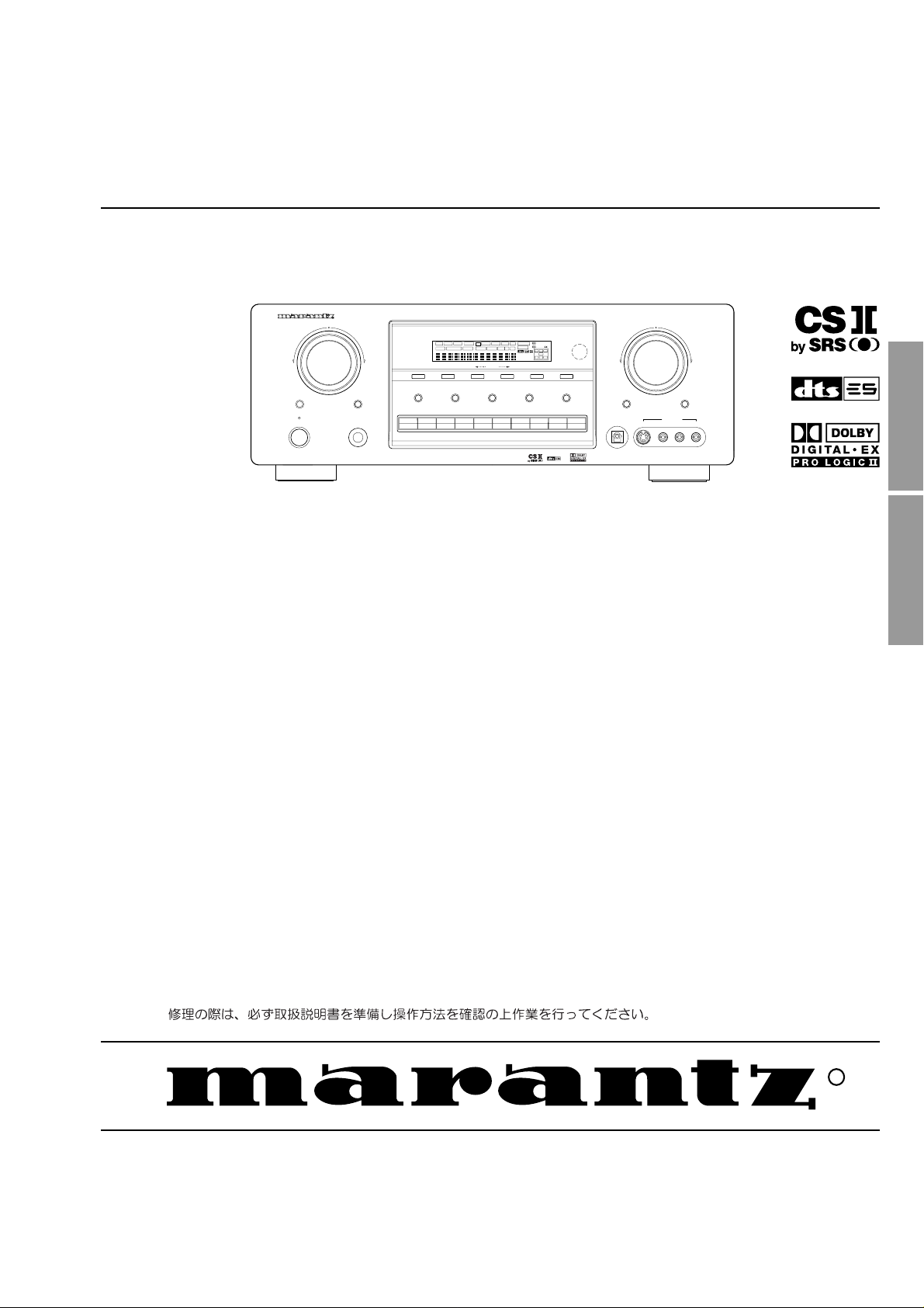
AV SURROUND RECEIVER SR7300
ENTER
PHONES
DSP MULI AUTO TUNED ST V OF NIGHT EAK ANA OG
SURR
AUTO
S EEP
MEMORY
CLEAR
VCR1
TV
DVD
DRECT DISC 61 MTX 61 SPKR AB EQ
DSSVCR2
AUX1 AUX2
SR7300F /
N1B/U1B/K1G/N1G/U1G
AV Surround Receiver
PS7300 /
F1B/F1N
AV Surround Amplifi er
VOLUME
URR UND
ATT
I IT L
DIGTAL
PCM
TUNING
AD71CH NPUTSPEAKRS A/B
F/P
SDI ECT MULTROOM
CDR
TAPE
MODE
CD
DOWN
TUNER
MUTE
SV DEODGI AL VID O L AUDIO R
UP
ATT
AUX1 NPUT
PS7300
TABLE OF CONTENTS
SECTION PAGE
1. TECHNICAL SPECIFICATIONS AND SERVICE TOOL........................................ 1
2. TECHNICAL DESCRIPTION................................................................................. 4
3. WIRING DIAGRAM................................................................................................ 5
4. BLOCK DIAGRAM................................................................................................. 7
5. SCHEMATIC DIAGRAM........................................................................................ 9
6. PARTS LOCATION .............................................................................................. 25
7. IC DATA................................................................................................................ 36
8. EXPLODED VIEW AND PARTS LIST ................................................................. 47
9. SERVICE PROGRAM.......................................................................................... 51
10. UPDATE FIRMWARE .......................................................................................... 53
11. POWER AMPLIFIER ADJUSTMENT .................................................................. 55
12. SYSTEM ERROR................................................................................................ 56
13. TR OUBLE SHOOTING........................................................................................ 57
14. ELECTRICAL PARTS LIST ................................................................................. 61
Please use this service manual with referring to the user guide ( D.F.U. ) without fail.
SR7300 / SR7300F
R
SR7300 / SR7300OSE / PS7300
03AJ855010 MIT
First Issue 2002.11
Page 2
MARANTZ DESIGN AND SERVICE
Using superior design and selected high grade components,
Only original
MARANTZ
parts can insure that your
MARANTZ
MARANTZ
product will continue to perform to the specifi cations for which
company has created the ultimate in stereo sound.
it is famous.
Parts for your
MARANTZ
ORDERING PARTS :
equipment are generally available to our National Marantz Subsidiary or Agent.
Parts can be ordered either by mail or by Fax.. In both cases, the correct part number has to be specifi ed.
The following information must be supplied to eliminate delays in processing your order :
1. Complete address
2. Complete part numbers and quantities required
3. Description of parts
4. Model number for which part is required
5. Way of shipment
6. Signature : any order form or Fax. must be signed, otherwise such part order will be considered as null and void.
USA
MARANTZ AMERICA, INC
1100 MAPLEWOOD DRIVE
ITASCA, IL. 60143
USA
PHONE : 630 - 741 - 0300
FAX : 630 - 741 - 0301
AMERICAS
SUPERSCOPE TECHNOLOGIES, INC.
MARANTZ PROFESSIONAL PRODUCTS
2640 WHITE OAK CIRCLE, SUITE A
AURORA, ILLINOIS 60504 USA
PHONE : 630 - 820 - 4800
FAX : 630 - 820 - 8103
EUROPE / TRADING
MARANTZ EUROPE B.V.
P. O. BOX 8744, BUILDING SILVERPOINT
BEEMDSTRAAT 11, 5653 MA EINDHOVEN
THE NETHERLANDS
PHONE : +31 - 40 - 2507844
FAX : +31 - 40 - 2507860
AUSTRALIA
TECHNICAL AUDIO GROUP PTY, LTD
558 DARLING STREET,
BALMAIN, NSW 2041,
AUSTRALIA
PHONE : 61 - 2 - 9810 - 5300
FAX : 61 - 2 - 9810 - 5355
CANADA
LENBROOK INDUSTRIES LIMITED
633 GRANITE COURT,
PICKERING, ONTARIO L1W 3K1
CANADA
PHONE : 905 - 831 - 6333
FAX : 905 - 831 - 6936
HONG KONG
Jolly ProAudio Broadcast Engineering Ltd.
UNIT 2, 10F, WAH HUNG CENTRE,
41 HUNG TO ROAD, KWUN TONG, KLN.,
HONG KONG
PHONE : 852 - 21913660
FAX : 852 - 21913990
AUSTRALIA
QualiFi Pty Ltd,
24 LIONEL ROAD,
MT. WAVERLEY VIC 3149
AUSTRALIA
PHONE : +61 - (0)3 - 9543 - 1522
FAX : +61 - (0)3 - 9543 - 3677
NEW ZEALAND
WILDASH AUDIO SYSTEMS NZ
14 MALVERN ROAD MT ALBERT
AUCKLAND NEW ZEALAND
PHONE : +64 - 9 - 8451958
FAX : +64 - 9 - 8463554
JAPAN
MARANTZ JAPAN, INC.
35- 1, 7- CHOME, SAGAMIONO
SAGAMIHARA - SHI, KANAGAWA
JAPAN 228-8505
PHONE : +81 42 748 1013
FAX : +81 42 741 9190
Technical
THAILAND
MRZ STANDARD CO., LTD
746 - 754 MAHACHAI ROAD.,
WANGBURAPAPIROM, PHRANAKORN,
BANGKOK, 10200 THAILAND
PHONE : +66 - 2 - 222 9181
FAX : +66 - 2 - 224 6795
TAIWAN
PAI- YUING CO., LTD.
6 TH FL NO, 148 SUNG KIANG ROAD,
TAIPEI, 10429, TAIWAN R.O.C.
PHONE : +886 - 2 - 25221304
FAX : +886 - 2 - 25630415
SHOCK, FIRE HAZARD SERVICE TEST :
SINGAPORE
WO KEE HONG DISTRIBUTION PTE LTD
130 JOO SENG ROAD
#03-02 OLIVINE BUILDING
SINGAPORE 368357
PHONE : +65 6858 5535 / +65 6381 8621
FAX : +65 6858 6078
MALAYSIA
WO KEE HONG ELECTRONICS SDN. BHD.
2ND FLOOR BANGUNAN INFINITE CENTRE
LOT 1, JALAN 13/6, 46200 PETALING JAYA
SELANGOR DARUL EHSAN, MALAYSIA
PHONE : +60 - 3 - 7954 8088
FAX : +60 - 3 - 7954 7088
KOREA
MK ENTERPRISES LTD.
ROOM 604/605, ELECTRO-OFFICETEL, 16-58,
3GA, HANGANG-RO, YONGSAN-KU, SEOUL
KOREA
PHONE : +822 - 3232 - 155
FAX : +822 - 3232 - 154
CAUTION : After servicing this appliance and prior to returning to customer, measure the resistance between either primary AC
cord connector pins ( with unit NOT connected to AC mains and its Power switch ON ), and the face or Front Panel of product and
controls and chassis bottom.
Any resistance measurement less than 1 Megohms should cause unit to be repaired or corrected before A C po wer is applied, and
verifi ed before it is return to the user/customer.
Ref. UL Standard No. 1492.
In case of diffi culties, do not hesitate to contact the Technical
Department at above mentioned address.
020816MIT
Page 3

1. TECHNICAL SPECIFICATIONS AND SERVICE TOOL
TECHNICAL SPECIFICATIONS
FM TUNER SECTION (SR ONLY)
Frequency Range .....................................87.5 - 108.0 MHz
Usable Sensitivity .................................IHF 1.8 µV/16.4 dBf
Signal to Noise Ratio ....................... Mono/Stereo 76/72 dB
Distortion......................................... Mono/Stereo 0.2/0.3 %
Stereo Separation.............................................1 kHz 45 dB
Alternate Channel Selectivity.....................± 300 kHz 60 dB
Image Rejection............................................ 98 MHz 70 dB
Tuner Output Level........1 kHz, ± 40 kHz Dev 800 mV(/K/N)
...........1 kHz, ± 75 kHz Dev 800 mV(/U)
AM TUNER SECTION (SR ONLY)
Frequency Range ............................. 531 - 1602 kHz (/K/N)
Frequency Range .................................520 - 1710 kHz (/U)
Signal to Noise Ratio ..................................................50 dB
Usable Sensitivity.............................................Loop 400 µV
Distortion........................... 400 Hz, 30 % Mod. 0.5 % (/K/N)
.................................1 kHz, 30 % Mod. 0.5 % (/U)
Selectivity.......................................... ± 18 kHz 70 dB (/K/N)
..............................................± 20 kHz 70 dB (/U)
AUDIO SECTION
Power Output (20 Hz - 20 kHz/THD=0.08%)
Front L&R...............................................8 ohms 105 W / Ch
Center....................................................8 ohms 105 W / Ch
Surround L&R........................................8 ohms 105 W / Ch
Surround Back.......................................8 ohms 105 W / Ch
Front L&R...............................................6 ohms 130 W / Ch
Center....................................................6 ohms 130 W / Ch
Surround L&R........................................6 ohms 130 W / Ch
Surround Back.......................................6 ohms 130 W / Ch
Input Sensitivity/Impedance................... 168 mV/ 47 kohms
Signal to Noise Ratio(Analog Input / Source Direct) 105 dB
Frequency Response
Analog Input / Source Direct.....8 Hz - 100 kHz (± 3 dB)
Digital Input / 96 kHz PCM......... 8 Hz - 45 kHz (± 3 dB)
VIDEO
Television Format............................................. NTSC (/F/U)
......................................NTSC/PAL (/K/N)
Input Level/Impedance................................1 Vp-p/75 ohms
Output Level/Impedance.............................1 Vp-p/75 ohms
..............5 Hz to 8 MHz (– 1 dB) (/U)
Component Video Frequency Response. 5 Hz to 40 MHz (– 3 dB) (/K/N)
S/N.............................................................................60 dB
GENERAL
Power Requirement........................AC 100 V 50/60 Hz (/F)
......................... AC 230 V 50 Hz (/K/N)
.............................AC 120 V 60 Hz (/U)
Power Consumption...................................................480 W
Weight........................................28.9 lbs (13.1 Kg) (/K/N/U)
...............................................................14.7 Kg (/F)
ACCESSORIES
Remote Control Unit
RC7300SR................................................................... 1
AA-size batteries............................................................... 2
FM Antenna (SR ONLY)..................................................... 1
AM Loop Antenna (SR ONLY) ...........................................1
AC Cable...............................................................1 (/F/K/N)
Specifi cations subject to change without prior notice.
Video Frequency Response
........5 Hz to 10 MHz (– 3 dB) (/K/N)
SERVICE T OOL
Updated of the CPU and DSP DISC ........................... *SR7300CDR
(The disc is regarding when exchanged in QU01.)
1
Page 4
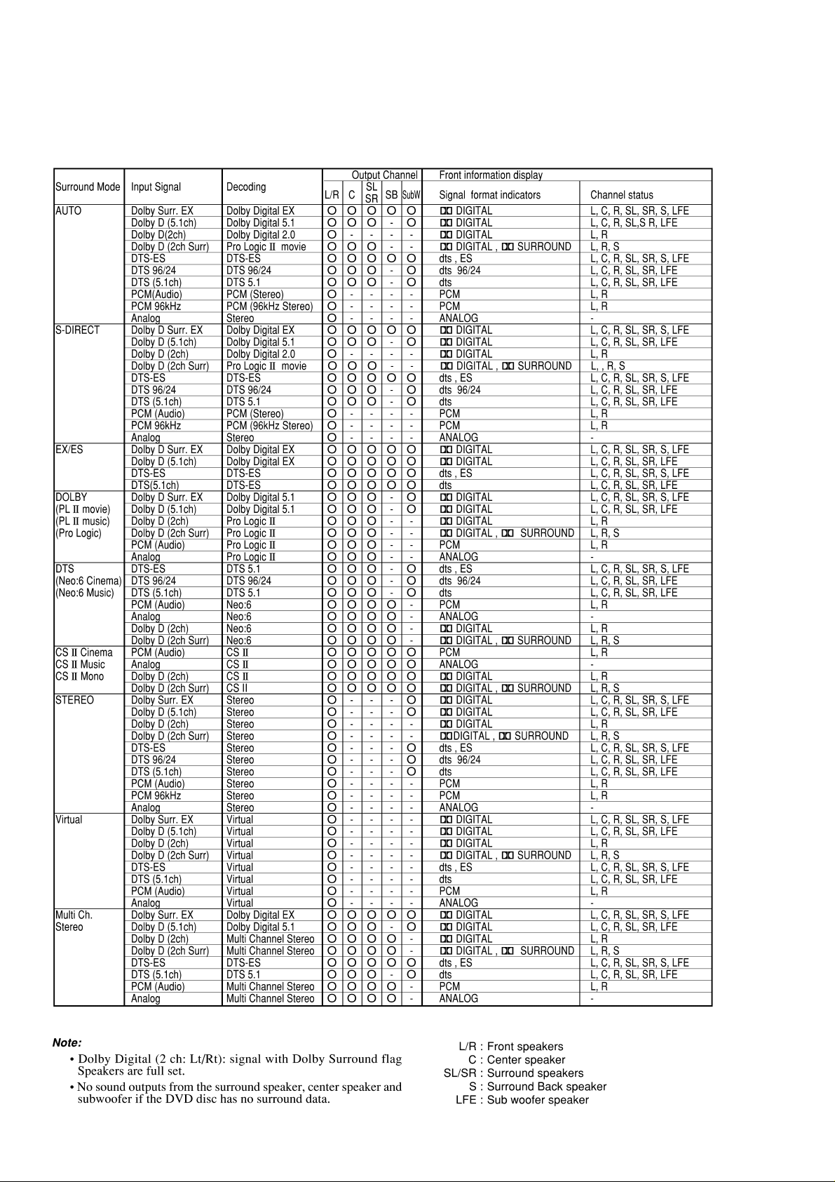
The relation between the selected surround mode and the input signal
The surround mode is selected with the surround mode buttons on SR7300/SR7300F/PS7300 or the remote control unit.
However, the sound you hear is subject to the relationship between the selected surround mode and input signal. That
relationship is as follows;
2
Page 5
Remark : Bass signal output from Sub Woofer terminal for SR7300 / SR7300F / PS7300
*Stereo decode : SPK SETUP - BASS MIX : BOTH set
SPK setup SubWoofer Output by Decoded mode
Sub
Woofer L/R (L/R) DTS mES,dES DTS, DTS96/24
None No output
Front Center
Yes Large Large Large Large LFE LFE none L+R L+R no output
Small Large Large LFE+C LFE+C C L+R L+R no output
None Large Large LFE LFE none L+R L+R no output
Small Large Large Large LFE+L+R LFE+L+R L+R L+R L+R no output
Small Large Large LFE+L+R+C LFE+L+R+C L+R+C L+R L+R no output
None Large Large LFE+L+R LFE+L+R L+R L+R L+R no output
Surr.
Surr.B DD EX Dolby(AC-3 2ch)
Small LFE+Sb
None no suuround mode
Small Large LFE+SL+SR LFE+SL+SR
Small LFE+SL+SR+Sb
None no suuround mode
None (prohibit) no suuround mode LFE
Small LFE+C+Sb
None no suuround mode
Small Large LFE+C+SL+SR LFE+C+SL+SR
Small LFE+C+SL+SR+Sb
None no suuround mode
None (prohibit) no suuround mode LFE+C
Small LFE+Sb
None no suuround mode
Small Large LFE+SL+SR LFE+SL+SR
Small LFE+SL+SR+Sb
None no suuround mode
None (prohibit) no suuround mode LFE
Small LFE+L+R+Sb
None no suuround mode
Small Large LFE+L+R+SL+SR LFE+L+R+SL+SR
Small LFE+L+R+SL+SR+Sb
None no suuround mode
None (prohibit) no suuround mode LFE+L+R
Small LFE+L+R+C+Sb
None no suuround mode
Small Large LFE+L+R+C+SL+SR LFE+L+R+C+SL+SR
Small LFE+L+R+C+SL+SR+Sb
None no suuround mode
None (prohibit) no suuround mode LFE+L+R+C
Small LFE+L+R+Sb
None no suuround mode
Small Large LFE+L+R+SL+SR LFE+L+R+SL+SR
Small LFE+L+R+SL+SR+Sb
None no suuround mode
None (prohibit) no suuround mode LFE+L+R
PL ,Neo6 CS
Stereo Virtual
(PCM:Auto )
(Main spk L fix)
3
Page 6
2. TECHNICAL DESCRIPTION
DTS was introduced in 1994 to provide 5.1 channels of discrete
digital audio into home theater systems.
DTS brings you premium quality discrete multi-channel digital sound
to both movies and music.
DTS is a multi-channel sound system designed to create full range
digital sound reproduction.
The no compromise DTS digital process sets the standard of quality
for cinema sound by delivering an exact copy of the studio master
recordings to neighborhood and home theaters.
Now, every moviegoer can hear the sound exactly as the moviemaker intended.
DTS can be enjoyed in the home for either movies or music on of
DVD’s, LD’s, and CD’s.
“DTS” and “DTS Digital Surround” are registered trademarks of Digital Theater Systems, Inc.
The advantages of discrete multichannel systems over matrix are
well known.
But even in homes equipped for discrete multichannel, there
remains a need for high-quality matrix decoding. This is because of
the large library of matrix surround motion pictures available on disc
and on VHS tape; and analog television broadcasts.
The typical matrix decoder of today derives a center channel and
a mono surround channel from two-channel matrix stereo material.
It is better than a simple matrix in that it includes steering logic to
improve separation, but because of its mono, band-limited surround
it can be disappointing to users accustomed to discrete multichannel.
Neo 6 offers several important improvements as follow,
. Neo 6 provides up to six full-band channels of matrix decoding
from stereo matrix material. Users with 6.1 and 5.1 systems will
derive six and fi ve separate channels, respectively, corresponding to
the standard home-theater speaker layouts.
. Neo 6 technology allows various sound elements within a channel
or channels to be steered separately, and in a way which follows
naturally from the original presentation.
. Neo 6 offers a music mode to expand stereo nonmatrix recordings
into the fi ve- or six-channel layout, in a way which does not diminish
the subtlety and integrity of the original stereo recording.
DTS-ES Extended Surround is a new multi-channel digital signal
format developed by Digital Theater Systems Inc. While offering high
compatibility with the conventional DTS Digital Surround format,
DTSES Extended Surround greatly improves the 360-degree surround impression and space expression thanks to further expanded
surround signals. This format has been used professionally in movie
theaters since 1999.
In addition to the 5.1 surround channels (FL, FR, C, SL, SR and
LFE), DTS-ES Extended Surround also offers the SB (Surround
Back) channel for surround playback with a total of 6.1 channels.
DTS-ES Extended Surround includes two signal formats with different surround signal recording methods, as DTS-ES Discrete 6.1 and
DTSES Matrix 6.1.
“DTS”, “DTS-ES Extended Surround” and “Neo:6” are trademarks of
Digital Theater Systems, Inc.
more favorable aural characteristics.
DTS 96/24 allows for 5.1channel sound tracks to be encoded at a
rate of 96kHz/24bits on DVD-Video titles.
When DVD-video appeared, it became possible to deliver 24-bit, 96
kHz audio into the home, but only in two channels, and with serious
limitations on picture. This capability has had little use.
DVD-audio allows 96/24 in six channels, but a new player is needed,
and only analog outputs are provided, necessitating the use of the
D/A converters and analog electronics provided in the player.
DTS 96/24 offers the following:
1.Sound quality transparent to the original 96/24 master.
2.Full backward compatibility with all existing decoders. (Existing
decoders will output a 48 kHz signal)
3.No new player required: DTS 96/24 can be carried on DVD-video,
or in the video zone of DVD-audio, accessible to all DVD players.
4.96/24 5.1-channel sound with full-quality full-motion video, for
music programs and motion picture soundtracks on DVD-video.
Dolby Digital identifi es the use of Dolby Digital (AC-3) audio coding
for such consumer formats as DVD and DTV. As with fi lm sound,
Dolby Digital can provide up to fi ve full-range channels for left,
center, and right screen channels, independent left and right surround channels, and a sixth ( “.1”) channel for low-frequency effects.
Dolby Surround Pro Logic II is an improved matrix decoding technology that provides better spatiality and directionality on Dolby Surround program material; provides a convincing three-dimensional
soundfi eld on conventional stereo music recordings; and is ideally
suited to bring the surround experience to automotive sound. While
conventional surround programming is fully compatible with Dolby
Surround Pro Logic II decoders, soundtracks will be able to be
encoded specifi cally to take full advantage of Pro Logic II playback,
including separate left and right surround channels. (Such material
is also compatible with conventional Pro Logic decoders.)
Dolby Digital EX creates six full-bandwidth output channels from
5.1- channel sources. This is done using a matrix decoder that
derives three surround channels from the two in the original recording. For best results, Dolby Digital EX should be used with movies
soundtracks recorded with Dolby Digital Surround EX.
Manufactured under license from Dolby Laboratories. “Dolby”, “Pro
Logic”, and the double-D symbol are trademarks of Dolby Laboratories.
Circle Surround II (CS-II) is a powerful and versatile multi-channel
technology. CS-II is designed to enable up to 6.1 multi-channel surround sound playback from mono, stereo, CS encoded sources and
other matrix encoded sources. In all cases the decoder extends
it into 6 channels of surround audio and a LFE/subwoofer signal.
The CS-II decoder creates a listening environment that places the
listener “inside” music performances and dramatically improves both
hi-fi audio conventional surround-encoded video material. CS-II
provides composite stereo rear channels to greatly improve separation and image positioning adding a heightened sense of realism
to both audio and A/V productions.
CS-II is packed with other useful feature like dialog clarity (SRS
Dialog) for movies and cinema-like bass enrichment (TruBass).
CS-II can enable the dialog to become clearer and more discernable in movies and it enables the bass frequencies contained in
the original programming to more closely achieve low frequencies
overcoming the low frequency limitations of the speakers by full
octave.
SRS Circle Surround II, SRS Dialog, SRS TruBass, SRS and
symbol
SRS Circle Surround II, SRS Dialog and SRS TruBass technology
are incorporated under license from SRS Labs, Inc.
are trademarks of SRS Labs, Inc.
The stereo CD is a 16-bit medium with sampling at 44.1 kHz. Professional audio has been 20- or 24-bit for some time, and there is
increasing interest in higher sampling rates both for recording and
for delivery into the home. Greater bit depths provide extended
dynamic range. Higher sampling rates allow wider frequency
response and the use of anti-alias and reconstruction fi lters with
4
Page 7
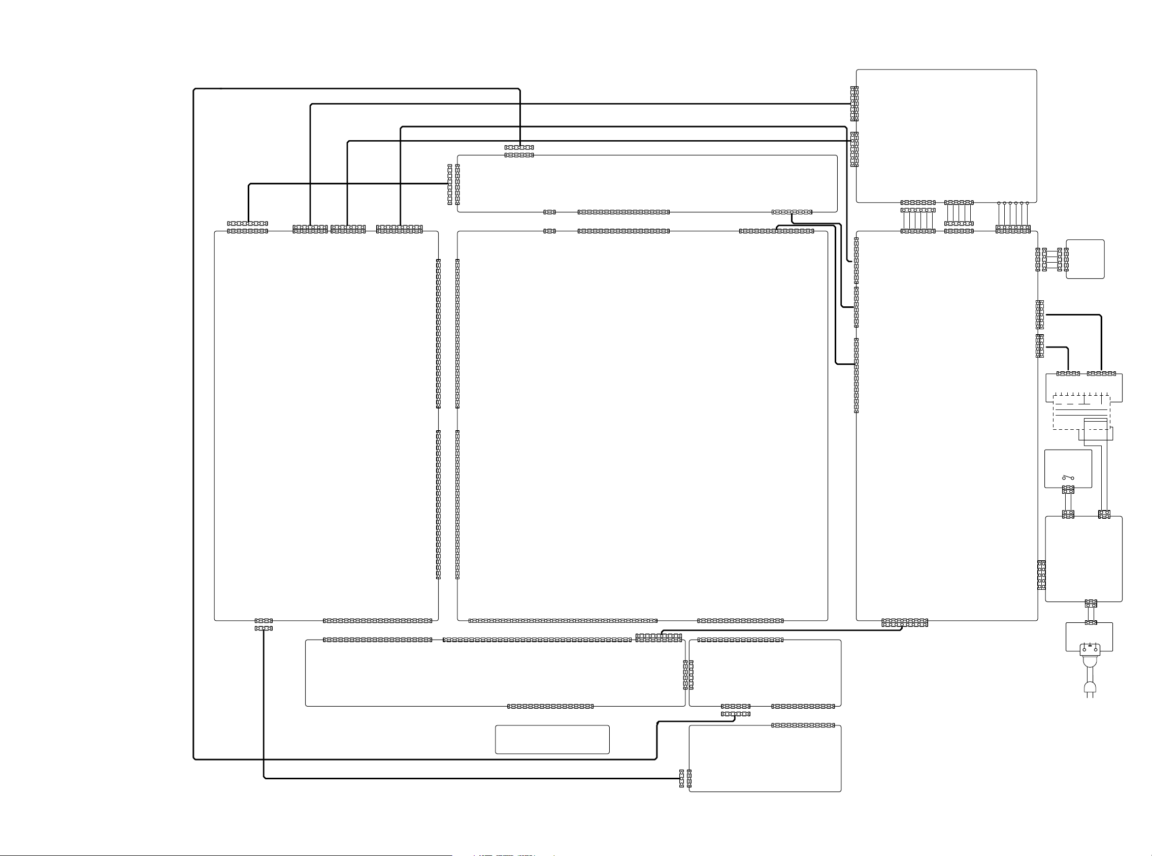
3. WIRING DIAGRAM
3
2
AGND
+12V1AUXR
JS06
07-FMN-BTK-A
YJ07022210
JE11
B3B EH
YP0600383X
ONLY F
WP03
6
AUXL5DGND4-12V
TU_L2GND3TU_R
1
7
N.C
Function/Vol PCB
JE08
B6B EH
YP0600384X
PS04
6GND
5FR
J101
4GND
B6B P H
YJ06006260
3SL
2GND
1FL
GND
WC01
9
GND8TXD
6
SBL
5
GND
4
CNT
3
GND
2
SR
1
J102
B6B EH
YP0600384X
J805
B6P VH
YP0600369 0
1
+12V
2
+12VG
3
12V
W808
4
BOAD N
+5VD
YB00700930
5
+5VDG
6
+5VV
7
+5VVG
8
+5VL
1
FL2
2
FL1
3
VKK
4
J803
GND
B7B PH
5
GND
YJ06006270
6
+5VD
7
+5VL
13
HP ON
12
HP DET
11
P DOWN
10
STANDBY
HEAT DET
9
8
P L NE FAIL
7
P AMP FAIL
6
N C
5
HEAT
4
SURR ON
3
FLRB ON
2
FLRA ON
1
N C
J810
13FMN BTK A
YJ07060300
J809
B8B PH
YJ06006280
+12V
2
1
W809
GND2+5VV3GND4TXD5-5VV6RTS7COMP_SEL
1
10
11
GND
+5VV
WP02
1
2
3
4
5
JP02
S5B PH
GND
GND
7
AUXR
6
+12V
5
GND
JP03
4
12V
07 FMN SSTK A
YJ07060420
3
DGND
2
AUXL
1
+5VD
1
MAIN_FL
19
1
WG02
1
7
8
2
3
4
5
6
GND
GND
GND
MAIN_SBL
JE09
B6B PH
YJ06006260
TU_R
5SW4
3
2
GND
GND
TU_L
TU_R
MA N_CEN
+5VL
+5VVG
MA N_SR
JS05
B8B PH
YJ06006280
JE10
19FMN BTK A
YJ07059880
WG04
11
10
9
8
7
6
SBL
SBR
CNT
GND
GND
GND
J972
19FMN BTK A
YJ07059880
1
2
3
4
5
6
NC
-12V
+12V
+5VD
+12VG
+5VDG
1CE VOLB
1 CE VOLB
2CE VOLA
2 CE VOLA
3VOLCLK
3 VOLCLK
4VOLDATA
4 VOLDATA
5GND
5GND
6GND
6GND
JS11
TKC W26P C1
YJ06004170
JS13
TKC W26P C1
YJ06004170
15SL14
13SR12
GND
GND
GND
SL SRMUTE
18
17FR16
FL2GND3FR4GND5SL6GND7SR8GND9SBL10GND11SBR12GND13CNT14GND15SW16GND17TU_L18GND
1
19
FL
GND
33FMN BTK A
YJ07060310
7GND
8+5VD
9+5VD
10+5VD
11GND
12GND
13+5VL
14L/RMUTE
15
16SBMUTE
17CNTMUTE
18SWMUTE
19MULTIMUTE
20ERMUTE
21P DOWN
22CE TCB
23CE TCA
24AFCLK
25AFDATA
26+5VL
1SL
2SL+
3GND
4SR+
5SR
6SBL
7SBL+
8GND
9SBR+
10SBR
11CEN
12CEN+
13GND
14GND
15FR
16FR+
17GND
18FL+
19FL
2012V
21RT
21 RT
22GND
23LT
24GND
25SW+
26SW
32
33
M_RC_OUT
JA08
7GND
8 +5VD
9 +5VD
10 +5VD
11 GND
12 GND
13 +5VL
14 L/RMUTE
15 SLSRMUTE
16 SBMUTE
17 CNTMUTE
18 SWMUTE
19 MULTIMUTE
20 ERMUTE
21 P DOWN
22 CE TCB
23 CE TCA
24 AFCLK
25 AFDATA
26 +5VL
1SL
2SL+
3GND
4SR+
5SR
6 SBL
7 SBL+
8GND
9 SBR+
10 SBR
11 CEN
12 CEN+
13 GND
14 GND
15 FR
16 FR+
17 GND
18 FL+
19 FL
20 12V
22 GND
23 LT
24 GND
25 SW+
26 SW
29
30
31
R
RC_OUT
M_RC_IN
TKC W26X A1
YP0700562Y
JU01
TKC W26X A1
YP0700562Y
M_RC_OUT
M_RC_IN
2
1
27
28
DC_OUT1
RC_IN
JU02
RC_OUT
3
26
DC_OUT2
DC_OUT1
RC_IN
IR
7
6
5
4
25
D G_OUT
MD2
WG01
2
3
4
5
6
GND
GND
GND
MAIN_SL
MA N_FR
Dig IN/OUT, RC-5 ,Preout PCB
PD04
AUX1_Y
DC_OUT2
8
22
D G1_ N23D G1_ N24D G_OUT
AUX1_C
B2B PH SM3 TB
YJ0701972Y
DIG_OUT
MD2
9
20
21
D G2_ N
D G2_ N
JP01
S2B PH
YJ06006420
JU07
18
19
D G3_ N
YJ06006450
AUX1_CVBS
WP01
DIG2_IN
DIG1_IN11DIG1_IN10DIG_OUT
14
13
12
16
17
D G4_ N
D G4_ N
D G3_ N
WG05
tuner pack
AUX_OPT
1
1
AUX_OPT
DIG2_IN
15
15
D G5_ N
Vcc2(+5V)10FM FOUT11GND12DO13CLK14DI15CE
9
GND
2
2
GND
DIG3_IN
14
16
D G5_ N
W602
DIG3_IN
17
DIG4_IN
18
DIG4_IN
19
DIG5_IN
20
1
GND
DIG5_IN
PC04
Front PCB
WC01
11
10
9
8
7
6
5
4
3
KEY0
VOL-
VOL+
_RSFL
RCOUT
SIOCLK
_CEFLD2_RSTFL
S ODATA
_S.BYLED
P604
CPU/DSP/DAC/ADC PCB
KILL_RDS
CE_TU26TU_MUTE25TU_ST24TU_SD23DIG_GND22DIG6_IN21DIG6_IN
_CE_RDS
29
28
27
1
RDSDIN2TUDIN3TUCLK4TUDOUT5_CE_RDS6KILL_RDS7CE_TU8TU_MUTE9TU_ST10TU_SD11D G_GND12D G6_ N13D G6_ N
YJ06006280
JT01
15FE BT VK N
YJ07020480
STEREO2TUNED3MUTE4R_OUT5GND6L_OUT7DETOUT8Vcc1(+12V)
OTHER F
1
+5VL
B8B PH
12
J980
_WR T
+5VVG
33
+5VV
16FMN SSTK A
SEL-2KEY23SEL+4KEY15_WRIT6KEY07_S.BYLED8_RSFL9VOL-10SIODATA11VOL+12SIOCLK13RCOUT14_CEFLD15_RSTFL16GND
YJ07060510
1
16
SEL-15KEY214SEL+13KEY1
JU06
33FMN BMT A TFT
YJ0702683Z
RDSD N32TUD N31TUCLK30TUDOUT
-12V
+5VD
+5VDG
J981
B5B EH
YP0601045X
WF01
JC03
JU03
16FMN BMTR A TFT
YJ0702703Z
12345678
+12V
+12VG
5 +5VL
+5VL
4 GND
GND
3 12V
12V
2 GND
GND
1 +5VV
+5VV
WG06
1 TU L
2 GND
3 TU R
GND
OSDCLK
VSYNC
OSDDATA
4
3
2
1
12
13
14
15
GND
VSYNC
OSDCLK
OSDDATA
JL07
S5B EH
YP06003950
JL04
S5B PH
YJ06006450
WP02
Component Video PCB
JS72
S3B-EH
YP06003930
ONLY F
JC02
S7B PH
YJ06006470
1
2
4
5
HP_ON
_HP_DET3_P_DOWN
JU04
TV_AUTO
7
6
9
TV_AUTO
CVBS_OSD
TXD
8
8
TXD
CVBS_OSD
9
7
Y_OSD
Y_OSD
_STANDBY
RTS
RXD11_CEEX
12
10
4
5
6
RTS
RXD
_CEEX
13FMN BMT A TFT
YJ0702663Z
_CEOSD
5
10
11
_CEOSD
Composite/S-Video PCB
JL06
11FMN BTK A
AUX1_CVBS
AUX1_Y
AUX1_C
GND
GND
YJ07060290
2
3
4
5
1
JF54
11FMN BTK A
YJ07060290
6
7
_HEAT_DET
_P_LINE_FA L
N.C
14
13
2
3
N.C
CTS
CTS
WC02
P_AMP_FA L
15
10
8
N.C
GND
W601
1
GND
CTS11GND
2
CTS1GND
9
10
HEAT
SURR_ON11FLRB_ON12FLRA_ON
JU05
15FMN BMT A TFT
YJ0702665Z
JL05
15FMN BTK A
YJ07026120
PL04
RXD9_COMP_MUTE
8
WL01
6
5
4
3
RXD
COMP_SEL
_COMP_MUTE
PF04
+5VL6+5VD5GND4GND3VKK2FL11FL2
7
13
GND
7
RTS
-5VV
P104
Power AMP PCB
-B2-B
3AC4AC5+B6
1
4AC3AC2-B1
-B
W805
BOAD IN
YB00062800
P804
Power Supply PCB
-12V
+12VG
+5VD
+5VV
+5VDG
+5VVG
3
4
5
6
7
W806
BOAD N
YA03051820
5
HEAT_DET
4
PA_FA L
2
3
GND
-12V
J806
B5B EH
YP0601045X
+12V2GND3-12V4PA_FAIL5HEAT_DET
1
1
+12V
+B
6
+B5+B
YB00309410
SBL
B6P VH
YP06003690
4SR5C6
W179
J179
3
FR
YP0600391X
YP06010950
YP0600391X
123456
1
FL2SL
WP91
4HP L
3GND
2HP R
1HP DET
JP91 JP92
B4B EH
J801
B5P VH
AC BH
5
4
AC BL
3
CENTER
2
AC BL
1
AC BH
4
AC FL
3
AC FL
2
AC +5
1
AC +5
J802
B4B EH
W891
1234
BOAD IN
YB00067390
4 HPL
3GND
2 HPR
1 HP DET
B4B EH
P894
H.P PCB
PP94
YP0600391X
1234 5
P864
BOAD N
YA03040620
12345678910
1112
W861
W892
P884
PowerSW PCB
J881
21
B2P3 VH
YP04000760
12
W852
J852
B2P3 VH
YP04000760
12
J854
B2P3 VH
YP04000760
AC
AC
1
AC2AC
P854
BackUP PCB
1
1
P DOWN
P DOWN
2
2
STANDBY
STANDBY
3
PR POWER
3
RR POWER
4
+5VL
4
+5VL
5
5
GND
GND
J853J807
S5B XH
05JQ BT
YP06006410
YJ06008750
+5VL
8
W871
BOAD IN
AC Inlet PCB
J871
AC INLET
P874
N
2
YD020218E0
YD020218F0
12
L
YP0400076012
J851
B2P3 VH
5 6
Page 8
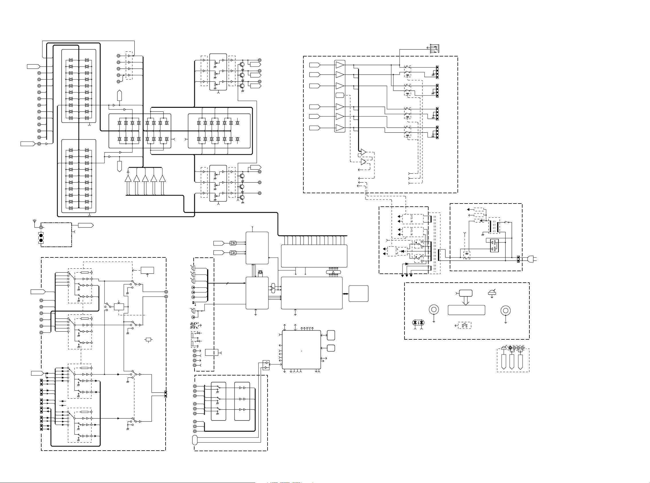
4. BLOCK DIAGRAM
M F L R
From Front AUX
AUX(L/R)
TV IN
DVD IN
VCR1 IN
VCR1 OU T
DSS/VCR2 IN
DSS/VCR2 OUT
CD IN
TAPE IN
TAPE OU T
CDR/MD IN
CDR/MD OUT
*TUNER IN
AUX CVBS
TV IN
From Front AUX
+6dB
TUNER
1
MODULE
2
DSS IN
TV N
VCR1 IN
VCR2 IN
AUX IN
DVD IN
VCR1 IN
VCR1 OUT
DSS IN
DSS OUT
AUX Y/C
From Front AUX
DVD IN +6 B
TV IN
VCR1 IN
VCR1 OUT
DSS IN
DSS OUT
AUX IN
TV N
DVD IN
VCR1 IN
DSS IN
AUX IN
TV IN
Y
DVD IN
VCR1 N
C
DSS IN
Y
C
Y
C
Y
C
LD N
C
TV N
Y
VCR1 IN
VCR2 IN
C
AUC IN
Y
C
TC9273 013
Function SW
(MULTI ROOM) (MA N )
INLA
M F LM F L
NLB
AUX L
AUX L
INLC
TV L
TV L
INLD
DVD L
DVD L
INLE
VCR1 L
VCR1 L
INLF
DSS L
DSS L
INLG
CD L
CD L
INLH
TAPE L
TAPE L
INLI
CDR LCDR L
INLJ
TUNER L TUNER L
TC9273 013
Function SW
(MULTI ROOM)
INLA INLA
M F R
M F R
NLB
AUX R
AUX R
INLC
TV R
TV R
INLD
DVD R
DVD R
INLE
VCR1 R VCR1 R
INLF
DSSR DSS R
INLG
CD RCD R
INLH
TAPE RTAPE R
INLI
CDR RCDR R
INLJ
TUNER RTUNER R
To Functon SEL
TUNER L/R
Tuner Cont
QL01
NJM2595
CONT
+6dB DRV
+6dB DRV
+6dB DRV
CONT
+6dB
+6dB
+6dB
NJM2595
MULTI ROOM SEL
QX02
NJM2595
CONT
+6 B
+6 B
Y Signal
C Signal
NJM2595
CONT
+6 B
+6 B DRV
+6 B
INLA
INLB
INLC
INLD
INLE
INLF
INLG
INLH
INLI
INLJ
Func. SW Cont
(MA N)
INLB
INLC
INLD
INLE
INLF
INLG
INLH
INLI
INLJ
CVBS SEL
DRV
DRV
DRV
QF01
DRV
DRV
DRV
QX01
DRV
DRV
Lch
Rch
Func SW Cont
VCR1 OUT
VCR2 OUT
VCR1 OUT(Y)
VCR2 OUT(Y)
Y SEL
VCR1 OUT(C)
VCR2 OUT(C)
C SEL
7 1ch IN
FRONT L/R
SURR L/R
SURR BACK L/R
CENTER
Sub Woofer
Function SW
T9164
INLA
INLA
BP
OSD
OSD Cont
OSD
LC74781
NJM2535
QL02
VCR1 OUCR1 OUT R
Rt to ADC
Lt to ADC
QL03
NLB INLB
*OPTION
DSS OUT LDSS OUT R
D SW
QX04
NJM2244
QX03
NJM2264
INLC
TAPE_OU _LTAPE_OUT_R
INLC
NJM2244
QL04
NJM2244
QF02
M SB L R
M CEN SW
INLD
INLD
ANA F R
D CNT
M F L R
M S L R
ANA F L
C R_OUT_R CDR_OUT_
DRV
DRV
DRV
DRV
FRONT LFRONT R
INLE
D_F_L
D_F_R
INLE
D SB L R
QL05, QF03
74HC4094 x2
S Register
VIDEO P EXP Cont
OSD/FL Cont
5V5V
1
Detect
Unbal
Detect
FL FL
Regula or
Regula or
STANDBY LED
_WRTI
PH DET
STANDBY
MAIN TRANSF
ROTARY ENCODER
(SURR MODE)
MOD ENC
FRONT L (A)
FRONT R (A)
FRONT L (B)
FRONT R (B)
CENTER
SURR BACK
SURROUND L
SURROUND R
OSD/FL Cont
KEY0 2
+5VL
P Down
S andby
QC01
FL DRIVER
NJU3430
FL DISPLAY
KEY MATRIX
12
+5VL Reg
Power Down
+9V
VC01
SUB TRANSF
34
AC OUTLETS
R SENSOR
RC-5 IN
POWER SW
1
ROTARY ENCODER
(MASTER VR)
VR ENC
D-AUX
Y/C
To V DEO(CVBS)
AUX CVBS
1
2
AUX L/R
To Functon
QE11
6CH E VR TC9499N
FRONT
SURR
SURR BACK
SURR L
Function SW
T9162
INLGINLG
INLH
INLF
M F L
ANA F L
M F R
ANA F R
INLF
INLH
Func SW Cont
D F L R
D S L R
INLA
D_S_L
D_S_R
INLA
CNT
SUB W
MULTI
INLBNLB
M_S_L
M_S_R
SURR R
*OPT ON
INLC
D SB L
D SB R
INLC
6CH E VR TC9499N
DIG 1
DIG 2
DIG 3
DIG 4
MONITOR
DIG 5
1
DIG 6
MULTI MONI
DIG AUX
OPT OUT
COAX OUT
Ver.Up
SW
23
DC OUT 1
DC OUT 2
RC-5 IN
RC-5 OUT
DC 1
DC 2
RDS
LC
MULTI RC IN
MULTI RC OUT
DVD Y
DVDY
DSS Y
DVD CB
DVD
Y
C
MONITOR 1 OUT
DSS
MONITOR
OUT
RS232C
DVD CR
DSS Y
DSS C B
DSS C R
9p D-SUB
DVD CB
DSS CB
DVD CR
DSS CR
Y
CB
CR
SURR_BACK_L
INLD
INLD
SURR_BACK_R
QE12
Vo Cont
NJM2584
QF51
M SB L
M SB R
Lt from
Rt rom
*OPTION*OPT ON
+18dB
+18dB
+18dB
Vo Cont
CNT
INLE
INLG
INLF
D CNTD SW
M_SW M_CNT
INLE
INLG
INLF
SUB W
*OPTION
+18dB
+23dB
+18dB
Mute Cont
AINR+
AINR
A NL+
A NL
DIN[0 7]
Dout
RDS Cont
DRV+6dB
DRV+6dB
+6dB DRV
NJM2581
QF52
FRONT L/R
SURR L/R
SBL only
CENTER
AD_RST
QK30
A/D Converter
CS5361
SDOUT
SCLK
LRCK
12 288MHz
SBCK
SDIN
SLRCK
DAIO
LC89057
QR01
CL
CS _RST
DO
DI
CKST
INT
DIR Cont
Y
CB
CR
Pre OUT
FRONT L/R
SURR L/R
SURR BACK L/R
Pre OUT
CENTER
SUB WOOFER
MULTI L/R
MCLK
XIN
XOUT
XMCK
RMCK
RDATA
RBCK
RLRCK
XMODE
ERROR
DC1 2 OUT
RC 5 OUT
QU03
M RC OUT
RC 5 IN
M RC IN
RS232C
FRONT L
AOUTA3-
FRONT R
CENTER
SURR L
SURR R
AOUTB3+
AOUTB3-
Address & Data
QU02
E2P ROM
QU04
RST IC
Power Amp Cont
SPK LY Cont
P AMP
P AMP
P AMP
Temp
Sensor
SB
P AMP
P AMP
P AMP
DC/Over Current
Sens
TA7 17
HEAT 2
emp
IF
HEAT DET
PA FA L
5V FAIL(A D Po t)
PL FAIL
HEAT
AOUTA4+
AOUTB4-
AOUTB4+
AOUTA4-
LRCLK1
SDIN3
SDIN1
SCLK1
SDIN2
SDIN4
SCLK0
LRCLK0
Q601
Address & Data
FLASH ROM
AUDATA0
AUDATA2
AUDATA3
AUDATA1
+B
B
CS
WE
OE
Detect
SUR SP
FRLB SP
FLRA SP
+5VV
+5VD
+12V
12V
Unbal
VKK
FRONT L
FRONT R
CENTER
SB
Surr L
Surr R
AOUTB1+
AOUTA1-
AOUTA1+
CLK N
MCLK
CMPDAT
CMPCLK
CMPREQ
RESET
DIR Cont
FWE
OSD/FL Cont
VIDEO P-EXP Cont
FINTREQ
FSCD N
AOUTB1-
QD01
MCLK
FSCDOUT
FSCCLK
FCS
DSP Cont
QU01
H8S 2000
16b t
KEY
VR ENC
AOUTA2+
Q600
CS49400
INTREQ
SCDI
SCS
Func. SW Cont
com
MOD ENC
AOUTB2+
AOUTB2-
AOUTA2-
D/A Converter
CS4382
RST
DAC_RST
SCCLK
SCDO
PH DET
Vo Cont
Mute Cont
Tuner Cont
S andby
AOUTA3+
Power Down
87
Page 9
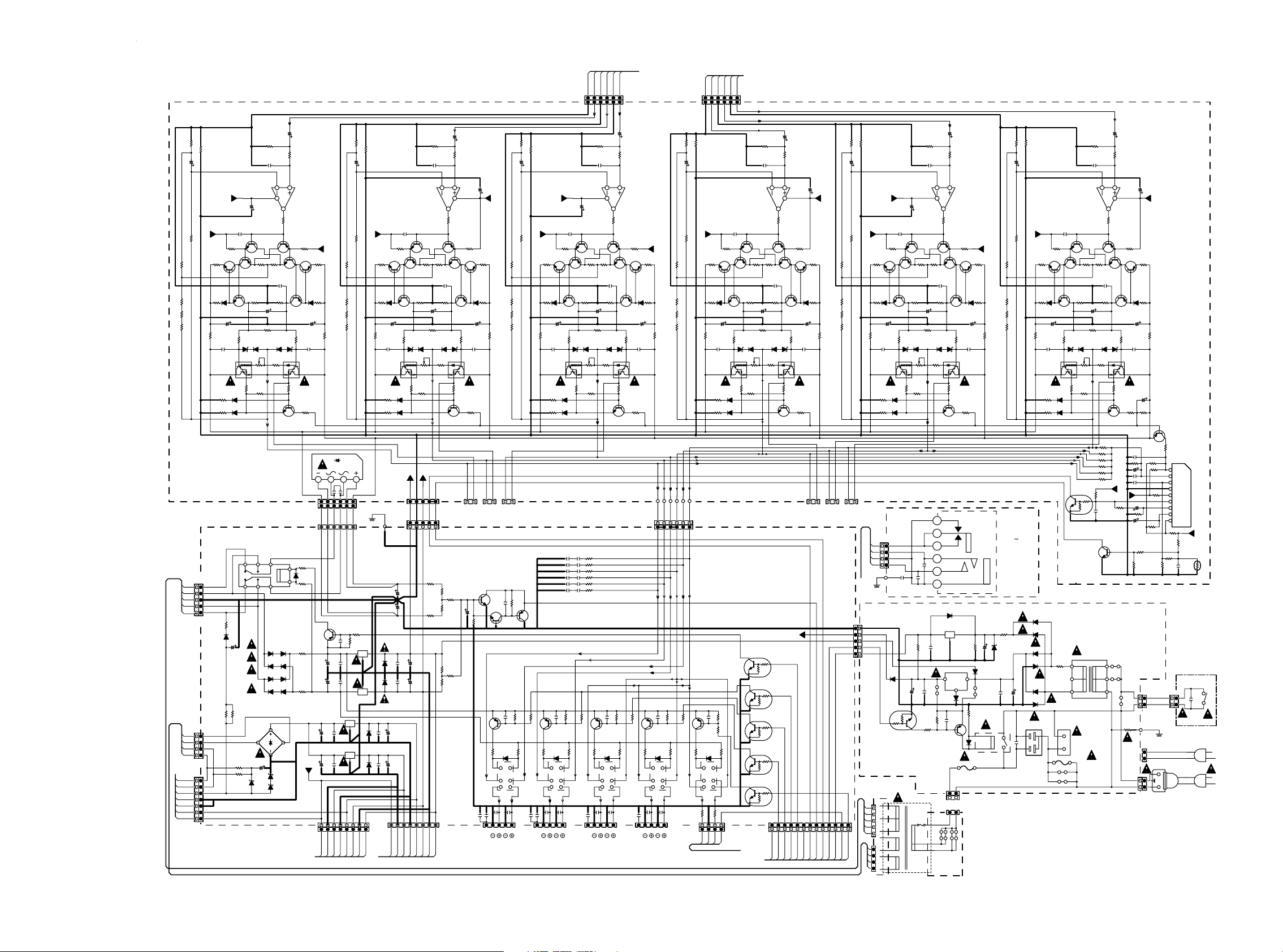
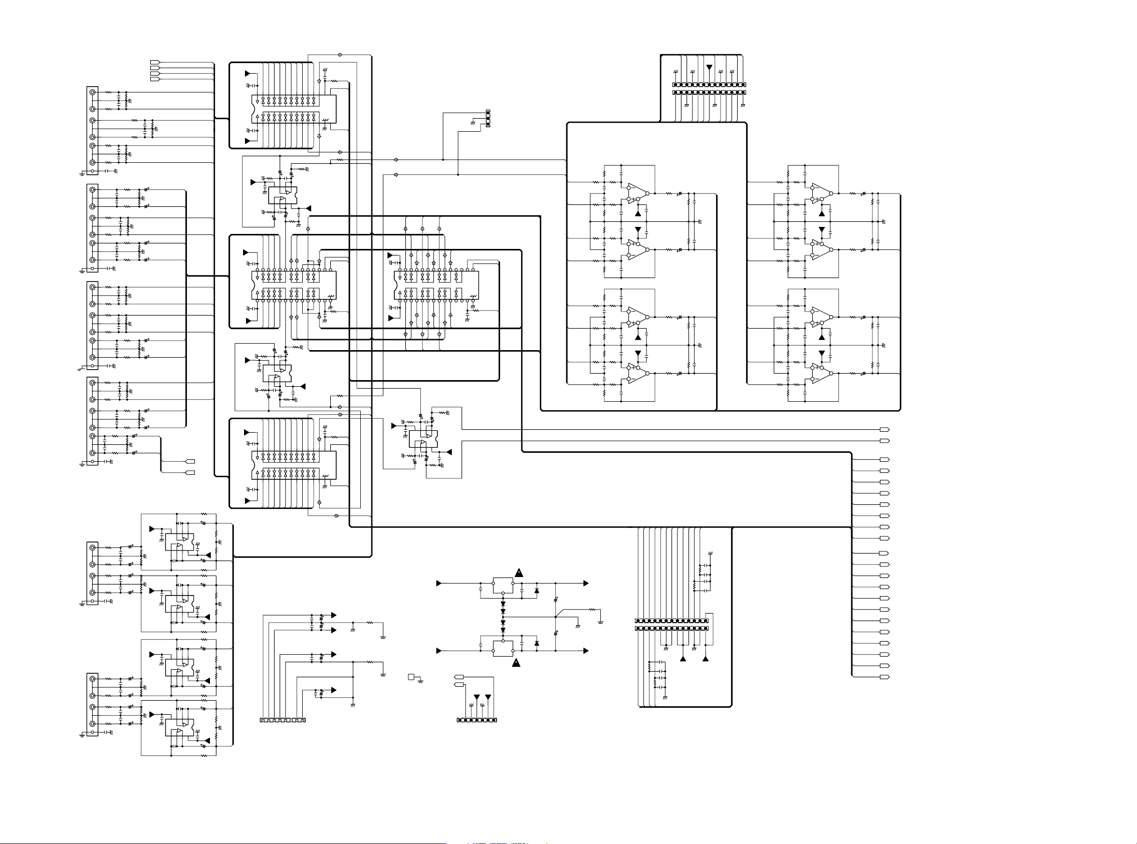
5. SCHEMATIC DIAGRAM
FROM JE09(PS04:Audio PCB)
S-GND
6
J102
6
EH
FROM JE08(PS04:Audio PCB)
FL
FR
S-GND
SL
S-GND
SR
C
SB
S-GND
S-GND
12345
12345
S-GND
12345
6
J101
PH
12345
6
R350
15
R352
10
C320
100 50V
47/16V(OSE)
-12V
R368
33k
R346
47 1W
R314
470
R344
120 1W
R322
150
R342
120 1W
R340
120 1W
220/63V(OSE PS)
220/63V(OSE PS)
R334
10 1 4w
55 0
P104
RMA (@1@@ @3@@) POWER AMPS
RMC (@N@@) PROTECTIONS
From Main Transfomer
AC41 0
1
1
AC14 9
2
2
0
3
3
AC14 9
4
4
AC41 0
5
5
J801
VH
EH
J802
From Main Transfomer
1
1
2
2
3
3
4
4
TO JC02(PC04:
Display PCB)
FL2
1
1
FL1
2
2
VKK
3
3
GND
4
4
GND
5
5
+5VD
6
6
+5VL
7
7
J803W803
PH
R302
33k
C304
330p
0
100/16V
2
3
2SA970
Q310
330k
123
R326
1 3
D308
D312
3 9V
13
4
123
R358
LN99
24316
1.5k 1W
C322
2SC2458
Q306
123
R318
68
C310
2
R338
220
680
C819
Dummy
D816
6.8V
4
R316
68
22/50V
R366
680
R336
0
LY2 0
5
D802
D804
D806 D807
D808
1
D817
D818
123
C308
2200p
R324
330k
D306
10
1A
1A1A1A
1A 1A
1A
4
30V
Jumper
-12V
C306
10p
R310
10k
0 6
Q312
2SC2240
1
53 1
D304
Q318
2SC2705
C314
100/63V
100/63V
R330
100
C318
Dummy
5
Q322
SAP17P
R360
22k
D314
HSS81
R362
22k 22k
HSS81
D316
R801
1 1/4W
1A
D810
C820
100 63V
R802
R805
2.2k 1W
AC7 9
R803
100 1/4W
21 3
21 3
R804
100 1/4W
28 8
C302
10/50V
R304
1k
0
32
Q301
2068
OP AMP1 2
1
0
R306
100
0
Q304
2SA1048
R308
+0 6
123123
1
Q314
2SC2240
123
Q316
2SA1145
220/63V(OSE PS)
+1 3
D310
3 9V
1
2
543
R354R356
1k1k
123
Q324
2SC2240
RN68
150 1 4W
7
8
150 1/4W
D803
D805
1A
D809
+17 6 +17 3
1 1 2W
R812
1 1 2W
17 6
23
D801
6GBU02
R328
100
RN69
R811
Q308
2SA970
Q320
SAP17N
R364
DN55
10k
2
100/63V
Dummy
0.1A
+8 4
+53 1
C312
C316
+5VL
+12V
R312
3
470
D302
R320
150
+55 0
C822
0 1
VH
1234 56
J805
1234 56
W805
123456
SDN
1
3
C803
2200 35V
C804
2200/35V
17 3
C815
10000 16V
C816
R332
D10XB40
QN55
2SA1048
6800/16V
10/50V
2068
Q301
33k
R301
C303
330p
R315
68
22/50V
680
R335
0
PA FAIL
15k
RN74
15k
RN75
15k
15k
1
+12V212VG3-12V4+5VD5+5VDG6+5VV75VVG8+5VL
0
6
0
123
Q313
2SC2240
C307
2200p
R323
330k
+1 3
D305
10
2
543
2SC2240
HEAT DET
RN72
22k
RN73
10k
RN78
22k
RN79
W808
SAN
D309
3 9V
7
100
R305
0
Q323
10k
R303
0
2SA1048
Q303
+0 6
123
2SA1145
Q315
R353
1k
5
C301
1k
8
R307
10k
1
123
2
Q307
2SA970
+53 1
D301
C311
100 63V
220/63V(OSE PS)
R327
100
C315
Dummy
1
Q319
SAP17N
R363
22k
123
2
SB
Idring Adjust Test Points
+5 0
+5 0
QN60
2SC2458
0
47/16V
CN56
R349
15
R351
10
C319
100/50V
47/16V(OSE)
OP AMP2/2
C305
12V
R313
470
R321
150
220/63V(OSE PS)
101 4w
R333
J804
GND
27000/65V(OSE)
13
0 1
C813
C814
PH
J809
W809
2SC2240
Q311
53 1
D303
C313
100 63V
Dummy
C317
Q321
SAP17P
55 0
R359
22k
R361
22k
C801
15000/63V
27000/65V(OSE)
15000/63V
1A1A
D811D812
0.1
TO JS05(PS04:Audio PCB)TO J980(PD04:Digital I/O PCB)
10k
R309
2SC2705
R329
100
D313
D315
SCN
W806
EH
C802
0 01
C809
0 01
C810
C817
100/10V
C818
100/10V
10p
0 6
2
123
2SA970
Q309
123
Q317
1 3
D311
3 9V
5
R355
1k
HSS8
HSS81
+12V
12345
12345
J806
12345
C805
C806
R325
330k
D307
4
123
R357
P-GND
100/16V
100/16V
2SC2458
Q305
123
R317
3
68
C309
R365
R337
2
220
13
680
-12V
RN76
RN77
33k
R367
R345
47 1W
R343
120 1W
R341
120 1W
R339
120 1W
101/4w
D821
1234
1234
C821
0 1
EARTH
+55 0
55 0
CN55
RN80
10k
1000p
2
RN55
10k
Q801
7812
2
C807
0.01
3
C808
0.01
7912
21
Q802
13
7805
1A1A
2
Q803
0.1
C811
C812
D813
Q804
13
7805
2
0.1
D814
12345678
1
+12V212VG3-12V4+5VD5+5VV6+5VV75VVG8+5VL
R250
15
10
R252
C220
100/50V
47/16V(OSE)
100/16V
C321
+12V
33k
R311
470
3
R319
150
+55 0
1
B2B-PH
2
3
RN70
33k
CN96
0.1
47 1W
R246
120 1W
R244
120 1W
R242
R240
101/4w
120 1W
R331
121
2
J106
J104
1
CN94
0.1
J108
B2B-PH
B2B-PH
C
SR
CN57
RN71
1000p
100k
2SC2458
3
1
220 1/4w
Dummy
+5 0
3
QN61
123
2
1
QN62
2SA1048
RN54
CN54
10k
1000p
RN59
2
QN54
2SA1048 2SA1048 2SA1048 2SA1048
DN54
1A
RN67
RN66
330 1/4w
32 6
45 1
LN54
0000000000
CN95
C276
C376
Dummy
43215
J174 J173 J172
SB
SL
R268
0
12V
R214
470
150
R222
220/63V(OSE PS)
101/4w
R234
55 0
3
10k
1
220 1/4w
0.1
CN93
Dummy
SR
C214
Dummy
C218
R260
R262
RN65
2SC2240
Q212
53 1
D204
100 63V
SAP17P
22k
22k
2
QN53
1A
DN53
45 1
LN53
C275
100
R230
Q222
HSS81
HSS81
C273
C274
C373
C374
CN53
1000p
CENTER
12V
10k
R210
D214
D216
C206
10p
0 6
2SC2705
Q218
R256
0 022
0 022
0 022
0 022
0 022
RN53
10k
RN64
32 6
C375
43215
123
1k
Dummy
2SA970
Q210
3 9V
D212
5
330 1/4w
C222
100/16V
2SC2458
2
R218
3
330k
123
R226
C210
1 3
D208
R238
220
4
13
123
R258
C172C174
C271
C272
C371
C372
10k
RN58
0.1
CN92
SPEAKER OUTPUTS
10/50V
C202
33k 33k
R202
1k
R204
C204
330p
00
3
2
2068
Q201
4
OP AMP1/2
1
0
100
R206
0
2SA1048
Q204
R208
+0 6
123
10k
+12V
2SA970
Q208
R212
1
3
123
470
2SC2240
Q214
2
+53 1
D202
150
123
R220
2SA1145
Q216
C212
100/63V
220/63V(OSE PS)
101/4w
100 100
R232
R228 R227
3 9V 3 9V
Dummy
D210 D209
C216
1
SAP17N SAP17N
Q220 Q219
+55 0
1k
R254
22k
R264
123
Q224
W179-6
W179
6
6
10k
RN52
3
CN51
RN57
RN62
330 1/4w
32 6
C177
0.1
Dummy
43215
10k
10k
1000p
2
QN51
1
1A
DN51
RN61
220 1/4w
32 6
45 1
LN51
C176
Dummy
CN91
FL(A) FR(A)
0
RN63
R216
22/50V
10 1w
10 1w0 022
10 1w
10 1w
10 1w
10 1w
68
R224
R236
10
2
QN52
1A
DN52
45 1
LN52
C178
2200p
C208
330k
D206
CN52
FR(B)
+1 3
1000p
2
543
2SC2240
68
680
R171
R172C171C173
R271
R272
R371
R372
Q206
123
2
FL(B)
3
1
220 1/4w
Dummy
C175
J171
W179-5
RN60
43215
R249
W179-4
SRSBCFRSL
RN51
330 1/4w
Dummy
10
R251
15
C219
100/50V
47/16V(OSE)
12V
33k
R267
2SC2240
R213
47 1W
R245
470
53 1
150
120 1W
R243
R221
120 1W
120 1W
W179-3
D203
R241
C213
100/63V
R239
220/63V(OSE PS)
101/4w
R233
Dummy
C217
55 0
R259
22k
R261
22k
W179-1
W179-2
12345
J179
12345
VH
P804
RMB (@1@@ @3@@) POWER AMPS
RPS (@8@@) POWER SUPPLY
FL
000000
3
CP91
RN56
10k
1000p
2
QP92
1
2SA1048
RP96
1A
DP91
RP94
220 1/4w
45 6
32 1
LP91
RP91
330 1w
330 1w
4
4
Q211
SAP17P
10k
C205
10p
10k
R209
0 6
123
2SA970
Q209
2SC2705
Q217
1 3
100
R229
3 9V
D211
5
Q221
1k
R255
HSS81
D213
HSS81
D215
RP95
10k
RP93
330 1/4w
+5 0
RP92
JP91
123
EH
WP91
123
TO JP92(PP94:Head Phones PCB)
R201
C203
330p
2068
Q201
OP AMP2 2
2SC2458
Q205
123
2
R215
R217
3
68
68
2200p
C207
330k
330k
123
R225
R223
22/50V
C209
D207
D205
R237
R235
10
2
220
4
13
123
0
680
R257
QN59
1
DTC114
2
3
QN58
1
DTC114
3
QN57
1
DTC114
3
QN56
DTC114
1
3
QP91
1
DTC114
3
J810
FFC
WC02
NC
TO JU04(P604:u Com DSP PCB)
10/50V
C201
1k
R203
00
5
6
8
7
0
100
R205
0
2SA1048
Q203
R207
+0 6
123
10k
2SA970
Q207
1
123
2SC2240
Q213
2
+53 1
D201
123
2SA1145
Q215
C211
100/63V
220/63V(OSE PS)
+1 3
Dummy
C215
1
2
543
+55 0
1k
R253
22k
R263
123
2SC2240
Q223
Idring Adjust Test Points
+5VL
0
2
2
2
2
12345
678
12345
678
NC
HEAT
SURR ON
FLRB ON
FLRA_ON
100/16V
C221
+12V
R211
3
470
150
R219
101/4w
R231
12121
J103
B2B-PH
FR
101112
9
9
101112
PL FAIL
HEAT DET
_PA_FAIL
_STANDBY
R150
15
B2B-PH
SL
GND
+5VL
PR POWER
STANDBY
P DOWN
P DOWN
_HP_DET
10
R152
C120
100/50V
47/16V(OSE)
12V
33k
R168
R114
47 1W
R146
470
150
120 1W
R144
R122
120 1W
R142
100/63V
R140
220 63V(OSE PS
101/4w
120 1W
R134
Dummy
C118
55 0
R160
R162
2
J105
J107
B2B-PH
FL
WP91
1
2
3
4
EARTH
TO JP91(P804:Power Supply PCB)
5
5
4
4
3
+12 0
3
2
+5 0
2
1
+5 0
1
J807
J853
JQ
XH S
P894
SDN
W891
1
2
3
13
4
5
13
1
HP_ON
2
3
4
SCN
W892
2SC2240
53 1
D104
C114
22k
22k
WP93
DTC114
9
8
7
6
5
4
3
Q112
SAP17P
Q853
Q122
Jumper
R110
D858
B
2
10k
100
R130
HSS81
D114
HSS81
D116
JP92
EH
1
2
3
4
1A
12V
2SC2705
HP DET
HP R
GND
HP L
C106
10p
123
123
2SA970
Q110
123
Q118
1 3
3 9V
D112
5
1k
R156
CP92
0 1
E
C
T001
MAIN TRANSF
330k
R126
100/16V
C122
100 16V
2SC2458
C110
D108
220
4
13
123
680
R158
Dummy
R853
C855
3
1
R138
33k
R102
C104
330p
2
4
0
Q106
123
123
R116R118
6868
2200p
C108
330k
R124
22/50V
+1 3
D106
R136
2
10
2
543
0
0
2SC2240
JP99
CP94
Dummy
CP93
D862
S 80842CNY
RESET IC (4 2V)
+5 0
OUT
3
0.1
C856
47k
31
2
B852
0 1
Dummy
C854
1
4.7k
R855
R854
10k
VA
J854
W861
1
2
2
B853
1
100
R106
0
2SC2240
Q114
3 9V
D110
Q124
9
8
7
3
2
1
Q852
2
78M05
1000p
Q854
2SA1048
SDN
B854
220V(K)
2SA1048
2SA1145
D861
1
1
1
10/50V
C102
1k
R104
00
3
2068
Q101
OP AMP1/2
Q104
R108
+0 6
10k
2SA970
Q108
1
123
123
Q116
220/63V(OSE PS)
100
R128
1
SAP17N
Q120
1k
R154
0
22k
R164
123
HEAD PHONES OUT
0 1A
VDD
1
VSS
Q851
INOUT
GND
2
0.1A
Jumper
C858
3
E
2
B
1
C
F851
1
J856
AC250V 10A (U F)
AC250V T5AL (N K)
2
2
2
1121
B854
B853
100V(F)
120V(U)
230V(N)
+12V
R112
3
470
2
+53 1
D102
150
R120
C112
100 63V
Dummy
C116
+55 0
15k
R852
2
B851
1
1 1/4w
R856
1A
D860
41
1
J857
P864
R132
4 7/50V
C857
D857
Jumper
L851
TV 8
101/4w
1A
Dummy
R149
15
C119
47 1W
120 1W
120 1W
120 1W
PP94
(RHP)
XP91
2 2k 1/6w
R851
D859
8.2V
+10 4
0 1
C852
C853
3300 25V
23
C851
R145
R143
R141
R139
100/50V
47/16V(OSE)
33k
R167
1A
1A
AC OUTLETS
34
0 01
10
R151
12V
R113
470
150
R121
220/63V(OSE PS)
101/4w
R133
1A
D851
D852
1A
D853
1A
D854
1A
D855
D856
J860
(U F)
OP AMP2/2
C105
10p
10k
2SC2458
R109
2SC2240
Q111
R117
123
123
2SA970
Q109
330k
123
R125
D103
2SC2705
Q117
C109
100
R129
D107
3 9V
D111
R137
5
SAP17P
220
4
Q121
13
123
1k
R155
680
HSS81
R157
D113
HSS81
D115
+5 0
QN04
DTC114
1
3
P854
RPS (@8@@) POWER SUPPLY
RBU (@8@@) BUCK UP POWER SUPPLY
Backup Trans
R857
9
Jumper
13 3
AC OUTLET
J806(N)
2
1
J858J859
(N)(N)
1
1
AC250V T2 5AL
B854
(U F)
1
2
B853
(U F)
1
2
100/63V
Dummy
C117
R159
22k
R161
22k
C113
1
10 50V
C101
33k
R101
1k
R103
C103
330p
00
56
0
RN02
RN03
RN04
RN05
RN06
R115
22/50V
RN01
(N)
68
C107
R123
R135
10
22k
RN17
4700p
CN09
1
3
0
123
3
2SC2240
2200p
330k
+1 31 3
D105
2
543
R153
1k
2SC2240
68k
68k
68k
68k
68k
68k
C
QN03
E
T851
4
15
7
100
R105
0
Q113
123
D109
3 9V
Q123
CN03
0 01
RN07
33k
CN04
47/50V
CN02
0 01
+12V
2
B
2SC2458
2
B856
2
B857
8
Q103
2SA1048
+0 60 60 6
2
Q115
2SA1145
RN12
1k
C121
100/16V
10k
R107
Q107
2SA970
1
1
2
+53 153 1
D101
C111
100 63V
220/63V(OSE PS)
R127
100
Dummy
C115
1
Q119
SAP17N
R163
22k
123
CN08
0 01
0 47/50V
CN06
Dummy
1
100V,120V,230V
(F)
220V
(K)
(U)
2
B855
1
R860
(U)
2 2M
VA
J851
3
R111
470
R119
150
+55 055 0
0
12V
RN22
10k
10k
RN23
(U) (N)
1
2
VA
J852
J861
1
2
RN08
GND
R131
CN05
RN13
33k
RN14
1
2
1
2
1
2
W871
VA
+12V
10 1/4w
CN01
4 7/50V
RN16
6 8k
100k
RN10
100k
RN11
3 3k
1k
RN21
(N K F)
W852
EARTH
AC INLET(N K F)
QN02
2SA970
123
RN09
22k
0
1
2
3
4
5
6
7
8
9
QN01
TA7317P
RN15
+12V
3 3k
RN18
15k
Heat Sens Temp
100C’
RN20
10k
CN07
4.7k
0.01
RN99
For HEAT Sens
P884
N K F)
VA
J881
1
1
2
S881
C881
0.027
2
21
(RSW)
AC CORD(U)
W001
L
1
2
N
J871
AC CORD(N,K,F)
Z011
2068
Q101
Q105
123
68
680680680680
R165R166R265R266
2
2
+5 0
F852
9 10
Page 10
TV
DVD
VCR1 IN
VCR1 OUT
DSS/VCR2 IN
DSS/VCR2 OUT
CD
TAPE IN
TAPE OUT
CDR/MD IN
CDR/MD OUT
MULTI
FRONT
(AUX2)
SURROUND
7.1CH INPUT
SURROUND
BACK
CENTER
SUB WOOFER
A GND
JUMPER
CE TCA
AFDATA
AFCLK
JUMPER
AFDATA
AFCLK
CE TCB
RS62
100
RQ35
CE TCA
AFDATA
AFCLK
M FR
M FR
ANA FR
ANA FL
M FL
M FL
RQ72
+12V-12V
JUMPER
GND
EARTH
JUMPER
RQ71
EARTH
+5VL +5VD
D GND
PS04-1/2
RRJ(XSXX) AUDIO FUNCTION
RCR(XQXX) 7 1CH IN FUNCTION
RRM(XMXX) MULTI FUNCTION
RDD(XHXX),(XJXX) DAC LPF
TO A D Rch
TO A D Lch
D-SR
+12V
28 27 26 25 24 23 22 21 20 19 18 17 16 15
A-GNDA-GND
VD D
VEE
1234567891011121314
CS81
0 1
-12V
D-SL
CM02
10 50V
RM02
100k
A-GND
-7V
CM07
0 1
A GND
RM01
100k
A-GND
CM01
10/50V
JS99
GND TERMINAL
D-SW
D-SBR
M-SR
M-SL
SR-V
SL-V
EARTH
M SW
M-SBR
SBR-V
SBL-V
M-SBL
M-CNT
D-SBL
D-CNT
RM04
Dummy
CM04
100k
CM06
10 50V
123+4
QM01
NJM4558DD
8765
CM08
CM05
0 1
10/50V
Dummy
CM03
RM03
A-GND
100k
-12V +12V
AUX R
AUX L
JS06
07 FMN BTK A
SW-V
CNT-V
A-GND
JS51
B3B PH
Dummy
1
2
3
A GND
RT
LT
FL
FL+
FR+
AFDATA
AFCLK
F_CLK
F_DATA
QS04
TC9162AN
F_ST
A GND
CE TCB
RS64CS82
100100p
A GND
+7V
NJM78M06FA
QQ61
31
CQ83
0 01
CQ84
0 01
D GND
NC
AUX-L
D-GND
5
6
7
OUTIN
GND
CQ87
0 1
2
DQ81
0 1A
DQ83
0 1A
DQ84
0 1A
DQ82
0 1A
1
CQ88
0 1
GND
OUTN
32
NJM79M06FA
QQ62
+12V12V
A GND
-12V
+12V
AUX-R
A-GND
1
2
3
4
FR
SL
SL+
SR+
SR
A GND
RQ73
JUMPER
+7V
-7V
DQ85
1A
CQ89
100/16V
CQ90
100/16V
DQ86
1A
CH09
RH09
470p
8 2k
RH01
3 9k
CH01
3300p
CH05
3300p
RH05
3 9k
RH06
3 9k
CH06
3300p
CH02
3300p
RH02 RJ02
3 9k 3 9k
RH03
3 9k
CH03
3300p
CH07
3300p
RH07
3 9k
RH08
3 9k
CH08
3300p
CH04
3300p
RH04
3 9k
EARTH
QH01
NJM2068DD
2
RH17
1 8k
RH21
1 8k
RH13
8 2k
RH14
8 2k
RH22
1 8k
RH18
1 8k
RH10
8 2k
RH11
8 2k
RH19
1 8k
RH23
1 8k
RH15
8 2k
RH16
8 2k
RH24
1 8k
RH20
1 8k
RH12
8 2k
CH13
470p
CH14
470p
CH10
470p
CH11
470p
CH15
470p
CH16
470p
CH12
470p
3
5
6
2
3
5
6
OP AMP1/2
7V
+7V
OP AMP1/2
7V
+7V
OP AMP2/2
QH02
NJM2068DD
JS11JS11
4
8
QH01
QH02
NJM2068DD
4
8
L/RMUTE
SLSRMUTE
14 L/RMUTE
15 SLSRMUTE
1CE VOLB
2_CE_VOLA
CE VOLB
_CE_VOLA
1
7
1
7
100
RS65
CH49
0 1
CH51
0 1
CH50
0 1
CH52
0 1
SBMUTE
16 SBMUTE
3VOLCLK
VOLCLK
TO AUX PCB
AUX L
AUX R
TUNER L
JS01
RS01
7
L
9
8
R
RS02
4
L
6
5
R
RS09
1
L
3
2
R
RS10
10
CS47
JUMPER
JS02
7
L
9
8
R
RS17
4
L
6
5
R
RS18
1
L
3
2
R
10
CS48
JUMPER
JS03
RS25
7
L
9
8
R
RS26
RS29
4
L
6
5
R
RS30
1
L
3
2
R
10
CS49
JUMPER
JS04
RS37
7
L
9
8
R
RS38
4
L
6
5
R
1
CS43
L
470p
3
CS44
470p
2
R
10
CS50
JUMPER
JQ01
RQ01
4
L
6
5
R
RQ02
RQ09
1
L
3
2
R
RQ10
7
CQ41
0 1
JQ02
RQ17
4
L
6
5
R
RQ18
RQ25
1
3
2
RQ26
7
CQ42
0 1
TUNER R
100
82k
RS03
CS01
470p
CS02
470p
82k
100
RS04
100 82k
RS05 RS07
CS03
470p
CS04
A-GND
470p
100 82k
RS06 RS08
100
82k
RS11
CS05
470p
CS06
A-GND A-GND
470p
82k
100
RS12
A GND
1k
RS13
CS07
RS15
470p
47k
RS16
CS08
47k
470p
1k
RS14
82k
100
RS19
CS11
470p
CS12
A-GND
470p
82k
RS20
100
1k
RS21
CS13
RS23
470p
47k
RS24CS14
47k470p
1k
RS22
A-GND
82k
100
RS27
CS17
470p
CS18
A-GND
470p
82k
100
RS28
100
82k
RS31
CS19
470p
CS20
A-GND
470p
82k
100
RS32
1k
RS33
CS21
RS35
470p
47k
RS36CS22
47k470p
1k
RS34
A-GND
100
82k
RS39
CS25
470p
CS26
470p
82k
100
RS40
1k
RS41
RS43
CS39
47k
470p
CS40
RS44
470p
47k
1k
RS42
100
RS45
CS45
RS47
JUMPER
47k
RS48
A-GND A-GND
47k
CS46
100
RS46
JUMPER
A GND
CQ03
100
10/50V
CQ01
RQ03
470p
47k
CQ02
RQ04
470p
47k
CQ04
100
10/50V
CQ11
10/50V
100
RQ11
CQ09
47k
470p
CQ10
RQ12
470p
47k
CQ12
100
10/50V
A-GND
100
CQ19
10/50V
RQ19
CQ17
47k
470p
CQ18
RQ20
47k
470p
10/50V
100
CQ20
100
10/50V
CQ27
CQ25
RQ27
470p
47k
CQ26
RQ28
470p
47k
10/50V
100
CQ28
A-GND
A-GND
A-GND
CS23
10/50V
CS24
A-GNDA-GND
10/50V
CS41
10/50V
CS42
10/50V
MULTI L
MULTI R
-12V
A-GNDA-GND
-12V
A-GNDA-GND
CS09
10/50V
CS10
10/50V
CS15
10/50V
CS16
10/50V
-12V
VC1OUT L
VC1OUT R
DSSOUT L
DSSOUT R
TAPOUT L
TAPOUT R
CDROUT L
CDROUT R
MULTI L
MULTI R
CQ51
0 1
NJM4558DD
A GND
QQ01
CQ06
Dummy
CQ53
0 1
NJM4558DD
A GND
+
QQ02
CQ14
Dummy
CQ55
0 1
A GND
NJM4558DD
QQ03
CQ22
Dummy
-12V
CQ57
0 1
A GND
NJM4558DD
QQ04
CQ30
Dummy
AUX L
AUX R
TUNER L
TUNER R
TV L
QS02
TC9273N 013
MULTI
TV R
DVD L
DVD R
VCR1 N L
VCR1 N R
DSSIN L
DSSIN R
CD L
CD R
TAPE N L
TAPE N R
CDRIN L
CDRIN R
MULTI L
MULTI R
Dummy
RQ05
CQ05
Dummy
10/50V
CQ07
1234
+
A GND
CQ52
0 1
8765
10/50V
CQ08
Dummy
RQ06
Dummy
RQ13
CQ13
Dummy
10/50V
CQ15
1234
+
A GND
CQ54
0 1
8765
10/50V
CQ16
Dummy
RQ14
Dummy
RQ21
CQ21
Dummy
10/50V
CQ23
1234
+
A GND
CQ56
0 1
8765
10/50V
CQ24
Dummy
RQ22
CQ29
Dummy
RQ29
Dummy
10/50V
CQ31
1234
+
A GND
CQ58
8765
0 1
10/50V
CQ32
Dummy
RQ30
Rch
MAIN
+12V
QS03
TC9164AN
+12V
QS01
TC9273N 013
MULTI
Lch
MAIN
M FL
RQ07
47k
A-GNDA-GNDA-GNDA-GND
RQ08
47k
+12V
M FR
M SL
RQ15
47k
RQ16
47k
+12V+12V
M SR
M SBL
RQ23
47k
RQ24
47k
M SBR
M CNT
RQ31
47k
RQ32
47k
+12V
M SW
CD-R
DVD-R
DSSINR
CDR N-R
TAPE N-R
CS77
0 1
A GND
28 27 26 25 24 23 22 21 20 19 18 17 16 15
1234567891011121314
A-GND
CS78
0 1
-12V
-12V
CS74 CS80
0 1 0 1
28 27 26 25 24 23 22 21 20 19 18 17 16 15
A-GNDA-GND
VCR1 N-R
VDD
VSS
CDRIN R
TAPEIN-R
CD-R
DSSIN-R
VCR1IN-R
DVD-R
CS58
10/50V
RS56
Dummy
CS60
220k
A-GNDA-GND
CS64
0 1
NJM4558DD
A GND
+
RS52
220k
CS56
CS52
10/50V
10/50V
CS54
Dummy
RS54
47k
ANA-FR
DSSOUT-R
VC1OUT-R
TAPOUT-R
CDROUT R
VDD
VEE
1234567891011121314
CS75
0 1
-12V
VC1OUT-L
DSSOUT-L
TAPOUT-L
CDROUT-L
ANA-FL
CS51
10/50V
RS53
RS51
Dummy
CS53
47k
220k
NJM4558DD
+
RS55
220k
CDRIN-L
TAPEIN-L
CDR N-L
TAPEIN-L
+12V
1
2
FROM P804
+12VG
CS55
10/50V
123+4
8765
CS61
10/50V
Dummy
CS59
47k
RS57
CD-L
DVD-L
DSS N-L
VCR1IN-L
CD L
DSSIN-L
VCR1IN-L
DVD-L
-12V
+5VD
+5VDG
3
4
5
6NC7
A-GND
-12V
CS63
0 1
A GND
A-GND
CS57
10/50V
CS71
0 1
A-GNDA-GND
28 27 26 25 24 23 22 21 20 19 18 17 16 15
VDD
VSS
1234567891011121314
CS72
0 1
-12V +12V
JS05
B8B PH
A GND
TV-R
AUX-R
CS79
TUNER-R
MULTI-R
100p
RS63
100
STB
DATA
CK
A GND
MA N-R
AUX-R
TV-R
TUNER-R
RQ36
RS58
A-GND
47k
CS62
10/50V
123+4
QS06
8765
+12V
CS66
0 1
D-FR
A GND
M-FR
FR-VFL-V
F_CLK
F_DATA
F_ST
CS76
100p
A GND
M-FL
D-FL
A-GND
QS05
+12V
CS65
0 1
A-GND
A GND
TV-L
AUX LAUX-L
CS73
MULTI-L
TUNER-L
100p
RS61
100
STB
DATA
CK
A GND
MAIN-L
TV-L
TUNER-L
CQ71
CQ73
0 1
100/16V
CQ72
CQ74
0 1
100/16V
CQ75
CQ76
100/16V
0 1
CQ78
CQ77
0 1
100/16V
+5VL
+5VVG
8
FR-
1415161718
JS13JS13
123456789
A GND A GND A GND
SL-
SL+
RH25
CH17
100
22 50V
RH29
100k
RH30
100k
RH26
CH18
100
22/50V
CH19
RH27
22 50V
100
RH31
100k
RH32
100k
RH28
CH20
100
22/50V
CE TCB
P DOWN
ERMUTE
SWMUTE
CNTMUTE
MULTMUTE
P DOWN
22 CE TCB
20 ERMUTE
21
17 CNTMUTE
18 SWMUTE
19 MULTMUTE
4VOLDATA
5GND
6GND
7GND
8
9+5VD
+5VD
D GND D GND
CS83
+5VD +5VL
100p
CS84
100p
CS85
100
100p
CS86
RS66
100p
D GND
VOLDATA
FR+
_CE_TCA
23 _CE_TCA
10+5VD
SR+
AFCLK
100
RS68
24 AFCLK
11GND
CH21
1000p
CH22
1000p
CH23
1000p
CH24
1000p
FL+
SR-
100
RS67
AFDATA
25 AFDATA
12GND
FL-
19
SBL-
A-GNDA GND
26 +5VL
13+5VL
12V
202122
SBL+
D FL
D FR
D SL
D SR
D GND
CS87
100p
CS88
100p
CS89
100p
CS90
100p
LT
RT
SW-
SW+
A GNDA GNDA GNDA GND
232425
26
101112
13
SBR+
SBR-
CNT-
CNT+
CJ09
RJ09
8 2k
RJ01
3 9k
SBL
3300p
CJ05
3300p
SBL+
RJ05
3 9k
RJ06
3 9k
SBR+
3300p
CJ02
3300p
SBR
RJ03
3 9k
CNT
3300p
CJ07
3300p
CNT+
RJ07
3 9k
RJ08
3 9k
SW+
3300p
CJ04
3300p
SW
RJ04
3 9k
470p
QJ01
2
NJM2068DD
RJ17
CJ01
1 8k
OP AMP1/2
RJ21
1 8k
3
CJ13
RJ13
470p
8 2k
CJ14
RJ14
470p
8 2k
5
RJ22
CJ06
1 8k
OP AMP2/2OP AMP2/2
RJ18
1 8k
6
RJ10
CJ10
470p
8 2k
CJ11
RJ11
470p
8 2k
2
RJ19
CJ03
1 8k
OP AMP1/2
RJ23
1 8k
3
CJ15
RJ15
470p
8 2k
RJ16
CJ16
8 2k
470p
5
RJ24
CJ08
1 8k
OP AMP2/2
RJ20
1 8k
6
CJ12
RJ12
470p
8 2k
4
7V
+7V
8
QJ01
NJM2068DDNJM2068DD
QJ02
NJM2068DD
4
7V
+7V
8
QJ02
NJM2068DD
RJ25
CJ17
1
100
22/50V
CJ41
01
CJ43
01
RJ26
7
100
RJ 7
CJ19
1
100
22/50V
CJ42
01
CJ44
01
RJ28
7
100
22/50V
SW V
CNT V
FR V
FL V
SR V
SL V
SBR V
SBL V
VOLDATA
VOLCLK
CE VOLA
CE VOLB
L/RMUTE
CNTMUTE
SWMUTE
SLSRMUTE
SBMUTE
MULTMUTE
ERMUTE
P DOWN
RJ29
100k
RJ30
100k
CJ18
22/50V
RJ31
100k
RJ32
100k
CJ20
D SBL
CJ21
1000p
A-GNDA GND
CJ22
1000p
D SBR
D CNT
CJ23
1000p
CJ24
1000p
D SW
MR V
ML V
SW V
CNT V
FR V
FL V
SR V
SL V
SBRV
SBL V
VOLDATA
VOLCLK
CE VOLA
CE VOLB
L/RMUTE
CNTMUTE
SWMUTE
SLSRMUTE
SBMUTE
MULTMUTE
ERMUTE
P DOWN
1211
Page 11
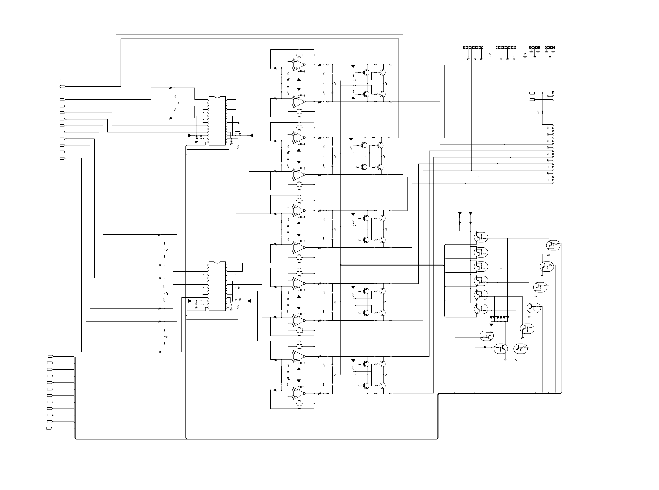
VOLDATA
VOLCLK
CE VOLA
CE VOLB
L/RMUTE
CNTMUTE
SWMUTE
SLSRMUTE
SBMUTE
MULTMUTE
ERMUTE
P DOWN
PS04-2/2
RVR(XEXX),(XGXX) 7 1CH VOLUME
RRM(XMXX) MULTI FUNCTION
MULTI L
MULTI R
SW V
CNT V
MR V
ML V
FR V
FL V
SR V
SL V
SBR V
SBL V
VOLDATA
VOLCLK
CE VOLA
CE VOLB
L/RMUTE
CNTMUTE
SWMUTE
SLSRMUTE
SBMUTE
MULTMUTE
ERMUTE
P DOWN
MR
ML
FR
FL
SR
SL
SBR
SBL
SW
CNT
22/50V
22/50V
22/50V
22/50V
22/50V
22/50V
TO POWER PCB
TO J101(P104)
MUT FLFR
MUT CNT
MUT SW
MUT SLSR
MUT SB
MUT MULT
JE08
123456
B6B EH
A GND A GND A GND A GND A GND A GND
MA N SL
MA N FL
+5VL
+12V
DM28
DM29
Jumper
Dummy
1
2
1
2
1
2
1
2
1
2
1
2
QM33
DTA144ES/UN4113
P DOWN
ERMUTE
RG68
Dummy
100p
CG66
33k
RG70
2
QG53
RM34
RM33
RG16
RG66
47 25V
10 50V
RG65
CM34
10 50V
RE16
CE14
10 50V
RE15
RE66
CE64
10 50V
CE63
10 50V
RE65
CG14
10 50V
CG13
10 50V
RG15
4 7k
CG64
CG63
5
6
4 7k
CM33
10 50V
5
6
CE13
10 50V
5
6
8 2k
5
6
8 2k
8 2k
5
6
NJM2068DD
1
CG70
4
CG68
0 1u
CG67
0 1u
8
NJM2068DD
RG69
100p
Dummy
100p
QM13
NJM2068DD
4
CM38
0 1u
CM37
0 1u
8
RM37
100p
Dummy
100p
QE03
4
CE18
0 1u
CE17
0 1u
8
QE03
NJM2068DD
RE19
100p
Dummy
100p
NJM2068DD
4
CE68
0 1u
CE67
0 1u
8
QE53
NJM2068DD
100p
Dummy
100p
RG20
QG03
4
CG18
0 1u
CG17
0 1u
8
NJM2068DD
15k
100p
Dummy
A-GNDA-GND
A-GND
7
QG53
RM38
1
A-GND
7
QM13
NJM2068DD
RE20
NJM2068DD
1
A-GNDA-GND
7
RE70
1
A GNDA-GND
7
RE69
NJM2068DD
1
A-GND A-GND
7
QG03
47/25V
RG72
47k
RG71
47k
CG69
47/25V
4 7k
4 7k
CM40
47/25V
RM40
RM39
CM39
47/25V
4 7k
4 7k
CE20
47/25V
CE19
47/25V
4 7k
15k
CE70
47/25V
CE69
47/25V
15k
15k
CG20
47/25V
RG22
RG21
CG19
47/25V
3
12V
+12V
4 7k
CG65
RG67
RM36
D mmy
CM36
2
3
12V
+12V
4 7k
CM35
RM35
RE18
Dummy
CE16
2
3
4 7k
12V
+12V
4 7k
CE15
RE17
RE68
Dummy
CE66
2
QE53
3
12V
+12V
8 2k
CE65
RE67
RG18
Dummy
CG16
2
3
12V
+12V
RG19
CG15
RG17
CG62
22/50V
OP AMP1/2
RG62
47k
CG60
22/50V
QE12
A GND
A GND
TC9499N
1
2
A GND A1
3
4
5
6
7
8
A GND B1
9
10
11
12
13
CE82
14
0 1u
QE11
TC9499N
1
2
A GND A1
3
4
5
6
7
8
A GND B1
9
10
11
12
13
CE86
14
0 1u
IN A1
IN A2
A GND A2
IN B1
NC
IN B2
IN C1
A GND C2
IN C2
VSS
GND
CK
IN A1
IN A2
A GND A2
IN B1
NC
IN B2
IN C1
A GND C2
IN C2
VSS
GND
CK
OUT A1
A GND A2
OUT A1
OUT B1
OUT B2
A GND C1
OUT C1
OUT C2
OUT A1
A GND A2
OUT A1
OUT B1
OUT B2
A GND C1
OUT C1
OUT C2
28
27
26
25
NC
24
23
NC
22
21
20
A-GND
19
TEST
CE84
0 1u
18
CE83
17
VDD
16
STB
15
DATA
A GND
28
27
26
25
NC
24
23
NC
22
21
20
19
TEST
18
17
VDD
16
STB
15
DATA
A GND
+7V
47/25V
CE41
100p
RE45
100
A-GND
CE88
0 1u
CE87
47/25V
+7V
RE44
CE42
100100p
RG60
47k
A-GND
RG59
47k
CG59
22/50V
7V
CE81
47 25V
VOLCLK
VOLDATA
CE VOLB
CE10
RE10
47k
A-GNDA-GNDA-GND
RE09
47k
CE09
CE60
RE60
47k
RE59
47k
CE59
CG10
RG10
47k
RG09
47k
CG09
-7V
CE85
VOLCLK
VOLDATA
CE VOLA
47/25V
RG61
47k
CG61
22 50V
OP AMP2/2
CM32
22 50V
OP AMP1/2
RM32
47k
RM31
47k
CM31
22 50V
OP AMP2/2
CE12
22 50V
OP AMP1/2
RE12
47k
RE11
47k
CE11
22 50V
OP AMP2/2
CE62
22 50V
OP AMP1/2
47k
RE62
RE61
47k
CE61
22 50V
OP AMP2/2
CG12
22 50V
OP AMP1/2
RG12
47k
RG11
47k
CG11
22 50V
OP AMP2/2
SW
RG74
220
RG73
220
12V
CG72
RG84
470p
1M
MUT SW
MUT CNT
A-GND
RG83
1M
CG71
470p
12V
CNT
MR
RM42
220
47k
47k
RM41
220
12V
MUT MULT
RM48
RM51
1M
RM47
CM42
470p
A-GND
CM41
470p
ML
FR
RE24
220
RE22
CE22
47k
CE21
RE21
47k
470p
RE23
220
12V
470p
RE33
1M
MUT FLFR
A-GND
FL
SR
RE74
220
RE72
CE72
47k
CE71
RE71
47k
RE73
220
12V
470p
RE83
1M
MUT SLSR
A-GND
470p
SL
SBR
RG24
220
CG22
47k
470p
CG21
47k
RG23
220
12V
RG33
1M
MUT SB
A-GND
470p
SBL
10k
QM16
10k
RG80
10k
QG56
QG55
2SC2878
RG79
10k
3
2SC2878
QM15
2SC2878
RE30
10k
QE06
QE05
2SC2878
RE29
10k
RE80
10k
QE56
QE55
2SC2878
RE79
10k
RG30
10k
QG06
QG05
2SC2878
RG29
10k
2SC2878
3
2SC2878
2SC2878
2SC2878
RG76
RG78
220
1
3
2
2
3
1
RM44
1
RM50
2
2
RM49
1
RM43
1
3
2
2
3
1
1
3
2
2
3
1
1
3
2
2
3
1
33
1
3
QG58
2SC2878
RG82
2
10k
A-GND
2
3
QG57
2SC2878
RG81
1
10k
RG75
RG77
220
33
RM46
33
220
1
3
QM18
2SC2878
2
10k
A-GND
2
3
QM17
2SC2878
10k
1
RM45
33
220
RE26
RE28
220
33
1
3
QE08
2SC2878
RE32
2
10k
A-GND
2
3
QE07
2SC2878
RE31
10k
1
RE25
RE27
220
33
33
RE76
RE78
220
1
3
QE58
2SC2878
RE82
10k
2
A-GND
2
3
QE57
2SC2878
RE81
10k
1
RE77
RE75
33
220
RG26
RG28
33
220
1
3
QG08
2SC2878
RG32
10k
2
A-GND
2
3
QG07
2SC2878
RG31
1
10k
RG25
RG27
220
33
TO J102(P104)
POWER AMPPOWER AMP
123456
WE99 WE98
DM27
3
3
3
3
3
Dummy
3
DM26
+5VL
1
2
0 1A
QM44
DTC144ES/UN4213
MAIN SR
0.1A
0.1A
DM24
DM25
3
MA N FR
QM21
DTA144ES/UN4113
QM23
DTA144ES/UN4113
QM25
DTA144ES/UN4113
QM27
DTA144ES/UN4113
QM29
DTA144ES/UN4113
QM31
DTA144ES/UN4113
3
MAIN SBL
MAIN CNT
0.1A
0.1A
0.1A
DM21
DM23
DM22
2
1
D GND DGND
JE21
B3B EH
JE09
B6B PH
123
EARTH EARTH EARTH EARTH
EARTH EARTH
EARTH
TUNER R
TUNER L
RG91 RG92
JUMPER JUMPER
TUNER L
TO DIG, RC5, PREOUT PCB
2
1
D GND
QM28
DTC144ES UN4213
2
1
D GND
QM32
DTC144ES/UN4213
2
3
1
D GND
QM45
DTC144ES/UN4213
2
3
1
SBMUTE
MULTMUTE
JE22
B3B PH
TUNER R
GND
TUNER L
TUNER R
SW
CNT
SBR
SBL
SR
SL
FR
FL
QM24
2
1
D GND
QM26
DTC144ES/UN4213
3
SLSRMUTE
123
JE11
3
2
A-GND
1
B3B EH
JE10
19
18
A-GNDA GNDA GNDA-GNDA-GNDA-GNDA GNDA GNDA-GND
17
16
15
14
13
12
11
10
9
8
7
6
5
4
3
2
1
19FMN BTK A
QM22
DTC144ES/UN4213
2
1
D GND
DTC144ES/UN4213
3
3
CNTMUTE
SWMUTE
3
L/RMUTE
13 14
Page 12
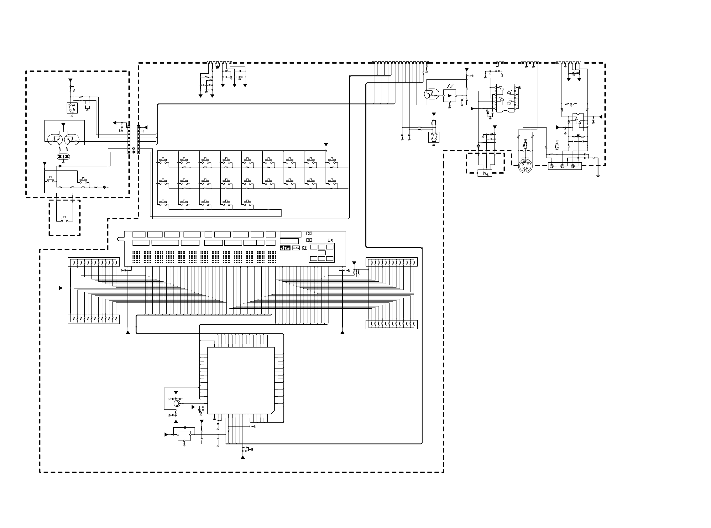
PC54
SURR. ENCODER
RLC(XC5X)
SC52
EC12E2420803 1A2
QC50 QC51
DTA114ES
UN4111
1
10K
3
10K
2
RC54 RC55
180 680
+5VL
SELECT
SC50
820
RC60
JUMPER
U ONLY
WA03AJ4040
RLC(XC6X)
STANDBY
+5VL
RC50 RC51
10k 10k
RC52
10k
RC53
10k
B
CC50 CC51
0 01 0 01
GND
C
3
GND
+5VL
DTA114ES
UN4111
1
0K
3
10K
2
3RED1GREEN
STANDBYUP GRADE
DC50
2
GL3ED8
GND
ENTER
SC51
RC58
RC57 RC59RC56
560 U 680
U JUMPER
OTHER JUMPER
OTHER 680
RC61
JUMPER
U ONLY
U ONLY
POWER
SC60
12
PC64
47k
RC05
1234567891011121314
S5B PH
CP15
JUMPER
RP07
534126
CVBS R
TO JS06(PS04)
VOLUME
AUX L
DGND
N.C
-12V
GND
1234567
AGND
12V
CP11 CP12
10 16V 10/16V
RP05
AGND
CP07
10/16V
1
2
CP03
3
47p
VGND
JUMPER
RP08
CP05
0 1
DUMMY
CP14
L
AGND
100
RP01
4
RP03
47k
CP01 CP02
1000p 1000p
12V
75
AUX R
+12V
07FMN SSTKA
+12V
RP06
47k0147k
CP08
10/16V
QP01
8
+VCC
7
-
6
+
5
NJM4558DD
VCC
RP04
AGND
47k
CP13
CP09
JP05
YKC21 5891
01
47p
AGND
CP04
100
RP02
JP06
YB00062270
CP06
EARTH
+12V
0 1
KEY2
SEL-
KEY2
SEL-
SEL+
10k
TO JU03(P604)
U-COM
KEY1
KEY0
SEL+
_S.BYLED
_WR T
_RSFL
KEY1
KEY0
_RSFL
WR TE
S.BY
CC26 CC27
0 01 0 01
GND GND
GND
VOL+
VOL-
SIOCLK
SIODATA
RCOUT
_CEFLD
_RSTFL
16151413121110987654321
RC41
DUMMY
GND
RC35
JUMPER
CEFLD
RSTFL
S OCLK
S ODATA
QC05
DTA114ES
UN4111
1
0K
1
3
47/6 3V
OUT
3
RPM6936 V4
RC39
10k
B
C
3
QC04
SC24
EC12E2430802
RLD(XP7X)
VCC
GND
2
GND
WA03AJ4070
AUX OPT
PC74
10K
2
+5VD
RC40
10k
10k
RC37
1A2
10k
RC38
GND
TO J803(P804)
SUPPLY
VKK
FL1
+5VL
JC02 JC03
765432
S7B PH
RC33
DUMMY
CC13
10/16V
CC14
0 01
GND
+5VD+5VL
+5VL
CC52
0 01
GND
JC50
08JQ ST
2
3
4
5
6
7
8
VC01
1
+5VL
2
GND
3
SEL+
4
SEL
5
S BY
6
WRIT
7
8
S8B XH A
+5VL
GND
SEL+
SEL
S BY
WRITE
JC01
HQ31606920
TV DVD VCR1 DSS/VCR2 AUX1 AUX2
SC14 SC15 SC16 SC17 SC18 SC19 SC20 SC21 SC22
7 1CH IN MEMORY CLEARSPK A/B DOWN
SC08 SC02 SC01SC07 SC03
RC28 RC29 RC31 RC32RC30
5 6k 2 7k 1 5k 1k2 2k
CM2071C
DISP MULTI AU TO TUNED ST V – OFF NIGHT PEAK ANALOG
AUTO
SURR
DIRECT DISC 6.1 MTX 6.1 SPKR AB EQ
62NL58NL57
61
GND
CC11
0 01
SLEEP
S3756S3655S154S253S352S451S550S649S748S847S946S1045S1144S1243S1342S1441S1540S1639S1738S1837S1936S2035S2134S2233S2332S2431S2530S2629S2728S2827S2926S3025S3124S3223S3322S3421S3520G119G218G317G416G515G612G911G10
F1
FL2
+5VD
GND
GND
CC20
RC34
JUMPER
100/6 3V
CC16
DUMMY
CC17
0 01
GND
CC15
DUMMY
CC18
CC22
CC21
100/50V
0 01
0 01
CC19
0 01
GND
GND
VKK
FL1 FL2
CD R TAPE CD
RC15 RC17RC16RC14RC13RC12
MULTI ROOMATT TUNER S D RECTMUTE A/D
SC11SC13 SC23 SC10SC12 SC09 SC04 SC05 SC06
RC22
2 2k
1 5k 8201k2 2k2 7k5 6k
RC24RC20 RC27RC25RC23RC21
1k5 6k 6808201 5k27k
UP FP MODE
ATT
DIGITAL
PCM
14G713G810
+5VL
RC18
560
RC26
560
RC19
680
SURROUND
DIGITAL
C
L
R
LFE
SL S SR
G118G137G146G15
G125G162F21NL
9
16FMN SSTK A
KEY0
KEY1
KEY2
10k
10k
10k
RC08
RC09
RC10
RC11
VKK
1234567891011121314
GND
CC12
0 01
+5VL
CC23
0 01
RC36
47
CC24
CC25
DUMMY
+5VD
TORX179L
TO JU07(P604)
U-COM
DGND
DUMMY
RP15
GND
GND
330
RP13
DP01
3 3V
GND
GND
RP12
10k
RC70 RC72RC71
JUMPER JUMPERJUMPER
OUT
1
JP70
OPT
DGND
AUX1 OPT
JP01 JP03JP02
12
S2B PH
CP22
DUMMY
RP14
JUMPER
QP02
TC74VHC08F
GND
8
9
10
11
12
13
VCC
14
CP21
0 1
+5VD
CP20
100/6 3V
CP19
JUMPER
01
3
VCC2GND
TO JL04(PL04)
VIDEO
AUX1 C
GND
AUX1 CVBS
VGNDVGND DGND
7
GND
6
5
4
3
2
1
CP16
VGND
JUMPER
RP11
CP18
DUMMY
JUMPER
RP10
RP09
75
75
5
132
4
Y/C
GND
AUX1 Y
12345
CP 7
JP04
YKF51 5584
VKK
PC04
RLC(XCXX)
RLD(XPXX)
1234567891011121314
47k
RC06
FRONT DISPLAY
AUX
MK1
MK2
+5VD
S10
S9S8S7S6S5S4S3S2S1
T15
T1T2T3T4T5T6T7T8T9
S35
S34
S33
S32
S31
S30
S29
S28
S27
S26
S25
S23
S22
S21
T1
32T131
S3530S3429S3328S3227S3126S3025S2924S2823S2722S2621S2520S2419S2318S2217S21
T2 S20
T2
33
T3
T3
34
T4
T4
35
T5
T5
36
T6
T6
37
T7
T7
38
T8
T8
39
T9
T9
40
T10
T10
41
T11
T11
T16
42
T12
12
10/50V
T12
43
T13
T13
44
T14
T14
45
T15
T15
46
T16
47
VFDP
48
CC04
CC05
0 01
49
GND
+5VD
GND
CC07
390p
RC02
UMMY
CC28
CC06
DUMMY
0 1
+5VD
CC02
CC01
DUMMY
0 01
GNDGND
2
3
QC02
VKK
C2458
1
C1740S
C3199
RC01
10k
CC03
0 01
VKK
DUMMY
DC01
12
IN OUT
GND
QC03
3
DUMMY
GND
QC01
NJU3430
HC10220090
Vss
OSC151OSC252RST53CS54CLK55SI56RS57VDD58P159MK260MK161S162S263S364S4
50
RC03
68k
100
GND
RC04
CEFLD
SIODATA
SIOCLK
_RSTFL
CC09
0 01
GND
CC10
100 6 3V
S24
S20
16
S19
S19
15
S18
S18
14
S17
S17
13
S16
S16
12
S15
S15
11
S14
S14
10
S13
S13
9
S12
S12
8
S11
S11
7
S10
S10
6
S9
S9
5
S8
S8
4
S7
S7
3
S6
S6
2
S5
S5
1
S3S2S1
MK1
MK2
S4
GND
CC08
100p
RSFL
GND
+5VD
T10
T16
T11
T12
T13
T14
FL1FL2
1234567891011121314
47k
RC07
S35
S34
S33
S32
S31
S30
S29
S28
S27
S26
S25
S24
S23
S22
S21
S20
S19
S18
S17
S16
S15
S14
S13
S12
S11
1615
Page 13
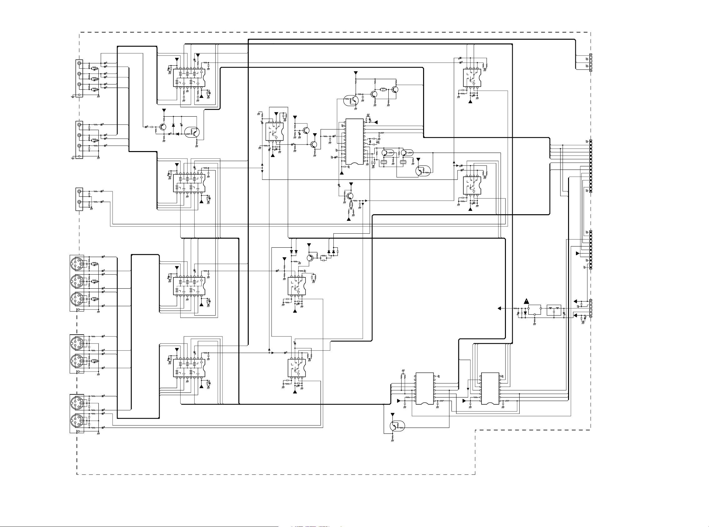
TV
DVD
VCR1 IN
VCR1 OUT
IN
DSS/VCR2
OUT
MONI_OUT
MULTI_OUT
TV M
10/50V
DVD M
CF09
CF10
0 01
100/10V
GND
QF01
NJM2595D
MULTI SEL
VCR1 M
VCR2 M
+5VL
RL81
10
QL80
CL81
1
JUMPER
3
CL80
A1048
A933
RL80
A12672
220k
CL82
RL82
2 2/50V
220
GND
TV
DVD
CL18
CL17
0 01
100/10V
GND
QL01
NJM2595D
CVBS SEL
VCR1
VCR1 OUT
VCR2
VCR2 OUT
JL01
5
RL01
75
6
3
RL03
75
4
1
RL05
75
2
7
JL02
5
6
3
4
1
2
7
JL03
1
2
3
4
RL02
JUMPER
CL02
RL04
JUMPER
CL04
RL06
JUMPER
CL06
CL10
47p
RL07 RL08
75
JUMPER
CL08
CL12
47p
CL14
68p
CF06
68p
GND
DUMMY
DUMMY
DUMMY
RL09
DUMMY
RL10
RL11
RF01
CF01
10/50V
TV M
DVD M
VCR1 M
VCR2 M
TV
DVD
VCR1
VCR1 OUT
VCR2
VCR2 OUT
10/50V
CL01
10/50V
CF02
10/50V
CL03
10/50V
CF03
10/50V
CL05
GND
CL09
470/6 3V
75
10/50V
CF04
10/50V
CL07
470 6 3V
CL11
75
GND
CL13
470/6 3V
75
CF05
470/6 3V
75
AUX1
MSEL VC
MSEL_VD
5VV
DL80
DL81
5VV
RF05
10 50V
JUMPER
CF14
75
75
GND
CF11
47p
RF02
RF03
GNDGND GND
CL83
10 50V
1
10K
3
10k
QL81
2
DTA114ES
UN4111
RL83
10k
GND
AUX1
CL19
10/50V
GND
MSEL VB
MSEL VA
+5VV
75
RF04
CF13
47p
12345678
GND
CF08
100 10V
161514131211109
CF07
0 01
+5VV
GND
CF12
47p
TV_AUTO
75
RL12
12345678
CL20
47p
GND
CL16
100 10V
161514131211109
CL15
0 01
+5VV
GND
AUX1
+5VV
RL29
RL30 RL31
4 7k
1k 1k
RL23
QL14 QL15
C2458 C2458
QL13
DTC114ES
UN4211
3
CL54
+5VV
0 01
RL13
1M
GND
CL21
10 50V
QL02
NJM2535D
OSD SEL
H Y/C
RX21
L CVBS
1M
GND
CX35
10 50V
AUX1
+5VV
BYPASS OSD
+5VV
RL44
1M
1234
GND
RL14
12k
RL15
BUFF
10k
CL25
4 7 50V
8765
CL22
0 01
RL16
100k
CL23
GND
100/10V
GND GND
GND
C2458
QL06
C31992
C1740S
3
+5VV
1
CL24
10/50V
2
3
QL07
C2458
1
C3199
RL17
C1740S
470
GND
GND
CL26
1 50V
RL18
CL27
220
1200p
GND
GND
CL28
1 50V
GND
23 22 21 20 19 18 17 16 15 14 13
24
CL29
0 01
+5VV
CL37
10/50V
RL24
10k
RL25
DUMMY
GND
RL45
DUMM
5VV
C3199
RL32
2
C1740S
10k
3
2
CL39
1
0 022u
10k
10k
1
QL03
LC74781
QL11
C2458
C3199
75
CL38
47p
RL46
JUMPER
VDD2
DATA
SCLK
CHARA
OSC O
OSC I
BLNK
CNT1
XOUT
VSS1
GND
GND
CL30
0 01
10 11 12
CS
9
8
7
6
5
4
3
XIN
2
1
GND
CL35 CL36
N S 15p
U F 22p
CVBS
MULTI
Y
GND GND
CL31
100/10V
RL22
CL33
24p
LL01
33uH
CL34
22p
RL19
GND
N S 15p
U F 22p
GND
CV O
NC
CV IN
VDD1
SY IN
SEPC
SEP O
SEP I
CNT2
CNT3
RST
VDD1
GND
+5VV
2
C1740S
3
RL28
1
RL27RL26
DUMM220
GND
+5VV
1M
1k
CL40
47p
JUMPER
CL32
DUMMY
GND
GND
2
1
14 31818MHz
3
1
RL34RL33
10k56
QL08
DTC114TS
UN4215
N S ONLY
3
10k
RL20
DUMMY
XL01
GND GND
2
RL38
JUMPER
U F
17 31818MHz
C3199
C1740S
2
XL02
N S ONLY
1
QL09
DTC114TS
UN4215
N S ONLY
10k
RL21
DUMMY
VSYNC
DATA
CLK
CEOSD
3
+5VV
QL10
DTA114ES
UN4111
N S ONLY
1
10K
3
10K
2
BYPASS
OSD
M_OSD
MV_MUTE
CF16
10/50V
CF15
10/50V
CF19
0 01
RF08
1M
GND
CL41
10/50V
CL42
10/50V
CL45
0 01
RL35
1M
GND
RF06
1M
RF07
1M
1234
GND
QF02
NJM2244D
75 DRV
8765
CF17
0 01
CF18
100/1 V
GND
+5VV
DATA
CLK
VSYNC
CEOSD
TV AUTO
RL36
1M
RL37
1234
1M
GND
QL04
NJM2244D
DRV
75
8765
CL43
0 01
CL44
100/1 V
GND
+5VV
CVBS OSD
CVBS OSD
Y OSD
DATA
CLK
JL04
S5B PH
AUX1
5
AUX1 CVBS
4
GND
GNDGND GNDGND
JL05
GND
3
2
1
15
14
13
12
11
10
9
8
7
6
5
4
3
2
1
AUX1 C
GND
AUX1 Y
GND
OSDDATA
OSDCLK
VSYNC
CEOSD
TV AUTO
CVBS OSD
TXD
Y OSD
RTS
TO J604(P604)
CEEX
RXD
NC
CTS
GND
TO JP02(PC04)
FRONT
U-COM
AUX1 C
AUX1 Y
15FMN BTK A
CEEX
TV
DVD
VCR1 IN
VCR1 OUT
DSS/VCR2
IN
DSS/VCR2
OUT
MONI_OUT
JX01
YKF51 5514
521378
C
4
Y
C
10 612 13
9
Y
C
15 1116
14
JX02
YKF51 5510
Y
4 5213
RX10
Y
78
9 10 611
JX03
YKF51 5510
Y
5213
C
4
Y
C
10 611
78
9
PL04
RVC(XLXX)
RVS(XXXX)
RVM(XFXX)
GND
GND
11
JL06
YJ07060290
11FMN BTK A
JL07
S5B EH
CL51
0 01
GND
GND
GND
10
CL53CL52
10/50V0 01
9
8
7
6
5
4
3
2
1
1
2
3
4
5
CTS
CPMUTE
RXD
COMP SEL
RTS
5VV
TXD
GND
+5VV
GND
+5VV
GND
12V
GND
+5VL
TO JF54(PF04)
COMPONENT
TO J981(PY04)
DIGTAL INPUT
SEL VB
SEL_VA
SEL VC
SEL_VD
TV Y
10/50V
RX01
CX01
75
RX03
JUMPER
CX03
RX02
DUMMY
75
CX02
10/50V
10/50V
CX04
RX04
75
RX06
JUMPER
CX06
RX05
DUMMY
CX05
75
10/50V
CX07
10/50V
RX07
RX09
75
JUMPER
CX09
DUMMY
RX08
CX08
10/50V
75
GND
RX13
VCR1 OUT Y
75
CX13
470/6 3V
CX15
47p
CX16
47p
CX14
10/50V
75
RX14
75
CX10
RX12
10 50V
JUMPER
CX11
CX12
10 50V
DUMMY
75
RX11
GND
75
RX15
VCR2 OUT Y
CX17
CX19
470/6 3V
47p
CX20
CX18
47p
10 50V
75
RX16
75
RX17
CX21
CX23
470/6 3V
68p
CX24
CX22
68p
10 50V
75
RX18
GND
DVD Y
VCR1 Y
VCR2 Y
TV C
DVD C
VCR1 C
VCR1 OUT C
VCR2 C
VCR2 OUT C
TV C
DVD C
CX28
100/10V 0 01
QX01
NJM2595D
C SEL
VCR1 C
VCR1 OUT C
VCR2 C
VCR2 OUT C
TV Y
DVD Y
CX33
100/10V
QX02
NJM2595D
Y SEL
VCR1 Y
VCR1 OUT Y
VCR2 Y
VCR2 OUT Y
CX47
0 50V
5VV
CX27
GND
GND
CX48
0 50V
5VV
CX32
0 01
GND
GND
SEL VB
SEL_VA
SEL VE
AUX1 C
AUX1 Y
SEL VE
SEL VD
SEL_VC
SEL VB
SEL VA
AUX1 C
75
RX19
CX29
47p
12345678
GND
CX26
100 10V
161514131211109
CX25
0 01
+5VV
GND
AUX1 Y
75
RX20
CX34
47p
12345678
GND
CX31
100 10V
161514131211109
CX30
0 01
+5VV
GND
SEL VE
SEL_VC
SEL_VD
OSD
BYPASS
OSD SEL
V_MUTE
2
121
+5VV
RX24
DUMMY
RX22
3 3k
RX23
CX36
2 2k
10/50V
GND
CX37
0 01
GND
+5VV
CX41 RX28
10 50V 1M
CX42
0 01
RX29
1M
GND
+5VV
OSD INT
75
10/50V
75
+5VV
RX31
10k
DX02DX01
1
QX05
3
A1048
A933
A1267 2
GND
RX32
1k
GND
1234
CX45
0 01
CLAMP
GND
QX03
DRV
NJM2264D
8765
CX38
0 01
CX39RX26
100 10V1M
GND
CX40
RX27
1M
1234
GND
QX04
NJM2244D
DRV
8765
CX43
0 01
CX44
100 10V
GND
BLNK
OSD_SEL
DX03
CX46
RX30
1000p
10k
DX04
CX49
100p
RX25
1M
Y_OSD
GND
QL05
74HC4094D
8
GND
7
Q4
6
Q3
5
Q2
4
Q1
3
CLK
2
DATA
1
CE
GNDGND
9
RL47RL48
QS
DUMMYDUMM
10
SEL VD
SEL VC
SEL VA
SEL VB
+5VV +5VV
SEL_VE
+5VV
QL12
1
2
RL41
10k
GND
QS
11
Q8
12
Q7
13
Q6
4
Q5
RL39
10k
5
OE
6
VCC
CL46
0 01
COMP SEL
DTA114ES
UN4111
10K
3
10k
GND
OSD INT
OSD SEL
V MUTE
CL47
1000p
M_OSD
MSEL VB
MV_MUTE
NTSC/PAL
9
10
11
12
13
14
RF09
15
10k
16
CF20
0 01
GND GND
V MUTE
_NTSC/PAL
5VV
QL16
NJM7905FA
RL42
JUMPER
32
CL50 CL49
100/10V 0 01
OUT IN
2
GND
1
DL01
1D3
5VV
MSEL VC
MSEL_VD
MSEL VA
8
GND
QS
Q S
Q8
Q7
Q6
Q5
OE
VCC
QF03
Q4
Q3
Q2
Q1
74HC4094D
CLK
DATA
CE
GND
7
6
5
4
3
2
RF10RL40
100100
1
CF21
1000p
12
1
RL43
JUMPER
GND
LL02
3
COMP MUTE
CL48
10/50V
+5VV
+5VL
CLK
DATA
CEEX
CVBS
Y/C
MULTI
17 18
Page 14
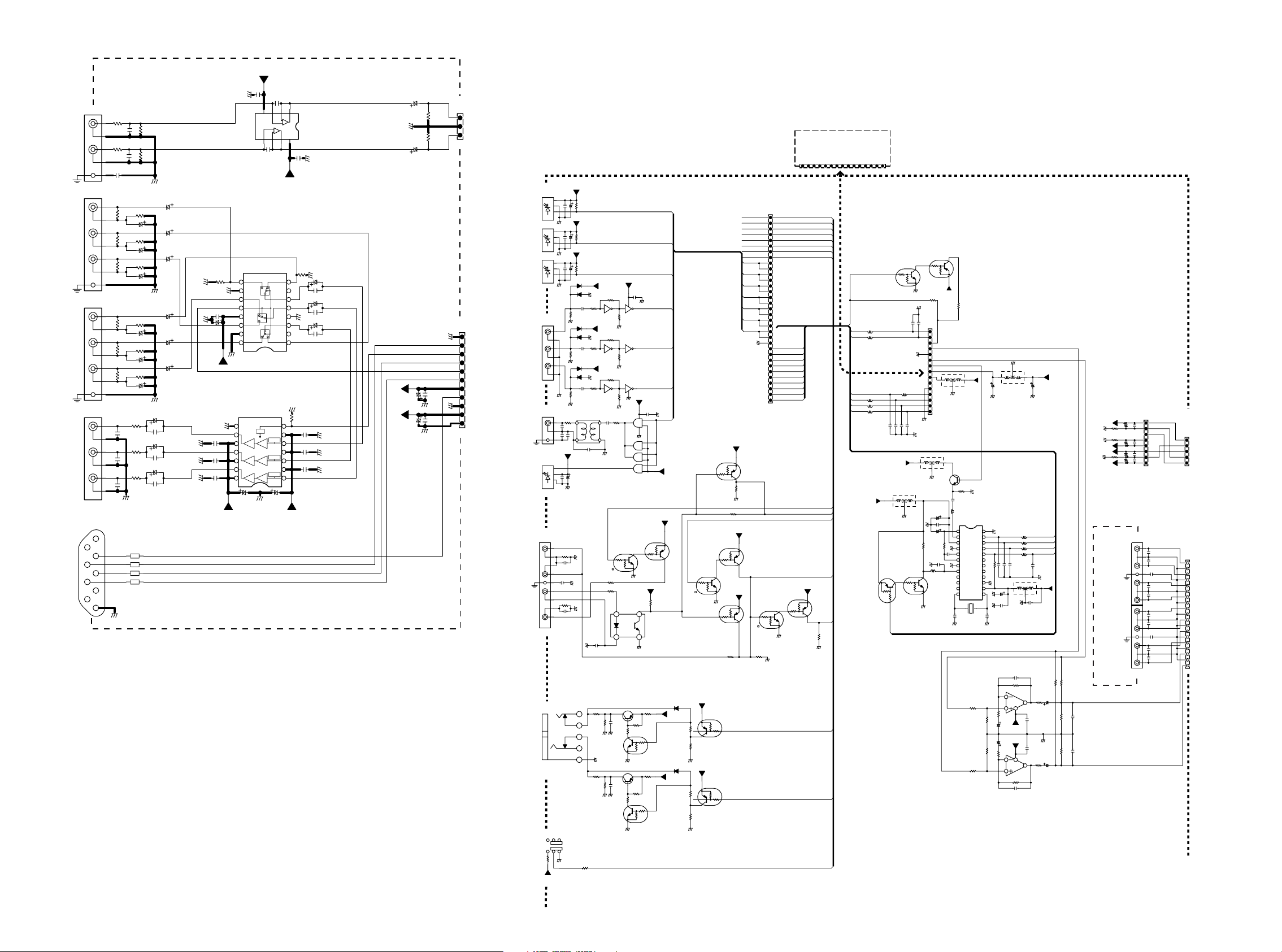
TUNER
(F ONLY)
DVD
DSS/VCR2
MONITOR_
OUT
DTR
CTS
RS232C
RTS
5VV
CS38
DUMMY
CS34
JUMPER
A-GND
JS71
R
L
JF51
Y
C
B
C
R
JF52
Y
C
B
C
R COMP_SEL
JF53
Y
C
B
C
R
JU11
DZ101A1 B2
N.C
1
6
TXD
2
7
RXD
3
8
DSR
4
N.C
9
GND
5
5
6
3
4
1
2
7
5
6
3
4
1
2
7
5
6
3
4
1
2
1
3
2
4
5
RS72
100
RS71
100
CS97
JUMPER
RF51
75
RF53
75
RF55
75
RF57
75
RF59
75
RF61
75
CF65
DUMMY
CF68
DUMMY
CF71
DUMMY
CS32 RS74
470p 82k
CS31 RS73
470p 82k
RF52
CF52
RF54
CF54
RF56
CF56
RF58
CF58
RF60
CF60
RF62
CF62
RF63
75
RF64
75
RF65
75
GND
LU81
LU82
LU83
LU84
JUMPER
DUMMY
JUMPER
DUMMY
JUMPER
DUMMY
JUMPER
DUMMY
JUMPER
DUMMY
JUMPER
DUMMY
JUMPER
JUMPER
JUMPER
JUMPER
A GND
GND
GND
CF66
CF69
CF51
47/10V
CF53
47/10V
CF55
47/10V
CF57
47/10V
CF59
47/10V
CF61
47/10V
CF63
CF64
470/6 3V
CF67
470/6 3V
CF70
470/6 3V
0 01
0 01
0 01
GND
GND
GND
GND
GND
CF72
CF73
47/10V
CF83
0 01
CF84
0 01
CF85
0 01
RF66
1M
0 01
+5VV
+5VV
GND
GND
GND
10
11
12
13
14
8
9
QS10
DUMMY
9
10
11
12
13
14
15
16
QF52
NJM2581D
CF86
100/10V
QF51
NJM2584D
PF04
CLAM P
BIAS
BIAS
75D
75D
GND
123+4
NJM4558DD
+
8765
CS33
JUMPER
CS37
DUMMY
+5VV
COMPONENT
RVP(XFXX)
RF67
1M
8
7
6
5
4
3
2
1
GND
RF68
DUMMY
7
BIAS
BIAS
BIAS
CF87
100/10V
CF80
6
0 01
5
CF81
4
0 01
3
CF82
2
0 01
1
REF
6dB75D
6dB
6dB
5VV
GND
A-GND
GND
CF74
CF75
CF76
CF77
CF78
CF79
GND
GND
GND
47/10V
0 01
47/10V
0 01
47/10V
0 01
5VV
+5VV
CF88
10/50V
CS36
JUMPER
A-GND
CS35
JUMPER
CF90
10/50V
GND
GND
RS76
DUMMY
RS75
DUMMY
CF89
0 01
CF91
0 01
GND
TO JE11(PS04)
FUNCTION
JS72
3
TUNER R
2
GND
1
TUNER L
S3B EH
TO JL06(PL04)
CVBS_Y/C
JF54
1
GND
GND
2
CTS
3
_CPMUTE
4
RXD
5
6
RTS
7
-5VV
8
TXD
9
GND
GND
10
+5VV
11
GND
11FMN BTK A
Multi-Remote OUT
DIGIN1
DIGIN2
DIGI3
DIGIN4
DIGIN5
DIGIN6
RC-5 IN/OUT
Multi-Remote IN
DC OUT 1
DC OUT 2
JA01
TORX179L
JA02
TORX179L
JA03
TORX179L
JA04
JA07
TOTX179L
JA51
LGA6502 0150
JA50
RA64
12k
+5VL
TUNER MODULE
CEDCLDOGND
+5VD
CA01
0 01
CA02
3
47uF/25V
2
RA01
DAMMY
1
+5VD
CA03
D GND
0 01
CA04
3
None
2
RA02
DAMMY
1
+5VD
D GND
CA06
0 01
3
CA05
47uF/25V
2
RA03
DAMMY
1
DA01
D GND
5
6
3
4
1
2
D GND
JA06
RA16
75
1
CA11
62p
2
3
CA12
CA13
0 01
0 01
+5VD
3
CA16
2
1
0 01
D GND
5
47
RA70
6
8
0 01
CA56
7
CA53
9
load(0)
1
2
RA68
4
CA52
3
D GND
D GND
D GND
47
0 01
CA17
RA04
75
CA08
RA08
75
CA09
RA12
75
47uF/25V
DA02
CA07
RA05
0 1
DA03
DA04
0 1
RA09
DA05
DA06
RA13
0 1
LA01
Puls Trans
4
6 1
CA14
470p
D GND
D-GND
D-GND
D-GND
D-GND
1k
D-GND
1k
D-GND
1k
CA54
0 01
+5VD
RA06
12
74HCU04A
+5VD
RA10
34
74HCU04A
+5VD
RA14
56
74HCU04A
CA15
D GND
RA67
RA66
spec load 270ohms
10 1/6W
RA50
6
RA52
10k
5
D GND
2
3
D-GND
1
10 1 6W
RA51
RA53
10k
D GND
654
SA50
SPUN
321
D GND
RA65
1k
PD04
RDS
DI[1]
DI[2]
+5VD
CA10
100k
4
13 12
QA01
QA01
RA07
4 7k
D GND
100k
11 10
QA01
QA01
74HCU04A
RA11
4 7k
D GND
100k
QA01
74HCU04A
9
7
QA01
RA15
D GND
4 7k
D GND
QA02
74HC08
8
RA17
0 1
27
3
QA02
74HC08
11
QA02
74HC08
6
QA56
KRC102M
3
D GND
220
220
QA58
PC817
44ma 12V
2SA970
QA50
231
CA50
0 01
RA54
6 8k
D GND
2
1
D GND
2AS970
QA51
231
CA51
0 01
D GND
RA55
6 8k
2
1
D GND
DI[3]
0 01
D GND
DI[4]
74HCU04A
DI[5]
DI[6]
8
+5VD
CA18
0 01
14
D GND
9
SPD FO
10
7
D GND
2
1
12
13
5
4
QA02
2
RA56
22k
QA52
KRC102M/UN4211/DTC114ES
RA57
22k
+5VD
74HC08
+5VL
1
3
2
QA57
KRA102M
1
+5VL
RA69
18k
41
32
D GND D GND
DA50
RA58
+12V
2 2 1 4W
3
DA51
RA59
+12V
2 2 1 4W
3
QA53
KRC102M
3
3
QA60
KRC102M
D GND
+5VD
QA54
KRA102M
1
RA60
1k
2
RA62
Dummy
D GND
+5VD
QA55
1
KRA102M
RA61
1k
2
RA63
Dummy
D GND
QA64
DAMMY
KRA102M
QA59
3
2
1
3
QA61
KRA102M
RA71
M RC OUT
M RC N
RC OUT
RC IN
DC OUT1
DC OUT2
MD2
SPDIFO
DI 1]
DI 2]
DI 3]
DI 4]
DI 5]
DI 6]
D GND
TU SD
TU ST
TU MUTE
CE TU
KILL RDS
CE RDS
TUDOUT
TUCLK
TUD N
RDSD N
+5VL
1
2
RA75
DAMMY
D GND
0
RA76
+5VL
1
2
+5VL
1
3
2
QA62
KRC102M
220
RA72
3
3
33
32
31
R
30
29
28
27
26
25
24
23
22
21
20
19
18
17
16
15
14
13
12
11
10
47k
D GND
DIGOUT
DIG1 IN
DIG2 IN
DIG3 IN
DIG4 IN
DIG5 IN
DIG6 IN
DIG GND
9
8
7
6
5
4
3
2
1
JA08
33FMN BTK A
New
D GND
M RC OUT
M RC IN
RC OUT
KILL R
RC IN
DC OUT2
DC OUT1
MD2( WRTI)
TU SD
TU ST
TU MUTE
CE TU
KILL RDS
CE RDS
TUDOUT
TUCLK
TUD N
RDSDIN
M RC OUT
M RC IN
RC OUT
KILL R
+5VL
1
3
2
2
QA63
KRA102M
1
RA73
47k
DC OUT1
DC OUT2
MD2( WRTI)
RC IN
AT01
FM FOUT
VCC2(+5V)
VCC1(+12V)
DETOUT
LOUT
GND
ROUT
MUTE
TUNED
STEREO
2
3
QT02
KRC102M
2
3
A GND
A GND
TU_MUTE
100ohm
LT08
TU ST
100ohm
TU SD
LT07
TUDIN
100ohm
LT03
TUCLK
100ohm
TUDOUT
LT02
100ohm
CE TU
LT01
+5VD
Q904
KRA102M
1
100p
CT05
A GND
100ohm
LT04
22p
100p
100p
100p
CT04
CT03
CT01
CT02
1
+12V
10ohms
L901
3
D GND
2
3
Q903
KRC102M
3
K LL RDS
1
QT04
KRA102M
1
+5VD
33k
RT02
2 2k
RT01
100p
CT06
JT01
1
2
3
4
5
6
7
8
9
10
11
12
13
14
15
15FE BT
A GND
A-GND
10ohms
L913
3
D GND
12
C901
10 50V
C902
0 01
C903
D-GND
10 50V
47k
100k
R902
C904
560p
C905
1000p
D-GND
0ohms
L912
2
1
D GND
RTU
A GND
12
+5VD
LT06
CT07
10/50V
SR ONLY
24
D-GND
23
22
21
20
19
10k
100p
18
17
R904
C910
16
15
D-GND
14
13
C912
D GNDD-GND
10 50V
C913
0 01
22p
C914
D GNDD GND
2
3
47k47k
R953R954
C955 R957
4 7/50V 15k
15k 4 7/50V
6
R958 C956
5
3
10ohms
CT08
A GNDA GND
RTR
100ohm
L906
CE RDS
100ohm
L905
TUDOUT
100ohm
L904
TUCLK
100ohm
L903
RDSDIN
100p
100p
22p
C907
C909
C908
10ohms
L911
D-GND
12
C953
R955
OP AMP1 2
12V
+12V
OP AMP2 2
R956
C954
U Only
D-GND
100p
10k
NJM4558DD
4
8
NJM4558DD
10k
100p
Uxxx
+5VD
3
C911
DAMMY
Q951
R959
220
1
C957
4 7/50V
0 01
C959
A GND
0 01
C960
R960
7
220
C958
Q951
4 7/50V
+12V
J980
C980 C984
100 16V 001
+5VL
R980
R981
0
0
100 16V 001
C982
100/16V
C983
100/16V
FL
FR
SL
SR
SBL
SBR
CNT
SW
C981 C985
J971
C986
0 01
C987
0 01
J970
YT02041370
8
7
6
5
4
3
2
1
B8B PH
4
6
5
7
1
3
2
4
6
5
7
1
3
2
YT02041370
+5VVG
J981
+5VV
B5B EH
+5VDG
+5VD
12V
+12VG
+12V
C971
470p
C972
470p
C988
0 01
C973
470p
C974
470p
C975
470p
C976
470p
C989
0 01
C977
470p
C978
470p
5
4
3
2
1
19FMN BTK A
J972
19
18
17
16
15
14
13
12
11
10
9
8
7
6
5
4
3
2
1
+5VL
+12VG
+5VVG
+5VV
GND
FR
GND
GND
SR
GND
GND
SBR
GND
CNT
GND
SW
GND
GND
12V
FL
SL
SBL
TU L
TU R
+5VL
D GND
D GND
+5VD
12V
A GND
R982
+12V
0
PREOUT
U Ony
47
47
R963
R964
47k
470p
R961
C961
C962
47k
470p
R962
12
10ohms
LT05
3
A GND
12
Q902
2SC2458
2
3
1
10k
R903
D GND
0ohm 330p
L902 C906
Q901
LC72722
1
VREF
SYR
2
MPXIN
CE
3
VDDA
DI
4
VSSA
D-GND
D-GND
CL
5
FLOUT
DO
6
C N
RDS ID
7
T1
SYNC
8
T2
T7
9
T3
T6
10
T4
VSSD
11
T5
VDDD
12
XOUT
X N
X901
27p
4 322MHz
C915
R951
47
R952
47
R901
2019
Page 15
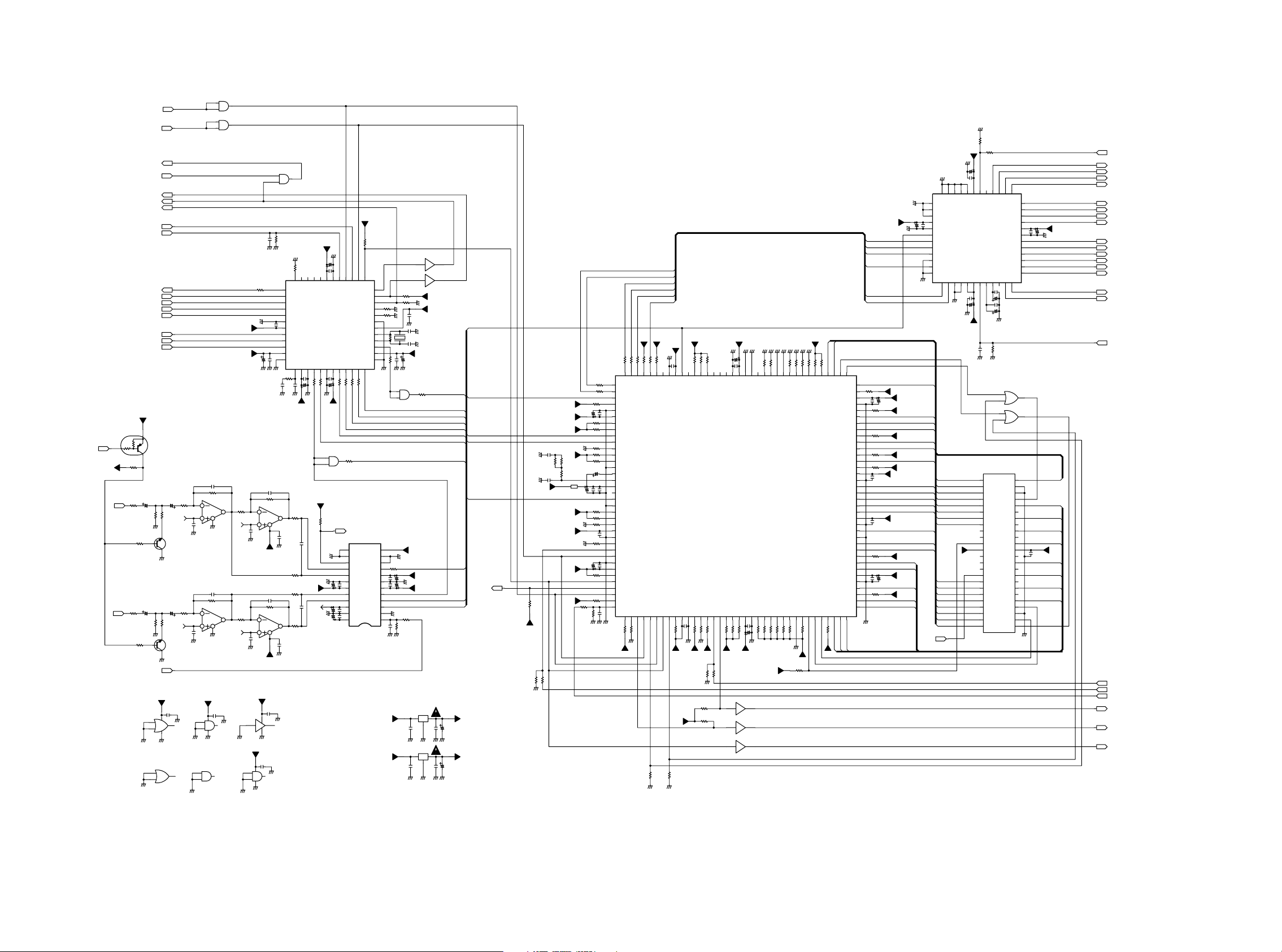
P604-1/2
13
11
DSPCLK
DSPDOUT
ERMUTE
D A
D R INT
RERR
XSTATE
CEDIR
XMODE
SPD FO
SPDIFI[0]
SPDIFI[1]
SPDIFI[2]
SPDIFI[3]
SPDIFI[4]
SPDIFI[5]
SPDIFI[6]
+5VD
QK05
DTA114EU
ATT
LT
RT
1
3
2
-15V
RK21
1M
CK03
CK01
RK01
6 8k
RK02
6 8k
22/6 322/6 3
RK17
RK15
2 7k
100k
B AS
GND
E
1
RK19
2 2k
B
3
QK03
C
2
2SC4213
GND
CK02
CK04
22/6 3
22 6 3
RK18
RK16
2 7k
100k
B AS
E
1
RK20
GND
2 2k
B
3
QK04
C
2
2SC4213
GND
RSTADC
+3 3V
C625
0 1
14
4
GND
5
6
7
GNDGND
Q603
74VHCT32A
1
3
2
Q603
74VHCT32A
GND
12
QR02
TC74VHCT08AFT
10
9
QR02
TC74VHCT08AFT
150p
CK05
5 6k
RK05
RK03
QK01
6
4 7k
2115M
7
OP AMP1/2
4
5
CK11
0 1
GND
GND
150p
CK06
5 6k
RK06
RK04
QK02
6
4 7k
2115M
7
OP AMP1/2
4
5
CK12
0 1
GND
+3 3V
CR18
0 1
14
4
6
GND
5
7
GND
GND GNDGND
QR02
TC74VHCT08AFT
4
6
5
QR03
TC74VHCT08AFT
GND GND
8
1
3
2
QR02
TC74VHCT08AFT
CD02
LRCLKO
AUDATA[0]
BCKO
AUDATA[1]
AUDATA[2]
AUDATA 3]
R628
R627
R626
R625
R624
C606
C605
R623
C603
C604
R622
10k
01
10k
10k
10k
10k
0 1
10k
0 1
22u/6 3
10k
22/6 3
+3 3V
+3.3V
C607
+3.3V+3.3V
C608
+3 3V+3.3V +3.3V+33V+3.3V+3.3V
+3.3V+3.3V
+3 3V
GND
CR17
22u/6.3
41
42
40
DGND
XMODE
100
RR05
+3 3V
3
RR18
13
14
GND
15
16
17
0 1
18
19
20
22/6 3
21
22
23
24
CK37
0 1
CK39
0 1
3.3k
RR15
39CE38DI37
CL
DO
36
RERR
35
INT
34
CKST
33
AUDIO/VO
32
EMPHA/UO
31
DGND
30
DVDD
29
XIN
28
XOUT
27
XMCK
26
DVDD
25
DGND
SDIN
GND
24
100
100
100
RR07
RR08
RR06
33
OVFL
QK30
CS5361-KS ES
M012DIF
M1
HPF
OVFL
DIV
A NL+
SDOU
A NL
VL
GND
GND
VA
VD
A NR
MCLK
A NR+
SCLK
VCOM
LRCK
REFGND
M/ S
F LT+
RST
RR12
10k
10k
RR11
11
10
9
8
7
6
5
4
3
2
1
GND
RR10
1M
100
GND
CR10
RR09
0 10 1
12
13
TC74VHCT08AFT
27
RK32
GNDGND
RK30CK30
10k470p
+3.3V
+5VD
RR14
10k
RR13
GND
0.1
GND
CR14
GND
XR51
12 288MHz
GND
CR11
22u/6 3
QR03
GND
RK31
GND
C680
C683
GND GNDGND
12
QR04
TC74HCT7007AF
34
QR04
TC74HCT7007AF
10k
+3.3V
GND
+3.3V
CR13
22p
GND
CR12
GND
22p
+3 3V
11
RR19
+3.3V
+3.3V
GND
+3.3V
5 6k
TA48025F
Q680
0.1
TA48033F
Q681
0.1
GND
XMCK
33
ADDATA
ADLRCK
ADBCK
RDATA
RLRCLK
RBCK
RMCK
ADDATA
CK34
CK33
22/6 3
0 1
CK31
CK32
0 1
22/6 3
ADBCK
ADLRCK
13
2
C682
100/6 3
0.1
C681
GNDGND GNDGND
13
2
C685
100/6 3
0.1
C684
AUDATA[0]
AUDATA[1]
LRCLKO
AUDATA[2]
AUDATA[3]
BCKO
RMCK
C611
+2 5V
+2 5V +25V
0 1
+2 5V
10k
33
10k
R643
R642
R641
R640
02
103
104
05
GPIO4
GPIO3
SCLK0
HDATA4,
HDATA3,
AUDATA2
XMT958A
AUDATA3,
GPIO193INTREQ,
ABOOT4FA1,FSCDIN5GPIO206FA0,FSCCLK7FHS2,FSCDIO
10k
R672
GND GND
GND
99
101
VSS2
GPIO28
AUDATA4
FSCDOUT,FGPIO9
GPIO219FDAT7,
8
10k
R603
10k
R673
10k
R639
97
98
MCLK00VDD2
SCLK1
FGPIO710VDD611VSS612FHS0,FWR FDS,
0 1
3 3k
C600
R604
+2 5V+25V
+2.5V
10k
R638
96
GPIO5
HDATA5,
FGPIO1013FHS1,FRD,FR/W,
3 3k
R605
GND
R609
R602
10k
R637
95
GPIO6
HDATA6,
FGPIO1114FDAT6,
10k
R606
+2 5V+2 5V
10k
R607
GND
333333
R645
R644
106
07
108
LRCLK0
R646
33
109
AUDATA1
R647
33
110
RBCK
C612
C613
0 1
22u/6 3
+2.5V
dummy
+2.5V +2 5V
C616
1200p
R619R675
1 5k
R654
C615
1 5k
68p
+2.5V
C618
47u/4
C621
22u/6 3V
+2.5V +2.5V+2.5V +2.5V
+2.5V
R665
5 6k
5.6k
R659
RLRCLK
RDATA
GND
GND
XMCK
HINBUSY
10k
R662
+2 5V
10k
R660
GND
+2.5V
+3.3V
AUDATA0
111
CMPCLK
FSCLKN2
10k
R648
112
HDATA2
GP O2
113
VSS3
114
VDD3
10k
R649
115
HDATA1
GP O1
116
HDATA0
GP O0
10k
R650
117
CMPREQ
FLRCLKN2
118
CMPDAT
FSDATAN2
10k
R651
119
FLRCLKN1
10k
R652
120
WR DS
GP O10
121
RD R/W
GP O11
10k
R653
122
PLLVSS
C614
2 2u 50
123
FILT2
124
FILT1
C617
C687L600
125
PLLVDD
126
CLKOUT XTALO
0 01
1
127
CLKIN XTALI
128
CLKSEL
10k
R655
129
CS GPIO9
10k
R656
130
A0 GPIO13
10k
R674
131
FSDATAN1
GND GND
132
VDD4
C619
133
0 1
VSS4
10k
R658
134
FSCLKN1
GND
STCCLK2
135
SCS
136
SCDIN
C620
137
0 1
VSS5
138
VDD5
139
A1 GPIO12
10k
R661
140
SCDOUT
SCDIO
141
H NBSY
GP O8
142
SCCLK
3 3k
R663
143
UHS2 CS OUT
GP O17
144
RESET
UHS0
GP O18
UHS1,
1
2
GND
GNDGND
C622
R664
10k
3 3k
3 3k
0 1
R600
R601
GND
22u/6 3
C610
C609
0 1
+2 5V
GND
GNDGND GNDGND
88
90
92
93
94
VDD191VSS1
GPIO7
GPIO30
GPIO29
HDATA7,
AUDATA7,
AUDATA6,
AUDATA5,
XMT958B,GP O31
Q600
CS494002/CS494003
FGPIO615FCS16FINTREQ17FDBCK18FDAT5,
FGPIO519FDAT4,
FGPIO420VDD721VSS722FDAT3,
+2 5V
+2 5V
C601
0 1
10k
10k
10k
C602
22u/6 3
5.6k
R610
R612
R611
R608
TC74HCT7007AF
QR04
3 3k
56
3 3k
TC74HCT7007AF
QR04
98
QR04
TC74HCT7007AF
11 10
GN DG N D G NDG NDG NDG N D
10k
10k
R636
R635
85
86
87
NC289NC1
SCLKN
GPIO22
LRCLK1
GPIO23
LRCLKN,
FGPIO323FDBDA24FDAT2,
FGPIO225DBDA26DBCK27FDAT1,
GNDGND
10k
10k
10k
R614
R615
R613
+3 3V
AD[3]
10k
R632
GPIO25
SDATAN2,
R620
10k
10k
R631
79
GPIO26
SDATAN3,
FGPIO030NV_WE,
10k
10k
R630
77
GPIO27
GPIO1631NV_OE,
10k
R629
SD_RAS78SD_CAS
GPIO1532NV_CS,
GPIO1433SD_WE34EXTD035EXTD1
R621
+3 3V
AD[2]
74
SD CLK EN
SD CLK N
SD CLK OU
10k
DA[0]
73
EXTA175EXTA276EXTA3
SD DQM
SD DQM0
36
DA[1]
EXTA0
EXTA10
EXTA19
VDDSD
VSSSD1
SD CS
EXTA4
EXTA5
EXTA6
EXTA7
EXTA8
EXTA9
VDDSD2
VSSSD2
EXTA11
EXTA12
EXTA13
EXTA14
EXTA15
VDDSD3
VSSSD3
EXTA16
EXTA17
EXTA18
EXTD7
EXTD6
VDDSD4
VSSSD4
EXTD5
EXTD4
EXTD3
EXTD2
DA[2]
72
71
70
69
68
67
66
65
64
63
62
61
60
59
58
57
56
55
54
53
52
51
50
49
48
NC5
47
46
45
44
43
42
41
40
39
38
37
GND
10k
10k
R634
R633
80
81
82
83
NC484NC3
GPIO24
SDATAN1,
SDATAN0,
FGPIO128TEST29FDAT0,
10k
10k
10k
GND
R616
R617
R618
+2 5V
R666
+3 3V
GND
GND
RR16
CR15
22k
100p
RR17
47k
33
RR01
1
RXOUT
2
RX0
3
RX1
4
RX2
5
RX3
6
CR01
0 1
DGND
GND
7
DVDD
8
+3.3V
+3 3V
RK07
4 7k
BIAS
CK15
0 1
GND
RK08
4 7k
BIAS
CK16
0 1
GND
13
QR04
+2 5V
10
9
CR03
22u/6.3V
GND
2
OP AMP2/2
3
2
OP AMP2/2
3
+5VD
14
7
TC74HCT7007AF
CR19
0 1
14
7
GND
GND
GND
CR02
CR04
0 1
100p
CK07
4 7k
RK09
QK01
2115M
8
GND
+5VD
100p
CK08
4 7k
RK10
QK02
2115M
8
GND
+5VD
CR69
0 1
GND
12
8
GND
TC74VHCT08AFT
QR03
RX4
9
RX5/VI
10
RX6/UI
11
DVDD
12
DGND
RR02
220
GND
CR05
0 022
1
CK13
0 1
1
CK14
0 1
+3 3V
GND
0.1
CR16
47
45
43
48
TXO/
PIOEN
TBCK/PIO144TMCK/PIO0
TDATA/PIO346TLRCK/PIO2
QR01
LC89057W-VF4-E
AVDD15AGND16RMCK17RBCK18DGND19DVDD20RLRCK21RDATA22SBCK23SLRCK
LPF
13
14
100
100
RR03
RR04
GND
GND
GND
+3 3V
CR06
0 1
CR07
22u/6 3V
22u/6 3V
+5VD
RK11
100
RK33
56k
CK09
2700p
RK13
100
RK14
+5VD
100
CK36
CK10
BIAS
2700p
RK12
CK38
100
10u 16V
CK40
22uF/6 3
DVDD
CR08
0 1
CR09
2
1
QR03
TC74VHTC08AFT
CK35
GND
GND
GND
48
1
GND
DSDA2
2
DSDB1
CD01
3
0 1
DSDA1
4
VD
5
GND
GND
6
MCLK
7
LRCL1
8
SDIN1
9
SCLK1
10
LRCL2
11
SDIN2
12 SCLK2
GND
13
AD[10]
0 1
22u/6 3
AD[4]
AD[5]
AD[6]
AD[7]
AD[8]
AD[9]
AD[16]
AD[11]
AD[15]
AD[12]
AD[14]
AD[13]
AD[13]
AD[14]
AD[12]
AD[15]
AD[11]
AD[10]
AD[9]
AD[16]
AD[17]
AD[18]
DA[7]
DA[6]
AD[18]
AD[8]
DA[5]
AD[7]
AD[6]
DA[4]
AD[5]
DA[3]
AD[4]
AD[3]
AD[2]
BTMOD
GND
RD03
22k
RD02
22k
+2 5V
GND
CD13
22/6 3
CD12
0 1
41
42
47
43
39
40
M3
VLS
DSDB2
DSDA346DSDB345DSDA444DSDB4
SD N415DEM16DIF117DIF018VLC19_RST20FILT+21VQ22MUTEC23423AOR4-24AOR4+
SD N3
14
GND
CD03
0 1
CD04
22/6 3
MUTEC1
QD01
CS4382-KQ
GND
+5VD
CD06
CD07
CD08
CD09
CD05 RD01
100p 22k
GND GND
Q601
4M FLASH ROM
1
A15
2
A14
3
A13
4
A12
5
A11
6
A10
7
A9
8
A8
9
NC
10
NC
11
WE
12
RESET
+3 3V
13
NC
14
NC
15
RY/ BY
16
A18
17
A17
18
A7
19
A6
20
A5
21
A4
22
A3
23
A2
24
A1
AOL1-
0 1
1u 6 3
0 1
47 6 3
AOL1+38AOR1+37AOR1-
GND
13
12
10
9
DQ15 A 1
DFS
FR
FR+
FL+
FL
36
AOL2
35
AOL2+
34
AOR2+
33
AOR2
32
VA
31
GND
30
AOL3
29
AOL3+
28
AOR3+
27
AOR3
26
AOL4
AOL4+
25
11
Q603
74VHCT32A
8
Q603
74VHCT32A
48
A16
47
BYTE
46
Vss
45
44
DQ7
43
DQ14
42
DQ6
41
DQ13
40
DQ5
39
DQ12
38
DQ4
37
Vcc
36
DQ11
35
DQ3
34
DQ10
33
DQ2
32
DQ9
31
DQ1
30
DQ8
29
DQ0
28
OE
27
Vss
26
CE
25
A0
GND
CD11
CD10
+5VD
100/10
0 1
GND
AD[17]
DA[7]
DA[6]
DA[5]
DA[4]
+3 3V
C623
0 1
DA[3]
DA[2]
DA[1]
DA[0]
SL+
SR+
SBL+
SBR+
CNT
CNT+
SW+
SW
DSPD N
SL
SR
SBL
SBR
RSTDAC
FCS
SCS
RSTDSP
REQ1
REQ2
21 22
Page 16
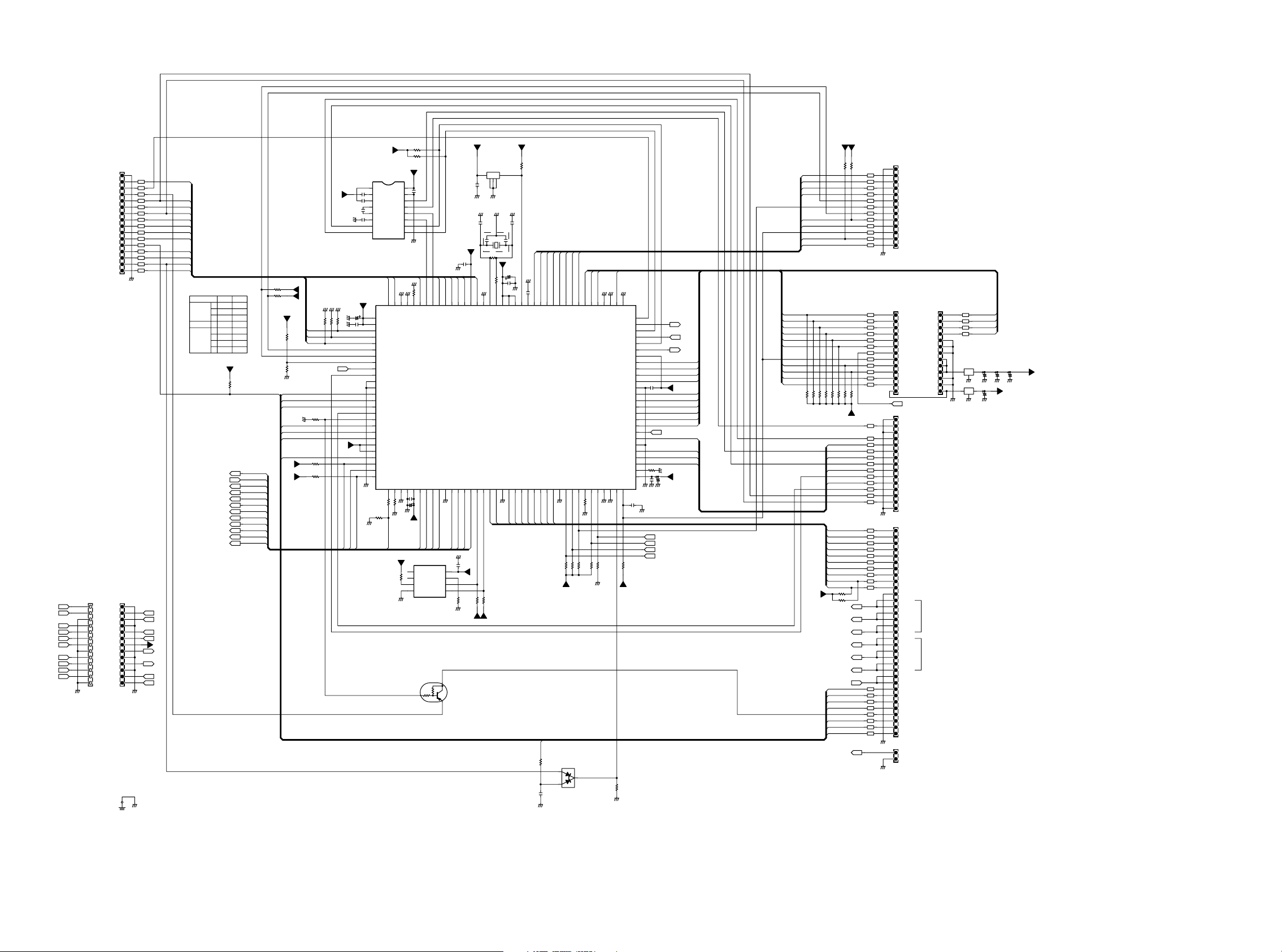
P604-2/2
QU04
123
GND
86
85
EXTAL
TU SD
GND
XU01
20MHz
3
21
Dummy
+5VL
0
0 1
RU17
CU06
84
83
VCC
XTAL
QU01
H8/2398
GNDGND
TU_ST
GND
GND
82NM81
_STBY
TU_MUTE
*p
CU08
_CE_TU
+5VL
RU14
Dummy
HEAT
HP ON
HP DET
FLRB ON
FLRA_ON
SURR ON
HEAT DET
_STANDBY
22u 6.3
GND
CU07
0.47
CU22
80
79
78
77
76
75
HP_ON
TUDOUT
GND
_HP_DET
TUCLK
RC IN
RU47
CU21
10p
_STANDBY
_HEAT_DET
GND
TUD N
RDSDIN
0
74
HEAT
+5VL +5VL
31
VCL
_RST
KILL RDS
_CERDS
CE VOLB
SURR_ON73FLRB_ON72FLRA_ON71CE_VOLB70CE_VOLA
22k
RU08
GND
47k
47k
47k
47k
RU05
RU06
RU09
RU07
DU01
2
CE_VOLA
69
47k
RU10
GND
VOLCLK
68
VOLCLK
VOLDATA
GND
GNDGND
GNDGND
66
65
VSS67VSS
VSS
64
CEFL
VOLDATA
63
DSPCLK
62
RXD
61
DSPDIN
60
TXD
59
DSPDOU
58
VCC
57
LRMUTE
56
SLSRMUTE
55
SBMUTE
54
CNTMUTE
53
VSS
52
SWMUTE
51
MULTIMUTE
50
CE TCB
49
CE TCA
48
AFCLK
47
AFDATA
46
H NBUSY
45
CE OSD
44
VSS
43
BP CVBS
42
BP Y
41
CE EXTA
40
NC
39
VCC
CU03
0 1
CU23
0 1
GND
GND
GND
47k
RU11
RU48
47k
GND
DSPCLK
DSPDIN
DSPDOUT
LRMUTE
SLSRMUTE
SBMUTE
CNTMUTE
+5VL
CU05
RU28
47k
GND
GND
RERR
REQ1
REQ2
0 1
CU04
22u/6 3
DIR INT
HINBUSY
GND
MULTIMUTE
+5VL
SWMUTE
CE TCB
CE TCA
AFCLK
AFDATA
CE OSD
BP CVBS
CE EXTA
BP Y
LRMUTE
SLSRMUTE
SBMUTE
CNTMUTE
SWMUTE
MULTIMUTE
CE TCB
CE TCA
AFCLK
AFDATA
FLRA ON
FLRB ON
SURR ON
HEAT
HEAT DET
STANDBY
HP DET
HP ON
47k
RU42
47k
RU41
+5VL+5VL
47k
47k
RU33
RU34
47k
47k
47k
47k
47k
47k
RU35
RU36
RU37
RU38
RU39
RU40
+5VL
CE EXTA
BP Y
BP CVBS
CE OSD
RDSDN
TUD N
TUCLK
TUDOUT
CERDS
KILL RDS
CE TU
TU MUTE
TU ST
TU SD
22k
RU43
+5VL
22k
RU44
SPDIFI[6]
SPDIFI[5]
SPDIFI[4]
SPDIFI[3]
SPDIFI[2]
SPDIFI[0]
SPD FO
WRITE
DC OUT1
DC OUT2
RC N
RC OUT
M RC IN
M RC OUT
SPDIFI[1]
LU35
LU36
LU37
LU38
LU39
LU40
LU41
LU42
LU43
LU77
LU78
LU44
GND
LU02
LU03
LU04
LU05
LU06
LU07
LU08
LU09
LU10
LU11
LU12
LU13
LU46
LU48
LU47
LU50
LU49
LU52
LU51
LU54
LU53
LU56
LU55
LU57
GND
LU58
LU59
LU60
LU61
LU62
LU63
LU64
LU65
LU66
LU67
LU69
LU70
LU71
LU72
1k
LU73
LU74
LU75
LU76
GND
GND
13
GND
12
FLRA ON
11
FLRB ON
10
SURR ON
9
HEAT
8
5V DOWN(NC)
7
P AMP FAIL
6
P LINE FAIL
5
HEAT DET
4
STANDBY
3
P DOWN
2
HP DET
1
HP ON
JU04
JU02 JU02
14
LRMUTE
CE VOLB
15
SLSRMUTE
CE VOLA
16
SBMUTE
JU05
JU07
CNTMUTE
SWMUTE
MULTIMUTE
ERMUTE
PDOWN
CE TCB
CE TCA
AFCLK
AFDATA
+5VL
ERMUTE
GND
CTS
GND
RXD
CE EXTA
RTS
BP Y
TXD
BP CVBS
TV AUTO
CE OSD
VSYNC
OSDCLK
OSDDATA
GND
RDSDIN
TUDIN
TUCLK
TUDOUT
CERDS
KILL RDS
CE TU
TU MUTE
TU ST
TU SD
GND
D G6 N
D G6 N
D G5 N
D G5 N
D G4 N
D G4 N
D G3 N
D G3 N
D G2 N
D G2 N
D G1 N
D G1 N
D GOUT
D GOUT
WRITE
DC OUT1
DC OUT2
RC IN
R
RCOUT
M RC IN
M RC OUT
33FMN
AUXIN
VOLCLK
VOLDATA
GND
GND
GND
+5VD
+5VD
+5VD
GND
GND
+5VL
COAX INPUT
OPT NPUT
17
18
19
20
21
22
23
24
25
26
15
14
13
12
11
10
9
8
7
6
5
4
3
2
1
33
32
31
30
29
28
27
26
25
24
23
22
21
20
19
18
17
16
15
14
13
12
11
10
9
8
7
6
5
4
3
2
1
JU06
1
2
1
2
3
4
5
6
7
8
9
10
11
12
13
GND GND
LU14
CE VOLB
LU15
CE VOLA
LU16
VOLCLK
LU17
VOLDATA
CU80
CU82 CU83
LU18
220/10
220/10 220 10
21
3
GND GND
GND
GND
LU19
21
3
GND
CU81
100/10
+5VD
+5VL
VOL-
VOL+93VOL-
GND
WP
2
1
+5VL
S 80145ALMC JA6 T2
54
0 1
CU20
GND
GND
*p
CU09
+5VL
RU18
0 1
CU11
GND
SEL-
RSFL
SEL+
GND
STBYLED
92
91
90
89
88
87
VCC
VSS
SEL+
SEL-
_RSFL
_STBYLED
XMODE
_CEDIR
D A
XSTATE
GND
CU19
0 1
8
+5VL
7
6
5
47k
47k
47k
RU45
RU04
RU03
GND
+5VL
+5VL
47k
RU19
+5VL
47k
RU20
JU03
1
GND
LU34
2
RSTFL
LU33
3
CEFL
LU32
4
RCOUT
LU31
5
OSDCLK
LU30
6
VOL+
LU29
7
OSDDATA
LU28
8
VOL
LU27
9
RSFL
LU26
10
STBYLED
LU25
11
KEY0
LU24
12
WRITE
LU23
13
KEY1
LU22
14
SEL+
LU21
15
KEY2
LU20
16
SEL
GND
JU01 JU01
1
SL
2
SL+
3
4
SR+
5
SR
SBL
SBL+
SBR+
SBR
CNT
CNT+
6
7
8
9
10
11
12
13
14
SL
GND
15
SL+
FR
16
GND
FR+
17
SR+
GND
18
SR
FL+
19
SBL
FL
20
SBL+
15V
21
GND
RT
22
SBR+
GND
23
SBR
LT
24
CNT
GND
25
CNT+
SW+
26
GND
SW
GNDGND
EARTH
JU10
GND
EARTH
RSTFL
OSDCLK
VOL+
OSDDATA
VOL
RSFL
STBYLED
KEY0
KEY1
SEL+
KEY2
SEL
47k
RU25
MODEL
RU26
RU27
0
USR7300/
39k
56k
K
22k
N
82k
56k
F
39k
PS7300/
27k
8 2k
K
N 82k
22k
F
100k
+5VL
RU49
47k
BTMOD
XSTATE
XMODE
CEDIR
D A
RSTADC
DFS
RSTDAC
RSTDSP
SCS
FCS
ATT
68k
82k
SR7300F U
FR
FR+
FL+
FL
-15V
RT
LT
SW+
SW
BTMOD
XSTATE
XMODE
CEDIR
RSTADC
RSTDAC
RSTDSP
47k
RU24
+5VD
+5VL
KEY0
KEY1
RU26
KEY2
RU27
GND
WRITE
M RC OUT
RC OUT
M RC IN
GND +5VL
DC OUT1
DC OUT2
RC IN
WRITE
+5VL+5VL
RU31
RU32
D A
DFS
SCS
FCS
ATT
GND
GND
4.7k
4.7k
RU22
RU23
OVFL
10k
RU30
47k
47k
RS 232C transm tters/receivers
QU03
ICL3232ECB
1
CU14
0 1
C1+
2
V+
+5VL
3
CU15
0 1
C1
4
C2+
0 1
CU16
5
C2
6
V
GND
CU17
0 1
7
T2out
8
R2in
+5VL
CU13
22u/6 3
GND
CU12
0 1
103
4.7k
GND
104
GND
RU21
105
106
107
108
109
110
111
112
113
114
115
116
117
118
119
120
121
122
123
+5VL
124
125
126
127
128
GND GND
RU50
10k
GND
SCS
FCS
_RSTDSP
+5VL
16
VCC
CU18
15
0 1
GND
14
T1out
13
R1in
12
R1out
11
T1n
10
T2n
9
R2out
GND
GND
RU12
10k
RSTFL
OSDCLK
102
101
100
VSS99VSS
_RSTFL
OSDCLK
AVCC
VREF
KEY0
KEY1
KEY2
5V DOWN
P LINE FAIL
MODE
OVFL
TV AUTO
AVSS
VSS
M RC OUT
RC OUT
M RC IN
VSYNC
KILLIR
DC OUT1
DC OUT2
RC IN
MD0
MD1
MD2
FCS
RSTDSP
SCS
BTMOD2NC3VSS4NC5VCC6_RSTDAC7DFS8_ATT9_RSTADC10VSS11D_A12XSTATE13_CEDIR14_XMODE15I CCLK16I CDATA17_TU_SD18TU_ST19VSS20TU_MUTE21_CE_TU22_KILL_RDS23_CERDS24TUDOUT25TUCLK26TUD N27RDSIN28VSS29REQ230DIR_INT31P_AMP_FAIL32IRQ733REQ134RERR35VSS36VSS37WAKEUP38_P_DOWN
1
22k
5.6k
RU02
RU01
GND
CU01
0 1
CU02
22u 6 3
BTMOD
+5VL
RU46
47k
GND
VOL+
OSDDATA
98SI97
96
94
RTS95CTS
OSDDATA
GND
+5VL
RSTDAC
RSTADC
DFS
_ATT
QU02
AT24C08
1
Vcc
A0
2
A1
3
SCL
A2
4
SDA
GND
QU06
RN2303
3
2423
Page 17
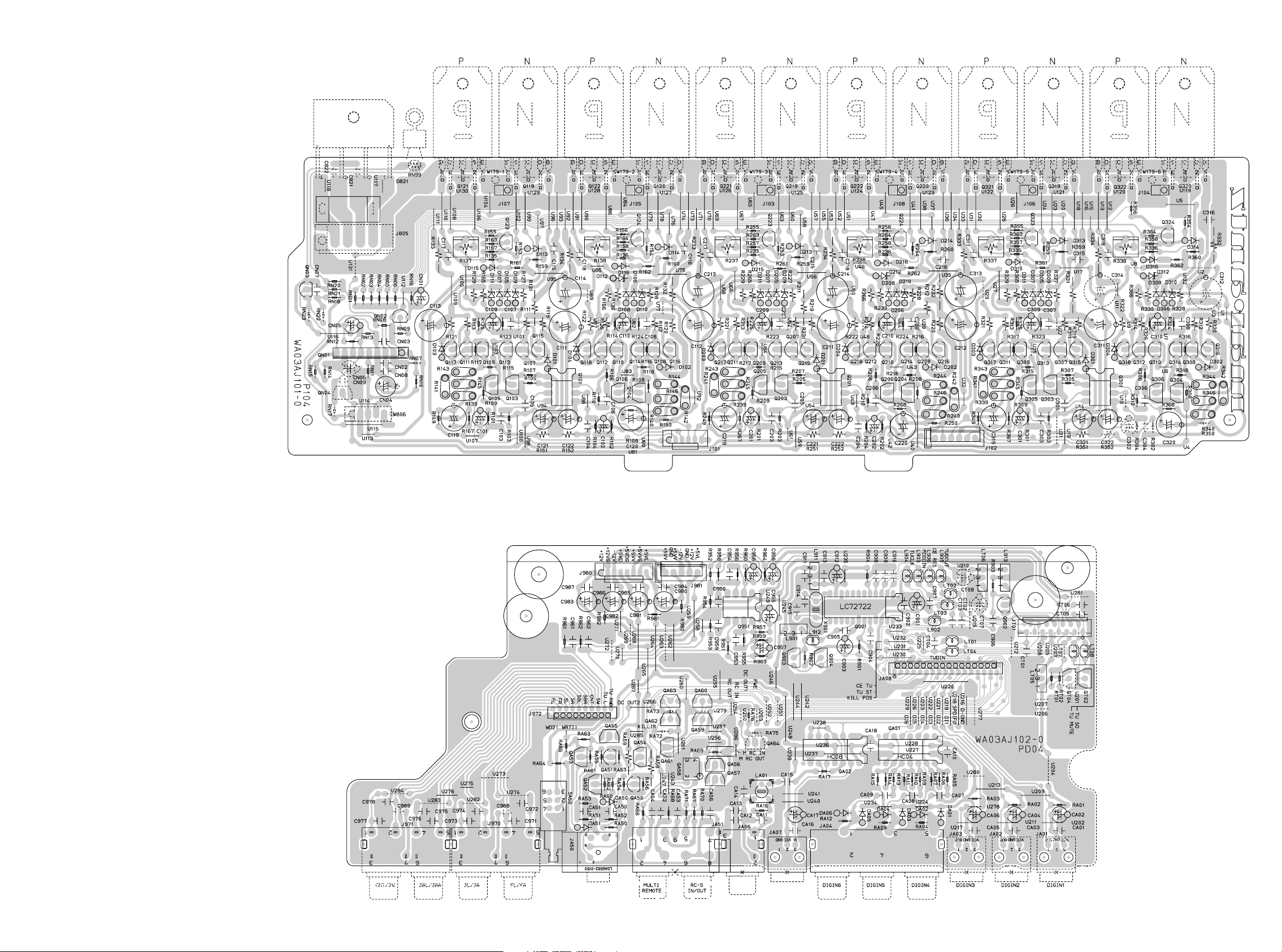
6. PARTS LOCATION
P104
QN03
QN04
QN02
Q121 Q119 Q122 Q120 Q221 Q219 Q222 Q220 Q321 Q319 Q322 Q320
Q123 Q124 Q223 Q224 Q223 Q324
Q117 Q111 Q109 Q113 Q107 Q115 Q118 Q112 Q110 Q114 Q108 Q116 Q217 Q211 Q209 Q213 Q207 Q215 Q218 Q212 Q210 Q214 Q208 Q216 Q317 Q311 Q309 Q313 Q307 Q315 Q318 Q312 Q310 Q314 Q308 Q316
Q105 Q103 Q101 Q106 Q104 Q205 Q203 Q201 Q206 Q204 Q305 Q303 Q301 Q306 Q304
PD04
Q951 Q903 Q904
QA50 - QA55 QA59 - QA63 QA56 QA57 QA64
Q901 QT04 QT02
QA02 QA01
25 26
Page 18
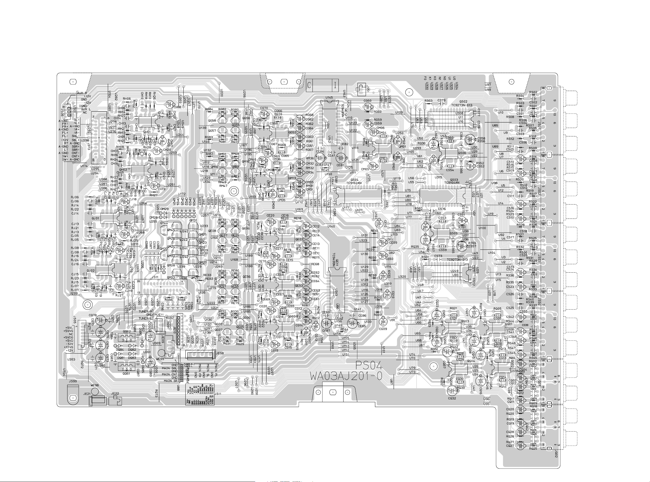
PS04
QJ01
QJ02
QH04
QG62 QG61
QH01
QM44 QM45
QM26 QM24
QM33 QM32
QM28 QM22
QM31 QM25
QM23 QM29
QM27 QM21
QG58 - QG55
QM18 - QM18
QE08 -QE05
QE58 - QE55
QG08 - QG05
QG53
QM13
QE03
QE53
QG03
QE11
QS04
QM01QE01 QS06
QS03
QS05
QS01
QQ03 QQ04 QQ01 QQ02
2827
Page 19
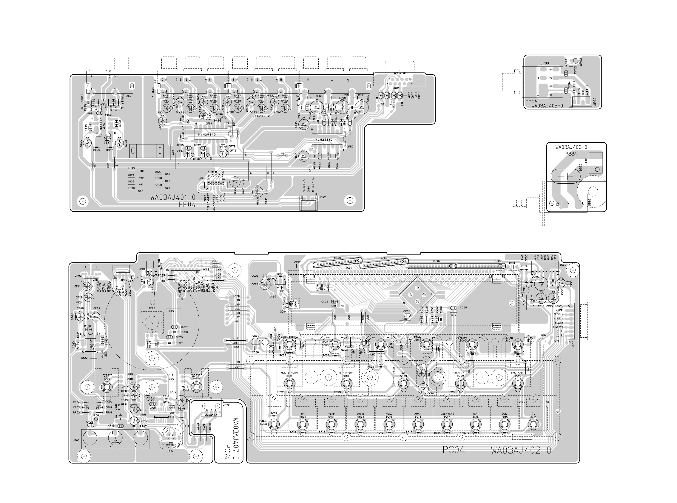
PF04
PP94
QS10 QF51 QF70
P884
PC04 PC74
PL01 QP02 QC03 QC05 QC02 QP01
29 30
Page 20

PL04
QL15 QL14 QL13 QL11 QL07 QL06
QL03QL08 QL09
QL10
QF03 QL05
QL12
QX05
QX03
QX04 QX01
QF01 QL81 QL80
QL01QL02
QL04
QF02
QX02
P804
Q803 Q804 Q801 Q802 QN60 - QN62 QN55 QN59
QN51 - QN54 QN56 - QN58
QP91 QP92
3231
Page 21

P854
Q854 Q852 Q823
PC64 PC54
QC51 QC50
P874
P864
P894
33
Page 22

P604 A
QR01
Q600
Q680 Q681 QU01 QU04
QD01
QK03 - QK05
34
Page 23

P604 B
QR02 QR04 QU02 QU06
QU03 Q603 Q601
QR03 QK03 QK02 QK01
35
Page 24

7. IC DATA
QU01 : H8S/2398F-ZTAT
Pin I/O Name
1 O BTMOD L FLASH ROM Address (A18)
2 I N.C - PULL DOWN
3 - VSS - GND
4 NC NC GND
5 I Vcc 6 O _RSTDAC L DAC
7 O DFS H DAC&I(AD)C
8O_ATT LADC
9 O _RSTADC L ADC
10 - VSS - GND
11 O D_A - DIR or _ADC sel
12 I XSTATE - DIR
13 O _CEDIR L DIR CHIP ENABLE
14 O _XMODE L DIR RESET
15 O IICCLK - I2C for E2PROM
16 I/O IICDATA - I2C for E2PROM
17 I _TU_SD L Tuned
18 I TU_ST H Stereo Tune/_MONO
19 - VSS - GND
20 O TU_MUTE H Tuner MUTE
21 O _CE_TU L Tuner Pack
22 O _KILL_RDS L Tuner Pack(RDS)
23 O _CERDS L Tuner Pack(RDS)
24 O TUDOUT - Tuner Pack
25 O TUCLK - Tuner Pack
26 I TUDIN - Tuner Pack
27 I RDSDIN - Tuner Pack(RDS)
28 - VSS - GND
29 I(INT) REQ2 L DSP FINTR EQ
30 I(INT) DIR_INT DIR INT OUTPUT
31 I(INT) _P_AMP_FAIL L Power amp Detect
32 I IRQ7 - PULL DOWN
33 I(INT) REQ1 L DSP INTER Q
34 I(INT) RERR H DIR ERROR
35 - VSS - GND
36 - VSS - GND
37 I(INT) WAKEUP
38 I(INT) _P_DOWN L Power Down Detect
39 I Vcc - +5V
40 O N.C - OPEN
41 O _CEEX L P-Exp(Video)Sel A
42 O Y_OSD H Y/C_OSD_IC_BYPASS
43 O CVBS_OSD H CVBS_OSD_IC_BYPASS
44 - VSS - GND
45 O _CEOSD L Video Circuit
46 I HINBSY - DSP Busy Signal
47 O AFDATA - Analog Switch DATA
48 O AFCLK - Analog Switch CLOCK
49 O CE_TCA H Analog Switch TC9273
50 O CE_TCB H Analog Switch TC9262/9264
51 O MULTIMUTE H MULTI ROOM MUTE
52 O SWMUTE H SUB W MUTE
53 - VSS - GND
54 O CNTMUTE H CENTER SP MUTE
55 O SBMUTE H SRR B MUTE
56 O SL/SRMUTE H SL SR MUTE
57 O L/RMUTE H FRONT L R MUTE
58 I Vcc - +5V
59 O(SO) DSPDOUT DSP DIR Control Data OUT
60 O(SO) TXD UART for Panja, Flash WR
61 I(SI) DSPDIN DSP DIR Control Data IN
62 I(SI) RXD UART for Panja, Flash WR
Port
Note
Act.
STANDBY MODE Release
↑
63 O(SC) DSPCLK DSP DIR Control CLOCK
64 O _CEFL L FL Driver chip sel
65 - VSS - GND
66 O VOLDATA - Volume IC DATA
67 - VSS - GND
68 - VSS - GND
69 O VOLCLK - Volume IC CLOCK
70 O CE_VOLA H Volume IC Chip Sel A
71 O CE_VOLB H Volume IC Chip Sel B
72 O FLRA_ON H SPK A SELECT
73 O FLRB_ON H SPK B SELECT
74 O SURR_ON H SURR/CNT/SB SPK ON
75 O HEAT H Power Amp ±B_L_Sel
76 I _HEAT_DET H
77 O _STANDBY L Standby Power
78 I _HP_DET L HP Jack Detect
79 O HP_ON H HEAD PHONE ON
80 - VCL 81 I _RST L Reset
82 NO NMI - Fix H
83 NO _STBY L Fix H
84 I Vcc - +5V
85 O XTAL - Xtal(20M)
86 I EXTAL - Xtal(20M)
87 - VSS - GND
88 I SEL- - Front Select. Encoder
89 I Vcc - +5V
90 I SEL+ - Front Select. Encoder
91 O _STBY LED L Standby LED On
92 O _RSFL L Front FL Driver
93 I VOL- - Front V ol. Encoder
94 I VOL+ - Front V ol. Encoder
95 I CTS - UART
96 O RTS UART
97 O(SO) OSDDATA - Front FL & Video(OSD)
98 I N.C - PULL DOWN
99 - VSS - GND
100 - VSS - GND
101 O(SC) OSDCLK - Front FL & Video(OSD)
102 O _RSTFL L Reset FL Driver
103 - AVCC - +5V
104 - VREF - +5V
105 I(AD) KEY0 - Front Key
106 I(AD) KEY1 - Front Key
107 I(AD) KEY2 - Front Key
108 I(AD) _5V_DOWN - Detect 5V
109 I(AD) P_LINE_FAIL - Emergency Protection
110 I(AD) MODE - CPU mode
111 I _OVFL H Peak Indicator
112 I(AD) TV_AUTO H TV Video Detect
113 - VSS - GND
114 - VSS - GND
115 O M_RC_OUT RC BUS MULTI OUTPUT
116 O RC_OUT RC BUS OUTPUT
117 I M_RC_IN L Multi RC5 IN Detect Signal
118 I VSYNC
119 O KILLIR H Kill to IR input signal.
120 O DC_OUT1 L DC T riger1
121 O DC_OUT2 L DC T riger2
122 I RC_IN
123 I MD0 - +5V
124 I MD1 - Fix H
125 I MD2 - Normal :H, Boot :L
126 O _FCS L DSP CHIP ENABLE
127 O _RSTDSP L DSP
128 O _SCS L DSP CHIP ENABLE
Power Amp Heat sink Temp
Detect
V-sync Det. & Change OSD
↑
IR In for RC-5
↑↓
36
Page 25

QK30 : CS5361-KSR
SCLK
VCOM LRCK
REFGND
V
L
SDOUT MCLK
RST
M/S
LRCK
SCLK
MCLK
VD
GND
VL
SDOUT
DIV
HPF
DIF
Pin Name
RST
M/S
LRCK
SCLK
MCLK
VD
GND
VL
SDOUT
DIV
124
223
322
421
520
619
718
817
916
10 15
11 14
12 13
I/O
I
I
I
I
I
I
I
I
O
I
Pin Description
#
Reset
(
1
2
3
4
5
6
7,18
8
9
10
Input
Master/Slave Mode
Left Right Clock
serial audio data line. The frequency of the left/right clock must be at the audio sample rate, Fs.
Serial Clock
Master Clock
several standard audio sample rates and the required master clock frequency.
Digital Power
ing Conditions for appropriate voltages.
Ground
(
Logic Power
ommended Operating Conditions for appropriate voltages.
Serial Audio Data Output
MCLK Divider
FILT+
REFGND
FILT+
Voltage R eference
VCOM
+
AINR
-
AINR
VA
GND
AINLAINL+
TST
M1
M0
) - The device enters a low power mode when low.
(
(
Input
(
Input
(
Input
) - Ground reference. Must be connected to analog ground.
Input
(
Input
(Input
AINL-
AINL+
AINR-
AINR+
-In Slave mode, LRCK and SCLK become input. (FIXED LOW)
(Input)
) - Determines which channel, Left or Right, is currently active on the
Input
) - Serial clock for the serial audio interface.
) - Clock source for the delta-sigma modulator and digital filters. Table 1 illustrates
)-Positive power supply for the digital section. Refer to the Recommended Operat-
)- Determines the required signal level for the digital input/output. Refer to the Rec-
(
Output
) - (FIXED LOW)
+
LP Filter
-
S/H
DAC
+
-
S/H
DAC
) - Output for two’s complement serial audio data.
Q
QLP Filter
Se rial Ou tpu t In ter fac e
Digital
Decimation
Filter
Digital
Decimation
Filter
High
Pass
Filt e r
High
Pass
Filt e r
RST
DIF
M/S
HPF
DIV
MODE0
MODE1
HPF
DIF
M0
M1
TST
AINL+
AINL-
VA
AINR+
AINR-
VCOM
REF_GND
FILT+
I
I
I
I
I
I
I
I
I
I
O
I
O
the indeterminate DC offsets introduced by the analog buffer stage and the analog modulator. The firstorder high pass filter response characteristics are detailed i n th e Digital Filter specifications table. The filter response scales linearly with sample rate.
Digital Interface Format
12
and serial data is defined by the Digital Interface Format selection. Refer to Figures 8 and 9.
Mode Selection
13,
14
(FIXED LOW)
Test Pin
15
Differential Left Channel Analog Input
16,
modulators via the AINL+/- pins. The full scale differential analog input level is specified in the Analog
17
Characteristics Specification table.
Analog Power
19
ating Conditions for appropriate voltages.
Differential Right Channel Analog Input
20,
modulators via the AINR+/- pins. The full scale differential analog input level is specified in the Analog
21
Characteristics Specification table.
Common Mode Voltage
22
the common mode voltage of the CS5361. VCOM is not buffered and the maximum current is 10 uA.
Reference Ground
23
to analog ground.
Positive Voltage Reference
24
Requires the capacitive decoupling to GND as shown in the Typical Connection Diagram.
(Input)
(
) -(FIXED LOW)
Input
-
This pin needs to be connected to GND.
)-Positive power supply for the analog section. Refer to the Recommended Oper-
(
Input
(
Input
High Pass Filter Enable
11
) -
(Input
(
(Output)
The device includes a high pass filter after the decimator to remove
) - The required relationship between the Left/Right clock, serial clock
Input
) - Signals are presented differentially to the delta -sigma
(
Input
) -Signals are presented dif ferentially to the delta-sigma
(
Input
-
Nominally 2.5 volts; can be used to bias the analog input circuitry to
) - Ground reference for the internal sampling circuits and must be connected
-
)
(
Output
Positive reference voltage for the internal sampling circuits.
37
Page 26

Q600 : CS4900X
Compressed
Audio
Interface
Digital
Audio
Interface
DSP AB
PLL Clock
Manager
Frame
Shifter
Input
Buffer
RAM
Programmable
Multistandard
Audio Decoder
Parallel or Serial
Host Interface
Shared Memory
SAI 0
SAI 1
SAI 3
SAI 2
DSP C
32-Bit DSP
DSP
RAM
Debug Port
Serial
Audio
Interface
DSP
ROM
External Memory
Digital
Audio
Interface
Internal Bus
Parallel or Serial
Interface
DAO 0
DAO 1
GPIO and I/O
Controller
Host Interface
Pin
I/O Function Description
No.
1 I/O UHS0, GPIO18 Mode Select Bit 0, General Purpose I/O
2 I/O UHS1, GPIO19 Mode Select Bit 1, General Purpose I/O
3 INTREQ Control Port Interrupt Request
4 I FA1, FSCDIN Host Address Bit One or SPI Serial Control Data Input
5 I/O GPIO20 General Purpose I/O
6 I FA0, FSCCLK Host Parallel Address Bit Zero or Serial Control Port Clock
7 I/O FHS2,
FSCDIO,
FSCDOUT
8 I/O GPIO21 General Purpose I/O
9 FDAT7 DSP AB Bidirectional Data Bus
10 VDD6 2.5V Supply Voltage
11 VSS6 2.5V Ground
12 FHS0, FWR,
FDS
13 O FHS1, FRD,
FR/W
14 FDAT6 DSP AB Bidirectional Data Bus
15 I FCS Host Parallel Chip Select, Host Serial SPI Chip Select
16 O FINTREQ Control Port Interrupt Request
17 FDBCK Reserved
18 FDAT5 DSP AB Bidirectional Data Bus
19 FDAT4 DSP AB Bidirectional Data Bus
20 VDD7 2.5V Supply Voltage
21 VSS7 2.5V Ground
22 FDAT3 DSP AB Bidirectional Data Bus
23 FDBDA Reserved
24 FDAT2 DSP AB Bidirectional Data Bus
25 DBDA Debug Data
26 DBCK Debug Clock
27 FDAT1 DSP AB Bidirectional Data Bus
28 TEST Reserved
29 FDAT0 DSP AB Bidirectional Data Bus
30 I/O NV_WE,
GPIO16
31 I/O NV_OE,
GPIO15
32 I/O NV_CS,
GPIO14
33 SD_WE SDRAM Write Enable
34 SD_DATA0,
EXTD0
35 SD_DATA1,
EXTD1
36 SD_DATA2,
EXTD2
37 SD_DATA3,
EXTD3
38 SD_DATA4,
EXTD4
39 SD_DQM0 SDRAM Data Mask 2
40 SD_DATA5,
EXTD5
41 VSSSD4 3.3V SDRAM/SRAM/EPROM Interface Ground
42 VDDSD4 3.3V SDRAM/SRAM/EPROM Interface Supply
43 SD_DATA6,
EXTD6
44 SD_DATA7,
EXTD7
45 SD_DQM1 SDRAM Data Mask 1
46 SD_DATA15,
EXTA18
47 SD_DATA14,
EXTA17
48 NC5 No Connect
49 SD_DATA13,
EXTA16
50 VSSSD3 3.3V SDRAM/SRAM/EPROM Interface Ground
51 VDDSD3 3.3V SDRAM/SRAM/EPROM Interface Supply
52 SD_DATA12,
EXTA15
Mode Select Bit 2 or Serial Control Port Data Input and
Output, Parallel Port Type Select
Mode Select Bit 0 or Host Write Strobe or Host Data Strobe
Mode Select Bit 1 or Host Parallel Output Enable or Host
Parallel R/W
SRAM Write Enable, General Purpose I/O
SRAM Output Enable, General Purpose I/O
SRAM Chip Select, General Purpose I/O
SDRAM Data Bus, SRAM External Data Bus
SDRAM Data Bus, SRAM External Data Bus
SDRAM Data Bus, SRAM External Data Bus
SDRAM Data Bus, SRAM External Data Bus
SDRAM Data Bus, SRAM External Data Bus
SDRAM Data Bus, SRAM External Data Bus
SDRAM Data Bus, SRAM External Data Bus
SDRAM Data Bus, SRAM External Data Bus
SDRAM Data Bus, SRAM External Address Bus
SDRAM Data Bus, SRAM External Address Bus
SDRAM Data Bus, SRAM External Address Bus
SDRAM Data Bus, SRAM External Address Bus
53 SD_DATA11,
EXTA14
54 SD_DATA10,
EXTA13
55 SD_DATA9,
EXTA12
56 SD_DATA8,
EXTA11
57 VSSSD2 3.3V SDRAM/SRAM/EPROM Interface Ground
58 VDDSD2 3.3V SDRAM/SRAM/EPROM Interface Supply
59 O SD_CLK_OUT SDRAM Clock Output
60 SD_ADDR9,
EXTA9
61 I SD_CLK_IN SDRAM Re-timing Clock Input
62 SD_ADDR8,
EXTA8
63 SD_ADDR7,
EXTA7
64 SD_CLK_EN SDRAM Clock Enable
65 SD_ADDR6,
EXTA6
66 SD_ADDR5,
EXTA5
67 SD_ADDR4,
EXTA4
68 SD_CS SDRAM Chip Select
69 VSSSD1 3.3V SDRAM/SRAM/EPROM Interface Ground
70 VDDSD1 3.3V SDRAM/SRAM/EPROM Interface Supply
71 SD_BA,
EXTA19
72 SD_ADDR10,
EXTA10
73 SD_ADDR0,
EXTA0
74 SD_ADDR1,
EXTA1
75 SD_ADDR2,
EXTA2
76 SD_ADDR3,
EXTA3
77 SD_RAS SDRAM Row Address Strobe
78 SD_CAS SDRAM Column Address Strobe
79 I/O SDATAN3,
GPIO27
80 I/O SDATAN2,
GPIO26
81 I/O SDATAN1,
GPIO25
82 I/O SDATAN0,
GPIO24
83 NC4 No Connect
84 NC3 No Connect
85 I/O LRCLKN,
GPIO23
86 I/O SCLKN,
GPIO22
87 O LRCLK1 Audio Output Sample Rate Clock
88 NC2 No Connect
89 NC1 No Connect
90 VDD1 2.5V Supply Voltage
91 VSS1 2.5V Ground
92 I/O AUDATA7,
XMT958B,
GPIO31
93 I/O AUDATA6,
GPIO30
94 I/O AUDATA5,
GPIO29
95 I/O HDATA7,
GPIO7
96 I/O HDATA6,
GPIO6
97 I/O HDATA5,
GPIO5
98 O SCLK1 Audio Output Bit Clock
SDRAM Data Bus, SRAM External Address Bus
SDRAM Data Bus, SRAM External Address Bus
SDRAM Data Bus, SRAM External Address Bus
SDRAM Data Bus, SRAM External Address Bus
SDRAM Address Bus, SRAM External Address Bus
SDRAM Address Bus, SRAM External Address Bus
SDRAM Address Bus, SRAM External Address Bus
SDRAM Address Bus, SRAM External Address Bus
SDRAM Address Bus, SRAM External Address Bus
SDRAM Address Bus, SRAM External Address Bus
SDRAM Bank Address Select, SRAM External Address Bus
SDRAM Address Bus, SRAM External Address Bus
SDRAM Address Bus, SRAM External Address Bus
SDRAM Address Bus, SRAM External Address Bus
SDRAM Address Bus, SRAM External Address Bus
SDRAM Address Bus, SRAM External Address Bus
PCM Audio Input Data, General Purpose I/O
PCM Audio Input Data, General Purpose I/O
PCM Audio Input Data, General Purpose I/O
PCM Audio Input Data, General Purpose I/O
PCM Audio Input Sample Rate Clock, General Purpose I/O
PCM Audio Input Bit Clock, General Purpose I/O
Digital Audio Output 7, S/PDIF Transmitter, General Purpose
I/O
Digital Audio Output 6, General Purpose I/O
Digital Audio Output 5, General Purpose I/O
DSP C Bidirectional Data Bus, General Purpose I/O
DSP C Bidirectional Data Bus, General Purpose I/O
DSP C Bidirectional Data Bus, General Purpose I/O
38
Page 27

Q600 : CS494001-CQ
Q901 : LC72722
99 MCLK Audio Master Clock
100 VDD2 2.5V Supply Voltage
101 VSS2 2.5V Ground
102 I/O AUDATA4,
GPIO28
103 I/O HDATA4,
GPIO4
Digital Audio Output 4, General Purpose I/O
DSP C Bidirectional Data Bus, General Purpose I/O
104 O SCLK0 Audio Output Bit Clock
105 I/O HDATA3,
GPIO3
106 O AUDATA3,
XMT958A
DSP C Bidirectional Data Bus, General Purpose I/O
Digital Audio Output 3, S/PDIF Transmitter
107 O AUDATA2 Digital Audio Output 2
108 O LRCLK0 Audio Output Sample Rate Clock
109 O AUDATA1 Digital Audio Output 1
110 O AUDATA0 Digital Audio Output 0
111 I CMPCLK,
FSCLKN2
112 I/O HDATA2,
GPIO2
PCM Audio Input Bit Clock
DSP C Bidirectional Data Bus, General Purpose I/O
113 VSS3 2.5V Ground
114 VDD3 2.5V Supply Voltage
115 I/O HDATA1,
GPIO1
116 I/O HDATA0,
GPIO0
117 O CMPREQ,
FLRCLKN2
118 I CMPDAT,
FSDATAN2
DSP C Bidirectional Data Bus, General Purpose I/O
DSP C Bidirectional Data Bus, General Purpose I/O
Frame Clock Data Request Out
PCM Audio Data Input Number Two
119 I FLRCLKN1 PCM Audio Input Sample Rate Clock
120 I/O WR, DS,
GPIO10
121 I/O RD, R/W,
GPIO11
Host Write Strobe, Host Data Strobe, General Purpose I/O
Host Parallel Output Enable, Host Parallel R/W, General
Purpose I/O
122 PLLVSS PLL Ground Voltage
123 FILT2 Phase Locked Loop Filter
124 FILT1 Phase-Locked Loop Filter
125 PLLVDD PLL Supply Voltage
126 O CLKOUT,
XTALO
Crystal Oscillator Output
127 I CLKIN, XTALI External Clock Input/Crystal Oscillator Input
128 CLKSEL DSP Clock Select
129 I/O CS, GPIO9 Host Parallel Chip Select, General Purpose I/O
130 I/O A0, GPIO13 Host Parallel Address Bit 0, General Purpose I/O
131 I FSDATAN1 PCM Audio Data Input One
132 VDD4 2.5V Supply Voltage
133 VSS4 2.5V Ground
134 I FSCLKN1,
STCCLK2
PCM Audio Input Bit Clock
135 SCS Host Serial SPI Chip Select
136 I SCDIN SPI Serial Control Data Input
137 VSS5 2.5V Ground
138 VDD5 2.5V Supply Voltage
139 I/O A1, GPIO12 Host Address Bit 1, General Purpose I/O
140 I/O SCDOUT,
SCDIO
141 I/O HINBSY,
GPIO8
Serial Control Port Data Input and Output
Input Host Message Status, General Purpose I/O
142 SCCLK Serial Control Port Clock
143 I/O UHS2,
CS_OUT,
GPIO17
Mode Select Bit 2, External Serial Memory Chip Select,
General Purpose I/O
144 I RESET Master Reset Input
Pin Functions
Pin No. Pin name Function
1 VREF Reference voltage output (Vdda/2)
2 MPXIN Baseband (multiplexed) signal input
5 FLOUT Subcarrier output (filter output)
6 CIN Subcarrier input (comparator input)
3 Vdda Analog system power supply (+5 V)
4 Vssa Analog system ground
12 XOUT Crystal oscillator output (4.332/8.664 MHz)
13 XIN Crystal oscillator input (external reference signal input)
7 T1 Test input (This pin must always be connected to ground.)
8T2
9 T3 (RDCL) Test I/O (RDS clock output)
10 T4 (RDDA) Test I/O (RDS data output)
11 T5 (RSFT) Test I/O (soft-decision control data output)
T6 (ERROR/
16
57K/TP/BE1)
T7 (CORREC/
17
ARI-ID/TA/BE0)
18 SYNC Block synchronization detection output
19 RDS-ID RDS detection output
20 DO Data output
21 CL Clock input
22 DI Data input
23 CE Chip enable
24 SYR Synchronization and RAM address reset (active high)
14 Vddd Digital system power supply (+5 V)
15 Vssd Digital system ground
Note: * Normally function as an output pin. Used as an I/O pin in test mode,
which is not available to user applications.
I/O
Output
Input
Output
Input
—
—
Output
Input
Input
Test input (standby control)
Input
0: Normal operation, 1: Standby state (crystal oscillator stopped)
I/O*
I/O*
I/O*
Test I/O (error status output, regenerated carrier output,
I/O*
TP output, error block count output)
Test I/O (Error correction status output, SK detection output,
I/O*
TA output, error block count output)
I/O*
Output
Output
Input
Input
Input
Input
—
—
Serial data interface (CCB)
Q901 : LC72722
Pin Assignment
124V
REF
223MPXIN CE
322Vdda DI
421Vssa CL
520FLOUT DO
LC72722
619CIN
LC72722M
718T1 SYNC
LC72722PM
817T2 T7(CORREC/ARI-ID/TA/BEO)
916
3(RDCL) T6(ERROR/57K/TP/BE1)
4(RDDA) Vssd
10 15
11 14
5(RSFT) Vddd
12 13X
OUT
Top view
SYR
RDS-ID
X
IN
Block Diagram
V
CCB
REF
57 kHz
BPF
SMOOTHING
(SCF)
(24 BLOCK DATA)
MEMORY CONTROL
FILTER
RAM
CINFLOUT
+
–
V
REF
ERROR CORRECTION
(SOFT DECISION)
CLK(4.332 MHz)
OSC/DIVIDER
X
IN
(57 kHz)
X
OUT
PLL
SYNC/EC CONTROLLER
SYNC
DETECT-1
CLOCK
RECOVERY
(1187.5 Hz)
DATA
DECODER
DETECT-2
SYNC
Vddd
Vssd
RDS-ID
SYNC
SYR
+5V +5V
Vdda
REFERENCE
VOLTAGE
Vssa
MPXIN
ANTIALIASING
FILTER
DO
CL
DI
CE
T3 to T7
T1
T2
TEST
39
Page 28

QR01 : LC89057W VF4-E
EMPHA/UO32AUDIO
33
/VO
INT
35
CL40CE39DI
XMODE
38
41
LC89057W-VF4-E
1
RXOUT
RX0
RX1
RX2
RX3
RX4
RX5/VI
RX6/UI
TMCK/PIO0
TBCK/PIO1
TLRCK/PIO2
TDATA/PIO3
TXO/PIOEN
LPF
C bit , Ubit
2
3
4
5
8
9
10
13
44
45
46
47
48
Input
Selector
Modulation
or
Parallel Port
XIN
29
Demodulation
Lock detect
PLL
28
XOUT
&
Microcontroller
Clock
Selector
27 34
XMCK CKST
I/F
Selector
Data
1/N
37
36
21
24
16
17
20
22
23
DO
RERR
RDATA
SDIN
RMCK
RBCK
RLRCK
SBCK
SLRCK
XMODE
DGND
DVDD
TMCK/PIO0
TBCK/PIO1
TLRCK/PIO2
TDATA/PIO3
TXO/PIOEN
DO
CE
CL
37
38
DI
39
40
41
42
43
44
45
46
47
48
LC89057W
No. Port name I/O Description
1 RXOUT O Data Output
2 RX0 I Digital data Input (TTL)
3 RX1 I Digital data Input (Coaxial)
4 RX2 I Digital data Input (TTL)
5 RX3 I Digital data Input (TTL)
6 DGND Digital GND
7 DVDD Digital VDD
8 RX4 I Digital data Input (TTL)
9 RX5/VI I Digital data Input (TTL)
10 RX6/UI I Digital data Input (TTL)
11 DVDD Digital GND for PLL
12 DGND Digital VDD for PLL
13 LPF O Loop filter for PLL
14 AVDD Analog VDD for PLL
15 AGND Analog GND for PLL
16 RMCK O System clock Output for R (256fs, 512fs, XIN, VCO)
17 RBCK O/I Bit clock Output for R (64fs)
18 DGND Digital GND
19 DVDD Digital VDD
20 RLRCK O/I LR clock Input/Output for R
21 RDATA O Serial Audio data Input
22 SBCK O Bit clock Output for S (32fs, 64fs, 128fs)
23 SLRCK O LR clock Output for S (fs/2, fs, 2fs)
24 SDIN I Serial Audio data Input
25 DGND Digital GND
26 DVDD Digital VDD
27 XMCK O Oscillation amplifier
28 XOUT O XOUT
29 XIN I XIN or External clock Input (24.576MHz or 12.288MHz)
30 DVDD Digital VDD
31 DGND Digital GND
32 EMPHA/UO I/O Emphasis Information / U data Output / Set for chip address
33 AUDIO/VO I/O Detected non-PCM / V flag Output / Set for chip address
34 CKST I/O Clock timing Output / Switch to master or slave for demodulation
35 INT I/O Interrupt Output / Switch to Modulation or general-purpose I/O
36 RERR O Error Output (PLL lock, data error)
37 DO O IF, Read out data Output
38 DI I IF, Write data Input
39 CE I IF, Chip enable Input
40 CL I IF, Clock Input
41 XMODE I System reset Input
42 DGND Digital GND
43 DVDD Digital VDD
44 TMCK/PIO0 I/O 256fs system-clock Input for modulation / General-purpose I/O input/output
45 TBCK/PIO1 I/O 64fs bit-clock Input for modulation / General-purpose I/O input/output
46 TLRCK/PIO2 I/O Fs clock Input for modulation / General-purpose I/O input/output
47 TDATA/PIO3 I/O Serial audio data for modulation / General-purpose I/O input/output
48 TXO/PIOEN O/I Modulation data Output / General-purpose I/O enable input
/VO
XOUT
XIN
DVDD
DGND
EMPHA/UO
AUDIO
CKST
INT
RERR
3536 3334 3132 2930 2728 2526
LC89057W-VF4-E
RX0
*** *
RXOUT
RX1
RX2
RX3
DGND
DVDD
RX4
RX5/VI
**
XMCK
1110987654321
RX6/UI
DVDD
DVDD
DGND
12
DGND
24
23
22
21
20
19
18
17
16
15
14
13
SDIN
SLRCK
SBCK
RDATA
RLRCK
DVDD
DGND
RBCK
RMCK
AGND
AVDD
LPF
40
Page 29

QE11/QE12 : TC9499N QU03 : HIN202ECB
TOP VIEW
0.1 F
0.1 F
T1
T2
16
V
CC
15
GND
14
T1
OUT
13
R1
IN
12
R1
OUT
11
T1
IN
10
T2
IN
9
R2
OUT
T2
C1+
C1-
C2+
C2-
OUT
R2
V+
V-
1
2
3
4
5
6
7
8
IN
+5V
16
1
C1+
+
3
C1-
4
C2+
+
5
C2-
+5V
400k
11
IN
+5V
400k
10
IN
V
CC
+5V TO 10V
VOLTAGE INVERTER
+10V TO -10V
VOLTAGE INVERTER
T1
T2
V+
0.1 F
+
2
6
V-
0.1 F
+
14
7
T1
T2
OUT
OUT
R1
R2
OUT
OUT
R1
R2
5k
5k
1312
89
GND
15
QU03 : HIN202ECB
Pin Descriptions
PIN FUNCTION
V
CC
V+ Internally generated positive supply (+10V nominal).
V- Internally generated negative supply (-10V nominal).
GND Ground Lead. Connect to 0V.
C1+ External capacitor (+ terminal) is connected to this lead.
C1- External capacitor (- terminal) is connected to this lead.
C2+ External capacitor (+ terminal) is connected to this lead.
C2- External capacitor (- terminal) is connected to this lead.
T
IN
T
OUT
R
IN
R
OUT
EN Enable Input. This is an active low input which enables the receiver outputs. With EN = 5V, the outputs are placed in a high
SD,
NC No Connect. No connections are made to these leads.
Power Supply Input 5V 10%, (5V 5% HIN207E).
Transmitter Inputs. These leads accept TTL/CMOS levels. An internal 400kΩ pull-up resistor to VCCis connected to each lead.
Transmitter Outputs. These are RS-232 levels (nominally ±10V).
Receiver Inputs. These inputs accept RS-232 input lev els . An internal 5kΩ pull-do wn resistor to GND is connected to each input.
Receiver Outputs. These are TTL/CMOS levels.
impedance state.
SD Shutdown Input. With SD = 5V (HIN213E SD = 0V), the charge pump is disabled, the receiver outputs are in a high impedance
state (except R4 and R5 of HIN241E) and the transmitters are shut off.
R1
R2
IN
IN
41
Page 30

QD01 : CS438243QD01 : CS4382
42
Page 31

Page 32

QC01 : NJU3430FG1
OSC
OSC
RST
SI
CS
CLK
RS
1
2
RESET
Instruction
Decoder
8bits
Shift
Reg.
Timing
Gen.
CR
OSC.
V
DD
V
SS
FDP
V
State
Reg.
Display
Cont rol
Line
Address
Address
Read
Address
Counter
Selector
Counter
MK RAM
CG RAM
CG ROM
DD RA M
No. SYMBOL I/O F U N C T I O N
16x2bit
35x8bit
8,400bi t
16x8bit
Icon
Segment
Port
Timing
Driver
Driver
Driver
Dri ve r
MK1MK
S1S
35
P
1
T1T
16
2
57 VDD - Power Source : VDD=+3.0 to 5.5V
49 V SS - GND : VSS=0V
48 VFDP -
50 OSC1 I
51 OSC2 O
VFD Driving Power Sourse
DD-20V to V DD-45V
V
CR Oscillation Terminal
External R and C connect to these terminals.
(Target f
OSC=360kHz)
Serial Clock Input Terminal
54 CLK I
The serial data input synchronizing the rise edge of this
terminal.
Chip Select Terminal
53 CS I
When the CS terminal is "H" the serial data input is not
available.
55 SI I
Serial Data Input Terminal
The data input is MSB first.
Register Selection Signal Input Terminal
56 RS I
RS="0" : Instruction Register
RS="1" : Data Register
Reset Terminal RST="L" : Reset
52 RST I
-Each Address
-Each RAM Data
-Display Digits
-Contrast Control
H
: (00)
: Unfixed
: 16-digit
: 8/16 Dury
-All Display Off
-All Outputs are "L"
61 to 64,
1 to 31
1 to S 35 O
S
Segment Output Terminals (Internal Pull-down
Resistance)
32 to 47 T1 to T16 O Timing Output Terminals (Internal Pull-down Resistance)
60
59
58 P1 O
MK1
MK2
O Icon Output Terminals (Internal Pull-down Resistance)
Output Port Terminal
This terminal is suitable for LED.
44
Page 33

QL03 : LC74781
Pin Functions
Pin No. Symbol Function Description
1V
2 Xtal
3 Xtal
4 CTRL1 Crystal oscillator input switching
5 BLANK Blanking output sync signal when MOD0 is high.) Outputs the crystal oscillator clock during reset (when the
6 OSC
7 OSC
8 CHARA Character output external synchronization signal is present or not. Outputs a high level when the synchronization
9 CS Enable input
10 SCLK Clock input
11 SIN Data input Serial data input. A pull-up resistor is built in (hysteresis input).
12 V
13 CV
14 NC Must be either connected to ground or left open.
15 CV
16 V
17 SYN
18 SEP
19 SEP
20 SEP
21 CTRL2 NTSC/PAL-M switching input PAL-N formats. A low level selects NTSC after a reset. The microprocessor command NTSC,
22 CTRL3 SEP
23 RST Reset input System reset input. A pull-up resistor is built in (hysteresis input).
24 V
1 Ground Ground connection (digital system ground)
SS
IN
Crystal oscillator connection
OUT
Used to connect the crystal oscillator and capacitor used to generate the internal
synchronization signal, or to input an external clock (2fsc or 4fsc).
Switches between external clock input mode and crystal oscillator mode.
Low = crystal oscillator mode, high = external clock mode
Outputs the blank signal (the OR of the character and border signals). (Outputs a composite
RST pin is low), but can be set up to not output this signal by microprocessor command.
IN
LC oscillator connection
OUT
Connections for the coil and capacitor that form the oscillator that generates the character
output dot clock.
Outputs the character signal. (Functions as the external synchronization signal discrimination
signal output pin when MOD0 is high, and outputs the state of the judgment as to whether the
signal is present.) Outputs the dot clock (LC oscillator) during reset, but can be set up to not
output this signal by microprocessor command.
Serial data input enable input. Serial data input is enabled when low. A pull-up resistor is built in
(hysteresis input).
Serial data input clock input.
A pull-up resistor is built in (hysteresis input).
2 Power supply Composite video signal level adjustment power supply pin (analog system power supply).
DD
Video signal output Composite video signal output
OUT
Video signal input Composite video signal input
IN
1 Power supply Power supply (+5 V: digital system power supply)
DD
Video signal input for the built-in sync separator circuit (Used for either horizontal
Sync separator circuit input synchronization signal or composite sync signal input when the built-in sync separator circuit is
IN
Sync separator circuit bias voltage Built-in sync separator circuit bias voltage monitor pin
C
not used.)
Built-in sync separator circuit composite sync signal output. (When MOD1 is high, outputs a high
Composite sync signal output level during internal synchronization and a low level during external synchronization.) (Outputs
OUT
Vertical synchronization Inputs a vertical synchronization signal created by integrating the SEP
IN
signal input integrator must be attached at the SEP
the SYN
input signal when the internal sync separator circuit is not used.)
IN
pin. This pin must be tied to VDD1 if unused.
OUT
pin output signal. An
OUT
The setting indicated by this pin takes priority in switching between the NTSC, PAL, PAL-M and
PAL, PAL-M, or PAL-N setting is valid. High = PAL-M format.
input control
IN
1 Power supply (+5 V) Power supply (+5 V: digital system power supply)
DD
Controls whether or not the VSYNC signal is input to the SEP
high = VSYNC not input.
input. Low = VSYNC input,
IN
QN01: TA7317P
Equivalemt Circuit Diagram
45 46
Page 34

8. EXPLODED VIEW AND PARTS LIST
5126
3X10( M)
x8
5128
3X8( M)
x3
5110
3X8( M)
x4
5128
3X8( M)
055G
5129
3X8( M)
075G
011K
021K
031K
041K
P854
T854
NONLY
920Gx16
5126
3X8( M)
PS14
5127
3X8( M)
x2
5128
3X8( M)
x3
P874
(/F/K/N)
075G
P854
J871
5127
3X8( M)
915G (U ONLY)
Z011
5127
3X8( M)
x2
5127
3X8( M)
x4
W001 (U ONLY)
5126
3X8( M)
906G
x2
5127
3X8( M)
x28
002B
030B
N&K&F ONLY
035B
5128
3X8( M)
x2
5128
3X8( M)
x2
5128
3X6( U)
030B
001D
5128
3X6( M)
x2
P884
036B
5126
3X15( M)
L
E
R
041Bx 3
033B
5127
3X8( M)
x3
MARK MATERI AL / FINISH
(M)
STEEL/ COPPER
(U)
STEEL/ BL ACK
(U ONLY)
5128
3X8( M)
x2
PP9 4
M
M
R
Y
T
U
N
I
N
F
P
M
E
003B(OSE ONLY)
001B
SYMBOL STYLE
51 04
51 10
51 26
5127
51 28
52 04
035B
( 007B)
(U ONLY)
5128
3X8( M)
x2
PC84
5128
3X8( M)
012B
PC64
(U ONLY)
PC54
018B
013B
014B
VC01
(010B)
( 005B)
PARTS NAME
+F. H. M. SCREW
+B. H. M. SCREW
+B. H. TAP TITE SCREW W /WASHER
+B. H . TAP TITE SCREW( W/ )
+B. H. TAP TITE SCREW(B T YPE)
+H. H. TAPT.B OLTS WITH FL ANGE(S TI TE)
P804
PC74
PC04
5128
3X8( M)
004B
FRONT ASSY.
5128
3X10( M)
011L
013L
5110
3X6( M)
x2
009L
x13
020B(OSE ONLY)
020B
5204
4X8( M)
x4
PC04
5128
3X8( M)
x8
T001
P104
HEAT- SI NK ASSY.
001L
P864
P894
L012
5128
03AJ
3X6( M)
003G
5128
3X6( M)
x6
005Lx2
x2
5129
4X10( M)
x3
050Gx2
PL04
P604
032G
034G
PS7300F ONLY
060Gx2
5128
3X8( M)
x4
5128
3X8( M)
x2
5129
3X8( M)
PS04
5104
3X6( M)
901G
036G
5128
3X8( M)
x2
009G
001G
x4
AT0 1
SR7300 ONLY
PF0 4
030Gx2
012Gx2
Z003
PD04
5127
3X8( M)
x5
5128
3X8( M)
x2
4847
Page 35

SR7300FSR7300
PS7300
VERS.
POS.
COLOR
NO
001B /N1B 03AJ248010 FRONT AL PANEL (BLACK) 03AJ248010
001B /U1B FRONT AL PANEL STANDBY
001B /K1G
001B /U1G FRONT AL PANEL STANDBY
002B 185J251010 MARANTZ BADGE 185J251010
004B BLACK 03AJ105500 CHASSIS FRONT MOLD ASSY (BL) 03AJ105500
004B GOLD 03AJ105510 CHASSIS FRONT MOLD ASSY (GL) 03AJ105510
005B BLACK 03AJ105020 CHASSIS FRONT MOLD (BLACK) 03AJ105020
005B GOLD 03AJ105120 CHASSIS FRONT MOLD (GOLD) 03AJ105120
010B BLACK 03AJ270010 BUTTON FUNCTION (BLACK) 03AJ270010
010B GOLD 03AJ270110 BUTTON FUNCTION (GOLD) 03AJ270110
030B BLACK 03AJ154010 KNOB MASTER (BLACK) 03AJ154010
030B GOLD 03AJ154020 KNOB MASTER (GOLD) 03AJ154020
033B 312J355010 LENS STANDBY 312J355010
035B /N1B 02AK270040 BUTTON POWER SW (BLACK) 02AK270040
035B /K1G
035B /U1B BUTTON POWER SW (BLACK) 320J270040
035B /U1G BUTTON POWER SW (GOLD) 320J270240
009G 03AJ057110 LEG 03AJ057110
055G 03AJ101030 SUPPORT FOR PCB AC OUT 03AJ101030
906G 396B010030 SCREW FOR RS-232C+R/P 396B010030
915G /U BUSH FOR AC CORD 450H259010
009L 343J010010 SCREW FOR TR&DIODE 343J010010
AT01 /U TUNER MODULE TFCE1U118A AV01202280
AT01 /K/N AV01203030 TUNER MODULE TFCE1E113A AV01203030
W601 nsp JUMPER LEAD FMN15-FMN
W602 nsp JUMPER LEAD FMN33-FMN
WC01 nsp JUMPER LEAD FMN16-FMN
WC02 nsp JUMPER LEAD FMN13-FMN
WG04 nsp JUMPER LEAD FMN19P-
WG05 nsp JUMPER LEAD 15FE
WL01 nsp JUMPER LEAD FMN11-FMN
WP03 nsp JUMPER LEAD FMN7P-FMN
PACKING
001T /U USER GUIDE SR7300 U 03AJ851250
001T /N 03AJ851310 USER GUIDE SR7300 N 03AJ851310
001T /K USER GUIDE SR7300 K 03AJ851350
Z003 ZK03AJ0010 REMOTE CONTROLLER
NOT STANDARD
001D BLACK LID TOP COVER (BLACK) 03AJ257010
001D GOLD LID TOP COVER (GOLD) 03AJ257110
001S /K/N/U PACKING CASE SR7300 03AJ801010
002S CUSHION 03AJ809010
/N1G
/N1G
T001 /U MAINS TRANSF. AC120V 60Hz TS60515040
T001 /K/N TS60515050 MAINS TRANSF. AC230/220V TS60515050
W001 /U MAINS CORD UL/CSA
Z011 /N ZC01803080 MAINS CORD 2P 10A 250V
Z011 /K MAINS CORD CCEE 10A 250V ZC01803090
PART NO.
(FOR EUR)
03AJ248110 FRONT AL PANEL (GOLD) 03AJ248110
02AK270140 BUTTON POWER SW (GOLD) 02AK270140
DESCRIPTION
(BLACK)
(GOLD)
NON-INTEGRA
JU05(P604)JL05(PL04
JU06(P604)JA08(PD04)
JC03(PC04)JU03(P604)
JU04(P604)J810(P804)
FMNJE10(PS04)J972(PD04)
JT01(PD04)TUNER PACK
JL06(PL04)JF54(PF04)
JP03(PC04)JS06(PS04)
RC7300SR
CLASS2
SPARE PARTS
PART NO.
(MJI)
03AJ248020
03AJ248120
YC02000880
YU15110520
YU33170520
YU16160520
YU13440520
YU19220520
YU15150500
YU11110520
YU07160520
ZK03AJ0010
ZC01803080
VERS.
POS.
COLOR
NO
001B /N1B 03AJ248210 FRONT AL PANEL (BLACK) OSE 03AJ248210
001B /U1B FRONT AL PANEL STANDBY
001B /K1G
001B /U1G FRONT AL PANEL STANDBY
002B 185J251010 MARANTZ BADGE 185J251010
003B 255W251010 BADGE OSE 255W251010
004B BLACK 03AJ105500 CHASSIS FRONT MOLD ASSY (BL) 03AJ105500
004B GOLD 03AJ105510 CHASSIS FRONT MOLD ASSY (GL) 03AJ105510
005B BLACK 03AJ105020 CHASSIS FRONT MOLD (BLACK) 03AJ105020
005B GOLD 03AJ105120 CHASSIS FRONT MOLD (GOLD) 03AJ105120
007B 03AJ158010 WINDOW OSE 03AJ158010
010B BLACK 03AJ270010 BUTTON FUNCTION (BLACK) 03AJ270010
010B GOLD 03AJ270110 BUTTON FUNCTION (GOLD) 03AJ270110
030B BLACK 03AJ154010 KNOB MASTER (BLACK) 03AJ154010
030B GOLD 03AJ154020 KNOB MASTER (GOLD) 03AJ154020
033B 312J355010 LENS STANDBY 312J355010
035B /N1B 02AK270040 BUTTON POWER SW (BLACK) 02AK270040
035B /K1G
035B /U1B BUTTON POWER SW (BLACK) 320J270040
035B /U1G BUTTON POWER SW (GOLD) 320J270240
009G 03AJ057110 LEG 03AJ057110
055G 03AJ101030 SUPPORT FOR PCB AC OUT 03AJ101030
906G 396B010030 SCREW FOR RS-232C+R/P 396B010030
915G /U BUSH FOR AC CORD 450H259010
009L 343J010010 SCREW FOR TR&DIODE 343J010010
AT01 /U TUNER MODULE TFCE1U118A AV01202280
AT01 /K/N AV01203030 TUNER MODULE TFCE1E113A AV01203030
T001 /U MAINS TRANSF. AC120V 60Hz TS60515040
T001 /K/N TS60515050 MAINS TRANSF. AC230/220V TS60515050
W001 /U MAINS CORD UL/CSA
W601 nsp JUMPER LEAD FMN15-FMN
W602 nsp JUMPER LEAD FMN33-FMN
WC01 nsp JUMPER LEAD FMN16-FMN
WC02 nsp JUMPER LEAD FMN13-FMN
WG04 nsp JUMPER LEAD FMN19P-
WG05 nsp JUMPER LEAD 15FE
WL01 nsp JUMPER LEAD FMN11-FMN
WP03 nsp JUMPER LEAD FMN7P-FMN
PACKING
001T /U USER GUIDE SR7300 U 03AJ851250
001T /N 03AJ851310 USER GUIDE SR7300 N 03AJ851310
001T /K USER GUIDE SR7300 K 03AJ851350
Z003 ZK03AJ0010 ZK03AJ0010
Z011 /N ZC01803080 MAINS CORD 2P 10A 250V
Z011 /K MAINS CORD CCEE 10A 250V ZC01803090
NOT STANDARD
001D BLACK LID TOP COVER (BLACK) 03AJ257010
001D GOLD LID TOP COVER (GOLD) 03AJ257110
001S /K/N/U PACKING CASE SR7300F 03AJ801030
002S CUSHION 03AJ809010
PART NO.
(FOR EUR)
03AJ248310 FRONT AL PANEL (GOLD) OSE 03AJ248310
/N1G
02AK270140 BUTTON POWER SW (GOLD) 02AK270140
/N1G
DESCRIPTION
(BLACK) OSE
(GOLD) OSE
NON-INTEGRA
JU05(P604)JL05(PL04
JU06(P604)JA08(PD04)
JC03(PC04)JU03(P604)
JU04(P604)J810(P804)
FMNJE10(PS04)J972(PD04)
JT01(PD04)TUNER PACK
JL06(PL04)JF54(PF04)
JP03(PC04)JS06(PS04)
CONTROLLER
REMOTE
CLASS2
SPARE PARTS
RC7300SR
PART NO.
(MJI)
03AJ248220
03AJ248320
YC02000880
YU15110520
YU33170520
YU16160520
YU13440520
YU19220520
YU15150500
YU11110520
YU07160520
ZC01803080
VERS.
POS.
COLOR
NO
001B BLACK FRONT AL PANEL (BLACK) 03AJ248040
001B GOLD FRONT AL PANEL (GOLD) 03AJ248140
002B MARANTZ BADGE 185J251010
004B BLACK CHASSIS FRONT MOUD ASSY(BL) 03AJ105530
004B GOLD CHASSIS FRONT MOUD ASSY
005B BLACK CHASSIS FRONT MOLD (BLACK) 03AJ105020
005B GOLD CHASSIS FRONT MOLD (GOLD) 03AJ105120
007B WINDOW (PS) 03AJ158040
010B BLACK BUTTON FUNCTION (BLACK) 03AJ270010
010B GOLD BUTTON FUNCTION (GOLD) 03AJ270110
030B BLACK KNOB MASTER (BLACK) 03AJ154010
030B GOLD KNOB MASTER (GOLD) 03AJ154020
033B LENS STANDBY 312J355010
035B BLACK BUTTON POWER SW (BLACK) 02AK270040
035B GOLD BUTTON POWER SW (GOLD) 02AK270140
009G LEG 03AJ057110
055G SUPPORT FOR PCB AC OUT 03AJ101030
906G SCREW FOR RS-232C+R/P 396B010030
009L SCREW FOR TR&DIODE 343J010010
T001 MAINS TRANSF. AC100V 50/60Hz TS60515060
W601 JUMPER LEAD FMN15-FMN
W602 JUMPER LEAD FMN33-FMN
WC01 JUMPER LEAD FMN16-FMN
WC02 JUMPER LEAD FMN13-FMN
WG04 JUMPER LEAD FMN19P-
WL01 JUMPER LEAD FMN11-FMN
WP03 JUMPER LEAD FMN7P-FMN
PACKING
001T USER GUIDE SR7300 F 03AJ851110
Z003 REMOTE CONTROLLER
Z011 MAINS CORD 2P
NOT STANDARD
001D BLACK LID TOP COVER (BLACK) 03AJ257010
001D GOLD LID TOP COVER (GOLD) 03AJ257110
001S PACKING CASE PS7300 03AJ801020
002S CUSHION 03AJ 809010
PART NO.
(FOR EUR)
DESCRIPTION
(GL)
JU05(P604)JL05(PL04
JU06(P604)JA08(PD04)
JC03(PC04)JU03(P604)
JU04(P604)J810(P804)
FMNJE10(PS04)J972(PD04)
JL06(PL04)JF54(PF04)
JP03(PC04)JS06(PS04)
RC7300SR
FOR 12A 125V AC
SPARE PARTS
PART NO.
(MJI)
03AJ105540
YU15110520
YU33170520
YU16160520
YU13440520
YU19220520
YU11110520
YU07160520
ZK03AJ0010
ZC01801050
NOTE : "nsp" PART IS LISTED FOR REFERENCE ONLY, MARANTZ WILL NOT SUPPLY THESE PARTS.
NOTE : "nsp" PART IS LISTED FOR REFERENCE ONLY, MARANTZ WILL NOT SUPPLY THESE PARTS.
49 50
Page 36

9. SERVICE PROGRAM
Factory Mode
With the following procedure, the Tracking Point, which is necessary for the adjustment and measurement of the tuner, can
be memorized.
1. Turn on the unit, press DVD, TUNER and 7.1ch - IN key simultaneously more than three seconds.
2. "FACTORY MODE" will be displayed on the FLD for two seconds and the following frequencies will be stored in the
Preset Memory.
Band Version P1 P2 P3 P4
FM AUTO
[MHz]
Band Scan Step P5 P6 P7 P8 P9 P10 P11 P12 P13
AM
[kHz]
9kHz(/F/N/K/S) 603 999 1404 531
Microprocessor (CPU), DSP Version and FLD Segment Check Mode
Turn the unit into the Factory Mode (See above) fi rst. Each time V-OFF button on the Remote controller is pressed or RC-5
code 161302 (Display) is entered, information shown on the FLD changes in the following order. Software versions of µ-com
and DSP can be seen and FLD segments can be checked.
/U /K/ S /N 90.0 98.0 106.0 87.5
/F 78.0 83.0 88.0 76.0
10 kHz (U) 600 1000 1400 520
No
Preset
Note : Step4, 5 is to check if CPU software is capable of DSP code. "Software Type No" is to show what "DSP Code Group"
CPU is capable of. And vice versa.
Step 8 is to manage the 16 codes for DSP.
• When the unit is once turned into Factory Mode, the unit keeps this mode until the main power is turned off.
(Turning into stand-by mode does not make it quit from Factory Mode.) When the unit quits from Factory Mode,
Information in the memory is also cleared and the unit returns to the status when it is out from the factory.
Product Reset
To reset the back up memory of the unit into the default status, follow the procedure below.
1. Turn of the unit and press SELECT and ATT keys simultaneously more than 1.5 seconds.
2. After "DEFAULT" is displayed on FLD, power is turned off once and turned of again, EEPROM is cleared to the default
status, µ-com is reset and the unit returns to the normal status. (Software Serial Number will not be cleared.)
Note : When the unit is shipped from the factory, the procedure above must be done to set the unit to initial status after the
tests.
1.Model Name is displayed.(Ex. : SR7300)
2.Software version of QU01(CPU) is displayed in the following format.
V020
Year Month Date
27 0
9
Ver.
3.Software Serial Number that is written in the factory is displayed.
MZXXXXXXXXXXX
4. Software Type Number is displayed
SOF T TYPE XX
(XX is displayed in Hex)
5. Group Type Number of the code that is written in the DSP’s external ROM is displayed.
CODE TYPEXXXX
6. 1G and 2G of the FLD is lighted each other. (Character part of Dot Matrix stays off.)
7. Dot Matrix part of the FLD lights in the checker pattern. (Other part stays off.)
8. Code ID of the code that is written in the DSP’s external ROM is displayed.
CDXX XXXXXXXX
Code No.
Device Code Sig Code T ype Version
ID ID ID
9. Returns to the step 1 and repeats the sequence.
10 . Press DISPLAY button to quit this mode.
5251
Page 37

10. UPDATE FIRMWARE
Software for CPU and DSP can be updated.
Have *SR7300CDR update disc.
There are two mode of download, regarding to the target of software as bellow.
Mode 1: Download DSP's software to 4M Flash-ROM.
This mode is to update the software for DSP.
The target devise is 4M Flash-ROM (Q601) on P604.
SR7300 need to be set download condition, by three front keys.
Mode 2: Download CPU's software to internal Flash-ROM.
This mode is to update the software for DSP.
The target devise is internal fl ash ROM of CPU (QU01) on P604.
The unit needs to be set to writing condition, by pushing internal switch from back-panel.
The following items are required for updating.
RS232C Dsub-9 pin cable (female to female/Straight type)
PC (Windows 98, NT, ME, 2000) with RS-232C port.
Upgrade software to CPU.
Upgrade software to DSP.
Use RS232C Dsub-9 pin cable (female to female/Straight type) to connect PC and the unit.
COM port on PC needs to be set by dialog box for each program. COM port can be set from COM1 to COM5.
Download Firmware for DSP (Mode 1)
1. Put the "DSP upgrade" folder into anywhere on your PC's hard disc.
2. Connect PC and the unit with the RS-232C cable.
3. Turn on the unit.
4. Press ENTER, MUTE and CD buttons simultaneously more than 5 seconds to turn the unit into Loading Mode.
5. "LOADING MODE" will be shown on FLD.
6. Launch "UpgradeDSP.exe" on PC.
7. Set the Baud Rate to 38400 then click Start communication button. If the connection is made successfully, a dialog box
saying "Success to connect" appears and "CONNECTED" is displayed on FLD.
8. Click Send the DSP codes button on the dialog box. Progress status of downloading will be shown on PC and OADING
is displayed on FLD.
9. If downloading is completed successfully, "COMPLETED" is displayed on FLD. And a dialog box saying "Finished the
DSP code transmitting" appears. Click OK and then click CLOSE to close the application.
10. Turn off the unit.
Download Firmware for CPU (Mode 2)
1. Put the "CPU upgrade" folder into anywhere on your PC's hard disc.
2. Connect PC and the unit with the RS-232C cable.
3. Insert a thin rot to the hole and push the switch (SA50) inside to turn on the switch.
53
Page 38

4. Turn on the power of the unit. (Confi rm that the stand-by LED lights in green so the unit is in the boot mode.)
5. Launch "H8Download.exe" on PC.
6. Click other fi les... button in the dialog box to specify the fi le (XXXX.mot) to be upload.
7. Click Connect button. If the connection with the H8
µ-com is successfully made, a dialogue box saying "Success to the
H8 micro processor connection" appears. If the connection fails, error message will appear.
8. Click Send button to start update.
9. If the fi rmware is updated successfully, a dialog box saying "Finished the fi rmware program sending" appears.
10. Click CLOSE button to close the application.
11. Disconnect Mains power cord.
12. Turn off the internal switch that has been turned on at step 3.
13. Turn on the unit.
Firmware Version Check
To check the versions of the fi rmware, see "Microprocessor (CPU), DSP Version and FLD Segment Check Mode" in
"SERVICE PROGRAM" section.
54
Page 39

11. POWER AMPLIFIER ADJUSTMENT
Idling Current Alignment
1. Each of the measurement points are provided with the two test points. Set a digital Voltage meter to DC voltage input,
connect the meter to the test points at both contact points.
2. After the setup above, turn on the main switch and heat up the amplifi er about 10 minutes.
3. Adjust variable resistors (R137, R138…R338) according to the digital voltmeter readings. The target setting value is 4.9
mV +/- 0.05 mV for each channels.
Settings : Master Volume --- Minimum
Speaker out --- No Load
Top lid --- OPEN
Channel
Front L R137 J107
Center R337 J106
Front R R273 J103
Surr. L R138 J105
Surr. R R238 J108
SB R338 J104
Time Table of Idling Current Rise
After Turning ON
5 min. 4.5 mV
10 min. 4.9 mV
20 min. 5.5 mV
30 min. 6.2 mV
40 min. 6.8 mV
60 min. 7.0 mV
Alignment
Point
Measurement
Point
Measurement Voltage
(R***)
55
Page 40

12. SYSTEM ERROR
The CPU inside the unit monitors peripheral interfaces and if a trouble is detected the following information is displayed on
the FLD.
1. Trouble in DSP
If communication with DSP is troubled more than 2 seconds, FLD shows below.
CHECK DSP
* This display stays and sound is muted.
2. Trouble in RS-232C
If communication with RS-232C of panja system is troubled more than 2 seconds, FLD shows below.
CHECK 232
3. Trouble in EEPROM
If data from EEPROM(QU70) does not match, FLD shows below.
CHECK E 2P
* After displaying it, Back-up Data is reset to default.
4. Trouble in EEPROM I/F
If communication with EEPROM(QU70) is troubled more than 2 seconds, FLD shows below.
CHECK E 2P I F
5. Trouble in 5V Supply
If 5V supply to P604(DSP/CPU PCB) is troubled, FLD shows below.
CHECK POW5
6. Trouble in Power Amplifi er
If DC offset, over-current, over-heat, trouble in main transformer is detected, FLD shows below.
C
PROTECT
* If a trouble is detected upon power on, CPU turns off the speaker relay. And if the trouble is not recovered within
2 seconds, CPU turns the unit into stand-by. If DC offset or over-current is detected on power on status, the
speaker relay is turned off, and if over-heat, trouble in main transformer is detected, the unit turns into stand-by
immediately.
56
Page 41

12. TROUBLE SHOOTING
No Power
Standby
LED Lights up in
standby mode
yes
FLD shows
PROTECT
?
yes
Supply +15V
to PU04?
yes
Supply +24V
to PU04?
yes
PU04 has any problem.
QU01(76p or 77p) lnput level
is too Low.
no
no
no
no
Power supply circuite (P854)
has any problem.
To be check +5VL or
_P_DOWN signal.
Vkk or FL is not supplied
to PC04
Can PY04
supply +15V ?
yes
Can PY04
supply +24V ?
yes
Connection has
problem
no
no
PB04 or Sub Transf (LB01)
has any problem
Relay
(LB02:PB04)
control is OK ?
yes
PY04,or Main Transf(L001)
has any problem
no
PB04 , or connection has
any problem
No picture
from Monitor output
no
VCR1&2 out
are OK ?
yes
Video Input select circutes
have problem
no
OSD menu is
shown?
OSD IC (QL03) or have
driver QL04, QX04 have
any trouble
yes
OSD ICs control is no problem
Video output stage are no problem
Input to OSD IC(QL03) has any trouble.
Video input detection has any trouble.
To be ckeck VSYNC or QL02
57
Page 42

No sound from SPK on
Analog Stereo mode
Pre output is
active ?
yes
P104
has problem
No sound
from SPK on PCM
STEREO(Digital In)
Pre output is
OK ?
no
Test Tone is
no
(Volume, & Power Amp are OK)
PS04(Audio In) orP604
(QK30:ADC)has any problem
OK ?
yes
no
Analog
S-Direct is
OK ?
(Volume , Power Amp &
Audio Input are OK)
QK30,Q600(P604)
has problem
no
yes
Volume(QE11)
has any problem.
yes
P104
has problem
Volume(QE11)
has any trouble.
DSP(Q600) input stage has any trouble.
To be check between QR01 and Q600
no
Analog
S-Direct are
OK ?
yes
Encode status
FLD shows ?
yes
Test tone is
OK ?
yes
no
DSP : Q600(P604)
DIR : QR01(P604)
has any trouble
DSP (Q600) or
no
DAC (QD01)
has any trouble
58
Page 43

No sound
from SPK on
AC-3/DTS decode
7.1ch Direct
is OK ?
yes
Volume(QE11)
no
Pre out has any trouble.
To be check PS04
P604 has trouble
Pre output is
OK ?
yes
P104
has problem
No sound
from SPK on
analog Dolby
no
Test tone is
OK ?
yes
DD,DTS,PCM
are shown?
yes
Error Mute circuite has trouble.
To be check QM44 or QR02
7.1ch Input
is OK ?
no
DAC & DSP are no problem
no DIR(QR01) or QR06
has any trouble.
to be check
signal(SDIDR)
Decoding is no problem
Volume(QE11)
no
Pre out has any trouble.
To be check PS04
DD,DTS,PCM
are shown?
yes
DIR & Q600 input is no problem
Q600 has trouble.
no
DIR(QR01)
has trouble
Pre output is
OK ?
yes
P104
has problem
yes
P604 has trouble
no no
Test tone is
OK ?
yes
DAC & DSP-out are no problem
Digital PCM
ProLogic is OK
?
yes
Decoding is no problem
ADC(QK30) has any trouble. Clock inputs from QK30 are
QD01 can not output data. any trouble
To be check QK30 or Lt/Rt
input on P604
no
DIR(QR01)
has any trouble.
To be check
signal(SDIDR)
59
Digital PCM
ProLogic is OK
?
yes
no
Q600 or DAC
has trouble
Q600 & DAC are no problem
Page 44

HOW TO FIND OUT DEFECTIVE POINT
AUDIO
Which signal path has problem Digital or Analog.
• Confi rm 6.1 / 7.1ch INPUT Mode.
• Confi rm S-Direct mode to analog input.
• Confi rm Test Tone output.
• Confi rm Multi Channel Stereo mode to analog input.
• Confi rm Multi Channel Stereo mode to PCM input.
VIDEO
Which stage has problem Input, Output or OSD?
• Confi rm VCR1 or VCR2 output.
• Confi rm both Monitor outputs (S-Video & CVBS) to normal condition.
• Confi rm Monitor output to system setup menu condition.
• Confi rm Monitor output to OSD information (Super imposes).
Video
input
R
VC
put
S-video
input
Component
input
CVBS
Sel.
Multi
CVBS
Sel.
Y
Sel.
C
Sel.
Comp
Sel.
Video Block Diagram
I/O Expander
Comp
Driver
SEL.
CPU
OSD
SEL. SEL.
SEL.
SEL.
Multi CVBS
Monitor
CVBS
Monitor
S-Video
Monitor
Component
60
Page 45

14. ELECTRICAL PARTS LIST
ASSIGNMENT OF COMMON PARTS CODES.
RESISTORS
R : 1) GD05 × × × 140, Carbon film fixed resistor, ±5% 1/4W
R : 2) GD05 × × × 160, Carbon film fixed resistor, ±5% 1/6W
Examples ;
Resistance value
➀
0.1 Ω.... 001 10 Ω .... 100 1 kΩ .... 102 100 kΩ.... 104
0.5 Ω.... 005 18 Ω .... 180 2.7 kΩ .... 272 680 kΩ.... 684
1 Ω .... 010 100 Ω .... 101 10 kΩ .... 103 1 MΩ.... 105
6.8 Ω.... 068 390 Ω .... 391 22 kΩ .... 223 4.7 MΩ .... 475
Note : Please distinguish 1/4W from 1/6W by the shape of parts
used actually.
CAPACITORS
C : CERAMIC CAP.
3) DD1 × × × × 370, Ceramic capacitor
Examples ;
Tolerance (Capacity deviation)
➁
±0.25 pF.... 0
Tolerance of COMMON PARTS handled here are as follows :
C : CERAMIC CAP.
Examples ;
C : 5) ELECTROLY CAP. ( ), 6) FILM CAP. ( )
Examples ;
0.5 pF 5 pF .... ±0.25 pF
Capacity value
➂
0.5 pF .... 005 3 pF ....030 100 pF .... 101
1.5 pF .... 015 47 pF .... 470 560 pF .... 561
4) DK16 × × × 300, High dielectric constant ceramic
Capacity value
➃
100 pF .... 101 1000 pF ....102 10000 pF .... 103
470 pF .... 471 2200 pF ....222
5) EA × × × × × × 10, Electrolytic capacitor
Capacity value
➄
0.1 µF....104 4.7 µF ....475 100 µF....107
0.33 µF....334 10 µF ....106 330 µF ....337
Working voltage
➅
{
➂
{
{
➅
Resistance value
Disc type
Temp.coeff.P350 N1000, 50V
Capacity value
Tolerance
capacitor
Disc type
Temp.chara. 2B4, 50V
Capacity value
One-way lead type, Tolerance ±20%
Working voltage
Capacity value
2200 µF....228
➀
{
➁
±0.5 pF.... 1
±5%.... 5
6 pF 10 pF ....±0.5 pF
12 pF 560 pF .... ±5%
1 pF .... 010 10 pF .... 100 220 pF ....221
➃
{
➄
1 µF ....105 22 µF ....22 6 1100 µF....11 8
6.3V....006 25V ....025
10V....01 0 35 V ....035
16V....01 6 50 V ....050
NOTE ON SAFETY FOR FUSIBLE RESISTOR :
The suppliers and their type numbers of fusible resistors
are as follows;
1. KOA Corporation
Part No. (MJI) Type No. (KOA) Description
NH05 × × × 140 RF25S × × × × ΩJ(±5% 1/4W)
NH05 × × × 120 RF50S × × × × ΩJ(±5% 1/2W)
NH85 × × × 110 RF73B2A × × × × ΩJ(±5% 1/10W)
NH95 × × × 140 RF73B2E × × × × ΩJ(±5% 1/4W)
2. Matsushita Electronic Components Co., Ltd
Part No. (MJI) Type No. (MEC) Description
NF05 × × × 140 ERD-2FCJ × × × (±5% 1/4W)
RF05 × × × 140
NF02 × × × 140
RF02 × × × 140
Examples ;
{
Resistance value
ERD-2FCG
{
Resistance value
Resistance value
0.1 Ω.... 001 10 Ω .... 100 1 kΩ .... 102 100 kΩ.... 104
0.5 Ω.... 005 18 Ω .... 180 2.7 kΩ .... 272 680 kΩ .... 684
1 Ω .... 010 100 Ω .... 101 10 kΩ .... 103 1 MΩ.... 105
6.8 Ω.... 068 390 Ω .... 391 22 kΩ .... 223 4.7 MΩ .... 475
{
Resistance value
(0.1 Ω − 10 kΩ)
× × × (±2% 1/4W)
{
Resistance value
ABBREVIATION AND MARKS
ANT. : ANTENNA BATT. : BATTERY
CAP. : CAPACITOR CER. : CERAMIC
CONN. : CONNECTING DIG. : DIGITAL
HP : HEADPHONE MIC. : MICROPHONE
µ-PRO : MICROPROCESSOR REC. : RECORDING
RES. : RESISTOR SPK : SPEAKER
SW : SWITCH TRANSF. : TRANSFORMER
TRIM. : TRIMMING TRS. : TRANSISTOR
VAR. : VARIABLE X’TAL : CRYSTAL
NOTE ON FUSE :
Regarding to all parts of parts code FS20xxx2xx, replace
only with Wickmann-Werke GmbH, Type 372 non glass type
fuse.
6) DF15 × × × 350 Plastic film capacitor
DF15 × × × 310 One-way type, Mylar ±5% 50V
DF16 × × × 310 Plastic film capacitor
Examples ;
Capacity value
➆
0.001 µF(1000 pF) ....... 102 0.1 µF....104
0.0018 µF........................ 182 0.56 µF....564
0.01 µF........................ 103 1 µF....105
0.015 µF........................ 153
: 1) The above CODES ( R , R , C , C and
NOTE
C ) are omitted on the schematic diagram in some
case.
2) On the occasion, be confirmed the common parts on
the parts list.
3) Refer to “Common Parts List” for the other common
parts (RI05, DD4, DK4).
➆
{
One-way type, Mylar ±10% 50V
Capacity value
NOTE ON SAFETY :
Symbol Fire or electrical shock hazard. Only original
parts should be used to replaced any part marked with
symbol . Any other component substitution (other
than original type), may increase risk of fire or electrical
shock hazard.
010728MIT
61
Page 46

SR7300/SR7300F
(VERS. COLOR : 7300·····SR7300 ALL VERSION. 7300F·····SR7300F(OSE) ALL VERSION.
VERS.
POS.
COLOR
NO
P104-6CHANNEL POWER
P104-CAPACITORS
C101 nsp ELECT. 10µF M 50V RA-2 OA10605020
C102 nsp ELECT. 10µF M 50V RA-2 OA10605020
C109 nsp ELECT. 22µF M 50V RA-2 OA22605020
C110
C111
nsp ELECT. 100µF 63V M RA-2 OA10706320
7300
C114
C119
C119 7300F nsp ELECT. 100µF M 50V RA-2 OA10705020
C120 7300 nsp ELECT. 100µF M 16V RA-2 OA10701620
C120 7300F nsp ELECT. 100µF M 50V RA-2 OA10705020
C121 nsp ELECT. 100µF M 16V RA-2 OA10701620
C122 nsp ELECT. 100µF M 16V RA-2 OA10701620
C201 nsp ELECT. 10µF M 50V RA-2 OA10605020
C202 nsp ELECT. 10µF M 50V RA-2 OA10605020
C209 nsp ELECT. 22µF M 50V RA-2 OA22605020
C210 nsp ELECT. 22µF M 50V RA-2 OA22605020
C211
C214
C219 7300 nsp ELECT. 100µF M 16V RA-2 OA10701620
C219 7300F nsp ELECT. 100µF M 50V RA-2 OA10705020
C220 7300 nsp ELECT. 100µF M 16V RA-2 OA10701620
C220 7300F nsp ELECT. 100µF M 50V RA-2 OA10705020
C221 nsp ELECT. 100µF M 16V RA-2 OA10701620
C222 nsp ELECT. 100µF M 16V RA-2 OA10701620
C301 nsp ELECT. 10µF M 50V RA-2 OA10605020
C302 nsp ELECT. 10µF M 50V RA-2 OA10605020
C309 nsp ELECT. 22µF M 50V RA-2 OA22605020
C310 nsp ELECT. 22µF M 50V RA-2 OA22605020
C311
C314
C319 7300 nsp ELECT. 100µF M 16V RA-2 OA10701620
C319 7300F nsp ELECT. 100µF M 50V RA-2 OA10705020
C320 7300 nsp ELECT. 100µF M 16V RA-2 OA10701620
C320 7300F nsp ELECT. 100µF M 50V RA-2 OA10705020
C321 nsp ELECT. 100µF M 16V RA-2 OA10701620
C322 nsp ELECT. 100µF M 16V RA-2 OA10701620
CN01 nsp ELECT. 4.7µF M 50V RA-2 OA47505020
CN04 nsp ELECT. 4.7µF M 50V RA-2 OA47605020
CN05 nsp ELECT. 0.47µF M 50V RA-2 OA47405020
P104 CAPACITORS (COMMON)
P104-RESISTORS
R137 RA02210760 TRIM. 220
R138 RA02210760 TRIM. 220
R139
R146
R237 RA02210760 TRIM. 220
R238 RA02210760 TRIM. 220
R239
R246
R337 RA02210760 TRIM. 220
R338 RA02210760 TRIM. 220
7300F
7300 nsp ELECT. 100µF M 16V RA-2 OA10701620
nsp ELECT. 100µF 63V M RA-2 OA10706320
7300
7300F
nsp ELECT. 100µF 63V M RA-2 OA10706320
7300
7300F
HIGH DIELECTRIC CONSTANT
PLASTIC FILM CAPACITOR
NK05470010 METAL ERG1SJ470E 1W NK05470010
NK05470010 METAL ERG1SJ470E 1W NK05470010
PART NO.
(FOR EUR)
nspnsp ELECT. 22µF M 50V RA-2 OA22605020
nsp
nsp
nsp
DESCRIPTION
AMPRIFIER CIRCUIT BOARD
ELECT. 220µF 63V M RA-2
ELECT. 220µF 63V M RA-2
ELECT. 220µF 63V M RA-2
CER. CAPACITOR ±10% 50V :
C103 C104 C107 C203 C204 C303
C304
±5% 50V : C107 C108 C207 C208
C307 C308
Ω
VERTI RA02210760
Ω
VERTI RA02210760
Ω
VERTI RA02210760
Ω
VERTI RA02210760
Ω
VERTI RA02210760
Ω
VERTI RA02210760
PART NO.
(MJI)
OA22706320
OA22706320
OA22706320
VERS.
POS.
COLOR
NO
R339
NK05470010 METAL ERG1SJ470E 1W NK05470010
R346
RN99 HP00029230 VARISTOR
P104-RESISTORS (COMMON)
P104-SEMICONDUCTORS
D101
D108 1SS176 MA165 1SS254 30V 0.1A
D109
D112
D113
D116 HSS81TD 150V 150MA AXIAL
D201
D208 1SS176 MA165 1SS254 30V 0.1A
D209
D212
D213
D216 HSS81TD 150V 150MA AXIAL
D301
D308 1SS176 MA165 1SS254 30V 0.1A
D309
D312
D313
nsp DIODE HD20027010
D316 HSS81TD 150V 150MA AXIAL
K101 HN000012A0 IC SAP17P SAP17N O AND Y HN000012A0
K102 HN000012A0 IC SAP17P SAP17N O AND Y HN000012A0
K201 HN000012A0 IC SAP17P SAP17N O AND Y HN000012A0
K202 HN000012A0 IC SAP17P SAP17N O AND Y HN000012A0
K301 HN000012A0 IC SAP17P SAP17N O AND Y HN000012A0
K302 HN000012A0 IC SAP17P SAP17N O AND Y HN000012A0
Q101 HC10053090 IC NJM-2068-DD HC10053090
Q103 HT110482B0 TRS. 2SA1048 Y OR GR HT110482B0
Q104 HT110482B0 TRS. 2SA1048 Y OR GR HT110482B0
Q105 HT324582B0 TRS. 2SC2458 Y OR GR HT324582B0
Q106 HT324582B0 TRS. 2SC2458 Y OR GR HT324582B0
Q107
Q110
Q111
Q114
Q115 HT111452A0 TRS. 2SA1145 O OR Y HT111452A0
Q116 HT111452A0 TRS. 2SA1145 O OR Y HT111452A0
Q117 HT327052A0 TRS. 2SC2705 O OR Y HT327052A0
Q118 HT327052A0 TRS. 2SC2705 O OR Y HT327052A0
CARBON FILM FIXED RES.
nsp DIODE HD20002000
HD30391000 ZENER DIODE 3.9V HD30391000
nsp DIODE HD20027010
nsp DIODE HD20002000
HD30391000 ZENER DIODE 3.9V HD30391000
nsp DIODE HD20027010
nsp DIODE HD20002000
HD30391000 ZENER DIODE 3.9V HD30391000
D821 HE20024290 DIODE D10XB SIP 10A HE20024290
HT109702A0 TRS. 2SA970 GR OR BL HT109702A0
HT322402A0 TRS. 2SC2240 GR OR BL HT322402A0
Q119 HC20002080 IC SAP17N O AND Y HC20002080
PART NO.
(FOR EUR)
DESCRIPTION
PTFM04BD222Q2N34B0 100C
±5% 1/6W : R101-R110 R115-R118
R123-R126 R135 R136 R149 R150
R153-R164 R167 R168 R201-210
R215-218 R223-R236 R249 R250
R253-R264 R267 R268 R301-R310
R315-R318 R323-R326 R349 R350
R353-R364 RR367 R368 RN01
RN02-RN23
PART NO.
(MJI)
HP00029230
NOTE : "nsp" PART IS LISTED FOR REFERENCE ONLY, MARANTZ WILL NOT SUPPLY THESE PARTS.
62
Page 47

SR7300/SR7300F
(VERS. COLOR : 7300·····SR7300 ALL VERSION. 7300F·····SR7300F(OSE) ALL VERSION.
VERS.
POS.
COLOR
NO
Q120 HC20002080 IC SAP17N O AND Y HC20002080
Q121 HC20001080 IC SAP17P O AND Y HC20001080
Q122 HC20001080 IC SAP17P O AND Y HC20001080
Q123 HT322402A0 TRS. 2SC2240 GR OR BL HT322402A0
Q124 HT322402A0 TRS. 2SC2240 GR OR BL HT322402A0
Q201 HC10053090 IC NJM-2068-DD HC10053090
Q203 HT110482B0 TRS. 2SA1048 Y OR GR HT110482B0
Q204 HT110482B0 TRS. 2SA1048 Y OR GR HT110482B0
Q205 HT324582B0 TRS. 2SC2458 Y OR GR HT324582B0
Q206 HT324582B0 TRS. 2SC2458 Y OR GR HT324582B0
Q207
HT109702A0 TRS. 2SA970 GR OR BL HT109702A0
Q210
Q211
HT322402A0 TRS. 2SC2240 GR OR BL HT322402A0
Q214
Q215 HT111452A0 TRS. 2SA1145 O OR Y HT111452A0
Q216 HT111452A0 TRS. 2SA1145 O OR Y HT111452A0
Q217 HT327052A0 TRS. 2SC2705 O OR Y HT327052A0
Q218 HT327052A0 TRS. 2SC2705 O OR Y HT327052A0
Q219 HC20002080 IC SAP17N O AND Y HC20002080
Q220 HC20002080 IC SAP17N O AND Y HC20002080
Q221 HC20001080 IC SAP17P O AND Y HC20001080
Q222 HC20001080 IC SAP17P O AND Y HC20001080
Q223 HT322402A0 TRS. 2SC2240 GR OR BL HT322402A0
Q224 HT322402A0 TRS. 2SC2240 GR OR BL HT322402A0
Q301 HC10053090 IC NJM-2068-DD HC10053090
Q303 HT110482B0 TRS. 2SA1048 Y OR GR HT110482B0
Q304 HT110482B0 TRS. 2SA1048 Y OR GR HT110482B0
Q305 HT324582B0 TRS. 2SC2458 Y OR GR HT324582B0
Q306 HT324582B0 TRS. 2SC2458 Y OR GR HT324582B0
Q307
HT109702A0 TRS. 2SA970 GR OR BL HT109702A0
Q310
Q311
HT322402A0 TRS. 2SC2240 GR OR BL HT322402A0
Q314
Q315 HT111452A0 TRS. 2SA1145 O OR Y HT111452A0
Q316 HT111452A0 TRS. 2SA1145 O OR Y HT111452A0
Q317 HT327052A0 TRS. 2SC2705 O OR Y HT327052A0
Q318 HT327052A0 TRS. 2SC2705 O OR Y HT327052A0
Q319 HC20002080 IC SAP17N O AND Y HC20002080
Q320 HC20002080 IC SAP17N O AND Y HC20002080
Q321 HC20001080 IC SAP17P O AND Y HC20001080
Q322 HC20001080 IC SAP17P O AND Y HC20001080
Q323 HT322402A0 TRS. 2SC2240 GR OR BL HT322402A0
Q324 HT322402A0 TRS. 2SC2240 GR OR BL HT322402A0
QN01 HC10042050 IC TA7317P HC10042050
QN02 HT109702A0 TRS. 2SA970 GR OR BL HT109702A0
QN03 HT324582B0 TRS. 2SC2458 Y OR GR HT324582B0
QN04 BA20001000 DIG.TRS.
P604-DSP & UCOM BLOCK
P604-CAPACITORS
C600 nsp CER. 0.1µF GRM39F104Z16 DK98104200
C601 nsp CER. 0.1µF GRM39F104Z16 DK98104200
C602 EY22600620 TANTL.CHIP 22µF 6.3V EY22600620
C603 nsp CER. 0.1µF GRM39F104Z16 DK98104200
C604 EY22600620 TANTL.CHIP 22µF 6.3V EY22600620
C605 nsp CER. 0.1µF GRM39F104Z16 DK98104200
C606 nsp CER. 0.1µF GRM39F104Z16 DK98104200
C607 nsp CER. 0.1µF GRM39F104Z16 DK98104200
C608 EY22600620 TANTL.CHIP 22µF 6.3V EY22600620
C609 nsp CER. 0.1µF GRM39F104Z16 DK98104200
C610 EY22600620 TANTL.CHIP 22µF 6.3V EY22600620
C611 nsp CER. 0.1µF GRM39F104Z16 DK98104200
C612 nsp CER. 0.1µF GRM39F104Z16 DK98104200
C613 EY22600620 TANTL.CHIP 22µF 6.3V EY22600620
PART NO.
(FOR EUR)
DESCRIPTION
DTC114ES UN4211 10k 10k
CIRCUIT BOARD
PART NO.
(MJI)
BA20001000
VERS.
POS.
COLOR
NO
C614 EY22505020 TANTL.CHIP 2.2µF 50V EY22505020
C615 nsp CER. 68pF (GR39) DD95680300
C616 nsp CER. 1200pF DK96122300
C617 nsp CER. 0.01µF ±10% B 25V DK96103200
C618 EY47600420 TANTL.CHIP 47µF 4V EY47600420
C619 nsp CER. 0.1µF GRM39F104Z16 DK98104200
C620 nsp CER. 0.1µF GRM39F104Z16 DK98104200
C621 EY22600620 TANTL.CHIP 22µF 6.3V EY22600620
C622 nsp CER. 0.1µF GRM39F104Z16 DK98104200
C623 nsp CER. 0.1µF GRM39F104Z16 DK98104200
C625 nsp CER. 0.1µF GRM39F104Z16 DK98104200
C680 nsp CER. 0.1µF GRM39F104Z16 DK98104200
C681 nsp CER. 0.1µF GRM39F104Z16 DK98104200
C682 EY10700620 TANTL.CHIP 100µF 6.3V EY10700620
C683 nsp CER. 0.1µF GRM39F104Z16 DK98104200
C684 nsp CER. 0.1µF GRM39F104Z16 DK98104200
C685 EY10700620 TANTL.CHIP 100µF 6.3V EY10700620
C687 nsp CER. 1µF 10V F DK98105200
CD01 nsp CER. 0.1µF GRM39F104Z16 DK98104200
CD02 EY22600620 TANTL.CHIP 22µF 6.3V EY22600620
CD03 nsp CER. 0.1µF GRM39F104Z16 DK98104200
CD04 EY22600620 TANTL.CHIP 22µF 6.3V EY22600620
CD05 nsp CER. 100pF ±5% CG 50V GR39 DD95101300
CD06 nsp CER. 0.1µF GRM39F104Z16 DK98104200
CD07 EY10505020 TANTL.CHIP 1µF 50V EY10505020
CD08 nsp CER. 0.1µF GRM39F104Z16 DK98104200
CD09 EY47600620 TANTL.CHIP 47µF 6.3V EY47600620
CD10 nsp CER. 0.1µF GRM39F104Z16 DK98104200
CD11 EY10700620 TANTL.CHIP 100µF 6.3V EY10700620
CD12 nsp CER. 0.1µF GRM39F104Z16 DK98104200
CD13 EY22600620 TANTL.CHIP 22µF 6.3V EY22600620
CK01
EY22600620 TANTL.CHIP 22µF 6.3V EY22600620
CK04
CK05
nsp CER. 100pF ±5% CG 50V GR39 DD95101300
CK08
CK09 nsp CER. 1000pF ±10% B 50V DK96102300
CK10 nsp CER. 1000pF ±10% B 50V DK96102300
CK11
nsp CER. 0.1µF GRM39F104Z16 DK98104200
CK16
CK30 nsp CER. 470pF DK96471300
CK31 nsp CER. 0.1µF GRM39F104Z16 DK98104200
CK32 EY22600620 TANTL.CHIP 22µF 6.3V EY22600620
CK33 nsp CER. 0.1µF GRM39F104Z16 DK98104200
CK34 EY22600620 TANTL.CHIP 22µF 6.3V EY22600620
CK35 nsp CER. 0.1µF GRM39F104Z16 DK98104200
CK36 EY22600620 TANTL.CHIP 22µF 6.3V EY22600620
CK37 nsp CER. 0.1µF GRM39F104Z16 DK98104200
CK38 EY10601620 TANTL.CHIP 10µF 16V EY10601620
CK39 nsp CER. 0.1µF GRM39F104Z16 DK98104200
CK40 EY10601620 TANTL.CHIP 10µF 16V EY10601620
CR01 nsp CER. 0.1µF GRM39F104Z16 DK98104200
CR02 nsp CER. 0.1µF GRM39F104Z16 DK98104200
CR03 EY22600620 TANTL.CHIP 22µF 6.3V EY22600620
CR04 nsp CER. 0.1µF GRM39F104Z16 DK98104200
CR05 nsp CER. 0.022µF DK98223300
CR06 nsp CER. 0.1µF GRM39F104Z16 DK98104200
CR07 EY22600620 TANTL.CHIP 22µF 6.3V EY22600620
CR08 nsp CER. 0.1µF GRM39F104Z16 DK98104200
CR09 EY22600620 TANTL.CHIP 22µF 6.3V EY22600620
CR10 nsp CER. 0.1µF GRM39F104Z16 DK98104200
CR11 EY22600620 TANTL.CHIP 22µF 6.3V EY22600620
CR12 nsp CER. 22pF ±5% CG 50V GR39 DD95220300
CR13 nsp CER. 22pF ±5% CG 50V GR39 DD95220300
CR14 nsp CER. 0.1µF GRM39F104Z16 DK98104200
CR15 nsp CER. 100pF ±5% CG 50V GR39 DD95101300
CR16 nsp CER. 0.1µF GRM39F104Z16 DK98104200
PART NO.
(FOR EUR)
DESCRIPTION
PART NO.
(MJI)
NOTE : "nsp" PART IS LISTED FOR REFERENCE ONLY, MARANTZ WILL NOT SUPPLY THESE PARTS.
63
Page 48

SR7300/SR7300F
(VERS. COLOR : 7300·····SR7300 ALL VERSION. 7300F·····SR7300F(OSE) ALL VERSION.
VERS.
POS.
COLOR
NO
CR17 EY22600620 TANTL.CHIP 22µF 6.3V EY22600620
CR18 nsp CER. 0.1µF GRM39F104Z16 DK98104200
CR19 nsp CER. 0.1µF GRM39F104Z16 DK98104200
CR69 nsp CER. 0.1µF GRM39F104Z16 DK98104200
CU01 nsp CER. 0.1µF GRM39F104Z16 DK98104200
CU02 EY22600620 TANTL.CHIP 22µF 6.3V EY22600620
CU03 nsp CER. 0.1µF GRM39F104Z16 DK98104200
CU04 EY22600620 TANTL.CHIP 22µF 6.3V EY22600620
CU05 nsp CER. 0.1µF GRM39F104Z16 DK98104200
CU06 nsp CER. 0.1µF GRM39F104Z16 DK98104200
CU07 EY22600620 TANTL.CHIP 22µF 6.3V EY22600620
CU11 nsp CER. 0.1µF GRM39F104Z16 DK98104200
CU12 nsp CER. 0.1µF GRM39F104Z16 DK98104200
CU13 EY22600620 TANTL.CHIP 22µF 6.3V EY22600620
CU14
nsp CER. 0.1µF GRM39F104Z16 DK98104200
CU20
CU21 nsp CER. 10pF ±0.5pF CH 50V GR39 DD91100300
CU22 nsp CER. 0.47µF F 16V DK98474200
CU23 nsp CER. 0.1µF GRM39F104Z16 DK98104200
CU80 EY22701020 TANTL.CHIP 220µF 10V EY22701020
CU81 EY10701020 TANTL.CHIP 100µF 10V EY10701020
CU82 EY22701020 TANTL.CHIP 220µF 10V EY22701020
CU83 EY22701020 TANTL.CHIP 220µF 10V EY22701020
P604-RESISTORS
R600 nsp CHIP 3.3k
R601 nsp CHIP 3.3k
R602 nsp CHIP 3.3k
R603 nsp CHIP 10k
R604 nsp CHIP 3.3k
R605 nsp CHIP 3.3k
R606 nsp CHIP 10k
R607 nsp CHIP 10k
R608 nsp CHIP 5.6k
R609 nsp CHIP 3.3k
R610
nsp CHIP 10kΩ ±5% 1/16W NN05103610
R618
R619 nsp CHIP 1.5k
R620
nsp CHIP 10kΩ ±5% 1/16W NN05103610
R640
R641 nsp CHIP 33
R642 nsp CHIP 10k
R643
nsp CHIP 33Ω ±5% 1/16W NN05330610
R647
R648
nsp CHIP 10kΩ ±5% 1/16W NN05103610
R653
R654 nsp CHIP 1.5k
R655 nsp CHIP 10k
R656 nsp CHIP 10k
R658 nsp CHIP 10k
R659 nsp CHIP 5.6k
R660 nsp CHIP 10k
R661 nsp CHIP 10k
R662 nsp CHIP 10k
R663 nsp CHIP 3.3k
R664 nsp CHIP 10k
R665 nsp CHIP 5.6k
R666 nsp CHIP 10k
R672 nsp CHIP 10k
R673 nsp CHIP 10k
R674 nsp CHIP 10k
RD01 nsp CHIP 22k
RD02 nsp CHIP 22k
RD03 nsp CHIP 22k
PART NO.
(FOR EUR)
DESCRIPTION
Ω
±5% 1/16W NN05332610
Ω
±5% 1/16W NN05332610
Ω
±5% 1/16W NN05332610
Ω
±5% 1/16W NN05103610
Ω
±5% 1/16W NN05332610
Ω
±5% 1/16W NN05332610
Ω
±5% 1/16W NN05103610
Ω
±5% 1/16W NN05103610
Ω
±5% 1/16W NN05562610
Ω
±5% 1/16W NN05332610
Ω
±5% 1/16W NN05152610
Ω
±5% 1/16W NN05330610
Ω
±5% 1/16W NN05103610
Ω
±5% 1/16W NN05152610
Ω
±5% 1/16W NN05103610
Ω
±5% 1/16W NN05103610
Ω
±5% 1/16W NN05103610
Ω
±5% 1/16W NN05562610
Ω
±5% 1/16W NN05103610
Ω
±5% 1/16W NN05103610
Ω
±5% 1/16W NN05103610
Ω
±5% 1/16W NN05332610
Ω
±5% 1/16W NN05103610
Ω
±5% 1/16W NN05562610
Ω
±5% 1/16W NN05103610
Ω
±5% 1/16W NN05103610
Ω
±5% 1/16W NN05103610
Ω
±5% 1/16W NN05103610
Ω
±5% 1/16W NN05223610
Ω
±5% 1/16W NN05223610
Ω
±5% 1/16W NN05223610
PART NO.
(MJI)
VERS.
POS.
COLOR
NO
RK01 nsp CHIP 6.8k
RK02 nsp CHIP 6.8k
RK03 nsp CHIP 4.7k
RK04 nsp CHIP 4.7k
RK05 nsp CHIP 5.6k
RK06 nsp CHIP 5.6k
RK07
nsp CHIP 4.7kΩ ±5% 1/16W NN05472610
RK10
RK11
nsp CHIP 150Ω ±5% 1/16W NN05151610
RK14
RK15 nsp CHIP 100k
RK16 nsp CHIP 100k
RK17 nsp CHIP 2.7k
RK18 nsp CHIP 2.7k
RK19 nsp CHIP 2.2k
RK20 nsp CHIP 2.2k
RK21 nsp CHIP 1M
RK30 nsp CHIP 10k
RK31 nsp CHIP 5.6k
RK32 nsp CHIP 27
RK33 nsp CHIP 56k
RR01 nsp CHIP 33
RR02 nsp CHIP 220
RR03
nsp CHIP 100Ω ±5% 1/16W NN05101610
RR09
RR10 nsp CHIP 1M
RR11
nsp CHIP 10kΩ ±5% 1/16W NN05103610
RR14
RR15 nsp CHIP 3.3k
RR16 nsp CHIP 22k
RR17 nsp CHIP 47k
RR18 nsp CHIP 33
RR19 nsp CHIP 33
RU01 nsp CHIP 5.6k
RU02 nsp CHIP 22k
RU03
nsp CHIP 47kΩ ±5% 1/16W NN05473610
RU07
RU08 nsp CHIP 22k
RU09 nsp CHIP 47k
RU10 nsp CHIP 47k
RU11 nsp CHIP 47k
RU12 nsp CHIP 10k
RU17 nsp CHIP 0
RU19 nsp CHIP 47k
RU20 nsp CHIP 47k
RU21 nsp CHIP 4.7k
RU22 nsp CHIP 4.7k
RU23 nsp CHIP 4.7k
RU24 nsp CHIP 47k
RU25 nsp CHIP 47k
RU26 /K nsp CHIP 56k
RU26 /N nsp CHIP 82k
RU26 /K OSE nsp CHIP 82k
RU26 /N OSE nsp CHIP 22k
RU26 /U OSE nsp CHIP 27k
RU27 /K nsp CHIP 39k
RU27 /N nsp CHIP 22k
RU27 /U nsp CHIP 0
RU27 /K/N
RU27 /U OSE nsp CHIP 27k
RU28 nsp CHIP 47k
RU30
RU46
OSE
nsp CHIP 47kΩ ±5% 1/16W NN05473610
PART NO.
(FOR EUR)
nsp CHIP 82k
DESCRIPTION
Ω
±5% 1/16W NN05682610
Ω
±5% 1/16W NN05682610
Ω
±5% 1/16W NN05472610
Ω
±5% 1/16W NN05472610
Ω
±5% 1/16W NN05562610
Ω
±5% 1/16W NN05562610
Ω
±5% 1/16W NN05104610
Ω
±5% 1/16W NN05104610
Ω
±5% 1/16W NN05272610
Ω
±5% 1/16W NN05272610
Ω
±5% 1/16W NN05222610
Ω
±5% 1/16W NN05222610
Ω
±5% 1/16W NN05105610
Ω
±5% 1/16W NN05103610
Ω
±5% 1/16W NN05562610
Ω
±5% 1/16W NN05270610
Ω
±5% 1/16W NN05563610
Ω
±5% 1/16W NN05330610
Ω
±5% 1/16W NN05221610
Ω
±5% 1/16W NN05105610
Ω
±5% 1/16W NN05332610
Ω
±5% 1/16W NN05223610
Ω
±5% 1/16W NN05473610
Ω
±5% 1/16W NN05330610
Ω
±5% 1/16W NN05330610
Ω
±5% 1/16W NN05562610
Ω
±5% 1/16W NN05223610
Ω
±5% 1/16W NN05223610
Ω
±5% 1/16W NN05473610
Ω
±5% 1/16W NN05473610
Ω
±5% 1/16W NN05473610
Ω
±5% 1/16W NN05103610
Ω
±5% 1/16W NN05000610
Ω
±5% 1/16W NN05473610
Ω
±5% 1/16W NN05473610
Ω
±5% 1/16W NN05472610
Ω
±5% 1/16W NN05472610
Ω
±5% 1/16W NN05472610
Ω
±5% 1/16W NN05473610
Ω
±5% 1/16W NN05473610
Ω
±5% 1/16W NN05563610
Ω
±5% 1/16W NN05823610
Ω
±5% 1/16W NN05823610
Ω
±5% 1/16W NN05223610
Ω
±5% 1/16W NN05273610
Ω
±5% 1/16W NN05393610
Ω
±5% 1/16W NN05223610
Ω
±5% 1/16W NN05000610
Ω
±5% 1/16W NN05823610
Ω
±5% 1/16W NN05268610
Ω
±5% 1/16W NN05473610
PART NO.
(MJI)
NOTE : "nsp" PART IS LISTED FOR REFERENCE ONLY, MARANTZ WILL NOT SUPPLY THESE PARTS.
64
Page 49

SR7300/SR7300F
(VERS. COLOR : 7300·····SR7300 ALL VERSION. 7300F·····SR7300F(OSE) ALL VERSION.
VERS.
POS.
COLOR
NO
RU47 nsp CHIP 1kΩ ±5% 1/16W NN05102610
RU48 nsp CHIP 47k
RU49 nsp CHIP 47k
RU50 nsp CHIP 10k
P604-SEMICONDUCTORS
DU01 HZ21005000 CHIP DIODE
Q600 HC10014880 IC CS494001-CQ AUDIO DECODER HC10014880
Q601 HC60021000 IC 4M FLASH FPT-48P-M19 *HS03AJX0R
Q603 HC010505K0 IC TC74VHCT32AFT HC010505K0
Q680 HC36J25050 IC TA48025F(TE16L N) HC36J25050
Q681 HC36J33050 IC TA48033F(TE16L N) HC36J33050
QD01 HC10012880 IC CS4382 24BIT DR=114 8CH-DAC HC10012880
QK01 HC10172090 IC NJM2115M HC10172090
QK02 HC10172090 IC NJM2115M HC10172090
QK03 HX342132A0 CHIP TRS. 2SC4213 HX342132A0
QK04 HX342132A0 CHIP TRS. 2SC4213 HX342132A0
QK05 BA10013050 DIG.TRS. RN2303(PNPX1 22k+22k BA10013050
QK30 HC10015880 IC CS5361-KSR A/D CONVERTER HC10015880
QR01 HC10418030 IC LC89057W-VF4-E DAIO HC10418030
QR02 HC007505K0 IC TC74VHCT08AFT EL X4 2INPUT
QR03 HC007505K0 IC TC74VHCT08AFT EL X4 2INPUT
QR04 HC800705Q0 IC TC74HCT7007AF SOP HC800705Q0
QU01 HC60028010 IC H8S/2398F-ZTAT HC60028010
QU02 HC10191990 IC ATMEL AT24C08 8PIN SOIC HC10191990
QU03 HC10204990 IC HIN202ECB 16LEAD WIDE
QU04 HC10099540 IC S-80145ALMC-JA6-T2 50MSEC HC10099540
QU06 BA10013050 DIG.TRS. RN2303(PNPX1 22k+22k BA10013050
P604-MISCELLANEOUS
L600 FC90020120 FERRITE CORE BK1608HM102-T
LU02
FC90020210 FERRITE CORE FC90020210
LU17 MLB-1608-1000A-N2
LU18 FM12223030 EMI FILTER NFM41R10C223T1/B1 FM12223030
LU19 FM12223030 EMI FILTER NFM41R10C223T1/B1 FM12223030
LU20
FC90020210 FERRITE CORE FC90020210
LU38 MLB-1608-1000A-N2
LU40
FC90020210 FERRITE CORE FC90020210
LU44 CORE MLB-1608-1000A-N2
LU46
FC90020210 FERRITE CORE FC90020210
LU67 CORE MLB-1608-1000A-N2
LU69
FC90020210 FERRITE CORE FC90020210
LU78 MLB-1608-1000A-N2
XR51 JX12006350 CRYSTAL SMD-49 12.288MHz JX12006350
XU01 FQ02005060 SERAMIC VIB. CSTCW-X 20.0MHz FQ02005060
P804-POWER SUPPLY SPK OUTS
P804-CAPACITORS
C801 OB15906360 ELECT. CAP 35XL60 AUDIO ALH6
C802 OB15906360 ELECT. CAP 35XL60 AUDIO ALH6
C803 OA22803520 ELECT. 2200µF M 35V RA-2 OA22803520
C804 OA22803520 ELECT. 2200µF M 35V RA-2 OA22803520
C805 nsp ELECT. 100µF M 16V RA-2 OA10701620
C806 nsp ELECT. 100µF M 16V RA-2 OA10701620
C815 EA10901670 ELECT CAP. 1000/16V RE3 EA10901670
PART NO.
(FOR EUR)
DESCRIPTION
Ω
±5% 1/16W NN05473610
Ω
±5% 1/16W NN05473610
Ω
±5% 1/16W NN05103610
1SS301 DAN202U UMT
AND
AND
BODY
FERRIT BEADS
CIRCUIT BOARD
BLACK 8724
BLACK 8724
PART NO.
(MJI)
HZ21005000
HC007505K0
HC007505K0
HC10204990
FC90020120
OB15906360
OB15906360
VERS.
POS.
COLOR
NO
C816 OA68801620 ELECT. 6800µF 16V RA2 OA68801620
C817 nsp ELECT. 100µF M 16V RA-2 OA10701620
C818 nsp ELECT. 100µF M 16V RA-2 OA10701620
C820 nsp ELECT. 100µF M 63V RA-2 OA10706320
CN56 nsp ELECT. 4.7µF M 16V RA-2 OA47601620
P804-CAPACITORS (COMMON)
P804-RESISTORS
R171 NK05100010 METAL 10
R172 NK05100010 METAL 10
R271 NK05100010 METAL 10
R272 NK05100010 METAL 10
R371 NK05100010 METAL 10
R372 NK05100010 METAL 10
R802 NK05222010 METAL 2.2k
R805 NK05222010 METAL 2.2k
R811 NK05010120 METAL 1
R812 NK05010120 METAL 1
RP91 NK05331010 METAL 330
RP92 NK05331010 METAL 330
P804-RESISTORS (COMMON)
P804-SEMICONDUCTORS
D816 HD30681000 ZENER DIODE 6.8V HD30681000
D817 HD33001000 ZENER DIODE MTZ J 30V HD33001000
DN51
DN55
QN51
QN55
QN56
QN59 DTC114ES UN4211 10k 10k
QN60 HT324582B0 TRS. 2SC2458 Y OR GR HT324582B0
QN61 HT324582B0 TRS. 2SC2458 Y OR GR HT324582B0
QN62 HT110482B0 TRS. 2SA1048 Y OR GR HT110482B0
QP91 BA20001000 DIG.TRS.
QP92 HT110482B0 TRS. 2SA1048 Y OR GR HT110482B0
P804-MISCELLANEOUS
J171 YT01040790 TERMINAL SPKR FL(A) FR(A) YT01040790
J172 YT01040790 TERMINAL SPKR FL(B) FR(B) YT01040790
J173 YT01040790 TERMINAL SPKR SR CENTER YT01040790
CARBON FILM FIXED RES.
D801 HE20002990 DIODE 6GBU04 6A 400V HE20002990
D802
HD20002710 DIODE 1D3 1A 200V HD20002710
D814
nsp DIODE 1D3 1A 200V HD20002710
DP91 HD20002710 DIODE 1D3 1A 200V HD20002710
Q801 HC38912090 IC NJM7812FA +12V 1A HC3891209F
Q802 HC39912090 IC NJM7912FA -12V 1A HC3991209F
Q803 HC38905090 IC NJM7805FA +5V HC3890509F
Q804 HC38905090 IC NJM7805FA +5V HC3890509F
HT110482B0 TRS. 2SA1048 Y OR GR HT110482B0
BA20001000 DIG.TRS. BA20001000
PART NO.
(FOR EUR)
HIGH DIELECTRIC CONSTANT
PLASTIC FILM CAPACITOR
DESCRIPTION
CER. CAPACITOR ±10% 50V :
[K/N : C175-C178 C275 C276 C375
C376]
±5% 50V : C171-C174 C271-C274
C371-C374
Ω
±5% 1W NK05100010
Ω
±5% 1W NK05100010
Ω
±5% 1W NK05100010
Ω
±5% 1W NK05100010
Ω
±5% 1W NK05100010
Ω
±5% 1W NK05100010
Ω
±5% 1W
ERG1SJ-E
Ω
ERG1SJ-E
±5% 1/6W : RN51-RN59
RN71-RN80 RN95 RN96
DTC114ES UN4211 10k 10k
±5% 1W
Ω
±5% 1/2W NK05010120
Ω
±5% 1/2W NK05010120
Ω
±5% 1W NK05331010
Ω
±5% 1W NK05331010
PART NO.
NK05222010
NK05222010
BA20001000
(MJI)
NOTE : "nsp" PART IS LISTED FOR REFERENCE ONLY, MARANTZ WILL NOT SUPPLY THESE PARTS.
65
Page 50

SR7300/SR7300F
(VERS. COLOR : 7300·····SR7300 ALL VERSION. 7300F·····SR7300F(OSE) ALL VERSION.
VERS.
POS.
COLOR
NO
J174 YT01040790 TERMINAL SPKR SB SL YT01040790
LN51
LY20240490 RELAY SPKR OUT LY20240490
LN54
LN99 LY20240520 RELAY AVSS OEG PCLH 10A LY20240520
LP91 LY20240510 RELAY OEG OSA-SS-224DM3 HP
P854-BACK UP TRANS AC
P854-CAPACITORS
C851 DK17103910 CER. DE1607-1F 103M-KH DK17103910
C852 OA33802520 ELECT. 3300µF 25V RA2 OA33802520
C855 nsp ELECT. 100µF M 16V RA-2 OA10701620
C857 OA47505020 ELECT. 4.7µF 50V M RA-2 OA47505020
P854-RESISTORS
R860 /U nsp 2.2MΩ ±10% 1/2W FOR UL RC10225820
P854-RESISTORS (COMMON)
CARBON FILM FIXED RES.
P854-SEMICONDUCTORS
D851
HD20002710 DIODE 1D3 1A 200V HD20002710
D856
D859 HD30821000 ZENER DIODE 8.2V HD30821000
D860 HD20002710 DIODE 1D3 1A 200V HD20002710
D862 nsp DIODE
Q851 HC38905090 IC NJM7805FA +5V HC3890509F
Q852 HC10011980 IC RESET IC (4.2V) HC10011980
Q853 BA20001000 DIG.TRS.
Q854 HT110482B0 TRS. 2SA1048 Y OR GR HT110482B0
P854-MISCELLANEOUS
F851 /K/N FS10500850 FUSE 5.0 A 250V BS LISTED FS10500850
F851 /U FUSE 10A 250V UL CSA MITI GMB FS11000530
F852 /K/N FS10250850 FUSE 2.5 A 250V BS LISTED FS10250850
J860 /N YJ04001640 JACK AC SOKET
J860 /U JACK 2P AC OUTLET
L851 LY10090010 RELAY TV-8 OEG SDT-S-109DMR LY10090010
T851 /K/N TS12813020 POWER TRANSF. BACKUP
T851 /U POWER TRANSF. BACKUP
P874-AC INLET CIRCUIT BOARD
J871 /K/N YJ04002440 JACK 2P AC INLET PWI1910-H YJ04002440
P884-AC CIRCUIT BOARD
C881 /K/N DK17471520 CER. DE091 B 471 -KX 250V DK17471520
S881 /K/N SP01013800 PUSH SWITCH AC POWER
PC04-FRONT CIRCUIT BOARD
PC04-CAPACITORS
CC18 nsp ELECT. 100µF M 50V RA-2 OA10705020
PC04-RESISTORS
RC05 BW05473230 COMPO. RKC13BS473J ±5% P1.8 BW05473230
RC06 BW05473230 COMPO. RKC13BS473J ±5% P1.8 BW05473230
RC07 BW05473230 COMPO. RKC13BS473J ±5% P1.8 BW05473230
RC08 BW05103330 COMPO. RKC13BS103J ±5% P1.8 BW05103330
PART NO.
(FOR EUR)
DESCRIPTION
OUT
OUTLET FUSE CIRCUIT BOARD
±5% 1/6W : R852-855
1SS176 MA165 1SS254 30V 0.1A
DTC114ES UN4211 10k 10k
YKE31-0090 SEMKO
(CCT1304-0212)
AC230V
AC120V
ESB92S17B
PART NO.
(MJI)
LY20240510
HD20002000
BA20001000
YJ04001640
YJ04002040
TS12813020
TS12813010
SP01013800
VERS.
POS.
COLOR
NO
PC04-RESISTORS (COMMON)
PC04-SEMICONDUCTORS
DP01 HD30331000 ZENER DIODE MTZ J 3.3V HD30331000
QC01 HC10220090 IC NJU3430FG1 HC10220090
QC02 HT30001000 TRS.
QC04 HW10004210 PHOTO UNIT RPM6936-V4
QC05 BA10001000 DIG.TRS.
QP01 HC10008090 IC NJM4558D-D HC10008090
QP02 HC10452050 IC TC74VHC08F HC10452050
PC04-MISCELLANEOUS
JP04 YT02011730 TERMINAL YKF51-5584 1P Y/C
JP05 YT02030740 TERMINAL YKC21-5891 1L3P
SC01
SC23 SKQNAE H/5MM 160 GF ALPS
SC24 SR02010090 ROTARY SWITCH ROTARY
VC01 HQ31606920 DISPLAY UNIT CM2071C
PC54-SURR.ENCODER
PC54-RESISTORS (COMMON)
DC50 HI10099320 L.E.D. GL3ED8 SHARP HI10099320
QC50 BA10001000 DIG.TRS.
QC51 BA10001000 DIG.TRS.
SC50 SP01013310 PUSH SWITCH SKQNAE H/5MM
SC51 SP01013310 PUSH SWITCH SKQNAE H/5MM
SC52 SR02010100 ROTARY SWITCH ROTARY
PC64-STANDBY
SC60 /U SP01013310 PUSH SWITCH SKQNAE H/5MM
PC74-AUX OPT
JP70 YJ15000230 OPT. CONNECTOR TORX179L YJ15000230
PD04-DIG-IN/OUT PREOUT
PD04-CAPACITORS
C901 /N nsp ELECT. 10µF M 50V RA-2 OA10605020
C903 /N nsp ELECT. 10µF M 50V RA-2 OA10605020
C912 /N nsp ELECT. 10µF M 50V RA-2 OA10605020
C955 /K/N
C958 /K/N
CARBON FILM FIXED RES.
SP01013310 PUSH SWITCH SP01013310
CARBON FILM FIXED RES.
/K/N nsp ELECT. 4.7µF M 50V RA-2 OA47505020
PART NO.
(FOR EUR)
DESCRIPTION
±5% 1/6W : RC01-RC04
RC09-RC32 RC36-RC40
RP01-RP06 RP12 RP13
2SC2458 2SC1740S 2SC3199 ETC.
IR SENSOR
DTA114ES UN4111 10k 10k
TOP
Y/W/R TOP
ENCODER C12E 24PULSE
NORITAKE
CIRCUIT BOARD
±5% 1/6W : RC50-RC57
RC58:[/K/F/N] RC59:[/U]
DTA114ES UN4111 10k 10k
DTA114ES UN4111 10k 10k
160 GF ALPS
160 GF ALPS
ENCODER C12E 24CLICK
CIRCUIT BOARD
160 GF ALPS
CIRCUIT BOARD
CIRCUIT BOARD
PART NO.
(MJI)
HT30001000
HW10004210
BA10001000
YT02011730
YT02030740
SR02010090
HQ31606920
BA10001000
BA10001000
SP01013310
SP01013310
SR02010100
SP01013310
NOTE : "nsp" PART IS LISTED FOR REFERENCE ONLY, MARANTZ WILL NOT SUPPLY THESE PARTS.
66
Page 51

SR7300/SR7300F
(VERS. COLOR : 7300·····SR7300 ALL VERSION. 7300F·····SR7300F(OSE) ALL VERSION.
VERS.
POS.
COLOR
NO
C980
nsp ELECT. 100µF M 16V RA-2 OA10701620
C983
CA02 nsp ELECT. 47µF M 25V RA-2 OA47602520
CA06 nsp ELECT. 47µF M 25V RA-2 OA47602520
CA17 nsp ELECT. 47µF M 25V RA-2 OA47602520
PD04-CAPACITORS (COMMON)
HIGH DIELECTRIC CONSTANT
PLASTIC FILM CAPACITOR
PD04-RESISTORS (COMMON)
CARBON FILM FIXED RES.
PD04-SEMICONDUCTORS
DA01
nsp DIODE HD20002000
DA06 1SS176 MA165 1SS254 30V 0.1A
DA50 nsp DIODE
DA51 nsp DIODE
Q901 /N HC10404030 IC LC72722 RDS DECODER HC10404030
Q902 /N HT30001000 TRS.
Q903 /N BA20001000 DIG.TRS.
Q904 /N BA10001000 DIG.TRS.
Q951 /K/N HC10008090 IC NJM4558D-D HC10008090
QA01 HC700400U0 IC LC74HCU04 HC700400U0
QA02 HC700800B0 IC 74HC08 2-INPUT AND GATE
QA50 HT109501A0 TRS. 2SA950 GR R HT109501A0
QA51 HT109501A0 TRS. 2SA950 GR R HT109501A0
QA52 BA20001000 DIG.TRS.
QA53 BA20001000 DIG.TRS.
QA54 BA10001000 DIG.TRS.
QA55 BA10001000 DIG.TRS.
QA56 BA20001000 DIG.TRS.
QA57 BA10001000 DIG.TRS.
QA58 HW10006320 PHOTO UNIT PC-817 PHOTO
QA59 BA10001000 DIG.TRS.
QA60 BA20001000 DIG.TRS.
QA61 BA10001000 DIG.TRS.
QA62 BA20001000 DIG.TRS.
PART NO.
(FOR EUR)
DESCRIPTION
CER. CAPACITOR ±10% 50V :
C906:[/N] C961-C962:[/K/N] C971
C972-C978 CA14
CT01-CT04:[K/N/U] CT07:[K/N/U]
CT08:[K/N/U]
±5% 50V : CA07-CA09 CA15
±5% 1/6W : R901-R904:[/N]
R951-962:[/K/N] R963-R964:[/U]
RA01-RA03 RA05-RA07 RA09-RA11
RA13-RA15 RA17 RA52-RA57 RA60
RA61 RA64-RA73 RT01:[/K/N/U]
RT02:[/K/N/U]
1SS176 MA165 1SS254 30V 0.1A
1SS176 MA165 1SS254 30V 0.1A
2SC2458 2SC1740S 2SC3199 ETC.
DTC114ES UN4211 10k 10k
DTA114ES UN4111 10k 10k
H-CMOS
DTC114ES UN4211 10k 10k
DTC114ES UN4211 10k 10k
DTA114ES UN4111 10k 10k
DTA114ES UN4111 10k 10k
DTC114ES UN4211 10k 10k
DTA114ES UN4111 10k 10k
CUPLER 1PAIR
DTA114ES UN4111 10k 10k
DTC114ES UN4211 10k 10k
DTA114ES UN4111 10k 10k
DTC114ES UN4211 10k 10k
PART NO.
(MJI)
HD20002000
HD20002000
HT30001000
BA20001000
BA10001000
HC700800B0
BA20001000
BA20001000
BA10001000
BA10001000
BA20001000
BA10001000
HW10006320
BA10001000
BA20001000
BA10001000
BA20001000
VERS.
POS.
COLOR
NO
QA63 BA10001000 DIG.TRS.
QT02 BA20001000 DIG.TRS.
QT04 BA10001000 DIG.TRS.
PD04-MISCELLANEOUS
J970 7300 YT02041350 TERMINAL YKC21-3925 2L4P FG
J970 7300F YT02041330 TERMINAL YKC21-3601 2L4P FG
J971 7300 YT02041350 TERMINAL YKC21-3925 2L4P FG
J971 7300F YT02041330 TERMINAL YKC21-3601 2L4P FG
JA01 YJ15000230 OPT. CONNECTOR TORX179L
JA02 YJ15000230 OPT. CONNECTOR TORX179L
JA03 YJ15000230 OPT. CONNECTOR TORX179L
JA04 7300 YT02030750 TERMINAL YKC21-4272 1L3P FS
JA04 7300F YT02030760 TERMINAL YKC21-4468 1L3P FS
JA06 7300 YT02010780 TERMINAL 14X14 RA 1L1P BLK NI
JA06 7300F YT02010790 TERMIN A L 1 4X14 RA 1L1P BLK AU
JA07 YJ15000220 OPT. CONNECTOR TOTX179L
JA50 YJ01004750 JACK LGA6502-0150 3.5MM MINI YJ01004750
JA51 YT02041260 TERMINAL 4P CINCH
L902 /N
/N nsp 0Ω ±5% 1/6W GD05000160
L906 /N
L912 /N nsp 0
LA01 TP41042030 PULSE TRANSF. PULSE
SA50 SP02022320 PUSH SWITCH PUSH SW
X901 /N JX04003260 CRYSTAL 4.332MHZ AT-49 JX04003260
PF04-COMPONENT CIRCUIT
nsp PF04-CAPACITORS
CF51 nsp ELECT. 47µF M 10V RA-2 OA47601020
CF53 nsp ELECT. 47µF M 10V RA-2 OA47601020
CF55 nsp ELECT. 47µF M 10V RA-2 OA47601020
CF57 nsp ELECT. 47µF M 10V RA-2 OA47601020
CF59 nsp ELECT. 47µF M 10V RA-2 OA47601020
CF61 nsp ELECT. 47µF M 10V RA-2 OA47601020
CF63 nsp ELECT. 470µF M 6.3V RA-2 OA47700620
CF66 nsp ELECT. 470µF M 6.3V RA-2 OA47700620
CF69 nsp ELECT. 470µF M 6.3V RA-2 OA47700620
CF73 nsp ELECT. 47µF M 10V RA-2 OA47601020
CF74 nsp ELECT. 47µF M 10V RA-2 OA47601020
CF76 nsp ELECT. 47µF M 10V RA-2 OA47601020
CF78 nsp ELECT. 47µF M 10V RA-2 OA47601020
CF86 nsp ELECT. 100µF M 10V RA-2 OA10701020
CF87 nsp ELECT. 100µF M 10V RA-2 OA10701020
CF88 nsp ELECT. 10µF M 50V RA-2 OA10605020
CF90 nsp ELECT. 10µF M 50V RA-2 OA10605020
PF04-RESISTORS (COMMON)
CARBON FILM FIXED RES.
PART NO.
(FOR EUR)
DESCRIPTION
DTA114ES UN4111 10k 10k
DTC114ES UN4211 10k 10k
DTA114ES UN4111 10k 10k
BK NI
BK AU
BK NI
BK AU
TOSLINK RECEIVER
TOSLINK RECEIVER
TOSLINK RECEIVER
BK NI
BK AU
FLM-GND
FLM-GND
TOSLINK TRANSCEIVER
ORGX2 GRNX2 NI DUAL-GND
Ω
±5% 1/6W GD05000160
TRNSF.(TPS247MN-0386AN)
(SPUJ191000) W/KNOB
BOARD
±5% 1/6W : RF66 RF67
PART NO.
(MJI)
BA10001000
BA20001000
BA10001000
YT02041350
YT02041330
YT02041350
YT02041330
YJ15000230
YJ15000230
YJ15000230
YT02030750
YT02030760
YT02010780
YT02010790
YJ15000220
YT02041260
TP41042030
SP02022320
NOTE : "nsp" PART IS LISTED FOR REFERENCE ONLY, MARANTZ WILL NOT SUPPLY THESE PARTS.
67
Page 52

SR7300/SR7300F
(VERS. COLOR : 7300·····SR7300 ALL VERSION. 7300F·····SR7300F(OSE) ALL VERSION.
VERS.
POS.
COLOR
NO
PF04-SEMICONDUCTORS
QF51 HC10229090 IC NJM2584D VIDEO SEL 50MHZ HC10229090
QF52 HC10230090 IC NJM2581D 3CH VIDEO AMP
PF04-MISCELLANEOUS
JF51 7300
JF52 YT02030720 TERMINAL YKC21-4310 1L3P YT02030720
JF53 YT02030710 TERMINAL YKC21-4075 1L3P YT02030710
JU11 YP11000220 PLUG DZ101A1-B2 RS232C YP11000220
PL04-CVBS Y/C
PL04-CAPACITORS
CF01
CF04
CF05 nsp ELECT. 470µF M 6.3V RA-2 OA47700620
CF08 nsp ELECT. 100µF M 10V RA-2 OA10701020
CF10 nsp ELECT. 100µF M 10V RA-2 OA10701020
CF14 nsp ELECT. 10µF M 50V RA-2 OA10605020
CF15 nsp ELECT. 10µF M 50V RA-2 OA10605020
CF16 nsp ELECT. 10µF M 50V RA-2 OA10605020
CF18 nsp ELECT. 100µF M 10V RA-2 OA10701020
CL01 nsp ELECT. 10µF M 50V RA-2 OA10605020
CL03 nsp ELECT. 10µF M 50V RA-2 OA10605020
CL05 nsp ELECT. 10µF M 50V RA-2 OA10605020
CL07 nsp ELECT. 10µF M 50V RA-2 OA10605020
CL09 nsp ELECT. 470µF M 6.3V RA-2 OA47700620
CL11 nsp ELECT. 470µF M 6.3V RA-2 OA47700620
CL13 nsp ELECT. 470µF M 6.3V RA-2 OA47700620
CL16 nsp ELECT. 100µF M 10V RA-2 OA10701020
CL18 nsp ELECT. 100µF M 10V RA-2 OA10701020
CL19 nsp ELECT. 10µF M 50V RA-2 OA10605020
CL21 nsp ELECT. 10µF M 50V RA-2 OA10605020
CL23 nsp ELECT. 100µF M 10V RA-2 OA10701020
CL24 nsp ELECT. 10µF M 50V RA-2 OA10605020
CL25 nsp ELECT. 4.7µF M 50V RA-2 OA47505020
CL26 nsp ELECT. 1µF M 50V RA-2 OA10505020
CL28 nsp ELECT. 1µF M 50V RA-2 OA10505020
CL31 nsp ELECT. 100µF M 10V RA-2 OA10701020
CL37 nsp ELECT. 10µF M 50V RA-2 OA10605020
CL41 nsp ELECT. 10µF M 50V RA-2 OA10605020
CL42 nsp ELECT. 10µF M 50V RA-2 OA10605020
CL44 nsp ELECT. 100µF M 10V RA-2 OA10701020
CL48 nsp ELECT. 10µF M 50V RA-2 OA10605020
CL50 nsp ELECT. 100µF M 10V RA-2 OA10701020
CL53 nsp ELECT. 10µF M 50V RA-2 OA10605020
CL80 nsp ELECT. 10µF M 50V RA-2 OA10605020
CL82 nsp ELECT. 2.2µF M 50V RA-2 OA22505020
CL83 nsp ELECT. 10µF M 50V RA-2 OA10605020
CX01 nsp ELECT. 10µF M 50V RA-2 OA10605020
CX02 nsp ELECT. 10µF M 50V RA-2 OA10605020
CX04 nsp ELECT. 10µF M 50V RA-2 OA10605020
CX05 nsp ELECT. 10µF M 50V RA-2 OA10605020
CX07 nsp ELECT. 10µF M 50V RA-2 OA10605020
CX08 nsp ELECT. 10µF M 50V RA-2 OA10605020
CX10 nsp ELECT. 10µF M 50V RA-2 OA10605020
CX11 nsp ELECT. 10µF M 50V RA-2 OA10605020
CX13 nsp ELECT. 470µF M 6.3V RA-2 OA47700620
CX14 nsp ELECT. 10µF M 50V RA-2 OA10605020
CX17 nsp ELECT. 470µF M 6.3V RA-2 OA47700620
CX18 nsp ELECT. 10µF M 50V RA-2 OA10605020
CX21 nsp ELECT. 470µF M 6.3V RA-2 OA47700620
CX22 nsp ELECT. 10µF M 50V RA-2 OA10605020
CX26 nsp ELECT. 100µF M 10V RA-2 OA10701020
7300
7300F
7300F
7300
7300F
7300
7300F
nsp ELECT. 10µF M 50V RA-2 OA10605020
PART NO.
(FOR EUR)
YT02030720 TERMINAL YKC21-4310 1L3P
YT02030540 YT02030540
YT02030540 YT02030540
YT02030540 YT02030540
YT02030540 YT02030540
DESCRIPTION
50MHz
TERMINAL YKC21-4059 1L3P
TERMINAL YKC21-4059 1L3P
TERMINAL YKC21-4059 1L3P
TERMINAL YKC21-4059 1L3P
CIRCUIT BOARD
PART NO.
(MJI)
HC10230090
YT02030720
VERS.
POS.
COLOR
NO
CX28 nsp ELECT. 100µF M 10V RA-2 OA10701020
CX31 nsp ELECT. 100µF M 10V RA-2 OA10701020
CX33 nsp ELECT. 100µF M 10V RA-2 OA10701020
CX35 nsp ELECT. 10µF M 50V RA-2 OA10605020
CX36 nsp ELECT. 10µF M 50V RA-2 OA10605020
CX39 nsp ELECT. 100µF M 10V RA-2 OA10701020
CX40 nsp ELECT. 10µF M 50V RA-2 OA10605020
CX41 nsp ELECT. 10µF M 50V RA-2 OA10605020
CX44 nsp ELECT. 100µF M 10V RA-2 OA10701020
CX47 nsp ELECT. 10µF M 50V RA-2 OA10605020
CX48 nsp ELECT. 10µF M 50V RA-2 OA10605020
PL04 CAPACITORS (COMMON)
PL04-RESISTORS (COMMON)
PL04-SEMICONDUCTORS
DL01 nsp DIODE 1D3 1A 200V HD20002710
DL80 nsp DIODE
DL81 nsp DIODE
DX01
DX04 1SS176 MA165 1SS254 30V 0.1A
QF01 HC10227090 IC NJM2595D
QF02 HC10119090 IC NJM2244D
QF03 HC709449B0 IC 74HC4094 16PIN DIP HC709449B0
QL01 HC10227090 IC NJM2595D
QL02 HC10228090 IC NJM2535D
QL03 HC10377030 IC LC74781 OSD HC10377030
QL04 HC10119090 IC NJM2244D
QL05 HC709449B0 IC 74HC4094 16PIN DIP HC709449B0
QL06 HT30001000 TRS.
QL07 HT30001000 TRS.
QL08 /K/N BA20004000 DIG.TRS. DTC114TS UN4215 10k BA20004000
QL09 /K/N BA20004000 DIG.TRS. DTC114TS UN4215 10k BA20004000
QL10 /K/N BA10001000 DIG.TRS.
QL11 HT30001000 TRS.
QL12 BA10001000 DIG.TRS.
QL13 BA20001000 DIG.TRS.
QL14 HT30001000 TRS.
QL15 HT30001000 TRS.
QL80 HT10001000 TRS. A1048 A933S A1267 ETC. HT10001000
QL81 BA10001000 DIG.TRS.
QX01 HC10227090 IC NJM2595D
HIGH DIELECTRIC CONSTANT
CARBON FILM FIXED RES.
nsp DIODE HD20002000
QL16 HC39905090 IC NJM7905FA HC3990509F
PART NO.
(FOR EUR)
DESCRIPTION
CER. CAPACITOR ±10% 50V :
CL27 CX46 CX49
±5% 1/6W : RF06-RF10 RL13-RL19
RL23-RL26RL29-RL37 RL39-RL41
RL44 RL80-RL83 RX21-RX23
RX25-RX32
1SS176 MA165 1SS254 30V 0.1A
1SS176 MA165 1SS254 30V 0.1A
5IN 3OUT VIDEO SEL
3IN 1OUT VIDEO SEL
5IN 3OUT VIDEO SEL
3IN 1OUT VIDEO SEL
3IN 1OUT VIDEO SEL
2SC2458 2SC1740S 2SC3199 ETC.
2SC2458 2SC1740S 2SC3199 ETC.
DTA114ES UN4111 10k 10k
2SC2458 2SC1740S 2SC3199 ETC.
DTA114ES UN4111 10k 10k
DTC114ES UN4211 10k 10k
2SC2458 2SC1740S 2SC3199 ETC.
2SC2458 2SC1740S 2SC3199 ETC.
DTA114ES UN4111 10k 10k
5IN 3OUT VIDEO SEL
PART NO.
(MJI)
HD20002000
HD20002000
HC10227090
HC10119090
HC10227090
HC10228090
HC10119090
HT30001000
HT30001000
BA10001000
HT30001000
BA10001000
BA20001000
HT30001000
HT30001000
BA10001000
HC10227090
NOTE : "nsp" PART IS LISTED FOR REFERENCE ONLY, MARANTZ WILL NOT SUPPLY THESE PARTS.
68
Page 53

SR7300/SR7300F
(VERS. COLOR : 7300·····SR7300 ALL VERSION. 7300F·····SR7300F(OSE) ALL VERSION.
VERS.
POS.
COLOR
NO
QX02 HC10227090 IC NJM2595D
QX03 HC10185090 IC NJM2264D
QX04 HC10119090 IC NJM2244D
QX05 HT10001000 TRS. A1048 A933S A1267 ETC. HT10001000
PL04-MISCELLANEOUS
JL01 7300 YT02030590 TERMINAL YKC21-3508 1L3P YEL
JL01 7300F YT02030600 TERMINAL YKC21-3700 1L3P YEL
JL02 7300 YT02030590 TERMINAL YKC21-3508 1L3P YEL
JL02 7300F YT02030600 TERMINAL YKC21-3700 1L3P YEL
JL03 7300 YT02021750 TERMINAL YKC21-4030 1L2P YEL
JL03 7300F YT02021760 TERMINAL YKC21-4032 1L2P YEL
JX01 7300 YT02030350 TERMINAL YKF51-5514 3P
JX01 7300F YT02030550 TERMINAL YKF51-5520 3P
JX02 7300 YT02021320 TERMINAL YKF51-5510 2P
JX02 7300F YT02021520 TERMINAL YKF51-5519 2P
JX03 7300 YT02021320 TERMINAL YKF51-5510 2P
JX03 7300F YT02021520 TERMINAL YKF51-5519 2P
LL01 LC13333800 CHOKE COIL 33uH LAL02TA330J LC13333800
LL02 FM12223010 EMI FILTER DSS306-91-F-223Z FM12223010
XL01 JX14001260 CRYSTAL AT49/14.31818MHz JX14001260
XL02 /K/N JX17001260 CRYSTAL AT49 17.7MHz JX17001260
PP94-HEAD PHONES OUT
JP99 YJ01004240 JACK HLJ2307-01-3160 HEAD
PS04-AUDIO FUNCTION/VOLUME
PS04-CAPACITORS
CE09 nsp ELECT. 22µF M 50V RA-2 OA22605020
CE10 nsp ELECT. 22µF M 50V RA-2 OA22605020
CE11 nsp ELECT. 22µF M 50V RA-2 OA22605020
CE12 nsp ELECT. 22µF M 50V RA-2 OA22605020
CE13 nsp ELECT. 10µF M 50V RA-2 OA10605020
CE14 nsp ELECT. 10µF M 50V RA-2 OA10605020
CE19 nsp ELECT. 47µF M 25V RA-2 OA47602520
CE20 nsp ELECT. 47µF M 25V RA-2 OA47602520
CE59 nsp ELECT. 22µF M 50V RA-2 OA22605020
CE60 nsp ELECT. 22µF M 50V RA-2 OA22605020
CE61 nsp ELECT. 22µF M 50V RA-2 OA22605020
CE62 nsp ELECT. 22µF M 50V RA-2 OA22605020
CE63 nsp ELECT. 10µF M 50V RA-2 OA10605020
CE64 nsp ELECT. 10µF M 50V RA-2 OA10605020
CE69 nsp ELECT. 47µF M 25V RA-2 OA47602520
CE70 nsp ELECT. 47µF M 25V RA-2 OA47602520
CE81 nsp ELECT. 47µF M 25V RA-2 OA47602520
CE83 nsp ELECT. 47µF M 25V RA-2 OA47602520
CE85 nsp ELECT. 47µF M 25V RA-2 OA47602520
CE87 nsp ELECT. 47µF M 25V RA-2 OA47602520
CG09 nsp ELECT. 22µF M 50V RA-2 OA22605020
CG10 nsp ELECT. 22µF M 50V RA-2 OA22605020
PART NO.
(FOR EUR)
DESCRIPTION
5IN 3OUT VIDEO SEL
3IN 1OUT VIDEO SEL
3IN 1OUT VIDEO SEL
FG NI
FG AU
FG NI
FG AU
FS NI
FS NI
S-TERMINAL NI
S-TERMINAL NI
S-TERMINAL NI
S-TERMINAL NI
S-TERMINAL NI
S-TERMINAL NI
CIRCUIT BOARD
PHONES OUT
CIRCUIT BOARD
PART NO.
(MJI)
HC10227090
HC10185090
HC10119090
YT02030590
YT02030600
YT02030590
YT02030600
YT02021750
YT02021760
YT02030350
YT02030550
YT02021320
YT02021520
YT02021320
YT02021520
YJ01004240
VERS.
POS.
COLOR
NO
CG11 nsp ELECT. 22µF M 50V RA-2 OA22605020
CG12 nsp ELECT. 22µF M 50V RA-2 OA22605020
CG13 nsp ELECT. 10µF M 50V RA-2 OA10605020
CG14 nsp ELECT. 10µF M 50V RA-2 OA10605020
CG19 nsp ELECT. 47µF M 25V RA-2 OA47602520
CG20 nsp ELECT. 47µF M 25V RA-2 OA47602520
CG59
nsp ELECT. 22µF M 50V RA-2 OA22605020
CG62
CG63 nsp ELECT. 10µF M 50V RA-2 OA10605020
CG64 nsp ELECT. 47µF M 25V RA-2 OA47602520
CG69 nsp ELECT. 47µF M 25V RA-2 OA47602520
CG70 nsp ELECT. 47µF M 25V RA-2 OA47602520
CH09
DF15471350 FILM 470pF J M 50V DF15471350
CH16
CJ09
DF15471350 FILM 470pF J M 50V DF15471350
CJ16
CM01 nsp ELECT. 10µF M 50V RA-2 OA10605020
CM02 nsp ELECT. 10µF M 50V RA-2 OA10605020
CM05 nsp ELECT. 10µF M 50V RA-2 OA10605020
CM06 nsp ELECT. 10µF M 50V RA-2 OA10605020
CM31 nsp ELECT. 22µF M 50V RA-2 OA22605020
CM32 nsp ELECT. 22µF M 50V RA-2 OA22605020
CM33 nsp ELECT. 10µF M 50V RA-2 OA10605020
CM34 nsp ELECT. 10µF M 50V RA-2 OA10605020
CM39 nsp ELECT. 47µF M 25V RA-2 OA47602520
CM40 nsp ELECT. 47µF M 25V RA-2 OA47602520
CQ03 nsp ELECT. 10µF M 50V RA-2 OA10605020
CQ04 nsp ELECT. 10µF M 50V RA-2 OA10605020
CQ07 nsp ELECT. 10µF M 50V RA-2 OA10605020
CQ08 nsp ELECT. 10µF M 50V RA-2 OA10605020
CQ11 nsp ELECT. 10µF M 50V RA-2 OA10605020
CQ12 nsp ELECT. 10µF M 50V RA-2 OA10605020
CQ15 nsp ELECT. 10µF M 50V RA-2 OA10605020
CQ16 nsp ELECT. 10µF M 50V RA-2 OA10605020
CQ19 nsp ELECT. 10µF M 50V RA-2 OA10605020
CQ20 nsp ELECT. 10µF M 50V RA-2 OA10605020
CQ23 nsp ELECT. 10µF M 50V RA-2 OA10605020
CQ24 nsp ELECT. 10µF M 50V RA-2 OA10605020
CQ27 nsp ELECT. 10µF M 50V RA-2 OA10605020
CQ28 nsp ELECT. 10µF M 50V RA-2 OA10605020
CQ31 nsp ELECT. 10µF M 50V RA-2 OA10605020
CQ32 nsp ELECT. 10µF M 50V RA-2 OA10605020
CQ73 nsp ELECT. 100µF M 16V RA-2 OA10701620
CQ74 nsp ELECT. 100µF M 16V RA-2 OA10701620
CQ76 nsp ELECT. 100µF M 16V RA-2 OA10701620
CQ78 nsp ELECT. 100µF M 16V RA-2 OA10701620
CQ89 nsp ELECT. 100µF M 16V RA-2 OA10701620
CQ90 nsp ELECT. 100µF M 16V RA-2 OA10701620
CS09 nsp ELECT. 10µF M 50V RA-2 OA10605020
CS10 nsp ELECT. 10µF M 50V RA-2 OA10605020
CS15 nsp ELECT. 10µF M 50V RA-2 OA10605020
CS16 nsp ELECT. 10µF M 50V RA-2 OA10605020
CS23 nsp ELECT. 10µF M 50V RA-2 OA10605020
CS24 nsp ELECT. 10µF M 50V RA-2 OA10605020
CS41 nsp ELECT. 10µF M 50V RA-2 OA10605020
CS42 nsp ELECT. 10µF M 50V RA-2 OA10605020
CS51 nsp ELECT. 10µF M 50V RA-2 OA10605020
CS52 nsp ELECT. 10µF M 50V RA-2 OA10605020
CS55
nsp ELECT. 10µF M 50V RA-2 OA10605020
CS58
CS61 nsp ELECT. 10µF M 50V RA-2 OA10605020
CS62 nsp ELECT. 10µF M 50V RA-2 OA10605020
PART NO.
(FOR EUR)
DESCRIPTION
PART NO.
(MJI)
NOTE : "nsp" PART IS LISTED FOR REFERENCE ONLY, MARANTZ WILL NOT SUPPLY THESE PARTS.
69
Page 54

SR7300/SR7300F
(VERS. COLOR : 7300·····SR7300 ALL VERSION. 7300F·····SR7300F(OSE) ALL VERSION.
VERS.
POS.
COLOR
NO
PS04-CAPACITORS (COMMON)
PLASTIC FILM CAPACITOR
PS04-RESISTORS (COMMON)
CARBON FILM FIXED RES.
PS04-SEMICONDUCTORS
DM21
nsp DIODE HD20002000
DM25 1SS176 MA165 1SS254 30V 0.1A
DM27 nsp DIODE 1SS176 MA165 1SS254 30V
DQ81
nsp DIODE HD20002000
DQ84 1SS176 MA165 1SS254 30V 0.1A
DQ85 nsp DIODE 1D3 1A 200V HD20002710
DQ86 nsp DIODE 1D3 1A 200V HD20002710
QE03 HC10053090 IC NJM-2068-DD HC10053090
QE05
HT805501B0 TRS. KTC2874 NPN HT805501B0
QE08
QE11 HC10467050 IC TC9499N HC10467050
QE12 HC10467050 IC TC9499N HC10467050
QE53 HC10053090 IC NJM-2068-DD HC10053090
QE55
HT805501B0 TRS. KTC2874 NPN HT805501B0
QE58
QG03 HC10053090 IC NJM-2068-DD HC10053090
QG05
HT805501B0 TRS. KTC2874 NPN HT805501B0
QG08
QG53 HC10053090 IC NJM-2068-DD HC10053090
QG55
HT805501B0 TRS. KTC2874 NPN HT805501B0
QG58
QH01 HC10053090 IC NJM-2068-DD HC10053090
QH02 HC10053090 IC NJM-2068-DD HC10053090
QJ01 HC10053090 IC NJM-2068-DD HC10053090
QJ02 HC10053090 IC NJM-2068-DD HC10053090
QM01 HC10008090 IC NJM4558D-D HC10008090
QM13 HC10053090 IC NJM-2068-DD HC10053090
QM15
HT805501B0 TRS. KTC2874 NPN HT805501B0
QM18
QM21 BA10002000 DIG.TRS.
QM22 BA20002000 DIG.TRS.
QM23 BA10002000 DIG.TRS.
QM24 BA20002000 DIG.TRS.
QM25 BA10002000 DIG.TRS.
QM26 BA20002000 DIG.TRS.
PART NO.
(FOR EUR)
DESCRIPTION
±5% 50V : CH01-HC08 CJ01-CJ08
±5% 1/6W : RE09-RE12 RE15 RE16
RE19-RE33 RE44 RE45 RE59-RE62
RE65 RE66 RE69-RE83
RG09-RG12 RG15 RG16
RG19-RG33 RG59-RG62
RG65 RG66 RG69-RG84
RH01-RH32 RJ01-RJ32
RM01-RM04 RM31-RM34
RM37-RM51 RQ01-RQ04
RQ07-RQ12 RQ15-RQ20
RQ23-RQ32 RS01-RS48
RS51-RS58 RS61-RS68
0.1A
DTA144ES UN4113 47k 47k
DTC144ES UN4213 47k 47k
DTA144ES UN4113 47k 47k
DTC144ES UN4213 47k 47k
DTA144ES UN4113 47k 47k
DTC144ES UN4213 47k 47k
PART NO.
(MJI)
HD20002000
BA10002000
BA20002000
BA10002000
BA20002000
BA10002000
BA20002000
VERS.
POS.
COLOR
NO
QM27 BA10002000 DIG.TRS.
QM28 BA20002000 DIG.TRS.
QM29 BA10002000 DIG.TRS.
QM31 BA10002000 DIG.TRS.
QM32 BA20002000 DIG.TRS.
QM33 BA10002000 DIG.TRS.
QM44 BA20002000 DIG.TRS.
QM45 BA20002000 DIG.TRS.
QQ01
HC10008090 IC NJM4558D-D HC10008090
QQ04
QQ61 HC38506090 IC NJM78M06FA HC3850609F
QQ62 HC39506090 IC NJM79M06FA HC3950609F
QS01 HC10468050 IC TC9273N-013 HC10468050
QS02 HC10468050 IC TC9273N-013 HC10468050
QS03 HC10470050 IC TC9164AN HC10470050
QS04 HC10469050 IC TC9162AN HC10469050
QS05 HC10008090 IC NJM4558D-D HC10008090
QS06 HC10008090 IC NJM4558D-D HC10008090
PS04-MISCELLANEOUS
JQ01 7300 YT02041350 TERMINAL YKC21-3925 2L4P FG
JQ01 7300F YT02041330 TERMINAL YKC21-3601 2L4P FG
JQ02 7300 YT02041350 TERMINAL YKC21-3925 2L4P FG
JQ02 7300F YT02041330 TERMINAL YKC21-3601 2L4P FG
JS01
7300 YT02060660 TERMINAL YT02060660
JS04 YKC21-3796 2L6P FG W/R NI
JS01
7300R YT02060670 TERMINAL YT02060670
JS04 YKC21-3793 2L6P FG W/R AU
WE99 YE01000630 CONNECTIVE CORD SIN-SIN
PART NO.
(FOR EUR)
DESCRIPTION
DTA144ES UN4113 47k 47k
DTC144ES UN4213 47k 47k
DTA144ES UN4113 47k 47k
DTA144ES UN4113 47k 47k
DTC144ES UN4213 47k 47k
DTA144ES UN4113 47k 47k
DTC144ES UN4213 47k 47k
DTC144ES UN4213 47k 47k
BK NI
BK AU
BK NI
BK AU
UL1430 AWG20 L=6CM
PART NO.
(MJI)
BA10002000
BA20002000
BA10002000
BA10002000
BA20002000
BA10002000
BA20002000
BA20002000
YT02041350
YT02041330
YT02041350
YT02041330
YE01000630
NOTE : "nsp" PART IS LISTED FOR REFERENCE ONLY, MARANTZ WILL NOT SUPPLY THESE PARTS.
70
Page 55

PS7300
VERS.
POS.
COLOR
NO
P104-6CHANNEL POWER
P104-CAPACITORS
C101 ELECT. 10µF M 50V RA-2 OA10605020
C102 ELECT. 10µF M 50V RA-2 OA10605020
C109 ELECT. 22µF M 50V RA-2 OA22605020
C110 ELECT. 22µF M 50V RA-2 OA22605020
C111
ELECT. 220µF M 63V RA-2 OA22706320
C114
C119
ELECT. 100µF M 16V RA-2 OA10701620
C122
C201 ELECT. 10µF M 50V RA-2 OA10605020
C202 ELECT. 10µF M 50V RA-2 OA10605020
C209 ELECT. 22µF M 50V RA-2 OA22605020
C210 ELECT. 22µF M 50V RA-2 OA22605020
C211 ELECT. 220µF M 63V RA-2 OA22706320
ELECT. 220µF M 63V RA-2 OA22706320
C214 ELECT. 220µF M 63V RA-2 OA22706320
C219
ELECT. 100µF M 16V RA-2 OA10701620
C222
C301 ELECT. 10µF M 50V RA-2 OA10605020
C302 ELECT. 10µF M 50V RA-2 OA10605020
C309 ELECT. 22µF M 50V RA-2 OA22605020
C310 ELECT. 22µF M 50V RA-2 OA22605020
C311 ELECT. 220µF M 63V RA-2 OA22706320
ELECT. 220µF M 63V RA-2 OA22706320
C314 ELECT. 220µF M 63V RA-2 OA22706320
C319
ELECT. 100µF M 16V RA-2 OA10701620
C322
CN01 ELECT. 4.7µF M 50V RA-2 OA47505020
CN04 ELECT. 4.7µF M 50V RA-2 OA47605020
CN05 ELECT. 0.47µF M 50V RA-2 OA47405020
P104-CAPACITORS (COMMON)
HIGH DIELECTRIC CONSTANT
PLASTIC FILM CAPACITOR
P104-RESISTORS
R137 TRIM. 220
R138 TRIM. 220
R139
METAL ERG1SJ470E 1W NK05470010
R146
R237 TRIM. 220
R238 TRIM. 220
R239
METAL ERG1SJ470E 1W NK05470010
R246
R337 TRIM. 220
R338 TRIM. 220
R339
METAL ERG1SJ470E 1W NK05470010
R346
RN99 VARISTOR
P104-RESISTORS (COMMON)
CARBON FILM FIXED RES.
PART NO.
(FOR EUR)
DESCRIPTION
AMPRIFIER CIRCUIT BOARD
CER. CAPACITOR ±10% 50V :
C103 C104 C107 C203 C204 C303
C304
±5% 50V : C107 C108 C207 C208
C307 C308
Ω
VERTI RA02210760
Ω
VERTI RA02210760
Ω
VERTI RA02210760
Ω
VERTI RA02210760
Ω
VERTI RA02210760
Ω
VERTI RA02210760
PTFM04BD222Q2N34B0 100C
±5% 1/6W : R101-R110 R115-R118
R123-R126 R135 R136 R149 R150
PART NO.
(MJI)
HP00029230
VERS.
POS.
COLOR
NO
P104-SEMICONDUCTORS
D101
DIODE HD20002000
D108 1SS176 MA165 1SS254 30V 0.1A
D109
ZENER DIODE 3.9V HD30391000
D112
D113
DIODE HD20027010
D116 HSS81TD 150V 150MA AXIAL
D201
DIODE HD20002000
D208 1SS176 MA165 1SS254 30V 0.1A
D209
ZENER DIODE 3.9V HD30391000
D212
D213
DIODE HD20027010
D216 HSS81TD 150V 150MA AXIAL
D301
DIODE HD20002000
D308 1SS176 MA165 1SS254 30V 0.1A
D309
ZENER DIODE 3.9V HD30391000
D312
D313
DIODE HD20027010
D316 HSS81TD 150V 150MA AXIAL
D821 DIODE D10XB SIP 10A HE20024290
K101 SAP17P SAP17N O AND Y HN000012A0
K102 SAP17P SAP17N O AND Y HN000012A0
K201 SAP17P SAP17N O AND Y HN000012A0
K202 SAP17P SAP17N O AND Y HN000012A0
K301 SAP17P SAP17N O AND Y HN000012A0
K302 SAP17P SAP17N O AND Y HN000012A0
Q101 IC NJM-2068-DD HC10053090
Q103 TRS. 2SA1048 Y OR GR HT110482B0
Q104 TRS. 2SA1048 Y OR GR HT110482B0
Q105 TRS. 2SC2458 Y OR GR HT324582B0
Q106 TRS. 2SC2458 Y OR GR HT324582B0
Q107
TRS. 2SA970 GR OR BL HT109702A0
Q110
Q111
TRS. 2SC2240 GR OR BL HT322402A0
Q114
Q115 TRS. 2SA1145 O OR Y HT111452A0
Q116 TRS. 2SA1145 O OR Y HT111452A0
Q117 TRS. 2SC2705 O OR Y HT327052A0
Q118 TRS. 2SC2705 O OR Y HT327052A0
Q119 IC SAP17N O AND Y HC20002080
Q120 IC SAP17N O AND Y HC20002080
Q121 IC SAP17P O AND Y HC20001080
Q122 IC SAP17P O AND Y HC20001080
Q123 TRS. 2SC2240 GR OR BL HT322402A0
Q124 TRS. 2SC2240 GR OR BL HT322402A0
Q201 IC NJM-2068-DD HC10053090
Q203 TRS. 2SA1048 Y OR GR HT110482B0
Q204 TRS. 2SA1048 Y OR GR HT110482B0
Q205 TRS. 2SC2458 Y OR GR HT324582B0
Q206 TRS. 2SC2458 Y OR GR HT324582B0
PART NO.
(FOR EUR)
DESCRIPTION
R153-R164 R167 R168 R201-210
R215-218 R223-R236 R249 R250
R253-R264 R267 R268 R301-R310
R315-R318 R323-R326 R349 R350
R353-R364 RR367 R368 RN01
RN02-RN23
PART NO.
(MJI)
NOTE : "nsp" PART IS LISTED FOR REFERENCE ONLY, MARANTZ WILL NOT SUPPLY THESE PARTS.
71
Page 56

PS7300
VERS.
POS.
COLOR
NO
Q207
TRS. 2SA970 GR OR BL HT109702A0
Q210
Q211
TRS. 2SC2240 GR OR BL HT322402A0
Q214
Q215 TRS. 2SA1145 O OR Y HT111452A0
Q216 TRS. 2SA1145 O OR Y HT111452A0
Q217 TRS. 2SC2705 O OR Y HT327052A0
Q218 TRS. 2SC2705 O OR Y HT327052A0
Q219 IC SAP17N O AND Y HC20002080
Q220 IC SAP17N O AND Y HC20002080
Q221 IC SAP17P O AND Y HC20001080
Q222 IC SAP17P O AND Y HC20001080
Q223 TRS. 2SC2240 GR OR BL HT322402A0
Q224 TRS. 2SC2240 GR OR BL HT322402A0
Q301 IC NJM-2068-DD HC10053090
Q303 TRS. 2SA1048 Y OR GR HT110482B0
Q304 TRS. 2SA1048 Y OR GR HT110482B0
Q305 TRS. 2SC2458 Y OR GR HT324582B0
Q306 TRS. 2SC2458 Y OR GR HT324582B0
Q307
TRS. 2SA970 GR OR BL HT109702A0
Q310
Q311
TRS. 2SC2240 GR OR BL HT322402A0
Q314
Q315 TRS. 2SA1145 O OR Y HT111452A0
Q316 TRS. 2SA1145 O OR Y HT111452A0
Q317 TRS. 2SC2705 O OR Y HT327052A0
Q318 TRS. 2SC2705 O OR Y HT327052A0
Q319 IC SAP17N O AND Y HC20002080
Q320 IC SAP17N O AND Y HC20002080
Q321 IC SAP17P O AND Y HC20001080
Q322 IC SAP17P O AND Y HC20001080
Q323 TRS. 2SC2240 GR OR BL HT322402A0
Q324 TRS. 2SC2240 GR OR BL HT322402A0
QN01 IC TA7317P HC10042050
QN02 TRS. 2SA970 GR OR BL HT109702A0
QN03 TRS. 2SC2458 Y OR GR HT324582B0
QN04 DIG.TRS.
P604-DSP & UCOM BLOCK
P604-CAPACITORS
C600 CER. 0.1µF GRM39F104Z16 DK98104200
C601 CER. 0.1µF GRM39F104Z16 DK98104200
C602 TANTL.CHIP 22µF 6.3V EY22600620
C603 CER. 0.1µF GRM39F104Z16 DK98104200
C604 TANTL.CHIP 22µF 6.3V EY22600620
C605 CER. 0.1µF GRM39F104Z16 DK98104200
C606 CER. 0.1µF GRM39F104Z16 DK98104200
C607 CER. 0.1µF GRM39F104Z16 DK98104200
C608 TANTL.CHIP 22µF 6.3V EY22600620
C609 CER. 0.1µF GRM39F104Z16 DK98104200
C610 TANTL.CHIP 22µF 6.3V EY22600620
C611 CER. 0.1µF GRM39F104Z16 DK98104200
C612 CER. 0.1µF GRM39F104Z16 DK98104200
C613 TANTL.CHIP 22µF 6.3V EY22600620
C614 TANTL.CHIP 2.2µF 50V EY22505020
C615 CER. 68pF (GR39) DD95680300
C616 CER. 1200pF DK96122300
C617 CER. 0.01µF ±10% B 25V DK96103200
C618 TANTL.CHIP 47µF 4V EY47600420
C619 CER. 0.1µF GRM39F104Z16 DK98104200
C620 CER. 0.1µF GRM39F104Z16 DK98104200
C621 TANTL.CHIP 22µF 6.3V EY22600620
C622 CER. 0.1µF GRM39F104Z16 DK98104200
C623 CER. 0.1µF GRM39F104Z16 DK98104200
PART NO.
(FOR EUR)
DESCRIPTION
DTC114ES UN4211 10k 10k
CIRCUIT BOARD
PART NO.
(MJI)
BA20001000
VERS.
POS.
COLOR
NO
C625 CER. 0.1µF GRM39F104Z16 DK98104200
C680 CER. 0.1µF GRM39F104Z16 DK98104200
C681 CER. 0.1µF GRM39F104Z16 DK98104200
C682 TANTL.CHIP 100µF 6.3V EY10700620
C683 CER. 0.1µF GRM39F104Z16 DK98104200
C684 CER. 0.1µF GRM39F104Z16 DK98104200
C685 TANTL.CHIP 100µF 6.3V EY10700620
C687 CER. 1µF 10V F DK98105200
CD01 CER. 0.1µF GRM39F104Z16 DK98104200
CD02 TANTL.CHIP 22µF 6.3V EY22600620
CD03 CER. 0.1µF GRM39F104Z16 DK98104200
CD04 TANTL.CHIP 22µF 6.3V EY22600620
CD05 CER. 100pF ±5% CG 50V GR39 DD95101300
CD06 CER. 0.1µF GRM39F104Z16 DK98104200
CD07 TANTL.CHIP 1µF 50V EY10505020
CD08 CER. 0.1µF GRM39F104Z16 DK98104200
CD09 TANTL.CHIP 47µF 6.3V EY47600620
CD10 CER. 0.1µF GRM39F104Z16 DK98104200
CD11 TANTL.CHIP 100µF 6.3V EY10700620
CD12 CER. 0.1µF GRM39F104Z16 DK98104200
CD13 TANTL.CHIP 22µF 6.3V EY22600620
CK01
TANTL.CHIP 22µF 6.3V EY22600620
CK04
CK05
CER. 100pF ±5% CG 50V GR39 DD95101300
CK08
CK09 CER. 1000pF ±10% B 50V DK96102300
CK10 CER. 1000pF ±10% B 50V DK96102300
CK11
CER. 0.1µF GRM39F104Z16 DK98104200
CK16
CK30 CER. 470pF DK96471300
CK31 CER. 0.1µF GRM39F104Z16 DK98104200
CK32 TANTL.CHIP 22µF 6.3V EY22600620
CK33 CER. 0.1µF GRM39F104Z16 DK98104200
CK34 TANTL.CHIP 22µF 6.3V EY22600620
CK35 CER. 0.1µF GRM39F104Z16 DK98104200
CK36 TANTL.CHIP 22µF 6.3V EY22600620
CK37 CER. 0.1µF GRM39F104Z16 DK98104200
CK38 TANTL.CHIP 10µF 16V EY10601620
CK39 CER. 0.1µF GRM39F104Z16 DK98104200
CK40 TANTL.CHIP 10µF 16V EY10601620
CR01 CER. 0.1µF GRM39F104Z16 DK98104200
CR02 CER. 0.1µF GRM39F104Z16 DK98104200
CR03 TANTL.CHIP 22µF 6.3V EY22600620
CR04 CER. 0.1µF GRM39F104Z16 DK98104200
CR05 CER. 0.022µF DK98223300
CR06 CER. 0.1µF GRM39F104Z16 DK98104200
CR07 TANTL.CHIP 22µF 6.3V EY22600620
CR08 CER. 0.1µF GRM39F104Z16 DK98104200
CR09 TANTL.CHIP 22µF 6.3V EY22600620
CR10 CER. 0.1µF GRM39F104Z16 DK98104200
CR11 TANTL.CHIP 22µF 6.3V EY22600620
CR12 CER. 22pF ±5% CG 50V GR39 DD95220300
CR13 CER. 22pF ±5% CG 50V GR39 DD95220300
CR14 CER. 0.1µF GRM39F104Z16 DK98104200
CR15 CER. 100pF ±5% CG 50V GR39 DD95101300
CR16 CER. 0.1µF GRM39F104Z16 DK98104200
CR17 TANTL.CHIP 22µF 6.3V EY22600620
CR18 CER. 0.1µF GRM39F104Z16 DK98104200
CR19 CER. 0.1µF GRM39F104Z16 DK98104200
CR69 CER. 0.1µF GRM39F104Z16 DK98104200
CU01 CER. 0.1µF GRM39F104Z16 DK98104200
CU02 TANTL.CHIP 22µF 6.3V EY22600620
CU03 CER. 0.1µF GRM39F104Z16 DK98104200
CU04 TANTL.CHIP 22µF 6.3V EY22600620
CU05 CER. 0.1µF GRM39F104Z16 DK98104200
CU06 CER. 0.1µF GRM39F104Z16 DK98104200
CU07 TANTL.CHIP 22µF 6.3V EY22600620
PART NO.
(FOR EUR)
DESCRIPTION
PART NO.
(MJI)
NOTE : "nsp" PART IS LISTED FOR REFERENCE ONLY, MARANTZ WILL NOT SUPPLY THESE PARTS.
72
Page 57

PS7300
VERS.
POS.
COLOR
NO
CU11 CER. 0.1µF GRM39F104Z16 DK98104200
CU12 CER. 0.1µF GRM39F104Z16 DK98104200
CU13 TANTL.CHIP 22µF 6.3V EY22600620
CU14
CER. 0.1µF GRM39F104Z16 DK98104200
CU20
CU21 CER. 10pF ±0.5pF CH 50V GR39 DD91100300
CU22 CER. 0.47µF F 16V DK98474200
CU23 CER. 0.1µF GRM39F104Z16 DK98104200
CU80 TANTL.CHIP 220µF 10V EY22701020
CU81 TANTL.CHIP 100µF 10V EY10701020
CU82 TANTL.CHIP 220µF 10V EY22701020
CU83 TANTL.CHIP 220µF 10V EY22701020
P604-RESISTORS
R600 CHIP 3.3k
R601 CHIP 3.3k
R602 CHIP 3.3k
R603 CHIP 10k
R604 CHIP 3.3k
R605 CHIP 3.3k
R606 CHIP 10k
R607 CHIP 10k
R608 CHIP 5.6k
R609 CHIP 3.3k
R610
CHIP 10kΩ ±5% 1/16W NN05103610
R618
R619 CHIP 1.5k
R620
CHIP 10kΩ ±5% 1/16W NN05103610
R640
R641 CHIP 33
R642 CHIP 10k
R643
CHIP 33Ω ±5% 1/16W NN05330610
R647
R648
CHIP 10kΩ ±5% 1/16W NN05103610
R653
R654 CHIP 1.5k
R655 CHIP 10k
R656 CHIP 10k
R658 CHIP 10k
R659 CHIP 5.6k
R660 CHIP 10k
R661 CHIP 10k
R662 CHIP 10k
R663 CHIP 3.3k
R664 CHIP 10k
R665 CHIP 5.6k
R666 CHIP 10k
R672 CHIP 10k
R673 CHIP 10k
R674 CHIP 10k
RD01 CHIP 22k
RD02 CHIP 22k
RD03 CHIP 22k
RK01 CHIP 6.8k
RK02 CHIP 6.8k
RK03 CHIP 4.7k
RK04 CHIP 4.7k
RK05 CHIP 5.6k
RK06 CHIP 5.6k
RK07
CHIP 4.7kΩ ±5% 1/16W NN05472610
RK10
RK11
CHIP 150Ω ±5% 1/16W NN05151610
RK14
PART NO.
(FOR EUR)
DESCRIPTION
Ω
±5% 1/16W NN05332610
Ω
±5% 1/16W NN05332610
Ω
±5% 1/16W NN05332610
Ω
±5% 1/16W NN05103610
Ω
±5% 1/16W NN05332610
Ω
±5% 1/16W NN05332610
Ω
±5% 1/16W NN05103610
Ω
±5% 1/16W NN05103610
Ω
±5% 1/16W NN05562610
Ω
±5% 1/16W NN05332610
Ω
±5% 1/16W NN05152610
Ω
±5% 1/16W NN05330610
Ω
±5% 1/16W NN05103610
Ω
±5% 1/16W NN05152610
Ω
±5% 1/16W NN05103610
Ω
±5% 1/16W NN05103610
Ω
±5% 1/16W NN05103610
Ω
±5% 1/16W NN05562610
Ω
±5% 1/16W NN05103610
Ω
±5% 1/16W NN05103610
Ω
±5% 1/16W NN05103610
Ω
±5% 1/16W NN05332610
Ω
±5% 1/16W NN05103610
Ω
±5% 1/16W NN05562610
Ω
±5% 1/16W NN05103610
Ω
±5% 1/16W NN05103610
Ω
±5% 1/16W NN05103610
Ω
±5% 1/16W NN05103610
Ω
±5% 1/16W NN05223610
Ω
±5% 1/16W NN05223610
Ω
±5% 1/16W NN05223610
Ω
±5% 1/16W NN05682610
Ω
±5% 1/16W NN05682610
Ω
±5% 1/16W NN05472610
Ω
±5% 1/16W NN05472610
Ω
±5% 1/16W NN05562610
Ω
±5% 1/16W NN05562610
PART NO.
(MJI)
VERS.
POS.
COLOR
NO
RK15 CHIP 100k
RK16 CHIP 100k
RK17 CHIP 2.7k
RK18 CHIP 2.7k
RK19 CHIP 2.2k
RK20 CHIP 2.2k
RK21 CHIP 1M
RK30 CHIP 10k
RK31 CHIP 5.6k
RK32 CHIP 27
RK33 CHIP 56k
RR01 CHIP 33
RR02 CHIP 220
RR03
CHIP 100Ω ±5% 1/16W NN05101610
RR09
RR10 CHIP 1M
RR11
CHIP 10kΩ ±5% 1/16W NN05103610
RR14
RR15 CHIP 3.3k
RR16 CHIP 22k
RR17 CHIP 47k
RR18 CHIP 33
RR19 CHIP 33
RU01 CHIP 5.6k
RU02 CHIP 22k
RU03
CHIP 47kΩ ±5% 1/16W NN05473610
RU07
RU08 CHIP 22k
RU09 CHIP 47k
RU10 CHIP 47k
RU11 CHIP 47k
RU12 CHIP 10k
RU17 CHIP 0
RU19 CHIP 47k
RU20 CHIP 47k
RU21 CHIP 4.7k
RU22 CHIP 4.7k
RU23 CHIP 4.7k
RU24 CHIP 47k
RU25 CHIP 47k
RU26 CHIP 39k
RU27 CHIP 56k
RU28 CHIP 47k
RU30
CHIP 47kΩ ±5% 1/16W NN05473610
RU46
RU47 CHIP 1k
RU48 CHIP 47k
RU49 CHIP 47k
RU50 CHIP 10k
P604-SEMICONDUCTORS
DU01 CHIP DIODE
Q600 IC CS494001-CQ AUDIO DECODER HC10014880
Q601 IC 4M FLASH FPT-48P-M19 *HS03AKX0R
Q603 IC TC74VHCT32AFT HC010505K0
Q680 IC TA48025F(TE16L N) HC36J25050
Q681 IC TA48033F(TE16L N) HC36J33050
QD01 IC CS4382 24BIT DR=114 8CH-DAC HC10012880
QK01 IC NJM2115M HC10172090
QK02 IC NJM2115M HC10172090
QK03 CHIP TRS. 2SC4213 HX342132A0
QK04 CHIP TRS. 2SC4213 HX342132A0
QK05 DIG.TRS. RN2303 PNPX1 22k+22k BA10013050
QK30 IC CS5361-KSR A/D CONVERTER HC10015880
PART NO.
(FOR EUR)
DESCRIPTION
Ω
±5% 1/16W NN05104610
Ω
±5% 1/16W NN05104610
Ω
±5% 1/16W NN05272610
Ω
±5% 1/16W NN05272610
Ω
±5% 1/16W NN05222610
Ω
±5% 1/16W NN05222610
Ω
±5% 1/16W NN05105610
Ω
±5% 1/16W NN05103610
Ω
±5% 1/16W NN05562610
Ω
±5% 1/16W NN05270610
Ω
±5% 1/16W NN05563610
Ω
±5% 1/16W NN05330610
Ω
±5% 1/16W NN05221610
Ω
±5% 1/16W NN05105610
Ω
±5% 1/16W NN05332610
Ω
±5% 1/16W NN05223610
Ω
±5% 1/16W NN05473610
Ω
±5% 1/16W NN05330610
Ω
±5% 1/16W NN05330610
Ω
±5% 1/16W NN05562610
Ω
±5% 1/16W NN05223610
Ω
±5% 1/16W NN05223610
Ω
±5% 1/16W NN05473610
Ω
±5% 1/16W NN05473610
Ω
±5% 1/16W NN05473610
Ω
±5% 1/16W NN05103610
Ω
±5% 1/16W NN05000610
Ω
±5% 1/16W NN05473610
Ω
±5% 1/16W NN05473610
Ω
±5% 1/16W NN05472610
Ω
±5% 1/16W NN05472610
Ω
±5% 1/16W NN05472610
Ω
±5% 1/16W NN05473610
Ω
±5% 1/16W NN05473610
Ω
±5% 1/16W NN05393610
Ω
±5% 1/16W NN05563610
Ω
±5% 1/16W NN05473610
Ω
±5% 1/16W NN05102610
Ω
±5% 1/16W NN05473610
Ω
±5% 1/16W NN05473610
Ω
±5% 1/16W NN05103610
1SS301 DAN202U UMT
PART NO.
(MJI)
HZ21005000
NOTE : "nsp" PART IS LISTED FOR REFERENCE ONLY, MARANTZ WILL NOT SUPPLY THESE PARTS.
73
Page 58

PS7300
VERS.
POS.
COLOR
NO
QR01 IC LC89057W-VF4-E DAIO HC10418030
QR02 IC TC74VHCT08AFT EL X4 2INPUT
QR03 IC TC74VHCT08AFT EL X4 2INPUT
QR04 IC TC74HCT7007AF SOP HC800705Q0
QU01 IC H8S/2398F-ZTAT HC60028010
QU02 IC ATMEL AT24C08 8PIN SOIC HC10191990
QU03 IC HIN202ECB 16LEAD WIDE
QU04 IC S-80145ALMC-JA6-T2 50MSEC HC10099540
QU06 DIG.TRS. RN2303 PNPX1 22k+22k BA10013050
P604-MISCELLANEOUS
L600 FERRITE CORE BK1608HM102-T
LU02
FERRITE CORE FC90020210
LU17 MLB-1608-1000A-N2
LU18 EMI FILTER NFM41R10C223T1/B1 FM12223030
LU19 EMI FILTER NFM41R10C223T1/B1 FM12223030
LU20
FERRITE CORE FC90020210
LU38 MLB-1608-1000A-N2
LU40
FERRITE CORE FC90020210
LU44 CORE MLB-1608-1000A-N2
LU46
FERRITE CORE FC90020210
LU67 CORE MLB-1608-1000A-N2
LU69
FERRITE CORE FC90020210
LU78 MLB-1608-1000A-N2
XR51 CRYSTAL SMD-49 12.288MHz JX12006350
XU01 SERAMIC VIB. CSTCW-X 20.0MHz FQ02005060
P804-POWER SUPPLY SPK OUTS
P804-CAPACITORS
C801 ELECT. CAP 35XL60 AUDIO ALH6
C802 ELECT. CAP 35XL60 AUDIO ALH6
C803 ELECT. 2200µF M 35V RA-2 OA22803520
C804 ELECT. 2200µF M 35V RA-2 OA22803520
C805 ELECT. 100µF M 16V RA-2 OA10701620
C806 ELECT. 100µF M 16V RA-2 OA10701620
C815 ELECT CAP. 1000/16V RE3 EA10901670
C816 ELECT. 6800µF 16V RA2 OA68801620
C817 ELECT. 100µF M 16V RA-2 OA10701620
C818 ELECT. 100µF M 16V RA-2 OA10701620
C820 ELECT. 100µF M 63V RA-2 OA10706320
CN56 ELECT. 4.7µF M 16V RA-2 OA47601620
P804 CAPACITORS (COMMON)
P804-RESISTORS
R171 METAL 10
R172 METAL 10
R271 METAL 10
R272 METAL 10
R371 METAL 10
R372 METAL 10
R802 METAL 2.2k
PART NO.
(FOR EUR)
DESCRIPTION
AND
AND
BODY
FERRIT BEADS
CIRCUIT BOARD
BLACK 8724
BLACK 8724
PLASTIC FILM CAPACITOR
±5% 50V : C171-C174 C271-C274
C371-C374
Ω
±5% 1W NK05100010
Ω
±5% 1W NK05100010
Ω
±5% 1W NK05100010
Ω
±5% 1W NK05100010
Ω
±5% 1W NK05100010
Ω
±5% 1W NK05100010
Ω
±5% 1W
ERG1SJ-E
PART NO.
(MJI)
HC007505K0
HC007505K0
HC10204990
FC90020120
OB15906360
OB15906360
NK05222010
VERS.
POS.
COLOR
NO
R805 METAL 2.2k
R811 METAL 1
R812 METAL 1
RP91 METAL 330
RP92 METAL 330
P804-RESISTORS (COMMON)
P804-SEMICONDUCTORS
D816 ZENER DIODE 6.8V HD30681000
D817 ZENER DIODE MTZ J 30V HD33001000
DN51
DN55
QN51
QN55
QN56
QN59 DTC114ES UN4211 10k 10k
QN60 TRS. 2SC2458 Y OR GR HT324582B0
QN61 TRS. 2SC2458 Y OR GR HT324582B0
QN62 TRS. 2SA1048 Y OR GR HT110482B0
QP91 DIG.TRS.
QP92 TRS. 2SA1048 Y OR GR HT110482B0
P804-MISCELLANEOUS
J171 TERMINAL SPKR FL(A) FR(A) YT01040790
J172 TERMINAL SPKR FL(B) FR(B) YT01040790
J173 TERMINAL SPKR SR CENTER YT01040790
J174 TERMINAL SPKR SB SL YT01040790
LN51
LN54
LN99 RELAY AVSS OEG PCLH 10A LY20240520
LP91 RELAY OEG OSA-SS-224DM3 HP
P854-BACK UP TRANS AC
P854-CAPACITORS
C855 ELECT. 100µF M 16V RA-2 OA10701620
P854-RESISTORS (COMMON)
P854-SEMICONDUCTORS
D859 ZENER DIODE 8.2V HD30821000
CARBON FILM FIXED RES.
D801 DIODE 6GBU04 6A 400V HE20002990
D802
DIODE 1D3 1A 200V HD20002710
D814
DIODE 1D3 1A 200V HD20002710
DP91 DIODE 1D3 1A 200V HD20002710
Q801 IC NJM7812FA +12V 1A HC3891209F
Q802 IC NJM7912FA -12V 1A HC3991209F
Q803 IC NJM7805FA +5V HC3890509F
Q804 IC NJM7805FA +5V HC3890509F
TRS. 2SA1048 Y OR GR HT110482B0
DIG.TRS. BA20001000
RELAY SPKR OUT LY20240490
C851 CER. DE1607-1F 103M-KH DK17103910
C852 ELECT. 3300µF 25V RA2 OA33802520
C857 ELECT. 4.7µF 50V M RA-2 OA47505020
CARBON FILM FIXED RES.
D851
DIODE 1D3 1A 200V HD20002710
D856
PART NO.
(FOR EUR)
DESCRIPTION
Ω
±5% 1W
ERG1SJ-E
±5% 1/6W : RN51-RN59
RN71-RN80 RN95 RN96
DTC114ES UN4211 10k 10k
OUT
OUTLET FUSE CIRCUIT BOARD
±5% 1/6W : R852-855
Ω
±5% 1/2W NK05010120
Ω
±5% 1/2W NK05010120
Ω
±5% 1W NK05331010
Ω
±5% 1W NK05331010
PART NO.
(MJI)
NK05222010
BA20001000
LY20240510
NOTE : "nsp" PART IS LISTED FOR REFERENCE ONLY, MARANTZ WILL NOT SUPPLY THESE PARTS.
74
Page 59

PS7300
VERS.
POS.
COLOR
NO
D860 DIODE 1D3 1A 200V HD20002710
D862 DIODE
Q851 IC NJM7805FA +5V HC3890509F
Q852 IC RESET IC (4.2V) HC10011980
Q853 DIG.TRS.
Q854 TRS. 2SA1048 Y OR GR HT110482B0
F851 FUSE 10A 250V UL CSA MITI GMB FS11000530
J860 JACK 2P AC OUTLET
L851 RELAY TV-8 OEG SDT-S-109DMR LY10090010
T851 POWER TRANSF. BACKUP
P874-AC INLET CIRCUIT BOARD
J871 JACK 2P AC INLET PWI1910-H YJ04002440
P884-AC CIRCUIT BOARD
C881 CER. DE091 B 471 -KX 250V DK17471520
S881 PUSH SWITCH AC POWER
PC04-FRONT CIRCUIT BOARD
PC04-CAPACITORS
CC18 ELECT. 100µF M 50V RA-2 OA10705020
PC04-RESISTORS
RC05 COMPO. RKC13BS473J ±5% P1.8 BW05473230
RC06 COMPO. RKC13BS473J ±5% P1.8 BW05473230
RC07 COMPO. RKC13BS473J ±5% P1.8 BW05473230
RC08 COMPO. RKC13BS103J ±5% P1.8 BW05103330
PC04-RESISTORS (COMMON)
CARBON FILM FIXED RES.
PC04-SEMICONDUCTORS
DP01 ZENER DIODE MTZ J 3.3V HD30331000
QC01 IC NJU3430FG1 HC10220090
QC02 TRS.
QC04 PHOTO UNIT RPM6936-V4
QC05 DIG.TRS.
QP01 IC NJM4558D-D HC10008090
QP02 IC TC74VHC08F HC10452050
PC04-MISCELLANEOUS
JP04 TERMINAL YKF51-5584 1P Y/C
JP05 TERMINAL YKC21-5891 1L3P
SC01
PUSH SWITCH SP01013310
SC23 SKQNAE H/5MM 160 GF ALPS
SC24 ROTARY SWITCH ROTARY
VC01 DISPLAY UNIT CM2071C
PART NO.
(FOR EUR)
DESCRIPTION
1SS176 MA165 1SS254 30V 0.1A
DTC114ES UN4211 10k 10k
(CCT1304-0212)
AC100V
ESB92S17B
±5% 1/6W : RC01-RC04
RC09-RC32 RC36-RC40
RP01-RP06 RP12 RP13
2SC2458 2SC1740S 2SC3199 ETC.
IR SENSOR
DTA114ES UN4111 10k 10k
TOP
Y/W/R TOP
ENCODER C12E 24PULSE
NORITAKE
PART NO.
(MJI)
HD20002000
BA20001000
YJ04002040
TS12813030
SP01013800
HT30001000
HW10004210
BA10001000
YT02011730
YT02030740
SR02010090
HQ31606920
VERS.
POS.
COLOR
NO
PC54-SURR.ENCODER
PC54-RESISTORS (COMMON)
PC74-AUX OPT
JP70 OPT. CONNECTOR TORX179L YJ15000230
PD04-DIG-IN/OUT PREOUT
PD04-CAPACITORS
C980
C981 ELECT. 100µF M 16V RA-2 OA10701620
C982 ELECT. 100µF M 16V RA-2 OA10701620
C983 ELECT. 100µF M 16V RA-2 OA10701620
CA02 ELECT. 47µF M 25V RA-2 OA47602520
CA06 ELECT. 47µF M 25V RA-2 OA47602520
CA17 ELECT. 47µF M 25V RA-2 OA47602520
PD04 CAPACITORS (COMMON)
PD04-RESISTORS (COMMON)
PD04-SEMICONDUCTORS
DA01
DA06 1SS176 MA165 1SS254 30V 0.1A
DA50 DIODE
DA51 DIODE
QA01 IC LC74HCU04 HC700400U0
QA02 IC 74HC08 2-INPUT AND GATE
QA50 TRS. 2SA950 GR R HT109501A0
QA51 TRS. 2SA950 GR R HT109501A0
QA52 DIG.TRS.
QA53 DIG.TRS.
QA54 DIG.TRS.
QA55 DIG.TRS.
QA56 DIG.TRS.
QA57 DIG.TRS.
QA58 PHOTO UNIT PC-817 PHOTO
QA59 DIG.TRS.
QA60 DIG.TRS.
QA61 DIG.TRS.
QA62 DIG.TRS.
CARBON FILM FIXED RES.
HIGH DIELECTRIC CONSTANT
PLASTIC FILM CAPACITOR
CARBON FILM FIXED RES.
DIODE HD20002000
PART NO.
(FOR EUR)
DESCRIPTION
CIRCUIT BOARD
±5% 1/6W : RC50-RC57 RC58
CIRCUIT BOARD
CIRCUIT BOARD
CER. CAPACITOR ±10% 50V :
C971 C972-C978 CA14
±5% 50V : CA07-CA09 CA15
±5% 1/6W : RA01-RA03 RA05-RA 0 7
RA09-RA11 RA13-RA 15 RA17
RA52-RA57 RA60 RA61 RA64-RA73
1SS176 MA165 1SS254 30V 0.1A
1SS176 MA165 1SS254 30V 0.1A
H-CMOS
DTC114ES UN4211 10k 10k
DTC114ES UN4211 10k 10k
DTA114ES UN4111 10k 10k
DTA114ES UN4111 10k 10k
DTC114ES UN4211 10k 10k
DTA114ES UN4111 10k 10k
CUPLER 1PAIR
DTA114ES UN4111 10k 10k
DTC114ES UN4211 10k 10k
DTA114ES UN4111 10k 10k
DTC114ES UN4211 10k 10k
PART NO.
(MJI)
HD20002000
HD20002000
HC700800B0
BA20001000
BA20001000
BA10001000
BA10001000
BA20001000
BA10001000
HW10006320
BA10001000
BA20001000
BA10001000
BA20001000
NOTE : "nsp" PART IS LISTED FOR REFERENCE ONLY, MARANTZ WILL NOT SUPPLY THESE PARTS.
75
Page 60

PS7300
VERS.
POS.
COLOR
NO
QA63 DIG.TRS.
QT02 DIG.TRS.
QT04 DIG.TRS.
PD04-MISCELLANEOUS
J970 TERMINAL YKC21-3925 2L4P FG
J971 TERMINAL YKC21-3925 2L4P FG
JA01 OPT. CONNECTOR TORX179L
JA02 OPT. CONNECTOR TORX179L
JA03 OPT. CONNECTOR TORX179L
JA04 TERMINAL YKC21-4272 1L3P FS
JA06 TERMINAL 14X14 RA 1L1P BLK NI
JA07 OPT. CONNECTOR TOTX179L
JA50 JACK LGA6502-0150 3.5MM MINI YJ01004750
JA51 TERMINAL 4P RCA ORGX2 GRNX2
LA01 PULSE TRANSF
SA50 PUSH SWITCH
PF04-COMPONENT CIRCUIT
PF04-CAPACITORS
CF51 ELECT. 47µF M 10V RA-2 OA47601020
CF53 ELECT. 47µF M 10V RA-2 OA47601020
CF55 ELECT. 47µF M 10V RA-2 OA47601020
CF57 ELECT. 47µF M 10V RA-2 OA47601020
CF59 ELECT. 47µF M 10V RA-2 OA47601020
CF61 ELECT. 47µF M 10V RA-2 OA47601020
CF63 ELECT. 470µF M 6.3V RA-2 OA47700620
CF66 ELECT. 470µF M 6.3V RA-2 OA47700620
CF69 ELECT. 470µF M 6.3V RA-2 OA47700620
CF73 ELECT. 47µF M 10V RA-2 OA47601020
CF74 ELECT. 47µF M 10V RA-2 OA47601020
CF76 ELECT. 47µF M 10V RA-2 OA47601020
CF78 ELECT. 47µF M 10V RA-2 OA47601020
CF86 ELECT. 100µF M 10V RA-2 OA10701020
CF87 ELECT. 100µF M 10V RA-2 OA10701020
CF88 ELECT. 10µF M 50V RA-2 OA10605020
CF90 ELECT. 10µF M 50V RA-2 OA10605020
PF04-RESISTORS (COMMON)
CARBON FILM FIXED RES.
PF04-SEMICONDUCTORS
QF51 IC NJM2584D VIDEO SEL 50MHz HC10229090
QF52 IC NJM2581D 3CH VIDEO AMP
JF51 TERMINAL YKC21-4310 1L3P
JF52 TERMINAL YKC21-4310 1L3P
JF53 TERMINAL YKC21-4075 1L3P
PART NO.
(FOR EUR)
DESCRIPTION
DTA114ES UN4111 10k 10k
DTC114ES UN4211 10k 10k
DTA114ES UN4111 10k 10k
BK NI
BK NI
TOSLINK RECEIVER
TOSLINK RECEIVER
TOSLINK RECEIVER
BK NI
FLM-GND
TOSLINK TRANSCEIVER
NI DUAL-GND
(TPS247MN-0386AN)
(SPUJ191000) W/KNOB
BOARD
±5% 1/6W : RF66 RF67
RS71-RF04:[/F]
50MHz
G/B/R FG NI
G/B/R FG NI
G/B/R FS NI
PART NO.
(MJI)
BA10001000
BA20001000
BA10001000
YT02041350
YT02041350
YJ15000230
YJ15000230
YJ15000230
YT02030750
YT02010780
YJ15000220
YT02041260
TP41042030
SP02022320
HC10230090
YT02030720
YT02030720
YT02030710
VERS.
POS.
COLOR
NO
JS71 TERMINAL YKC21-3503 1L2P W/R
JU11 PLUG DZ101A1-B2 RS232C YP11000220
PL04-CVBS Y/C
PL04-CAPACITORS
CF01
ELECT. 10µF M 50V RA-2 OA10605020
CF04
CF05 ELECT. 470µF M 6.3V RA-2 OA47700620
CF08 ELECT. 100µF M 10V RA-2 OA10701020
CF10 ELECT. 100µF M 10V RA-2 OA10701020
CF14 ELECT. 10µF M 50V RA-2 OA10605020
CF15 ELECT. 10µF M 50V RA-2 OA10605020
CF16 ELECT. 10µF M 50V RA-2 OA10605020
CF18 ELECT. 100µF M 10V RA-2 OA10701020
CL01 ELECT. 10µF M 50V RA-2 OA10605020
CL03 ELECT. 10µF M 50V RA-2 OA10605020
CL05 ELECT. 10µF M 50V RA-2 OA10605020
CL07 ELECT. 10µF M 50V RA-2 OA10605020
CL09 ELECT. 470µF M 6.3V RA-2 OA47700620
CL11 ELECT. 470µF M 6.3V RA-2 OA47700620
CL13 ELECT. 470µF M 6.3V RA-2 OA47700620
CL16 ELECT. 100µF M 10V RA-2 OA10701020
CL18 ELECT. 100µF M 10V RA-2 OA10701020
CL19 ELECT. 10µF M 50V RA-2 OA10605020
CL21 ELECT. 10µF M 50V RA-2 OA10605020
CL23 ELECT. 100µF M 10V RA-2 OA10701020
CL24 ELECT. 10µF M 50V RA-2 OA10605020
CL25 ELECT. 4.7µF M 50V RA-2 OA47505020
CL26 ELECT. 1µF M 50V RA-2 OA10505020
CL28 ELECT. 1µF M 50V RA-2 OA10505020
CL31 ELECT. 100µF M 10V RA-2 OA10701020
CL37 ELECT. 10µF M 50V RA-2 OA10605020
CL41 ELECT. 10µF M 50V RA-2 OA10605020
CL42 ELECT. 10µF M 50V RA-2 OA10605020
CL44 ELECT. 100µF M 10V RA-2 OA10701020
CL48 ELECT. 10µF M 50V RA-2 OA10605020
CL50 ELECT. 100µF M 10V RA-2 OA10701020
CL53 ELECT. 10µF M 50V RA-2 OA10605020
CL80 ELECT. 10µF M 50V RA-2 OA10605020
CL82 ELECT. 2.2µF M 50V RA-2 OA22505020
CL83 ELECT. 10µF M 50V RA-2 OA10605020
CX01 ELECT. 10µF M 50V RA-2 OA10605020
CX02 ELECT. 10µF M 50V RA-2 OA10605020
CX04 ELECT. 10µF M 50V RA-2 OA10605020
CX05 ELECT. 10µF M 50V RA-2 OA10605020
CX07 ELECT. 10µF M 50V RA-2 OA10605020
CX08 ELECT. 10µF M 50V RA-2 OA10605020
CX10 ELECT. 10µF M 50V RA-2 OA10605020
CX11 ELECT. 10µF M 50V RA-2 OA10605020
CX13 ELECT. 470µF M 6.3V RA-2 OA47700620
CX14 ELECT. 10µF M 50V RA-2 OA10605020
CX17 ELECT. 470µF M 6.3V RA-2 OA47700620
CX18 ELECT. 10µF M 50V RA-2 OA10605020
CX21 ELECT. 470µF M 6.3V RA-2 OA47700620
CX22 ELECT. 10µF M 50V RA-2 OA10605020
CX26 ELECT. 100µF M 10V RA-2 OA10701020
CX28 ELECT. 100µF M 10V RA-2 OA10701020
CX31 ELECT. 100µF M 10V RA-2 OA10701020
CX33 ELECT. 100µF M 10V RA-2 OA10701020
CX35 ELECT. 10µF M 50V RA-2 OA10605020
CX36 ELECT. 10µF M 50V RA-2 OA10605020
CX39 ELECT. 100µF M 10V RA-2 OA10701020
CX40 ELECT. 10µF M 50V RA-2 OA10605020
CX41 ELECT. 10µF M 50V RA-2 OA10605020
CX44 ELECT. 100µF M 10V RA-2 OA10701020
CX47 ELECT. 10µF M 50V RA-2 OA10605020
PART NO.
(FOR EUR)
DESCRIPTION
FG NI
CIRCUIT BOARD
PART NO.
(MJI)
YT02021600
NOTE : "nsp" PART IS LISTED FOR REFERENCE ONLY, MARANTZ WILL NOT SUPPLY THESE PARTS.
76
Page 61

PS7300
VERS.
POS.
COLOR
NO
CX48 ELECT. 10µF M 50V RA-2 OA10605020
PL04-CAPACITORS (COMMON)
HIGH DIELECTRIC CONSTANT
PL04-RESISTORS (COMMON)
CARBON FILM FIXED RES.
PL04-SEMICONDUCTORS
DL01 DIODE 1D3 1A 200V HD20002710
DL80 DIODE
DL81 DIODE
DX01
DIODE HD20002000
DX04 1SS176 MA165 1SS254 30V 0.1A
QF01 IC NJM2595D
QF02 IC NJM2244D
QF03 IC 74HC4094 16PIN DIP HC709449B0
QL01 IC NJM2595D
QL02 IC NJM2535D
QL03 IC LC74781 OSD HC10377030
QL04 IC NJM2244D
QL05 IC 74HC4094 16PIN DIP HC709449B0
QL06 TRS.
QL07 TRS.
QL11 TRS.
QL12 DIG.TRS.
QL13 DIG.TRS.
QL14 TRS.
QL15 TRS.
QL16 IC NJM7905FA HC3990509F
QL80 TRS. A1048 A933S A1267 ETC. HT10001000
QL81 DIG.TRS.
QX01 IC NJM2595D
QX02 IC NJM2595D
QX03 IC NJM2264D
QX04 IC NJM2244D
QX05 TRS. A1048 A933S A1267 ETC. HT10001000
PL04-MISCELLANEOUS
JL01 TERMINAL YKC21-3508 1L3P YEL
JL02 TERMINAL YKC21-3508 1L3P YEL
PART NO.
(FOR EUR)
DESCRIPTION
CER. CAPACITOR ±10% 50V :
CL27 CX46 CX49
±5% 1/6W : RF06-RF10 RL13-RL19
RL23-RL26RL29-RL37 RL39-RL41
RL44 RL80-RL83 RX21-RX23
RX25-RX32
1SS176 MA165 1SS254 30V 0.1A
1SS176 MA165 1SS254 30V 0.1A
5IN 3OUT VIDEO SEL
3IN 1OUT VIDEO SEL
5IN 3OUT VIDEO SEL
3IN 1OUT VIDEO SEL
3IN 1OUT VIDEO SEL
2SC2458 2SC1740S 2SC3199 ETC.
2SC2458 2SC1740S 2SC3199 ETC.
2SC2458 2SC1740S 2SC3199 ETC.
DTA114ES UN4111 10k 10k
DTC114ES UN4211 10k 10k
2SC2458 2SC1740S 2SC3199 ETC.
2SC2458 2SC1740S 2SC3199 ETC.
DTA114ES UN4111 10k 10k
5IN 3OUT VIDEO SEL
5IN 3OUT VIDEO SEL
3IN 1OUT VIDEO SEL
3IN 1OUT VIDEO SEL
FG NI
FG NI
PART NO.
(MJI)
HD20002000
HD20002000
HC10227090
HC10119090
HC10227090
HC10228090
HC10119090
HT30001000
HT30001000
HT30001000
BA10001000
BA20001000
HT30001000
HT30001000
BA10001000
HC10227090
HC10227090
HC10185090
HC10119090
YT02030590
YT02030590
VERS.
POS.
COLOR
NO
JL03 TERMINAL YKC21-4030 1L2P YEL
JX01 TERMINAL YKF51-5514 3P
JX02 TERMINAL YKF51-5510 2P
JX03 TERMINAL YKF51-5510 2P
LL01 CHOKE COIL 33uH LAL02TA330J LC13333800
LL02 EMI FILTER DSS306-91-F-223Z FM12223010
XL01 CRYSTAL AT49/14.31818MHz JX14001260
PP94-HEAD PHONES OUT
JP99 JACK HLJ2307-01-3160 HEAD
PS04-AUDIO FUNCTION/VOLUME
PS04-CAPACITORS
CE09 ELECT. 22µF M 50V RA-2 OA22605020
CE10 ELECT. 22µF M 50V RA-2 OA22605020
CE11 ELECT. 22µF M 50V RA-2 OA22605020
CE12 ELECT. 22µF M 50V RA-2 OA22605020
CE13 ELECT. 10µF M 50V RA-2 OA10605020
CE14 ELECT. 10µF M 50V RA-2 OA10605020
CE19 ELECT. 47µF M 25V RA-2 OA47602520
CE20 ELECT. 47µF M 25V RA-2 OA47602520
CE59 ELECT. 22µF M 50V RA-2 OA22605020
CE60 ELECT. 22µF M 50V RA-2 OA22605020
CE61 ELECT. 22µF M 50V RA-2 OA22605020
CE62 ELECT. 22µF M 50V RA-2 OA22605020
CE63 ELECT. 10µF M 50V RA-2 OA10605020
CE64 ELECT. 10µF M 50V RA-2 OA10605020
CE69 ELECT. 47µF M 25V RA-2 OA47602520
CE70 ELECT. 47µF M 25V RA-2 OA47602520
CE81 ELECT. 47µF M 25V RA-2 OA47602520
CE83 ELECT. 47µF M 25V RA-2 OA47602520
CE85 ELECT. 47µF M 25V RA-2 OA47602520
CE87 ELECT. 47µF M 25V RA-2 OA47602520
CG09 ELECT. 22µF M 50V RA-2 OA22605020
CG10 ELECT. 22µF M 50V RA-2 OA22605020
CG11 ELECT. 22µF M 50V RA-2 OA22605020
CG12 ELECT. 22µF M 50V RA-2 OA22605020
CG13 ELECT. 10µF M 50V RA-2 OA10605020
CG14 ELECT. 10µF M 50V RA-2 OA10605020
CG19 ELECT. 47µF M 25V RA-2 OA47602520
CG20 ELECT. 47µF M 25V RA-2 OA47602520
CG59
ELECT. 22µF M 50V RA-2 OA22605020
CG62
CG63 ELECT. 10µF M 50V RA-2 OA10605020
CG64 ELECT. 47µF M 25V RA-2 OA47602520
CG69 ELECT. 47µF M 25V RA-2 OA47602520
CG70 ELECT. 47µF M 25V RA-2 OA47602520
CH09
FILM 470pF J M 50V DF15471350
CH16
CJ09
FILM 470pF J M 50V DF15471350
CJ16
CM01 ELECT. 10µF M 50V RA-2 OA10605020
CM02 ELECT. 10µF M 50V RA-2 OA10605020
CM05 ELECT. 10µF M 50V RA-2 OA10605020
CM06 ELECT. 10µF M 50V RA-2 OA10605020
CM31 ELECT. 22µF M 50V RA-2 OA22605020
CM32 ELECT. 22µF M 50V RA-2 OA22605020
CM33 ELECT. 10µF M 50V RA-2 OA10605020
PART NO.
(FOR EUR)
DESCRIPTION
FS NI
S-TERMINAL NI
S-TERMINAL NI
S-TERMINAL NI
CIRCUIT BOARD
PHONES OUT
CIRCUIT BOARD
PART NO.
(MJI)
YT02021750
YT02030350
YT02021320
YT02021320
YJ01004240
NOTE : "nsp" PART IS LISTED FOR REFERENCE ONLY, MARANTZ WILL NOT SUPPLY THESE PARTS.
77
Page 62

PS7300
VERS.
POS.
COLOR
NO
CM34 ELECT. 10µF M 50V RA-2 OA10605020
CM39 ELECT. 47µF M 25V RA-2 OA47602520
CM40 ELECT. 47µF M 25V RA-2 OA47602520
CQ03 ELECT. 10µF M 50V RA-2 OA10605020
CQ04 ELECT. 10µF M 50V RA-2 OA10605020
CQ07 ELECT. 10µF M 50V RA-2 OA10605020
CQ08 ELECT. 10µF M 50V RA-2 OA10605020
CQ11 ELECT. 10µF M 50V RA-2 OA10605020
CQ12 ELECT. 10µF M 50V RA-2 OA10605020
CQ15 ELECT. 10µF M 50V RA-2 OA10605020
CQ16 ELECT. 10µF M 50V RA-2 OA10605020
CQ19 ELECT. 10µF M 50V RA-2 OA10605020
CQ20 ELECT. 10µF M 50V RA-2 OA10605020
CQ23 ELECT. 10µF M 50V RA-2 OA10605020
CQ24 ELECT. 10µF M 50V RA-2 OA10605020
CQ27 ELECT. 10µF M 50V RA-2 OA10605020
CQ28 ELECT. 10µF M 50V RA-2 OA10605020
CQ31 ELECT. 10µF M 50V RA-2 OA10605020
CQ32 ELECT. 10µF M 50V RA-2 OA10605020
CQ73 ELECT. 100µF M 16V RA-2 OA10701620
CQ74 ELECT. 100µF M 16V RA-2 OA10701620
CQ76 ELECT. 100µF M 16V RA-2 OA10701620
CQ78 ELECT. 100µF M 16V RA-2 OA10701620
CQ89 ELECT. 100µF M 16V RA-2 OA10701620
CQ90 ELECT. 100µF M 16V RA-2 OA10701620
CS09 ELECT. 10µF M 50V RA-2 OA10605020
CS10 ELECT. 10µF M 50V RA-2 OA10605020
CS15 ELECT. 10µF M 50V RA-2 OA10605020
CS16 ELECT. 10µF M 50V RA-2 OA10605020
CS23 ELECT. 10µF M 50V RA-2 OA10605020
CS24 ELECT. 10µF M 50V RA-2 OA10605020
CS41 ELECT. 10µF M 50V RA-2 OA10605020
CS42 ELECT. 10µF M 50V RA-2 OA10605020
CS51 ELECT. 10µF M 50V RA-2 OA10605020
CS52 ELECT. 10µF M 50V RA-2 OA10605020
CS55
ELECT. 10µF M 50V RA-2 OA10605020
CS58
CS61 ELECT. 10µF M 50V RA-2 OA10605020
CS62 ELECT. 10µF M 50V RA-2 OA10605020
PS04-CAPACITORS (COMMON)
PLASTIC FILM CAPACITOR
PS04-RESISTORS (COMMON)
CARBON FILM FIXED RES.
PS04-SEMICONDUCTORS
DM21
DIODE HD20002000
DM25 1SS176 MA165 1SS254 30V 0.1A
DM27 DIODE
DQ81
DIODE HD20002000
DQ84 1SS176 MA165 1SS254 30V 0.1A
PART NO.
(FOR EUR)
DESCRIPTION
±5% 50V : CH01-HC08 CJ01-CJ08
±5% 1/6W : RE09-RE12 RE15 RE16
RE19-RE33 RE44 RE45 RE59-RE62
RE65 RE66 RE69-RE83
RG09-RG12 RG15 RG16
RG19-RG33 RG59-RG62
RG65 RG66 RG69-RG84
RH01-RH32 RJ01-RJ32
RM01-RM04 RM31-RM34
RM37-RM51 RQ01-RQ04
RQ07-RQ12 RQ15-RQ20
RQ23-RQ32 RS01-RS48
RS51-RS58 RS61-RS68
1SS176 MA165 1SS254 30V 0.1A
PART NO.
(MJI)
HD20002000
VERS.
POS.
COLOR
NO
DQ85 DIODE 1D3 1A 200V HD20002710
DQ86 DIODE 1D3 1A 200V HD20002710
QE03 IC NJM-2068-DD HC10053090
QE05
TRS. KTC2874 NPN HT805501B0
QE08
QE11 IC TC9499N HC10467050
QE12 IC TC9499N HC10467050
QE53 IC NJM-2068-DD HC10053090
QE55
TRS. KTC2874 NPN HT805501B0
QE58
QG03 IC NJM-2068-DD HC10053090
QG05
TRS. KTC2874 NPN HT805501B0
QG08
QG53 IC NJM-2068-DD HC10053090
QG55
TRS. KTC2874 NPN HT805501B0
QG58
QH01 IC NJM-2068-DD HC10053090
QH02 IC NJM-2068-DD HC10053090
QJ01 IC NJM-2068-DD HC10053090
QJ02 IC NJM-2068-DD HC10053090
QM01 IC NJM4558D-D HC10008090
QM13 IC NJM-2068-DD HC10053090
QM15
TRS. KTC2874 NPN HT805501B0
QM18
QM21 DIG.TRS.
QM22 DIG.TRS.
QM23 DIG.TRS.
QM24 DIG.TRS.
QM25 DIG.TRS.
QM26 DIG.TRS.
QM27 DIG.TRS.
QM28 DIG.TRS.
QM29 DIG.TRS.
QM31 DIG.TRS.
QM32 DIG.TRS.
QM33 DIG.TRS.
QM44 DIG.TRS.
QM45 DIG.TRS.
QQ01
IC NJM4558D-D HC10008090
QQ04
QQ61 IC NJM78M06FA HC3850609F
QQ62 IC NJM79M06FA HC3950609F
QS01 IC TC9273N-013 HC10468050
QS02 IC TC9273N-013 HC10468050
QS03 IC TC9164AN HC10470050
QS04 IC TC9162AN HC10469050
QS05 IC NJM4558D-D HC10008090
QS06 IC NJM4558D-D HC10008090
PART NO.
(FOR EUR)
DESCRIPTION
DTA144ES UN4113 47k 47k
DTC144ES UN4213 47k 47k
DTA144ES UN4113 47k 47k
DTC144ES UN4213 47k 47k
DTA144ES UN4113 47k 47k
DTC144ES UN4213 47k 47k
DTA144ES UN4113 47k 47k
DTC144ES UN4213 47k 47k
DTA144ES UN4113 47k 47k
DTA144ES UN4113 47k 47k
DTC144ES UN4213 47k 47k
DTA144ES UN4113 47k 47k
DTC144ES UN4213 47k 47k
DTC144ES UN4213 47k 47k
PART NO.
(MJI)
BA10002000
BA20002000
BA10002000
BA20002000
BA10002000
BA20002000
BA10002000
BA20002000
BA10002000
BA10002000
BA20002000
BA10002000
BA20002000
BA20002000
NOTE : "nsp" PART IS LISTED FOR REFERENCE ONLY, MARANTZ WILL NOT SUPPLY THESE PARTS.
78
Page 63

PS7300
VERS.
POS.
COLOR
NO
PS04-MISCELLANEOUS
JQ01 TERMINAL YKC21-3925 2L4P FG
JQ02 TERMINAL YKC21-3925 2L4P FG
JS01
TERMINAL YT02060660
JS04 YKC21-3796 2L6P FG W/R NI
WE99 CONNECTIVE CORD SIN-SIN
PART NO.
(FOR EUR)
DESCRIPTION
BK NI
BK NI
UL1430 AWG20 L=6CM
PART NO.
(MJI)
YT02041350
YT02041350
YE01000630
NOTE : "nsp" PART IS LISTED FOR REFERENCE ONLY, MARANTZ WILL NOT SUPPLY THESE PARTS.
79
 Loading...