

Page 1
For U.S.A., Canada, Europe,
China & Japan model
SERVICE MANUAL
MODEL
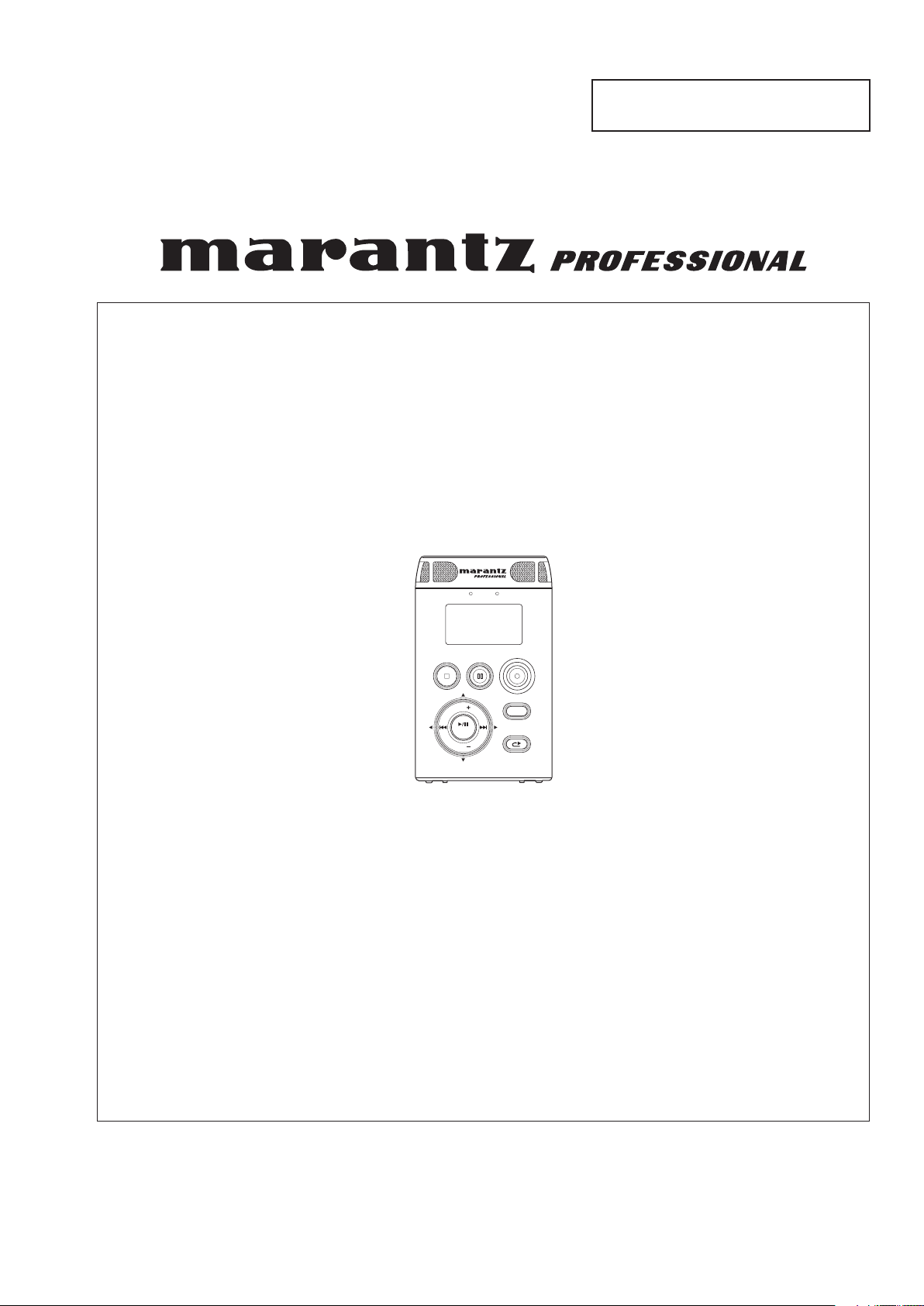
PMD620
Handheld Solid State Recorder
LEVEL OVER
REC
REC PAUSESTOP/CANCEL
VOL
ENTER
VOL
SOLID STATE RECORDER
Please use this service manual with referring to the user guide ( D.F.U. ) without fail.
修理の際は、必ず取扱説明書を準備し操作方法を確認の上作業を行ってください。
DISPLAY
MENU/STORE
SKIP BACK
PMD620
D&M Holdings Inc.
PROFESSIONAL BUSINESS COMPANY
KAYABACHOTOWER,1-21-2SHINKAWA,CHUO-KU,TOKYO104-0033JAPAN
Telephone:03(6731)5588
Part no. 00M10CS855010
First Issue 2007.11
Page 2

SECTION PAG E
TABLE OF CONTENTS
1. TECHNICAL SPECIFICATIONS ..................................................................................................... 1
2. SERVICE MENU ............................................................................................................................ 2
2.1. OLED Check ........................................................................................................................... 2
2.2 LED Check ............................................................................................................................. 3
2.3 Door Sence ............................................................................................................................. 3
2.4 Heat Run ................................................................................................................................ 4
2.5 Factory Default ....................................................................................................................... 4
3. HOW TO DISASSEMBLE .............................................................................................................. 5
4. Version update ................................................................................................................................8
5. BLOCK DIAGRAM .......................................................................................................................... 9
6. SCHEMATIC DIAGRAM ................................................................................................................11
7. PARTS LOCATION ....................................................................................................................... 21
8. EXPLODED VIEW AND PARTS LIST .......................................................................................... 25
9. IC DATA ........................................................................................................................................ 29
10. ELECTRICAL PARTS LIST .......................................................................................................... 54
The exchange of the lithium battery(Z701 : CR1220/IFC).
CAUTION
Danger of explosion if battery is incorrectly replaced.
Replace only with the same or equivalent type.
リチウム電池
(Z701 : CR1220/IFC)
の交換について
注意
電池を誤って交換すると爆発する危険があります。
同一又は同等の型のものにのみ交換してください。
Page 3

1. TECHNICAL SPECIFICATIONS
Digital Audio System
System ..................................................Solid State Recorder
Usable media ...............................................SD/SDHC cards
Recording format
MP3 ....................................MPEG1 Layer
WAV ..................................................16/24 bit linear PCM
Recording MP3 bit-rate
Stereo ......................................................192/128/64 kbps
Mono ........................................................... 96/64/32 kbps
Sample rate ........................................................44.1/48 kHz
Number of channels .............................. 2 (Stereo)/1 (Mono)
III
Compression
Audio Performance
Frequency response .......................... 20 Hz - 20 kHz (±1dB)
S/N ratio IEC-A weighted
MIC ........................................................................... 68 dB
LINE ......................................................................... 80 dB
Total harmonic distortion at 0 VU
MIC ...........................................................................0.06%
LINE .........................................................................0.02%
Dynamic range ............................................................ 81 dB
Inputs
External MIC
Type ..........................................................1/8" stereo jack
Input sensitivity ....................................6 mVrms/30 kohms
LINE
Type ..........................................................1/8" stereo jack
Input sensitivity ................................500 mVrms/20 kohms
General
Power consumption
Recording/Playback .........................................1.5 W (DC)
Battery life (Alkaline) ............................... 5 hours (Typical)
Phantom power .........................................5V, 1mA (Max.)
Environmental conditions
Operational temperature .................. 0 - 40°C (32 - 104°F)
Operational humidity ..............25 - 85% (no condensation)
Storage temperature .................... –20 - 60°C (–4 - 140°F)
Dimensions
Width .............................................................62 mm (2.5")
Height ............................................................. 102 mm (4")
Depth ................................................................25 mm (1")
Weight (Excl. batteries) ....................................110g (4 oz)
Included Accessories
Audio cable
USB cable
AC adapter
User guide
CD-ROM (U, N only)
Handy strap
Customer Registration Document (US only)
Tripod/Belt clip adapter
SD card
• Specifi cations are subject to change without notice.
Outputs
LINE
Type ..........................................................1/8" stereo jack
Standard level ...........................................1.0 V/10 kohms
Headphone
Type ..........................................................1/8" stereo jack
Standard level ..........................................16 mW/16 ohms
Speaker
Standard level ..........................................150 mW/8 ohms
1
Page 4
2. SERVICE MENU
2. SERVICE メニュー
<Service Menu Details>
<サービスメニューの内容>
DisplayMenu
表示メニュー
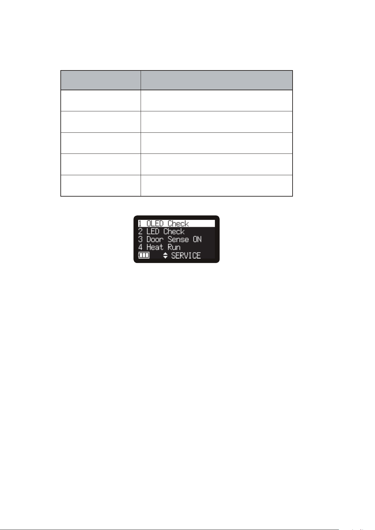
1 OLED Check
2 LED Check
3 Door Sense
4 Heat Run
5 Factory Default
ServiceDetails
サービス内容
Check the display section by lighting all OLED.
OLEDの全点灯により、表示部を確認します。
Check the LED by lighting all LED.
LEDの全点灯により、LEDを確認します。
Set the door sensor ON/OFF.
ドアセンサの ON/OFFを設定します。
Perform a heat run test by using continuous play.
連続再生によりヒートラン試験を行います。
Return to the factory default settings.
工場出荷状態に戻します。
2.1 OLED Check
1) Press the REC PAUSE button and REC LEVEL – button
at the same time, and turn the POWER slide switch ON.
At this time, the service menu list is displayed in the
display section.
2)
Press the VOL + and VOL – buttons to select “OLED Check”.
At this time, the selected menu item is highlighted.
3) If the 3/8/ENTER button is pressed, all of the OLED
light.
• If the 4 button is pressed while all OLEDs are lit,
the display returns to the service menu list.
• If the 3/8/
are lit, the display returns to the service menu list.
ENTER
button is pressed while all OLEDs
2.1 OLED チェック
REC PAUSE
1)
押しながら、
とき、表示部にサービスメニュー一覧が表示されます。
VOL +
2)
Check” を選 択します。このとき、選択したメニュ ーが
ハイライト表示されます。
3) 3/8/
•
OLEDが全点灯中に 4ボタンを押すと、サービス
メニュー一覧に戻ります。
•
OLEDが全点灯中に 3/8/
ビスメニュー一覧に戻ります。
ボタンと
POWER slide
ボタンおよび
ENTER
ボタンを押すと、OLEDが全点灯します。
REC LEVEL −
スイッチを Onします。この
VOL –
ボタンを押して、“OLED
ENTER
ボタンを同 時に
ボタンを押すと、サー
2
Page 5

2.2 LED Check
1) Press the REC PAUSE button and REC LEVEL – button
at the same time, and turn the POWER slide switch ON.
At this time, the service menu list is displayed in the
display section.
2) Press the VOL + and VOL – buttons to select “LED Check”.
At this time, the selected menu item is highlighted.
2.2 LED チェック
REC PAUSE
1)
押しながら、
とき、表示部にサービスメニュー一覧が表示されます。
VOL +
2)
Check” を選 択します。このとき、選択したメニュ ーが
ハイライト表示されます。
ボタンと
POWER slide
ボタンおよび
REC LEVEL −
スイッチを Onします。この
VOL –
ボタンを押して、“LED
ボタンを同 時に
3) If the 3/8/ENTER button is pressed, “∗” is displayed on
the back of “LED Check”, and all LEDs light (REC, OVER,
LEVEL, REMOTE RED, REMOTE GREEN).
• If the 4 button is pressed while all LEDs are lit, all
LEDs go off, and the display returns to the service
menu list.
• If the 3/8/
are lit, all LEDs go off, the “∗” display switches off, and
the display returns to the service menu list.
ENTER
button is pressed while all LEDs
2.3 Door Sence
1) Press the REC PAUSE button and REC LEVEL – button
at the same time, and turn the POWER slide switch ON.
At this time, the service menu list is displayed in the
display section.
2) Press the VOL + and VOL – buttons to select “Door Sence”.
At this time, the selected menu item is highlighted.
ENTER
3) 3/8/
の後ろに“∗”が表示され、LEDが全点灯(REC、 OVER、
LEVEL、 REMOTE RED、 REMOTE GREEN)します。
•
LEDが全点灯中に 4ボタンを押すと、LED を全消灯
させ、サービスメニュー一覧に戻ります。
•
LEDが全点灯中に 3/8/
を全消灯させ、“∗” 表示を消灯しサービスメニュー一覧
に戻ります。
ボタンを押すと、メニュ ーの“LED Check”
ENTER
ボタンを押すと、LED
2.3 ドアセンサの設定
REC PAUSE
1)
押しながら、
とき、表示部にサービスメニュー一覧が表示されます。
VOL +
2)
ON” を選択します。このとき、選択したメニューがハイ
ライト表示されます。
ボタンと
POWER slide
ボタンおよび
REC LEVEL −
スイッチを Onします。この
VOL –
ボタンを押して、“Door Sense
ボタンを同 時に
3) If the 3/8/ENTER button is pressed, the PMD620 sensor
is set to OFF.
• At this time, “Executing…” is displayed in the display
section.
• If the settings are completed, “Completed” is
displayed in the display section for 1 second, the
display returns to the service menu and “Door Sense
OFF” is displayed.
If the 3/8/ENTER button is pressed while “Door Sense
OFF” is displayed, the PMD620 sensor is set to ON.
ENTER
3) 3/8/
状態に設定します。
•
このとき、表示部に“Executing...”が表示されます。
•
設定が完了すると、表示部に “Completed”が1 秒間
表示され、サービスメニューに戻り “Door Sense OFF”
が表示されます。
“Door Sense OFF” 表 示しているときに 3/8/
ボタンを押すと、PMD620をセンサON状態に設定します。
ボタンを押すと、PMD620 をセンサOFF
ENTER
3
Page 6

2.4 Heat Run
1) Press the REC PAUSE button and REC LEVEL – button
at the same time, and turn the POWER slide switch ON.
At this time, the service menu list is displayed in the
display section.
2) Press the VOL + and VOL – buttons to select “Heat Run”.
At this time, the selected menu item is highlighted.
2.4 ヒートラン実行
REC PAUSE
1)
押しながら、
とき、表示部にサービスメニュー一覧が表示されます。
VOL +
2)
Run” を選択します。 このとき、選 択したメニューが
ハイライト表示されます。
ボタンと
POWER slide
ボタンおよび
REC LEVEL −
スイッチを Onします。この
VOL –
ボタンを押して、“Heat
ボタンを同 時に
3) If the 3/8/ENTER button is pressed, continuous play
starts.
• During continuous play, all switches other than the
POWER slide
• During playback, if playback continues to the fi nal fi le,
all fi les are repeated and playback continues from the
fi rst fi le.
• If an error occurs during continuous playback, the
display remains in the error display status.
switch are inactive.
2.5 Factory Default
1) Press the REC PAUSE button and REC LEVEL – button
at the same time, and turn the POWER slide switch ON.
At this time, the service menu list is displayed in the
display section.
2) Press the VOL + and VOL – buttons to select “Factory
Default?”. At this time, the selected menu item is
highlighted.
3) If the 3 /8 /ENTER button is pressed “Default?” is
displayed in the display section.
4) While “Default?” is being displayed, press the 4 button
and select “YES”.
5) If the 3/8/ENTER button is pressed “Executing…” fl ashes
in the display section.
• When the settings have returned to the factory default
settings, “Completed” is displayed for 1 second, after
which the display section returns to the service menu.
• When the settings have been returned to the factory
default settings, the “Date Form” default setting is the
setting for the US. This needs to be set correctly for
the destination.
“Date Form”
US : M/D/Y
Europe : D/M/Y
6) Turn the POWER slide switch OFF.
3) 3/8/
ENTER
•
連続再生中は、
•
連続再生では、最後のファイルまで再生が実行すると、
最初のファイルへ戻りオールリピートします。
•
連続再生中にエラーが発生したときは、エラー表示状態
のままになります。
ボタンを押すと、連続再生が始まります。
POWER slide
スイッチ以外は無効です。
2.5 工場出荷状態へ戻す
REC PAUSE
1)
押しながら、
とき、表示部にサービスメニュー一覧が表示されます。
VOL +
2)
Default?” を選択します。このとき、選択したメニューが
ハイライト表示されます。
3) 3/8/
4) “Default?”が表示中に、
5) 3/8/
6)
ENTER
されます。
選択します。
ENTER
点滅表示されます。
•
工場出荷状態への設定が完了すると、表示部に
“Completed”が1秒間表示され、サービスメニューに戻
ります。
•
工場出荷状態へ戻した場合、“Date Form” のデフォルト
設定はUS向けの設定となります。出荷先に応じた設
定が必要です。
“Date Form”
US : M/D/Y
Europe : D/M/Y
POWER slide
ボタンと
POWER slide
ボタンおよび
ボタンを押すと、表示部に“Default?”が表示
ボタンを押すと、表示部に “Executing...”が
スイッチを OFFします。
REC LEVEL −
スイッチを Onします。この
VOL –
ボタンを押して、“Factory
4
ボタンを押して、“YES”を
ボタンを同 時に
4
Page 7
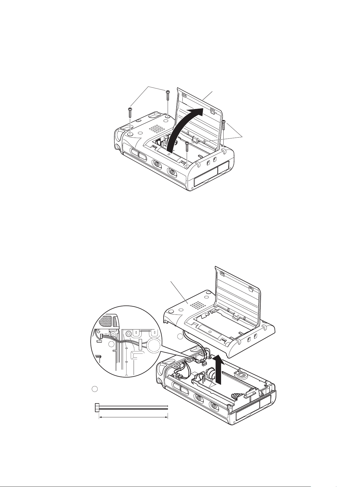
3. HOW TO DISASSEMBLE
Lch
J611
SPK
J609
3. 分解方法
1) Open the battery cover on the back of the main unit, and
remove the 4 “A” screws.
A
1) 本体背面のバッテリーカバーを開き、ネジA 4本を外し
ます。
Battery cover
A
2) Lift the rear block slowly in the direction of the arrows,
disconnect the speaker cable q connector from J609 as
shown in the diagram below to remove the rear block.
Rear block
1
1 Speaker cable
00MYB00067520 (W003)
P2
P1
63mm
Red
Black
2) リアブロックをゆっくり矢印の方向へ持ち上げ、下図の
ようにスピーカケーブルqのコネクタ 1ヶ所をJ609か
ら外すと、リアブロックが取り外せます。
1
5
Page 8
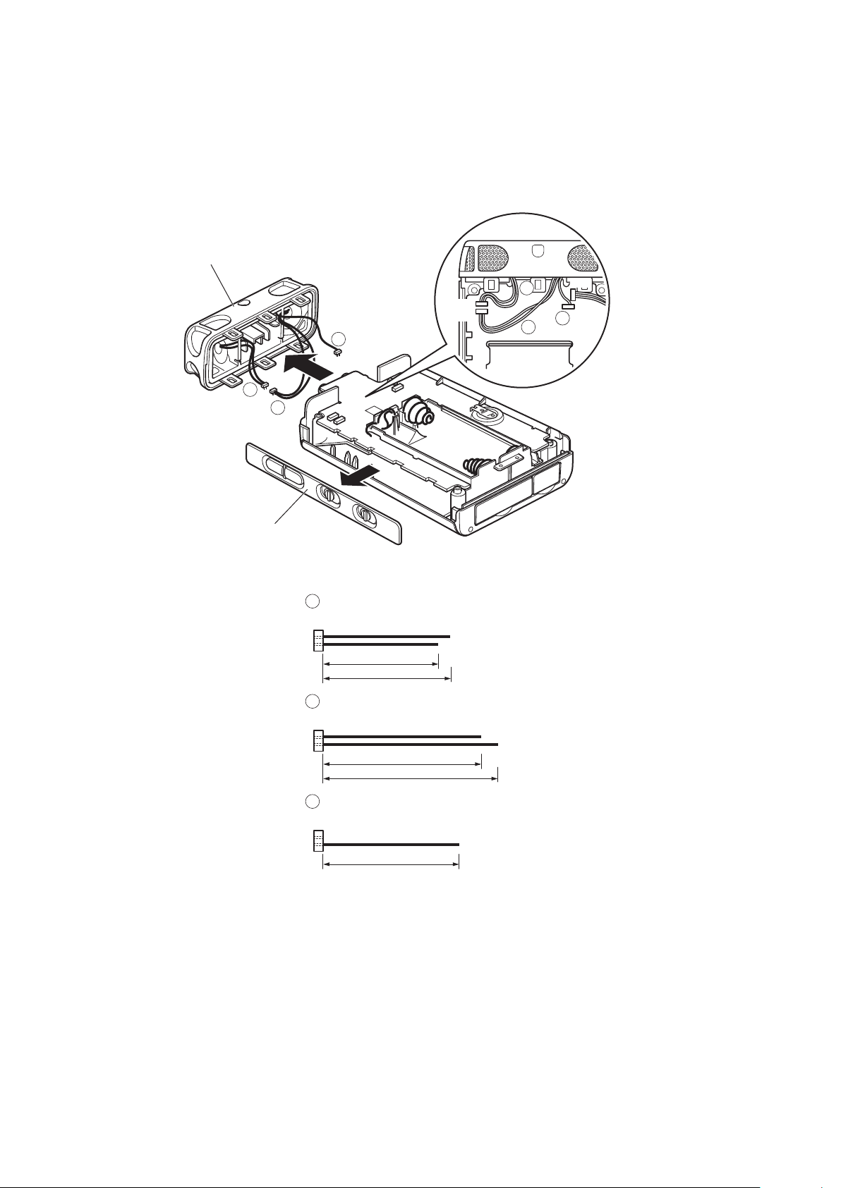
3) As shown in the diagram below, disconnect the Mic
Rch Lch
J608
J607
J611
J609
Rch cable 2 connector from J608, the Mic Lch cable
3 connector from J607, and the Mic shield cable r
connector from J611, and the top block can now be
removed. Also remove the button side block in the
direction of the arrow.
Top block
4
2
3
3) 下図のように Mic Rchケーブルwのコネクタを J608か
ら外し、Mic Lch ケーブルeのコネクタをJ607から外し、
Mic シールドケーブルrのコネクタを J611から外すと、
トップブロックが取り外せます。またボタンサイドブ
ロックも矢印方向に取り外します。
2
4
3
Button side block
2 Mic Rch cable
P2
P1
3 Mic Lch cable
P2
P1
4 Mic shield cable
P2
P1
00MYB00051800 (W002)
Black
45mm
50mm
Black
00MYB00067540 (W001)
63mm
68mm
00MYB00051790 (W004)
Black
53mm
Black
Black
6
Page 9
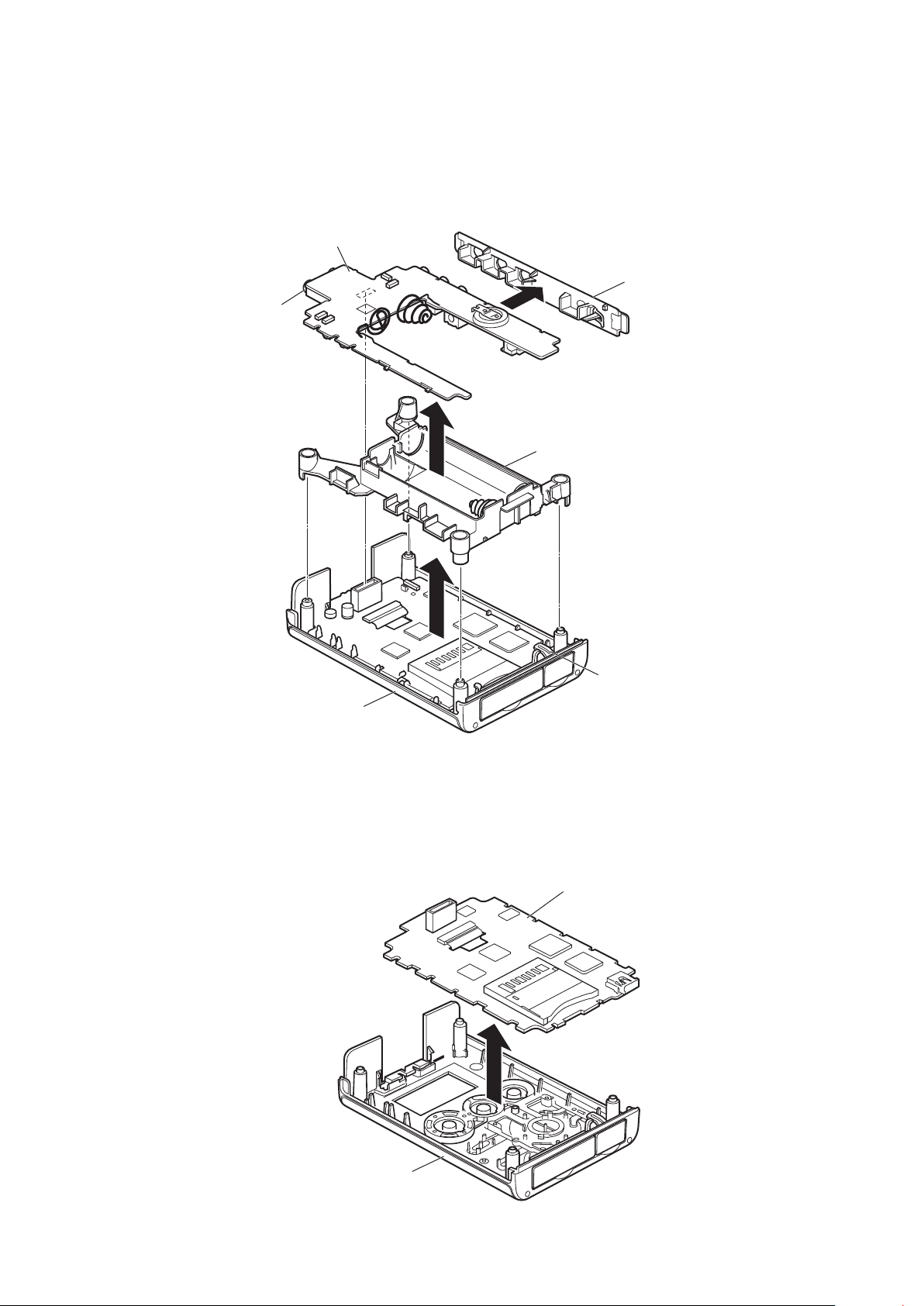
k
4) Lift the P102 jack section, and remove the P102 board
from the battery block in the direction of the arrow. Also,
the jack side block can be removed. The battery block
is held in place by the foot of the USB cap. Remove the
USB cap foot, and remove the battery block from the front
block in the direction of the arrow.
P102 PWB
Jacks
4) P102のジャック部 分を持ち上げてバッテリブロックか
ら P102基板を矢印 方向に取り外します。またジャック
サイドブロックも取り外せます。USBキャップの足で
バッテリブロックが固定されています。この USBキャッ
プの足を外して、フロントブロックからバッテリブロッ
クを矢印方向に取り外します。
Jack side bloc
Battery block
Front block
5) Remove the P101 board from the front block in the
direction of the arrow, as shown in the diagram below.
USB cap
5) 下図のようにフロントブロックから P101基板を矢印方
向に取り外します。
P101 PWB
Front block
7
Page 10

4. Version Update
4. SDカードからのバージョンアップ方法
1) Insert the SD card for updating into the loading slot of the
main unit.
2) Turn the POWER slide switch ON. At this time, “Update
A-XXX?” is displayed in the display section.
If this is not displayed, perform steps 5) ~ 7) and check
the version.
3) Press the 4 button, and select “YES”.
4) If the 3/8/ENTER button is pressed “Executing…” fl ashes
in the display section, and update begins.
When update has completed, the system automatically
restarts.
5) To check the current main unit version, press the MENU
button for 3 seconds. At this time, the menu list is
displayed in the display section.
Press the VOL + and VOL – buttons to select “F/W Version”.
6)
At this time, the selected menu item is highlighted.
7) If the 3/8/ENTER button is pressed, the current version
is displayed in the display section.
8) Turn the POWER slide switch OFF.
1) アップデート用のSDカードを本 体の挿入口に差し込み
ます。
POWER slide
2)
に“Up date A-XXX?”が表示されます。
表示されないときは、手順 5)〜7)を操作してバージョン
を確認してください。
4
3)
ボタンを押して、“YES”を選択します。
4) 3/8/
アップデートが完了すると、自動的に再起動します。
5) 現在の本体のバージョンを確認するには、MENUボタン
6)
7) 3/8/
8)
ENTER
点滅表示され、アップデートが始まります。
を 3秒間押します。このとき、表示部にメニュー一覧が
表示されます。
VOL +
Version” を選択します。このとき、選択したメニューが
ハイライト表示されます。
ENTER
が表示されます。
POWER slide
スイッチを Onします。このとき、表示部
ボタンを押すと、表示部に “Executing...”が
ボタンおよび
ボタンを押すと、表示部に現在のバージョン
スイッチを OFFします。
VOL –
ボタンを押して、“F/W
8
Page 11
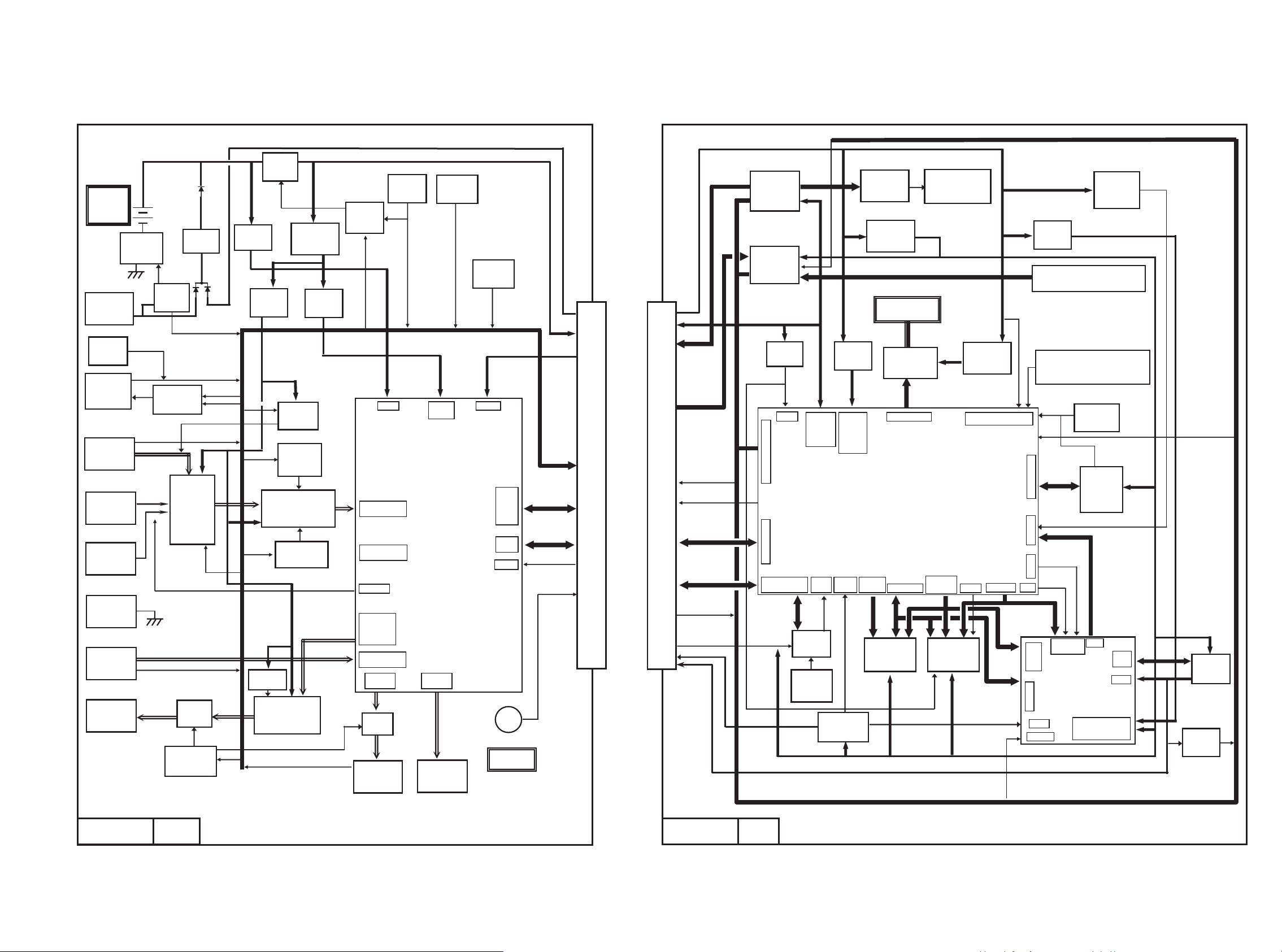
5. BLOCK DIAGRAM
9 10
Q 412
CODEC
TLV320AIC 32
Q 001
DSP
TM S320VC 5509A
Q005
SDRAM
Q006
FLASH MEM
J203
USB
JACK
J607
INTERNAL
MIC-Lch
J603
EXTERNAL
MIC IN
J606
LINE-IN
J605
LINE-OUT
J604
HP-OUT
J609
SP-OUT
(MONO)
J201
SD CARD
SLOT
A/D
J701
MIC
REMOTE
DATA0〜3
CLK
CMD
MMC1
OLED
SSD1305T6R1
ADDRESS
BUS
DATA BUS
SDA10
SDRAS#
SDCAS#
SDWE#
CE2#
Q311
RTC
I2C
COIN TYPE
BATTERY
Z701
INT2
GPIO
Q202
P-IN S-OUT
SHIFT
RESISTER
OE#,WE#
McBSP0
RTC_INT#
SDRAM
I/F
SDA
SCL
D201〜D206
LED
REC/LEVEL/PEAK
SDA
SCL
GPIO〔8:0〕
D〔15:0〕
Q613
BATT SW
Q608
3.3V REG
Q607
1.8V REG
Q303
1.2V REG
Q604
5V DC-DC
CONVERTER
BAT_MON
Q617
3.3V REG
CVDD
RCVDD
RDVDD
USBPLL
VDD
USBVDD
DVDD
ADVDD
AVDD
RESET
Q201
S-IN P-OUT
SHIFT
RESISTER
USB
VBUS5V
IOVDDDVDD
DC IN
5V
HPLOUT
HPROUT
HPLCOM
HPRCOM
LEFT_LOP
LEFT_LOM
RIGHT_LOP
RIGHT_LOM
MIC2L/LINE2L
MIC2R/LINE2R
MIC3L/LINE3L
MIC3R/LINE3R
MIC BIAS
BATTERY
AA or
NIMH
X2
A〔20:0〕
AIN〔3:0〕
D3.3V 1.2V
D3.3V
RESET#
A3.3V
1.8V
W/P_SW
INS_SW
Q004
RESET
DRVDD
AVDD
Q207
USB CONTROLLER
M 66592
X301
XTAL
32.768KHz
DATA
ADDRESS
BUS
D〔15:0〕
A〔5:0〕
DHP
DHM
CE1#
CE1#
CS# RD#
WR0# WR1#
INTCE0#
INT
Q002
OSCILLATOR
12MHz
X2/
CLKIN
X1
RESET_N
VBUS
XIN
AFEAVDD AFEDVDD
BIASVDD PLLVDD
VDD(CORE) VIF
McBSP2
SYS_RST#
J608
INTERNAL
MIC-Rch
Q405
ADG736
MIC SW
J611
MIC EARTH
Q551
MUTE
Q614
POW SW
Q415
4.6V REG
J610 B TO B CONNECTOR
EXTMIC_DET
LINEIN_DET
MIC_ATT1,2
Q414,510,511
MUTE DRIVER
HP_DET
MUTE_CONT
Q705,706
LED DRIVER
REMO_KEY
LED_GRN
LED_RED
RESET
SDA
SCL
BCLK
DIN
DOUT
WCLK
MCLK
BCLK
DIN
DOUT
WCLK
CLK12M
SDA
SCL
CODEC__RST#
MIC_SEL
RTC_VCC
S701
LEVEL-
SW
S702
LEVEL+
SW
Q612
DC_DET
SW
DC_IN
Q501
NJM2737RB1
LINE-OUT AMP
Q408,Q426
LOW CUT
FILTER
LCF_CONT
MIC1L/LINE1L
MIC1R/LINE1R
Q611
NJM2737RB1
MIC AMP
Q406,407,Q411
MIC ATT
P_ON
J301 B TO B CONNECTOR
CR1220/1FC
Q304
3.3V DC-DC
CONVERTER
J204
OLED
CONNECTOR
RTC_VCC
CLK_12M
Q301
12V DC-DC
CONVERTER
Q203,204
LED DRIVER
REMO_KEY
REMO_KEY
Q302
1.5V REG
BCLK
DIN
DOUT
WCLK
POW_CONT
1
MUTE_CONT
MIC_ATT1
MIC_ATT2
MIC_SEL
CODEC_RST#
MICBIAS CON
LCF_CONT
LED_RED
LED_GRN
HP_DET
DC_DET
KEY_LOCK
P_ON
EXTMIC_DET
LININ_DET
P_CONT1
CLK,DATA,STB,SYS_RST#
Q083
VIN _LOW
_DET
Q502
MIC BIAS
S703
POWER
SW
S704
KEY LOCK
SW
D3.3V
VIN
USB
VBUS5V
12V
1.5V
VIN
D3.3V
SUB PW B MAIN PWBP102 P101
4.6V
5V
RE
S001〜S007
DISPLAY/ >>/<</PLAY
/SKIPBACK/VOL+/VOL- KEY
S203
SD COVER
SW
CLK ,DATA,STB
Q208
VBUS
DET
Q514,515
MUTE
VBUS_DET
Q427
MIC BIAS
SW
Q615,D61
2
WAKE
J601
DC JACK
EX001〜EX003
REC/RECPAUSE/STOP KEY
MICBIAS_CON
Page 12
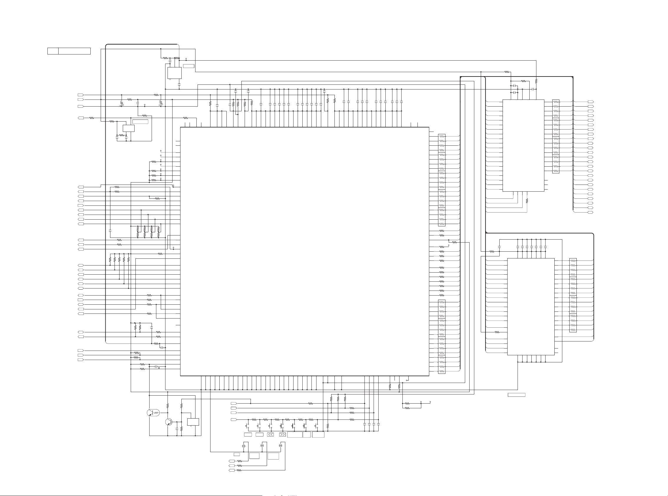
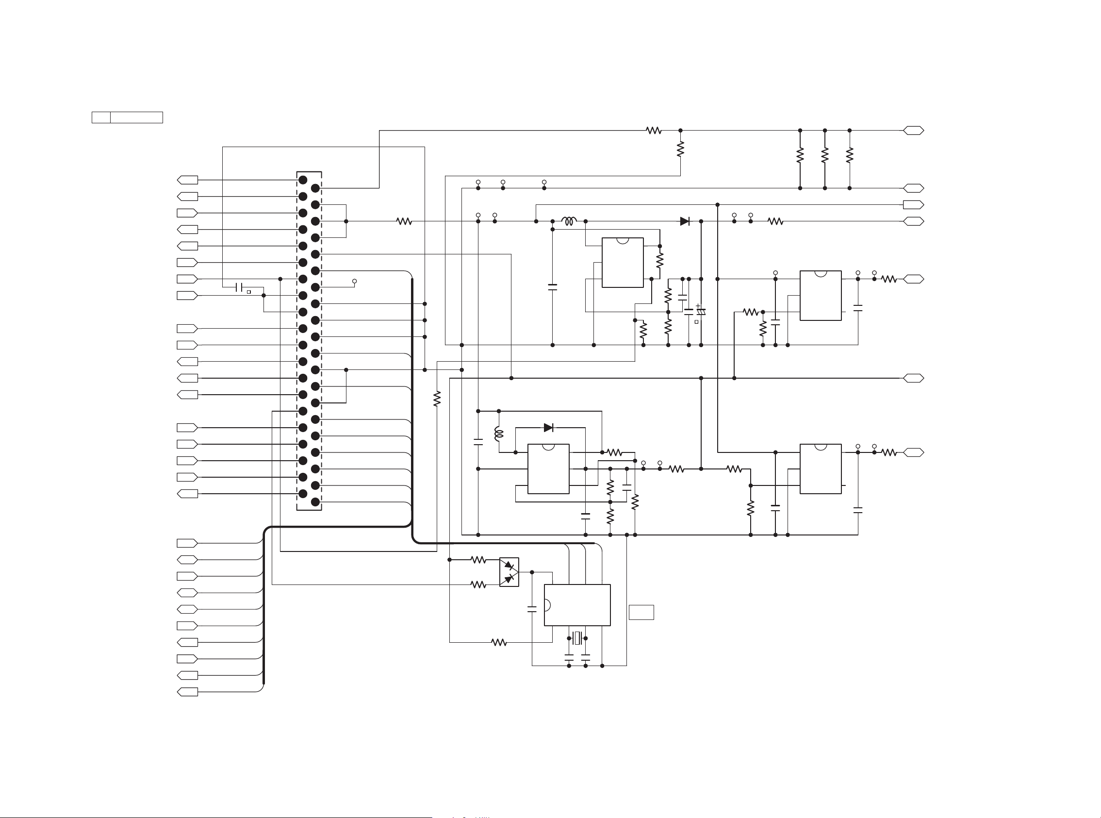
6. SCHEMATIC DIAGRAM
11 12
OE#
0.1u
C021
R066
0
C015
22u
R105 22
R111
22
1243
8765
DGND
SD_DATA0
C133
0.1u
A5
0.1u
C017
0
R184
RTC_INT#
BCLK
D15
33
R037
P_CONT1
S004
SKRMABE010
12
DIN
100k
R107
0.1u
C011
R182
0
R093
22
12
43
8765
D11
R102 22
C071
0.1u
1k
R186
R029
82k
R069
22k
Q002
DSO321SR
12.0MHz
±
50ppm
4
Vdd3OUT
1
CONT2GND
R109 22
R047
1k
R095
22
1243
8765
470
R075
NM
R055
D13
2200p
C078
0.1u
C036
SR-CLK
0.1u
C014
CLK_12M
D4
R134
22
1243
8765
C132
0.1u
D/C#
D10
KEY_STO P
C137
0.1u
R099 22
TP009
SDIN
T
C041
NM
33
R038
100k
R006
REMO_KEY
R104 22
SD_SW
0.1u
C024
R028
82k
EX001
12
470p
C074
SD_DATA3
S007
SKRMABE010
12
0.1u
C022
SD_DATA1
S002
SKRMABE010
12
R092
22
1243
8765
TP011
100k
R007
0.1u
C027
R174
10k
A2
0.1u
C032
TP002
TP101
R098 22
S003
SKRMABE010
12
0.1u
C026
R106 22
R140
22
1243
8765
R113
22
1243
8765
SRO-STB
R064 0
SD_DATA2
R024
0
R096 22
D12
D1
R136
22
1243
8765
C122
0.1u
NM
R018
TP004
R034
NM
100kR057
C131
0.1u
R070
47k
C135
0.1u
0.1u
C013
C003
0.1u
0
R052
TP010
R010
220k
C077
1u
0.1u
C016
10k
R073
A6
100k
R017
0
R183
0.1u
C031
100k
R019
R081
6.8k
R065
0
0.1u
C033
R097 22
SCK
SRI-DATA
C134
0.1u
C006
1u
0
R061
NM
R021
100
R089
1.2V
100k
R022
0
R051
C136
0.1u
R063 0
TP007
NM
C004
0.1u
C040
R060
0
R103 22
100k
R008
100k
R015
TP100
R135
22
1243
8765
SD_CLK
0.1u
C034
470p
C072
0.1u
C025
SDA
D0
0.1u
C023
R115
22
1243
8765
R175
10k
C121
4.7u
R142
22
1243
8765
0
R121
R082
12k
0.1u
C018
A1
A3
R077
1.5k
R080
3.9k
SS#
EX002
12
D3
470p
C073
R078
1.8k
100k
R009
0.1u
C038
33
R036
SRI-STB
WCLK
R114
22
1243
8765
D2
0.1u
C035
0.1u
C019
WE#
1k
R187
S001
SKRMABE010
12
SYS_RST#
R032 47k
S006
SKRMABE010
12
SD_CMD
T
22U/4V
C028
R138
22
1243
8765
R131
0
R043
4.7k
R090
10k
0.1u
C037
100kR058
D14
TP105
R112
22
1243
8765
DOU T
Q004
PST-3629NR
1
OUT2VDD3GND
4NC5
Cd
R027
220k
SCL
1k
R188
D7
R123
1k
10k
R072
TP003
470
R074
D5
EX003
12
R101 22
C130
4.7u
0
R025
0
R122
R005
33
100k
R056
R044
4.7k
R124
0
R033
1k
MUTE_CON T
TP005
KEY_REC
TP044
R137
22
1243
8765
R002
33
D6
D8
0.1u
C042
R059
0
KEY_LEV+
RE#
BAT_MO N
TP006
R030
82k
NM
R020
S005
SKRMABE010
12
0.1u
C020
C123
1u
R062 0
10k
R071
D9
470
R076
CE0#
R141
22
1243
8765
33
R035
R079
2.7k
A4
R108 22
R094
22
1243
8765
L001
0
0.1u
C012
R003
10k
NM
R016
0.1u
C030
R132
0
SRO-DATA
TP008
R031
82k
SOF
INT0#
D3.3V
R067
0
R100 22
0.1u
C039
R045
0.1u
10u
C029
KEY_R-PAUS
Q005
MT48LC4M16A2B4-7E
G3
A9
H9
A10
G2
A11
G7
BA0
G8
BA1
CLK
F2
CKE
F3
H8
A1
J8
A2
J7
A3
J3
A4
J2
A5
A1
VSS1
CAS#
F7
RAS#
F8
WE #
F9
H3
A6
H2
A7
H1
A8
CS#
G9
E3
VSS2J1VSS3A3VSSQ1
C3
VSSQ 2B7VSSQ 3D7VSSQ 4
NC1
G1
NC2
E2
DQML
E8
F1
DQMH
A2
DQ15
B1
DQ14
B2
DQ13
C1
DQ12
C2
DQ11
D1
DQ10
D2
DQ9
E1
DQ8
E9
DQ7
D8
DQ6
D9
DQ5
C8
DQ4
C9
DQ3
B8
DQ2
B9
DQ1
A8
DQ0
VDD1
A9
H7
A0
VDD2E7VDD3
J9
VDDQ 1A7VDDQ 2B3VDDQ 3C7VDDQ 4
D3
Q001
TMS320VC5509AZHH
RTCINX2
B12
RTCINX1
A12
TRST#
J12
TCK
J13
TDI
K14
TDO
K13
TMS
J14
EMU0
K11
EMU1/OFF
K12
GPIO8/RE#
G5
GPIO 7
D1
GPIO 6
C4
GPIO 5
D5
GPIO 4
A3
GPIO 3
B3
GPIO2
E2
GPIO1
E1
GPIO 0
F3
MMC2_DAT3/FSX2
D10
MMC2_DAT0/CLKX2
B10
MMC2_CLK/DX2
A11
MMC2_DAT2/FSR2
C9
MMC2_DAT1/DR 2
A10
MMC2_CMD/CLKR2
A9
MMC1_DAT3/FSX1
E8
MMC1_DAT0/CLKX1
C8
MMC1_CLK/DX1
E9
MMC1_DAT2/FSR1
A7
MMC1_DAT1/DR1
D8
MMC1_CMD/CLKR1
D7
CLKR0
B5
DR0
D6
FSR0
A5
CLKX0
C6
DX0
E7
FSX0
B6
TIN/TOUT
B4
SDA
H13
SCL
H14
RESET#
H12
INT0#
G14
INT1#
G13
INT2#
G10
INT3#
F14
INT4#
F12
VSS1B1VSS2C2VSS3E4VSS4F4VSS5N2VSS6P2VSS7M3VSS8M5VSS9
N14
VSS10
M13
VSS11
D11
VSS12
C11
VSS13
B11
VSS14B9VSS15K4VSS16K5VSS17N1VSS18P1VSS19N9VSS20
N10
VSS21
F11
VSS22
E13
VSS23C7VSS24C5VSS25E5VSS26A2AVSS1
C13
AVSS2
B14
ADVSS
E12
USBPLLVSS
G12
AN3
E11
AN2
D12
AN1
D13
AN0
D14
DN(USB)D3PU(USB)C1DP(USB)
D4
XF
E14
D0
L8
D1
K8
D2
P9
D3
M9
D4
L9
D5
P10
D6
M10
D7
P11
D8
N11
D9
L10
D10
P12
D11
N12
D12
M14
D13
L11
D14
L12
D15
L13
BE1#
K2
BE0#
J4
SDWE#
L3
SDCAS #
K3
SDRAS#/GPIO12
M1
SDA10/GPIO13
M2
CLKMEM
L2
CE0#/GPIO 9
H4
CE1#/GPIO10
H5
CE2#
J1
CE3#/GPIO11
J3
RDY
H1
WE#
G4
OE#
G2
A20
G3
A19
H3
A18
K1
A17
P5
A16
P7
A15
M8
A14
K9
A13
N3
A12
P3
A11
L4
A10
N4
A9
P4
A8
L5
A7
N5
A6
L6
A5
M6
A3
K6
A4
P6
A2
K7
A1
M7
A0
L7
A’0
H11
CLKOUT
F5
CVDD13
C10
CVDD14
L1
CVDD15
J5
CVDD 1B2CVDD 2M4CVDD 3
L14
CVDD 4
J10
CVDD5
J11
CVDD6
M11
CVDD7
G1
CVDD8
N7
CVDD9
N8
CVDD10
B8
CVDD11
B7
CVDD12
A6
USBPLL_VDD
G11
DVDD1
E3
DVDD2
N6
DVDD3
F13
DVDD4
A8
DVDD5
H10
DVDD6
D9
DVDD7
H2
DVDD8
J2
DVDD9
P8
DVDD10
K10
DVDD11
E6
DVDD12
A4
DVDD13
P13
DVDD14
N13
DVDD15
M12
DVDD16
P14
USBVDD
D2
ADVDD
F10
AVDD
C14
RDVDD1
B13
RDVDD2
A13
RDVDD3
A14
RCVDD
C12
X1
F1
X2/CLKIN
F2
NC
E10
NC
C3
Q006
S29AL016D70BFI020
C5
A10
A5
A9
B5
A8
A2
A7
C2
A6
D2
A5
B1
A4
C3
A18
B2
A17
E6
A16
D6
A15
C6
A14
F1
CE#
E1
A0
D1
A1
C1
A2
A6
A13
B6
A12
D5
A11
A1
A3
G1
OE#A4WE #A3RY/BY#
B3
NC1
C4
NC2
D3
NC3
E2
DQ0
H2
DQ1
E3
DQ2
H3
DQ3
H4
DQ4
E4
DQ5
H5
DQ6
E5
DQ7
F2
DQ8
G2
DQ9
F3
DQ10
G3
DQ11
F4
DQ12
G5
DQ13
F5
DQ14
G6
DQ15
B4
RESET#
F6
BYTE #
H6
VSS1H1VSS2
G4
VCC
D4
A19
Q083
NJU7700F4-/F15
4
VSS3NC
1
VOU T2VDD
Q082
NM
Q081
NM
1
2
3
TP102
C051
0.01u
NM
R085
C081
NM
NM
R084
0
R083
D0
D1
D2
D3
D4
D5
D6
D7
D8
D9
D10
D11
D12
D13
D14
D15
A1
A2
A3
A4
A5
A6
CE0#
OE#
D8
WE #
RST#
A1
A2
A3
A4
A7
A6
A8
A5
A9
A10
A12
A11
A14
A15
A16
A13
A20
A19
A18
A17
D13
D12
D15
D14
D4
D5
D2
D0
D3
D9
D6
D1
D10
D11
D7
A20
A19
A18
A17
A16
A15
A14
A13
A12
A11
A10
A9
A8
A7
A6
A5
A4
A3
A2
A1
RST#
RY
OE#
WE #
CE1#
A1
A2
A3
A4
A5
A6
A7
A8
A9
A10
SDA1 0
A12
A13
A14
CLKMEM
CE2#
SDWE #
RAS#
CAS#
BE1 #
BE0 #
D12
D8
D5
D3
D14
D10
D7
D11
D13
D4
D15
D6
D9
D0
D1
D2
OE#
WE #
CE2#
CE1#
CE0#
CLKME M
SDA10
RAS#
CAS#
SDWE #
BE0#
BE1#
RY
D15
D0
D8
D13
D2
D7
D12
D9
D4
D11
D5
D10
D6
D14
D1
D3
1.2V
DGND
SDRAM64M
RESET
OSCIRATO R
DSP
REC REC
DISPLAY
PAUSE
/MEN U
STOP/
CANCEL
SKIP
BACK
PLAY/PAUSE
ENTER
VOL+VOL-
MAIN UNIT
P101 00MWI10CS1010
Page 13
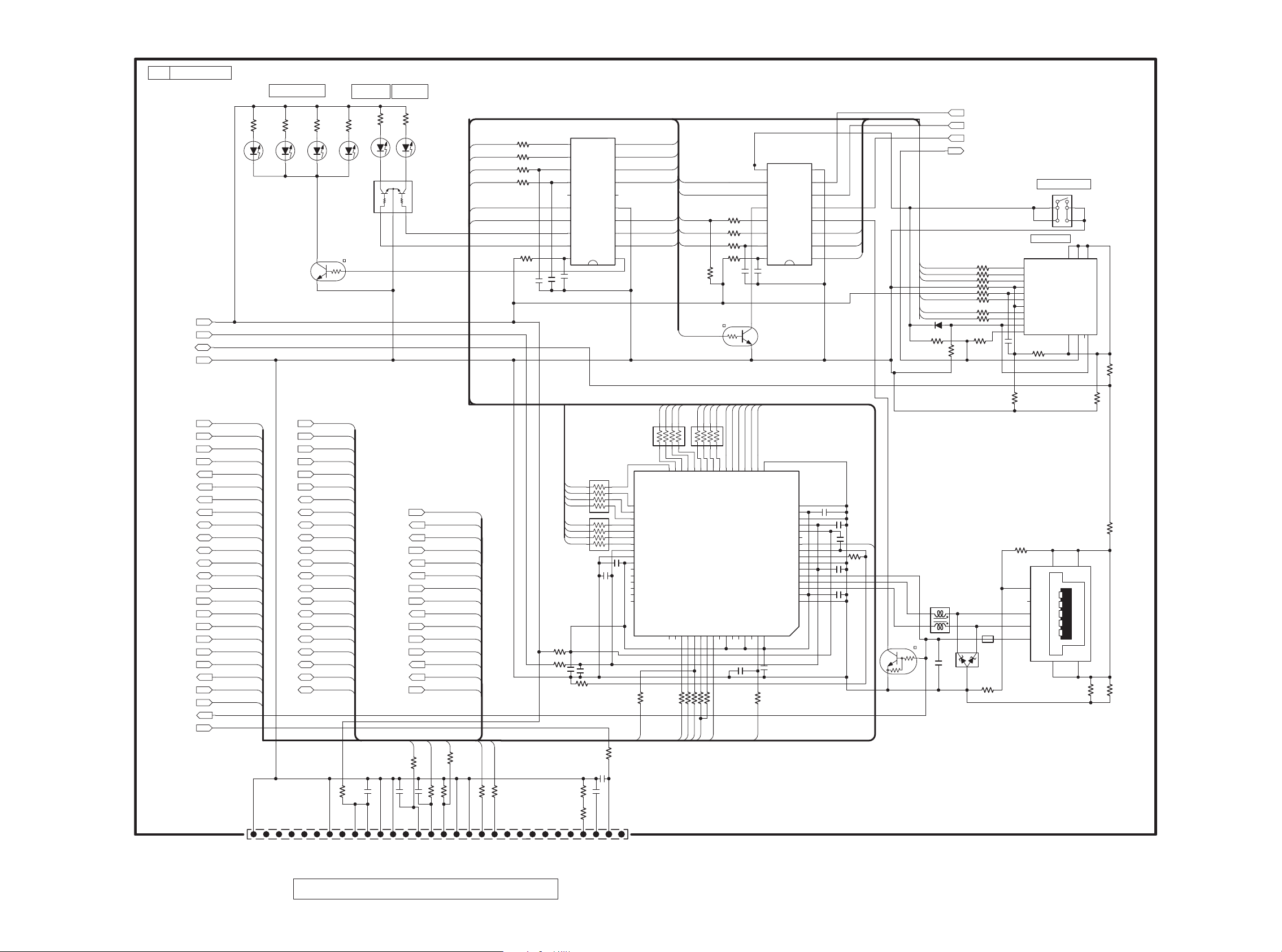
13 14
NJU3713A
Q201
1
P5
2
P6
3
P7
4
P8
5
VSS
6
NC
7
P9
8
P10
9
P11
10
P12
11
DATA
12
CLK
13
STB#
14
CLR #
15
NC
16
P1
17
P2
18
P3
19
P4
20
VDD
Q202
NJU3754
1
P0
2
P1
3
P2
4
P3
5
P4
6
P5
7
P6
8
VS S
9
P7
10
P8
11
P9
12
P10
13
SO
14
CLK
15
CE #
16
VDD
A1
A3
EXTMIC_DET
LININ_DET
SCK
A2
D3.3V
DGND
1.5V
HP_DET
DC_DET
SD_CLK
A6
SDIN
A4
SYS_RST#
SRO-STB
SR-CLK
SRO-DATA
SRI-STB
CLK_12M
15V
OE#
WE #
CE0#
D/C#
A5
SS#
P_ON
KEY_REC
KEY_R-PAUS
KEY_STOP
KEY_LOCK
RE#
D205
SML-512M W
12
D206
SML-511UW
12
D204
SML-511U W
12
D203
SML-511UW
12
D202
SML-511UW
12
D201
SML-511U W
12
Q207
M66592FP
1
AFED33G
2
AFED33V
3
DM
4
DP
5
VBUS
6
AFEA15V
7
AFEA15G
8
REFRIN
9
AFEA33G
10
XIN
11
XOUT
12
AFEA33V
13
AFED15V
14
AFED15G
15
VIF
16
TEST
17
MPBUS
18A119A220A321A422A523
A6/ALE
24D025D126D227D328D429D530D631D732
D8
33
D9
34
D10
35
D11
36
D12
37
D13
38
D14
39
D15
40
VDD
41
DGN D
42
VIF
43
SDO
44
SD1
45
SD2
46
SD3
47
SD4
48
SD5
49
SD650SD7
51
INT_N
52
SOF_N
53
RD_N
54
WR0_N55WR1_N
56
CS_N
57
DREQ0_N
58
DACK0_N
59
DEND0_N
60
DREQ1_N
61
DACK1_N/DSTB0_N
62
DEND1_N
63
RST_N
64
VIF
NMR275
NM
R230
R201
470
R202
470
R203
470
R204
470
R205
470
R206
270
0
R215
0
R216
0
R218
1k
R217
0
R250
0
R226
0
R227
0
R229
1k
R228
0
R252
0
R244
R249
NM
6.8k
R251
12k
R248
R207
0
R209
0
R208
0
0
R294
0
R293
0
R240
0
R296
0R297
0
R2990R300
5.6k
R261
0
R271
0
R280
0
R274
0
R2780R279
0
R285
820k
R284
220k
R283
0
R281
1k
R295
F263
0
NM
R298
0
R291
0
R232
0
R231
0
F255
0
R221
0
R222
33
R242
33
R243
33
R245
33
R246
33
R247
33
R241
4.7u
C281
25V
4.7u
C282
25V
0.1u
C211
C212
0.1u
0.1u
C275
0.1u
C274
C278
0.1u
0.1u
C271
0.1u
C272
0.1u
C263
0.1u
C273
C277
0.1u
C213
100p
0.01u
C215
4.7u
C291
10u
C292
4.7u
C279
1000p
C283
4.7u
C264
C214
100p
C276
1u
NM
C284
C253
NM
Q208
DTC144EMT2L
1
2
3
MICBIAS_CON
MIC_ATT1
MIC_ATT2
LCF_CONT
P_CONT2
SRI-DATA
VBUS
INT0#
SO F
LED_RED
LED_GRN
CODEC_RST#
SD_SW
MIC_SEL
D0
D1
D2
D3
D4
D5
D6
D7
D8
D9
D10
D11
D12
D13
D14
D15
SD_DATA0
SD_DATA3
SD_DATA2
SD_DATA1
SD_CM D
FG
EMG3T2R
Q203
123
45
Q204
DTC114TMT2L
1
2
3
Q610
DTC114TMT2L
1
2
3
D241
RB520S-30TE61
F261
DLP11SN161SL2
1
3
4
2
D261
NSAD500F
1
2
3
TP221
R288 22
12 43
8765
R287 22
12 43
8765
R289 22
1243
8765
R290 22
1243
8765
J204
04 6238 030 010 868+
30
NC
29
VCC
28
VCOM H
27
IREF
26
D7
25
D6
24
D5
23
D4
22
D3
21
D2
20
D1/SDIN
19
D0/SCLK
18
E(RD#)
17
R/W #
16
D/C#
15
RES#
14
CS#
13
FR
12
BS2
11
BS1
10
VDDIO
9
VDD
8
NC
7
GND
6
NC
5
NC
4
NC
3
NC
2
NC
1
VSS
F262
BLM21PG221SN1D
S203
SPVP110100
13
24
J201
SDKR-9BRS-K13-G
3 SD.VSS1
2 SD.CMD
1 SD.DAT3
9 SD.DAT2
SD.VDD4
SD.CLK5
SD.VSS26
SD.DAT07
8 SD.DAT1
11 COM1
10 INS
12
WP
13
COM 2
14GND
GND
15
GND
16
GND
17
CSS 5005-0402F
J203
4
ID
3
D+
2
D-
1
VBUS
5
GND
SR-CLK
CLK_12M
INT0#
SOF
OE#
SYS_RST#
WE #
SD_DATA1
SD_DATA0
SD_CLK
SD_CMD
SD_DATA3
SD_DATA2
SDIN
SCK
SYS_RST#
DC_DET
HP_DET
LININ_DET
EXTMIC_DET
MIC_ATT1
LCF_CONT
MICBIAS_CON
SD_DATA3
SD_DATA2
SD_DATA0
SD_DATA1
SD_CM D
SD_CLK
SCK
SDIN
SYS_RST#
SRO-STB
SRI-STB
SRO-DATA
SRI-DATA
SR-CLK
CLK_12M
A1
A2
A3
A4
A6
D0
D1
D2
D3
D4
D5
D6
D7
D8
D9
D10
D11
D12
D13
D14
D15
SYS_RST#
SRO-STB
SR-CLK
SRO-DATA
MIC_ATT2
A5
SS#
HP_DE T
A1
A6
D0D1D2
D3
D4D5D6
D7
D9
D10
D11
D12
D13
D14
SRI-STB
EXTMIC_DET
LININ_DET
KEY_LOCK
DC_DE T
P_O N
D15
D8
A4A5A3
A2
D/C#
MIC_ATT1
MIC_ATT2
CODEC_RST#
LED_RED
LED_GRN
P_CONT2
MICBIAS_CON
LCF_CONT
CE0#
CODEC_RST#
KEY_LOCK
LED_GRN
LED_RED
SS#
P_O N
P_CONT2
OE #
WE #
CE0#
INT0#
SOF
D/C#
MIC_SEL
MIC_SEL
SRI-DATA
RE#
RE#
SD COVER SW
OLED ASSY
REC_LEVELPEAK LEVEL
LED-RED LED-GREEN
REC LED-RED
SD SLO T
MAIN UNIT
P101 00MWI10CS1010
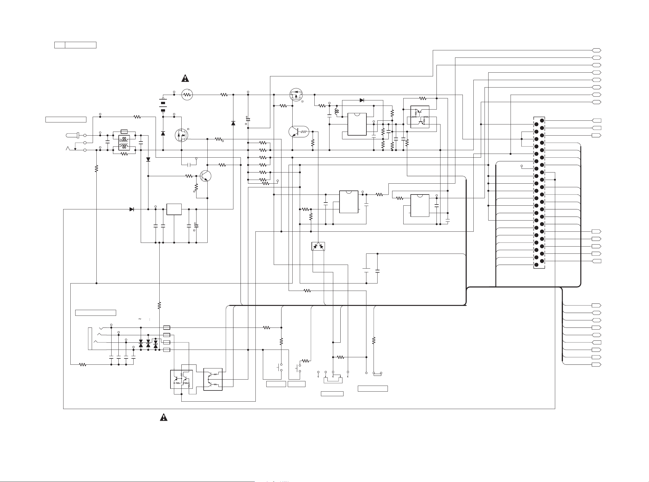
Page 14
15 16
TP301
TP311
TP312
TP322
TP302
TP303
TP304
TP305 TP346
TP345
TP341
TP342
TP343
TP344
TP333
R305
110K
R304
NM
R322
NM
R332
NM
R341
NM
R312
NM
R317
NM
R301
0
R307
0
R302
100k
R306
1M
R311
10k
R313
0
R323
0
R321
10k
R331
100k
R333
560k
R334
330k
R315
10k
R316
1.2k
L302
0
R342
0
R343
0
R351
0
R352
0
R353
0
L301
10uH
L331
4.7uH
C311
1u
C321
1u
NM
C315
0.1u
C317
C331
4.7u
C332
4.7u
C301
10u
C312
4.7u
C322
10u
C304
0.1u
C302
10p
C313
47p
5p
C316
J301
40P9.0JMCS-G-B-TF
1
21
2
22
3
23
4
24
5
25
6
26
7
27
8
28
9
29
10
30
11
31
12
32
13
33
14
34
15
35
16
36
17
37
18
38
19
39
20
40
Q303
XC6210B122M
1
VIN
2
VSS
3
CE
4
NC
5
VOUT
Q302
XC6210B152M
1
VIN
2
VSS
3
CE
4
NC
5
VOU T
Q301 LT1615ES5
1
SW 1
2
GND
3
FB4#SHDN
5
VIN
Q304
LTC3400BES6
1
SW
2
GND
3
FB
4
SHDN
5
VOUT
6
VIN
FG
15V
SDA
WCLK
1.2V
D3.3V
1.5V
DGND
BCLK
P_ON
KEY_LOCK
DC_DET
REMO_KEY
KEY_LEV+
EXTMIC_DET
DOUT
LININ_DET
HP_DET
BAT_MON
RTC_INT#
MIC_SEL
P_CONT1
P_CONT2
CODEC_RST#
LCF_CONT
MIC_ATT2
MUTE_CONT
LED_GRN
LED_RED
SCL
CLK_12M
MICBIAS_CON
MIC_ATT1
DIN
VBUS
S-35390A-I8TG 1
Q311
1
INT1#2XOUT3XIN4VSS
5
INT2#
6
SCL
7
SDA
8
VDD
D311
DAN222MT2L
1
2
3
X301
SSP-T6 32.768KHz
± 10ppm
12
D301
RB551V-30TE-17
D331 RB551V-30TE-17
C303
10u/25V
C305
0.01u
CODEC_RST#
BCLK
WCLK
DOUT
DIN
SCL
SDA
CODEC_RST#
DIN
SCL
WCLK
DOUT
CLK_12M
CLK_12M
SDA
BCLK
VIN
RTC_INT#
SCL
SDA
D3.3V
RTC_INT#
RTC_VCC
MIC_SEL
MIC_SEL
RTC
MAIN UNIT
P101 00MWI10CS1010
Page 15
17 18
D701
RSB6.8GT2R
D702
RSB6.8GT2R
D703
RSB6.8GT2R
Q613
Si2312BDS
2
3
1
S704
SSSS710607
KEY_LOCK_SW
123
S703
SSSS7A0202
POWER_SW
23C41
Q705
EMB11T2R
145
326
Q614
Si2333DS
2
3
1
Z701
CR1220/1FC
1
2
Q617
BA33BC0FP-E2
IN
1
GND
2
OUT
3
Q605
NM
123
456
Q612
2SC5658T2L
J601
HEC3600-010110
1
3
2
J701
HSJ1637-010512
1
4
2
3
D604
RB161VA-20
D601
RR264M-400TR
D603
RR264M-400TR
D602
RB161VA-20
D605
RB551V-30TE-17
R605
NM
R632
NM
R614
NM
R662
0
R615
1k
56k
R616
R603
0
R604
0
R618
0
R747
220k
R749
220k
R667
0
R745
10k
R633
1M
R609
100k
R704
0
R634
100k
R611
0
R607
22k
R606
15k
R746
1k
R751
220k
R752
39k
R750
0
2.2k
R706
R701
0
F602
0
R748
0
C604
0
R610
0
R619
0
R608
0
R702
NM
R631
330k
C602
1u
C631
1u
1uC605
C704
NM
C614
NM
C633
1u
C636
0.1u
C621
4.7u
C622
4.7u
C632
4.7u
C701
100p
C702
100p
C703
100p
C624
22U
C623
22U
C634
4.7u
C606
NM
C635
47p
C607
1000p
C608
1000p
Q607
XC6210B182M
1
VIN
2
VS S
3
CE
4
NC
5
VOUT
Q608
XC6210B332P
1
VIN
2
VSS
3
CE
4
NC
5
VOUT
L603
4.7uH
DIN
MUTE_CON T
CLK_12M
CODEC_RST#
SCL
MICBIAS_CON
LCF_CONT
MIC_ATT1
MIC_ATT2
MIC_SEL
HP_DE T
EXTMIC_DET
DOUT
LININ_DET
F601
BLM21PG221SN1D
F701
BLM15BD102SN1D
F702
BLM15BD102SN1D
F703
BLM15BD102SN1D
F704
BLM15BD102SN1D
AGND
DGND
5V
1.8V
BCLK
WCLK
SDA
A3.3V
D3.3V
FG
GN D
Q604
LTC3400BES6
1
SW
2
GND
3
FB
4
SHDN
5
VOUT
6
VIN
TP604
TP608
BAT+
TP609 BAT-
TP611
TP614
TP605
TP610
TP603
TP701
TP702
TP703
TP704
TP601
TP602
TP705
TP706
TP615
TP607
TP612
TP606
S701
SKRELJE010
LEVEL-
12
S702
SKRELJE010
LEVEL+
12
EMG3T2R
Q706
123
45
Q615
DTC114TMT2L
1
2
3
F603
NM
1
4
3
2
D612
DAN222MT2L
123
J610
40R-JMCS-G-B-TF
1
21
2
22
3
23
4
24
5
25
6
26
7
27
8
28
9
29
10
30
11
31
12
32
13
33
14
34
15
35
16
36
17
37
18
38
19
39
20
40
C603
47u/6.3V
C601
100U/10V
t
nanoSMDC150F
J602
2.2k
R602
18k
R617
KEY_LEV+
BCLK
DIN
WCLK
DOUT
CLK_12M
CODEC_RST#
LED_RED
LED_GRN
KEY_LOCK
DC_IN
REMO_KEY
P_CONT1
VBUS
P_CONT2
LED_GRN
RTC_VCC
LED_RED
KEY_LOCK
KEY_LEV+
SD A
SC L
DIN
DOUT
WCLK
CLK_12M
BCLK
CODEC_RST#
VIN
VIN
SD A
SC L
P_CONT1
P_ON
P_ON
REMO_KEY
MIC_SEL
LDO3.3V
DC_IN
RTC_VCC
MIC_SEL
P_CONT2
F604 607
MIC REMOTE JACK
"NOTE ON SAFETY: The parts marked with are IMPORTANT PARTS on the safety.
Please use the parts having the designated parts number without fail"
DC JACK
SUB UNIT
P102 00MWI10CS1020
Page 16

19 20
D421
RSB6.8GT2R
D422
RSB6.8GT2R
D452
RSB6.8GT2R
D451
RSB6.8GT2R
D402
RSB6.8GT2R
D401
RSB6.8GT2R
D501
RSB6.8GT2R
D502
RSB6.8GT2R
D551
RSB6.8GT2R
D552
RSB6.8GT2R
D581
RSB6.8GT2R
D582
RSB6.8GT2R
R555
NM
R556
NM
R525
NM
R526
NM
R477
NM
R478
NM
R414
NM
R415
NM
1k
R439
F400
0
2.2k
R404
2.2k
R403
R406
220k
220k
R407
220k
R455
220k
R456
R755
1k
R441
100
R440
100
R453
2.2k
R454
2.2k
F450
0
R412
4.7k
R413
180k
R429
180k
R430
4.7k
R419
270k
R423
470k
R422
22k
47k
R437
47k
R438
47k
R499
R483
3.3k
R484
3.3k
R482
15k
R481
15k
1k
R487
F480
0
R497
0
R496
0
R4950R4940R4930R492
0
R6130R612
0
R581 0
R582 0
F550
0
1k
R591
F500
0
R523
22k
R524
22k
R521
0
R522
0
R516
220k
R515
220k
R517
200
R518
200
R514
220k
R513
220k
R511
33k
R512
33k
R505
22k
R501
22k
R502
22k
R506
22k
R503
22k
R507
22k
R504
22k
R508
22k
R510
33k
R509
33k
R559
220k
R520
4.7k
R410
15k
R411
56k
R431
56k
R432
15k
R462
2.2M
R461
2.2M
R528
NM
R527
100k
L491
0
L492
0
R553
4.7
R554
4.7
R551
100
R552
100
R485
2.2k
R486
2.2k
R498
0
R463
0
R408
1k
R409
1k
R457
1k
R458
1k
R443
0
R445
NM
R442
NM
R444
NM
C475
NM
C464
NM
C410
1u
C401
22u
C553
NM
C554
NM
C441
1u
C440
22u
C513
NM
C415
NM
C416
NM
C479
NM
C480
NM
C417
1u
C491
0.1u
C497
0.1u
C496
0.1u
C495
0.1u
C494 0.1u
C514
NM
C492
10u
C498
10u
C506
10p
C505
10p
C503
10p
C504
10p
C502
68p
C501
68p
C509
10u
C510
10u
C511
10u
C507
10u
C481
220p
C482
220p
C451
4.7u
C452
4.7u
C403
4.7u
C402
4.7u
C406
4.7u
C407
4.7u
C404
2p
C409
2p
C408
4p
C405
4p
4.7u
C413
4.7u
C414
C484
10u
C483
10u
C512
1u
C443
1u
C493
1u
C418
1u
C420
0.1u
C419
0.1u
C485
100p
C486
100p
0.01u
C411
0.01u
C412
C478
470p
C477
470p
C476
470p
C472
470p
C473
470p
C467
470p
C469
470p
C465
470p
470p
C466
C474
470p
C471
100p
C468
100p
Q411
EMH2T2R
123
456
Q404
2SC5658T2L
NJM2737RB1 1/2
Q611
2
3
1
4
Q501
NJM2737RB1 1/2
2
3
1
4
Q501
NJM2737RB1 2/2
6
5
7
8
Q611
NJM2737RB1 2/2
6
5
7
8
TLV320AIC32
Q412
1MCLK
2BCLK
3WCL K
4DIN
5DOUT
6DVSS
7IOVDD
8SCL
12 MIC2L
13 MIC2R
14 MIC3L
15 MICBIAS
16 MIC3R
17 AVSS1
18 DRVDD1
19 HPLOUT
20 HPLCOM
21 DRVSS
22 HPRCOM
23 HPROUT
24 DRVDD2
25AVDD
26AVSS2
27LEFT_LOP
28LAEFT_LOM
29RIGHT_LOP
30RIGHT_LOM
31RESET
32DVDD
11 MIC1R
9 SDA
10 MIC1L
5V
AGND
DIN
DGND
1.8V
A3.3V
D3.3V
MICBIAS_CON
LCF_CON T
MIC_ATT1
MIC_ATT2
MUTE_CON T
CLK_12M
CODEC_RST#
SCL
MIC_SEL
GND
BCLK
WCLK
SDA
FG
DOUT
EXTMIC_DET
LININ_DE T
HP_DET
Q426
DTC144EMT2L
1
2
3
Q427
DTC144EMTL2
1
2
3
Q510
DTC144EMT2L
1
2
3
J606
LGY3009-0200F
LINE-IN
1
4
6
5
3
2
J605
LGY3009-0200F
LINEOU T
1
4
6
5
3
2
J607
24 8000 002 000 829+
MIC-L
1
2
J609
24 8000 002 000 829+
1
2
J608
24 8000 002 000 829+
MIC-R
1
2
J611
24 8000 002 000 829+
1
2
F581
BLM15BD102SN1D
F582
BLM15BD102SN1D
F552
BLM15BD102SN1D
F551
BLM15BD102SN1D
F503
BLM15BD102SN1D
F501
BLM15BD102SN1D
F482
BLM15BD102SN1D
F481
BLM15BD102SN1D
F452
BLM15BD102SN1D
F451
BLM15BD102SN1D
F402
BLM15BD102SN1D
F401
BLM15BD102SN1D
F442
BLM15BD102SN1D
F441
BLM15BD102SN1D
Q406
EMA4T2R
123
45
Q407
EMA4T2R
123
45
Q514
US6K2
123
456
Q551
US6K2
123
456
TP404
TP405
TP406
TP408
TP409
TP411
TP410
TP412
TP413
TP414
TP415
TP416
TP417
TP418
TP419
TP420
TP424
TP426
TP427
TP425
Q412
33
ADG736
Q405
12345
678 910
Q414
EMD2T2R
123
456
EMB3T2RQ408
123
456
Q502
NJU7009
123
45
Q413
EMB2T2R
145
326
Q515
UMG3NTR
123
4
5
T
C552
220u 4V
T
C551
220u 4V
Q415
XC6210B452M
1
VIN
2
VSS
3
CE
4
NC
5
VOUT
Q511
2SA2029
1
2
3
J604
LGY2209-0300F
HP
1
2
3
4
J603
LGY2209-0300F
EXTERNAL MI C
1
2
3
4
Q581
NM
123
456
R491 0
R420
12k
R421
12k
CODEC_RST#
BCLK
DIN
WCL K
DOUT
EXTMIC_DET
MICBIAS_CON
LCF_CON T
LININ_DET
MIC_ATT1CLK_12M
CODEC_RST#
SC L
SD A
MIC_ATT1
MIC_ATT2
LCF_CONT
LININ_DET
EXTMIC_DET
MIC_ATT2
MUTE_CONT
SCL
SDA
DOUT
DIN
WCLK
BCLK
CLK_12M
MIC_SEL
MIC_SEL
MICBIAS_CO N
AGND_IN
MUTE_CON T
5V
AGND_OUT
SUB UNIT
P102 00MWI10CS1020
Page 17

21 22
P101 B
7. PARTS LOCATION
P101 A
C003 A2
C004 A2
C011 A2
C012 A2
C014 A2
C032 A2
C051 A1
C081 A1
C211 B2
C212 B1
C214 B1
C264 A2
C276 A1
C279 B1
C281 B1
C282 B1
C283 B1
C284 B1
C301 B1
C303 B1
C305 C1
C311 B1
C313 A1
C317 B2
C321 B1
D241 B1
D261 B2
D301 B1
D311 B2
D331 A1
F255 A1
F261 A2
F262 A1
F263 A2
J201 A1
J203 A2
J204 B1
J301 B1
L001 A2
L301 B1
L302 A1
L331 A1
Q001 A2
Q002 A2
Q005 A1
Q006 A1
Q081 A1
Q082 A1
Q083 A1
Q201 B2
Q202 B1
Q203 C1
Q204 A2
Q207 A2
Q208 A2
Q301 B1
Q302 B1
Q303 A1
Q304 A1
Q311 B2
Q610 C1
R002 A2
R003 A2
R005 A2
R024 A2
R025 A2
R027 A2
R033 A2
R034 A2
R035 A2
R036 A2
R037 A2
R038 A2
R061 A2
R062 A2
R064 A2
R083 A1
R084 A1
R085 A1
R092 A1
R093 A1
R094 A1
R095 A1
R096 A1
R097 A1
R098 A1
R099 A1
R100 A1
R101 A1
R102 A1
R103 A1
R104 A1
R105 A1
R106 A1
R107 A2
R108 A1
R109 A2
R111 A1
R112 A1
R113 A1
R114 A1
R115 A1
R134 A1
R135 A1
R136 A1
R137 A1
R138 A1
R140 A1
R141 A1
R142 A1
R182 A2
R207 B1
R208 B2
R209 B2
R229 B1
R231 A1
R232 A1
R248 A1
R249 A1
R250 B2
R251 B1
R261 A2
R271 B1
R274 B1
R275 B1
R278 A1
R279 A1
R280 B1
R281 B1
R283 B1
R284 B1
R285 B1
R287 B2
R288 A2
R289 A2
R290 A2
R295 A1
R296 A1
R297 A1
R298 A1
R299 A1
R300 A1
R307 B1
R311 B1
R312 B1
R313 B1
R321 A1
R322 A1
R323 A1
R331 A1
R332 A1
R333 A1
R334 A1
X301 B2
C006 A2
C013 A2
C015 A1
C016 A1
C017 A2
C018 A2
C019 A2
C020 A1
C021 A1
C022 A2
C023 A2
C024 A2
C025 A2
C026 A1
C027 A2
C028 A2
C029 A2
C030 A2
C031 A1
C033 A1
C034 A2
C035 A2
C036 A1
C037 A2
C038 A2
C039 A1
C040 A2
C041 A2
C042 A2
C071 A1
C072 A1
C073 A1
C074 A1
C077 A2
C078 A2
C121 A1
C122 A1
C123 A1
C130 A1
C131 A1
C132 A1
C133 A1
C134 A1
C135 A1
C136 A1
C137 A1
C213 B2
C215 B2
C253 A1
C263 A2
C271 A1
C272 A2
C273 A2
C274 A2
C275 A2
C277 A2
C278 A1
C291 B2
C292 B2
C302 B1
C304 B1
C312 B1
C315 B2
C316 B2
C322 B1
C331 A1
C332 A1
D201 A1
D202 A1
D203 A1
D204 A1
D205 B1
D206 B1
EX00 A1
EX00 A1
EX00 A2
Q004 A2
R006 A1
R007 A1
R008 A1
R009 A1
R010 A2
R015 A2
R016 A2
R017 A2
R018 A2
R019 A2
R020 A2
R021 A2
R022 A2
R028 A1
R029 A1
R030 A1
R031 A1
R032 A1
R043 A1
R044 A1
R045 A2
R047 A2
R051 A1
R052 A1
R055 A1
R056 A1
R057 A1
R058 A1
R059 A2
R060 A2
R063 A2
R065 A1
R066 A2
R067 A2
R069 A1
R070 A1
R071 A1
R072 A1
R073 A1
R074 A1
R075 A1
R076 A1
R077 A1
R078 A1
R079 A1
R080 A1
R081 A2
R082 A1
R089 A2
R090 A2
R121 A1
R122 A1
R123 A1
R124 A1
R131 A1
R132 A1
R174 A2
R175 A2
R183 A1
R184 A1
R186 A1
R187 A1
R188 A2
R201 A1
R202 A1
R203 A1
R204 A1
R205 B1
R206 B1
R215 B2
R216 B2
R217 B2
R218 B2
R221 B1
R222 B2
R226 B2
R227 B1
R228 B1
R230 B2
R240 A2
R241 A1
R242 A1
R243 A1
R244 A1
R245 A1
R246 A1
R247 A1
R252 A1
R291 A1
R293 A1
R294 A2
R301 B1
R302 B1
R304 B1
R305 B1
R306 B1
R315 B2
R316 B2
R317 B2
R341 B1
R342 C1
R343 C1
R351 C2
R352 C1
R353 C1
S001 A1
S002 A1
S003 A1
S004 A1
S005 A2
S006 A1
S007 A1
S203 A1
鉛フリー半田
半田付けには、鉛フリー半田 (Sn-Ag-Cu) を使用してください。
Lead-free Solder
When soldering, use the Lead-free Solder (Sn-Ag-Cu).
Page 18

鉛フリー半田
半田付けには、鉛フリー半田 (Sn-Ag-Cu) を使用してください。
Lead-free Solder
When soldering, use the Lead-free Solder (Sn-Ag-Cu).
23 24
P102 B
C401 B2
C406 B2
C407 B2
C410 B1
C411 B1
C412 B2
C413 B1
C414 B1
C415 B1
C416 B1
C441 B2
C451 B2
C452 B2
C464 C1
C465 C1
C466 C1
C467 A1
C468 A0
C469 A1
C471 B1
C472 B1
C473 B0
C474 B1
C475 C1
C476 C1
C477 C1
C478 C1
C485 B1
C486 B1
C491 B1
C492 B1
C497 B1
C507 B1
C509 B1
C512 B1
C513 A1
C514 A1
C553 C1
C554 C1
C602 A1
C604 B2
C605 B1
C606 B1
C614 A1
C621 A2
C622 A2
C624 A2
C631 B1
C632 B1
C634 A2
C635 A2
C636 A1
C701 A1
C702 A1
C703 A1
C704 A1
D401 B1
D402 B1
D421 B1
D422 B1
D501 A1
D502 A1
D551 C1
D552 C1
D581 B1
D582 B1
D612 A2
D701 A1
D702 A1
D703 A1
F400 B1
F401 B1
F402 B1
F480 B1
F481 B1
F482 B1
F501 B1
F550 C1
F551 C1
F552 C1
F581 B1
F582 B1
F601 B1
F602 B1
F603 B1
F701 A1
F702 A1
F703 A1
F704 A1
J602 A2
J607 B2
J608 B2
J609 B1
J611 B1
L491 B1
L492 B1
Q404 B2
Q408 B1
Q411 B1
Q412 B1
Q413 B1
Q414 B1
Q427 B2
Q502 B1
Q510 B1
Q511 B1
Q514 B1
Q515 B1
Q551 B1
Q581 B1
Q604 A2
Q605 A2
Q607 B1
Q614 B2
Q615 B2
R403 B1
R404 B1
R414 B1
R415 B1
R419 B2
R420 B2
R422 B1
R423 B1
R437 B1
R438 B1
R439 C1
R440 B2
R441 B2
R444 A1
R455 B2
R456 B2
R463 B1
R481 B1
R482 B1
R485 B1
R486 B1
R487 B1
R503 A1
R504 B1
R513 B1
R514 B1
R520 B1
R521 B1
R522 B1
R523 B1
R525 A1
R526 A1
R527 B1
R528 B1
R551 C1
R552 C1
R553 C1
R554 C1
R555 C1
R556 C1
R559 A1
R581 B1
R582 B1
R591 C1
R605 A1
R606 B1
R607 B1
R609 A2
R611 B1
R613 B1
R614 B1
R618 B1
R619 B1
R632 A2
R633 A2
R662 A2
R701 A0
R702 A1
R704 A2
R706 A1
R745 A2
R746 A2
R747 A2
R748 A2
R749 B2
R751 B2
R755 B2
Z701 A1
P102 A
C402 B1
C403 B1
C404 B2
C405 B2
C408 B1
C409 B2
C417 B1
C418 B1
C419 B1
C420 B1
C440 B2
C443 B1
C479 B1
C480 B1
C481 B1
C482 B1
C483 B1
C484 B1
C493 B1
C494 B1
C495 B1
C496 B1
C498 B1
C501 B1
C502 A1
C503 B1
C504 B1
C505 B1
C506 A1
C510 B1
C511 A1
C551 C1
C552 C1
C601 B2
C603 A1
C607 A1
C608 A1
C623 A2
C633 A2
D451 B2
D452 B2
D601 B1
D602 A1
D603 A1
D604 A1
D605 A2
F441 B1
F442 B1
F450 B2
F451 B2
F452 B2
F500 B1
F503 B1
J601 A0
J603 C1
J604 C1
J605 A0
J606 B0
J610 B1
J701 A0
L603 A2
Q405 B1
Q406 B1
Q407 B1
Q415 B1
Q426 B1
Q501 B1
Q608 A2
Q611 B1
Q612 A1
Q613 A1
Q617 A1
Q705 A1
Q706 A1
R406 B1
R407 B1
R408 B1
R409 B1
R410 B2
R411 B2
R412 B2
R413 B2
R421 B1
R429 B1
R430 B1
R431 B1
R432 B1
R442 B1
R443 B1
R445 B1
R453 B2
R454 B2
R457 B2
R458 B2
R461 B1
R462 B1
R477 B1
R478 B1
R483 B1
R484 B1
R491 B1
R492 B1
R493 B1
R494 B1
R495 B1
R496 B1
R497 B1
R498 B1
R499 B1
R501 B1
R502 B1
R505 B1
R506 B1
R507 B1
R508 A1
R509 B1
R510 B1
R511 B1
R512 B1
R515 B1
R516 B1
R517 B1
R518 B1
R524 B1
R602 A1
R603 B1
R604 B1
R608 B2
R610 A1
R612 A1
R615 A1
R616 A1
R617 A1
R631 A2
R634 A2
R667 A2
R750 B2
R752 B2
S701 A2
S702 B2
S703 B2
S704 A2
Page 19

25 26
8. EXPLODED VIEW AND PARTS LIST
POS. NO. QTY
PART NO.
(FOR EUR)
PART NO.
(D&M)
PART NAME DESCRIPTION
001B 1 00M10CS064510 00M10CS064510 CASE ASSY TOP CASE ASSY
005B 1 00M10CS158010 00M10CS158010 WINDOW WINDOW
006B 1 00M10CS355020 00M10CS355020 LENS LED LENS
008B 1 00M10CS355010 00M10CS355010 LENS REC LENS
010B 2 00M10CS056010 00M10CS056010 BUFFER MIC BUFFER
012B 1 00M10CS270010 00M10CS270010 BUTTON TRACK JUMP BUTTON
014B 1 00M10CS270020 00M10CS270020 BUTTON REC BUTTON
016B 1 00M10CS270030 00M10CS270030 BUTTON ENTER BUTTON
018B 1 00M10CS257010 00M10CS257010 LID SD LID
020B 1 00M10CS257510 00M10CS257510 LID ASSY USB LID ASSY
026B 1 00M10CS271010 00M10CS271010 HOLDER OLED HOLDER
028B 1 00M10CS271020 00M10CS271020 HOLDER BATTERY HOLDER
030B 1 00M10CS123010 00M10CS123010 CONTACTOR RELAY CONTACTOR
032B 1 00M10CS249020 00M10CS249020 PANEL L SIDE PANEL
034B 1 00M10CS257500 00M10CS257500 LID ASSY DC JACK LID ASSY
038B 1 00M10CS249500 00M10CS249500 PANEL ASSY R SIDE PANEL ASSY
040B 1 00M10CS270040 00M10CS270040 BUTTON REC LEVEL BUTTON
044B 2 00M10CS271040 00M10CS271040 HOLDER MIC RUBBER HOLDER
048B 1 00M10CS271030 00M10CS271030 HOLDER MIC HOLDER
049B 1 00M10CS107010 00M10CS107010 SHEET MIC EARTH SHEET
050B 2 00M10CS202010 00M10CS202010 NET MIC NET
052B 1 00M10CS064020 00M10CS064020 CASE MIC CASE
053B 2 00M10CS107020 00M10CS107020 SHEET WIRE SHEET
001G 1 00M10CS064530 00M10CS064530 CASE ASSY BOTTOM CASE ASSY
005G 2 00M10CS057010 00M10CS057010 LEG RUBBER A LEG
006G 2 00M10CS057020 00M10CS057020 LEG RUBBER B LEG
007G 2 00M10CS056030 00M10CS056030 BUFFER CONTACTOR BUFFER
008G 2 00M10CS107020 00M10CS107020 SHEET WIRE SHEET
010G 1 00M10CS056020 00M10CS056020 BUFFER SPEAKER BUFFER
012G 1 00M10CS257040 00M10CS257040 LID BATTERY LID
014G 4 00M51250212U0 00M51250212U0 SCREW SCREW
015G 1 00M10CS056100 00M10CS056100 BUFFER BUFFER
016G 1 00M10CS123040 00M10CS123040 GASKET GASKET CONTACTOR
001T 1 00M10CS851250 00M10CS851250 DFU DFU FOR (U ,N)
001T 1 00M10CS851350 00M10CS851350 DFU DFU FOR (K)
002T 1 00M10CS851010 00M10CS851010 DFU DFU CD-ROM (U ,N)
001Z 1 00MAA90005160 00MAA90005160 AC ADAPTER AC ADAPTER (5V 1.5A)
002Z 1 00MZC01002010 00MZC01002010 MAINS CORD ! MAINS CORD (U)
002Z 1 00MZC01003010 00MZC01003010 MAINS CORD ! MAINS CORD (EU)
002Z 1 00MZC01008010 00MZC01008010 MAINS CORD ! MAINS CORD (K)
003Z 1 00MZC01804110 00MZC01804110 MAINS CORD ! MAINS CORD (UK)
007Z 1 00M10CS156010 00M10CS156010 STRAP STRAP
010Z 1 00M10CS831010 00M10CS831010 TRIPOD ADAPTER TRIPOD ADAPTER
P100 99MZZ10CS1000 MAIN PCB !MAIN PCB KIT (PMD620)
V001 1 00MHQ49901980 00MHQ49901980 DISPLAY OLED ASSY (PMD620)
N001 1 00MMS50090110 00MMS50090110 MICROPHONE MIC KUB4223
N002 1 00MMS50090110 00MMS50090110 MICROPHONE MIC KUB4223
N003 1 00MQK01302010 00MQK01302010 SPEAKER SPEAKER 388631
W001 1 00MYB00067540 00MYB00067540 CONNECTIVE CORD WIRE FOR MIC L
W002 1 00MYB00051800 00MYB00051800 CONNECTIVE CORD WIRE FOR MIC R
W003 1 00MYB00067520 00MYB00067520 CONNECTIVE CORD 8000-BARA WIRE AWG32 L=6.5
W004 1 00MYB00051790 00MYB00051790 CONNECTIVE CORD WIRE FOR MIC NET
005B
012B
001B
020B
018B
034B
010B
x2
032B
016B
014B
008B
006B
052B
049B
050B
N001
044BV001
026B
028B
030B
007G
012G
006G
x2
044B
N002
050B
038B
040B
048B
007B
000B
007G
010B
001G
N003
005G
x2
5125
2x12(U)x2
5125
2x12(U)x2
Page 20

27 28
Page 21

9. IC DATA
Q001 : TMS320VC5509AZHH
179-TERMINAL GHH AND ZHH BALL GRID ARRAY (BOTTOM VIEW)
P
N
M
L
K
J
H
G
F
E
D
C
B
A
12
5634
BLOCK DIAGRAM
USB PLL
7
1412 1310 118 9
†
†
7/8
†
†
Number of pins determined by package type.
5
29
Page 22

Q001 : TMS320VC5509AZHH
PIN ASSIGNMENTS FOR THE GHH AND ZHH PACKAGES
BALL # SIGNAL NAME BALL #
A2 V
A3 GPIO4 D6 DR0 H3 A19 L14 CV
A4 DV
A5 FSR0 D8 S11 H5 C5 M2 C13
A6 CV
A7 S12 D10 S25 H11 A’[0] M4 CV
A8 DV
A9 S20 D12 AIN2 H13 SDA M6 A5
A10 S21 D13 AIN1 H14 SCL M7 A1
A11 S23 D14 AIN0 J1 C6 M8 A15
A12 RTCINX1 E1 GPIO1 J2 DV
A13 RDV
A14 RDV
B1 V
B2 CV
B3 GPIO3 E6 DV
B4 TIN/TOUT0 E7 DX0 J12 TRST N1 V
B5 CLKR0 E8 S15 J13 TCK N2 V
B6 FSX0 E9 S13 J14 TMS N3 A13
B7 CV
B8 CV
B9 V
B10 S24 E13 V
B11 V
B12 RTCINX2 F1 X1 K6 A3 N9 V
B13 RDV
B14 AV
C1 PU F4 V
C2 V
C3 NC F10 ADV
C4 GPIO6 F11 V
C5 V
C6 CLKX0 F13 DV
C7 V
C8 S14 G1 CV
C9 S22 G2 C1 L3 C12 P6 A4
C10 CV
C11 V
C12 RCV
C13 AV
C14 AV
D1 GPIO7 G12 USBPLLV
D2 USBV
D3 DN G14 INT0 L11 D13 P14 DV
D4 DP H1 C3 L12 D14
SS
DD
DD
DD
DD
DD
SS
DD
DD
DD
SS
SS
DD
SS
SS
SS
SS
DD
SS
DD
SS
DD
DD
D5 GPIO5 H2 DV
D7 S10 H4 C4 M1 C10
D9 DV
D11 V
E2 GPIO2 J3 C7 M10 D6
E3 DV
E4 V
E5 V
E10 NC K1 A18 N4 A10
E11 AIN3 K2 C9 N5 A7
E12 ADV
E14 XF K5 V
F2 X2/CLKIN K7 A2 N10 V
F3 GPIO0 K8 D1 N11 D8
F5 CLKOUT K10 DV
F12 INT4 K13 TDO P2 V
F14 INT3 L1 CV
G3 A20 L4 A11 P7 A16
G4 C2 L5 A8 P8 DV
G5 C0 L6 A6 P9 D2
G10 INT2 L7 A0 P10 D5
G11 USBPLLV
G13 INT1 L10 D9 P13 DV
SIGNAL
NAME
DD
SS
DD
SS
SS
DD
SS
SS
SS
DD
SS
DD
DD
DD
SS
BALL #
H10 DV
H12 RESET M5 V
J4 C8 M11 CV
J5 CV
J10 CV
J11 CV
K3 C11 N6 DV
K4 V
K9 A14 N12 D11
K11 EMU0 N14 V
K12 EMU1/OFF P1 V
K14 TDI P3 A12
L2 C14 P5 A17
L8 D0 P11 D7
L9 D4 P12 D10
SIGNAL
NAME
DD
DD
DD
DD
DD
DD
SS
SS
DD
DD
BALL #
L13 D15
M3 V
M9 D3
M12 DV
M13 V
M14 D12
N7 CV
N8 CV
N13 DV
P4 A9
SIGNAL
NAME
DD
SS
DD
SS
DD
DD
SS
SS
SS
DD
DD
DD
SS
SS
DD
SS
SS
SS
DD
DD
DD
30
Page 23

Q004 : PST3629NR
13
5
2
4
1 OUT
2 V
DD
3 GND
4 NC
5 Cd
SOT-25A
(TOP VIEW)
31
Page 24

Q005 : MT48LC4M16A2B4-7E
CKE
CLK
WE#
CAS#
RAS#
CS#
CONTROL
LOGIC
DECODE
COMMAND
MODE REGISTER
12
REFRESH
COUNTER
12
BLOCK DIAGRAM
BANK3
BANK2
BANK1
12
ROW-
ADDRESS
MUX
BANK0
12
ROW-
ADDRESS
LATCH
&
DECODER
4096
BANK0
MEMORY
ARRAY
(4,096 x 1,024 x 4)
SENSE AMPLIFIERS
4096
1 1
DATA
OUTPUT
4
REGISTER
DQM
A0–A11,
BA0, BA1
2
ADDRESS
14
REGISTER
2
10
BANK
CONTROL
LOGIC
COLUMN-
ADDRESS
COUNTER/
LATCH
10
I/O GATING
DQM MASK LOGIC
READ DATA LATCH
WRITE DRIVERS
1024
(x4)
COLUMN
DECODER
4
DATA
INPUT
4
REGISTER
DQ0–DQ3
X16 VFBGA BALL ASSIGNMENT (TOP VIEW, BALL DOWN)
12345678
VSS
DQ15
SSQ
DQ13
DQ11
V
V
DDQ
SSQ
V
A
DQ14
B
DQ12
C
DDQ
V
V
SSQ
DDQ
V
DQ0
DQ2
DQ4
V
DQ1
DQ3
9
DD
VDDQ
DQ9
DQ10
D
V
SS
NC
DQ8
E
CKE
CLK
DQMH
F
A9
A11
NC/A12
G
A6
A7
A8
H
SS
V
J
A4
A5
VSSQ
V
CAS#
BA0
A0
A3
DQ6
DQ5
DD
DQML
DQ7
RAS#
WE#
BA1
CS#
A1
A10
DD
A2
V
Notes: The balls at A4, A5, and A6 are absent from the physical package. They are
included to illustrate that rows 4, 5, and 6 exist but contain no solder balls.
32
Page 25

Q005 : MT48LC4M16A2B4-7E
PIN/BALL DESCRIPTIONS
VFBGA
Ball
Numbers Symbol Ty pe Description
F2 CLK Input
Clock: CLK is driven by the system clock. All SDRAM input signals are
sampled on the positive edge of CLK. CLK also increments the internal
burst counter and controls the output registers.
F3 CKE Input
Clock enable: CKE activates (HIGH) and deactivates (LOW) the CLK
signal. Deactivating the clock provides PRECHARGE power-down and
SELF REFRESH operation (all banks idle), ACTIVE power-down (row
active in any bank) or CLOCK SUSPEND operation (burst/access in
progress). CKE is synchronous except after the device enters powerdown and self refresh modes, where CKE becomes asynchronous until
after exiting the same mode. The input buffers, including CLK, are
disabled during power-down and self refresh modes, providing low
standby power. CKE may be tied HIGH.
G9 CS# Input
Chip select: CS# enables (registered LOW) and disables (registered
HIGH) the command decoder. All commands are masked when CS# is
registered HIGH, but READ/WRITE bursts already in progress will
continue and DQM will retain its DQ mask capability while CS#
remains HIGH. CS# provides for external bank selection on systems
with multiple banks. CS# is considered part of the command code.
F9, F7, F8 WE#, CAS#,
RAS#
– x4, x8:
DQM
E8, F1 x16:
DQML,
DQMH
Input
Input
Command inputs: WE#, CAS#, and RAS# (along with CS#) define the
command being entered.
Input/Output mask: DQM is an input mask signal for write accesses
and an output enable signal for read accesses. Input data is masked
when DQM is sampled HIGH during a WRITE cycle. The output buffers
are placed in a High-Z state (two-clock latency) when DQM is sampled
HIGH during a READ cycle. On the x4 and x8, DQML (Pin 15) is a NC
and DQMH is DQM. On the x16, DQML corresponds to DQ0–DQ7 and
DQMH corresponds to DQ8–DQ15. DQML and DQMH are considered
same state when referenced as DQM.
G7, G8 BA0, BA1 Input
Bank address inputs: BA0 and BA1 define to which bank the ACTIVE,
READ, WRITE or PRECHARGE command is being applied.
H7, H8, J8,
J7, J3, J2,
H3, H2, H1,
G3, H9, G2
A0–A11 Input
Address inputs: A0–A11 are sampled during the ACTIVE command
(row-address A0–A11) and READ/WRITE command (column-address
A0–A9 [x4]; A0–A8 [x8]; A0–A7 [x16]; with A10 defining auto
precharge) to select one location out of the memory array in the
respective bank. A10 is sampled during a precharge command to
determine if all banks are to be precharged (A10[HIGH]) or bank
selected by BA0, BA1 (A1[LOW]). The address inputs also provide the
op-code during a LOAD MODE REGISTER command.
A8, B9, B8,
C9, C8, D9,
D8, E9, E1,
DQ0–DQ15 x16: I/O
Data input/output: Data bus for x16 (4, 7, 10, 13, 42, 45, 48, and 51 are
NCs for x8; and 2, 4, 7, 8, 10, 13, 42, 45, 47, 48, 51, and 53 are NCs for
x4).
D2, D1, C2,
C1, B2, B1,
A2
– DQ0–DQ7 x8: I/O
Data input/output: Data bus for x8 (2, 8, 47, 53 are NCs for x4).
– DQ0–DQ3 x4: I/O
E2 NC –
G1 NC –
A7, B3, C7, D3V
A3, B7, C3,
DDQ Supply
SSQ Supply
V
D7
A9, E7, J9 V
A1, E3, J1 V
DD Supply
SS Supply
Data input/output: Data bus for x4.
No connect: These pins should be left unconnected.
Address input (A12) for the 256Mb and 512Mb devices
DQ power: Isolated DQ power on the die for improved noise
immunity.
DQ ground: Isolated DQ ground on the die for improved noise
immunity.
Power supply: +3.3V ±0.3V.
Ground.
33
Page 26

Q006 : S29AL016D70BFI020
RY/BY#
V
CC
V
SS
RESET#
BLOCK DIAGRAM
Sector Switches
Erase Voltage
Generator
DQ0–DQ15 (A-1)
Input/Output
Buffers
WE#
BYTE#
CE#
OE#
A0–A19
State
Control
Command
Register
Detector
V
CC
PGM Voltage
Generator
Timer
STB
Chip Enable
Output Enable
Logic
Y-Decoder
X-Decoder
Address Latch
STB
Data
Latch
Y-Gating
Cell Matrix
CONNECTION DIAGRAMS
FBGA
Top View, Balls Facing Down
A6 B6 C6 D6 E6 F6 G6 H6
BYTE#A16A15A14A12A13
DQ15/A-1 V
A5 B5 C5 D5 E5 F5 G5 H5
DQ13 DQ6DQ14DQ7A11A10A8A9
A4 B4 C4 D4 E4 F4 G4 H4
V
CC
DQ4DQ12DQ5A19NCRESET#WE#
A3 B3 C3 D3 E3 F3 G3 H3
DQ11 DQ3DQ10DQ2NCA18NCRY/BY#
A2 B2 C2 D2 E2 F2 G2 H2
DQ9 DQ1DQ8DQ0A5A6A17A7
A1 B1 C1 D1 E1 F1 G1 H1
CE#A0A1A2A4A3
OE# V
SS
SS
34
Page 27

Q006 : S29AL016D70BFI020
PIN CONFIGURATION
A0–A19 = 20 addresses
DQ0–DQ14 = 15 data inputs/outputs
DQ15/A-1 = DQ15 (data input/output, word mode),
BYTE# = Selects 8-bit or 16-bit mode
CE# = Chip enable
OE# = Output enable
WE# = Write enable
RESET# = Hardware reset pin
RY/BY# = Ready/Busy output
V
CC
V
SS
NC = Pin not connected internally
bol
A-1 (LSB address input, byte mode)
= 3.0 volt-only single power supply
(see Product Selector Guide for speed
options and voltage supply tolerances)
= Device ground
LOGIC SYMBOL
20
A0–A19
DQ0–DQ15
(A-1)
CE#
OE#
WE#
RESET#
BYTE# RY/BY#
16 or 8
35
Page 28

Q083 : NJU7700-F4/F15
3
412
F
1. V
OUT
2. V
DD
3. NC
4. V
SS
V
DD
V
OUT
VRE
V
SS
36
Page 29

Q201 : NJU3713A
A
K
Package Outline
SSOP20
DAT
CL
BLOCK DIAGRAM
Shift Register
PIN CONFIGURATION
P5
P6
P7
P8
V
NC
P9
P10
P11
P12
1
2
3
4
5
6
7
8
9
10
Latch Circuit
20
19
18
17
16
15
14
13
12
11
V
DD
P4
P3
P2
P1
NC
CLR
STB
CLK
DATA
P1
P2
P3
P11
P12
STB
CLR
TERMINAL DESCRIPTION
No. SYMBOL I/O FUNCTION
1 P5 O
2 P6 O
3 P7 O
Parallel Conversion Data Output Terminals
4 P8 O
5 V
- GND
SS
6 NC - Non Connection
7 P9 O
8 P10 O
9 P11 O
Parallel Conversion Data Output Terminals
10 P12 O
11 DATA I Serial Data Input Terminal
12 CLK I Clock Signal Input Terminal
13
14
STB
CLR
I Strobe Signal Input Terminal
I Clear Signal Input Terminal
15 NC - Non Connection
16 P1 O
17 P2 O
18 P3 O
Parallel Conversion Data Output Terminals
19 P4 O
20 V
- Power Supply Terminal (2.4 to 5.5V)
DD
37
Page 30

Q202 : NJU3754
Package Outline
SSOP16
P0
P1
P2
BLOCK DIAGRAM
V
SS
Latch Circuit
V
V
P0
P1
P2
P3
P4
P5
P6
SS
DD
PIN CONFIGURATION
1
2
3
4
5
6
7
8
Shift Register
16
15
14
13
12
11
10
V
DD
CE
CLK
SO
P10
P9
P8
9
P7
SO
P9
P10
Control Circuit
CE
CLK
TERMINAL DESCRIPTION
No. SYMBOL I/O FUNCTION
1 P0 I
2 P1 I
3 P2 I
4 P3 I
Parallel Data Input Terminals (with pull-up resistors)
5 P4 I
6 P5 I
7 P6 I
8 V
- Ground
SS
9 P7 I
10 P8 I
11 P9 I
Parallel Data Input Terminals (with pull-up resistors)
12 P10 I
13 SO O Serial Data Output Terminal
14
15
16 V
CLK
CE
- Power Supply Terminal (2.7 to 5.5V)
DD
I Serial Clock Input Terminal
I Chip Enable Input Terminal
38
Page 31

Q207 : M66592FP
V
V
T
V
V
T
A
A5A4A3A2A
PIN LAYOUT DIAGRAM
SD5
SD4
SD3
SD2
SD1
48
47
46
45
44
SD0
VIF
DGND
VDD
D15
D14
D13
D12
D11
D10
D9
43
42
41
40
39
38
37
36
35
34
33
SD6
SD7
INT_N
SOF_N
RD_N
WR0_N
WR1_N
CS_N
DREQ0_N
DACK0_N
DEND0_N
DREQ1_N
DACK1_N/DSTB0_N
DEND1_N
RST_N
VIF
49
50
51
52
53
54
55
56
57
58
59
60
61
62
63
64
32
31
30
29
28
27
M66592FP
(TOP VIEW)
1
2
3
4
5
6
7
8
9
11
10
DP
DM
AFED33
AFED33G
VBUS
REFRIN
AFEA15
AFEA15G
XIN
AFEA33G
12
13
14
XOU
AFEA33
AFED15
AFED15G
15
VIF
26
25
24
23
22
21
20
19
18
17
16
TES
D8
D7
D6/AD6
D5/AD5
D4/AD4
D3/AD3
D2/AD2
D1/AD1
D0
6/ ALE
1
MPBUS
*The “_N” in the signal name
indicates that the signal is in
the “L” active state.
Package
M66592FP : 64pinLQFP (0.5mm pitch)
39
Page 32

Q207 : M66592FP
CPU bus
D15-0 Data Bus I/O This is a 16-bit data bus. 24-39 *4) *4)
interface
AD6-1 Multiplex
A6-1 Address Bus IN This is a 6-bit address bus.
ALE Address Latch
CS_N Chip Select IN Setting this to the “L” level selects this
RD_N Read Strobe IN Setting this to the “L” level reads data
WR0_N D7-0 Byte Write
WR1_N D15-8 Byte Write
MPBUS*3 Bus Mode
Split bus
SD7-0 Split Data Bus I/O If a split bus is selected, this functions as
interface
DMA bus
interface
DREQ0_N*1
DREQ1_N*1
DACK0_N*1
DACK1_N*1
DSTB0_N*2 Data Strobe 0 IN This functions as the data strobe signal
DEND0_N*1
DEND1_N*1
INT_N Interrupt OUT In the “L” active state, this notifies the
SOF
output
SOF_N SOF pulse output OUT When an SOF is detected in the “L” active
XOUT Oscillation output OUT
PIN DESCRIPTIONS
I/O When a multiplex bus is specified, this
Address Bus
group of pins is used on a time-shared
basis for some of the data buses (D6-D1),
or for 6 bits of the address bus (A6-A1).
Because the data bus consists of 16 bits,
there is no A0.
IN When a multiplex bus is specified, the A6
Enable
pin is used as the ALE signal.
controller.
from the controller registers.
IN At the rising edge, D7-D0 are written to
Strobe
the registers of the controller.
IN At the rising edge, D15-D8 are written to
Strobe
the registers of the controller.
IN Setting this to the “L” level selects a
Selection
separate bus.
Setting this to the “H” level selects a
multiplex bus.
This should be fixed at either the “H” or “L”
level.
the data bus for the split bus.
DMA Request OUT This notifies the system of a D0FIFO port
or D1FIFO port DMA transfer request.
DMA
Acknowledge
IN Input the DMA Acknowledge signal for the
D0FIFO or D1FIFO port.
for the D0FIFO port.
Because it is also used for the DMA
Acknowledge signal of the D1FIFO port,
the DSTB0_N function cannot be used if
the DACK1_N function is being used.
DMA Transfer
End
I/O <In the FIFO port access writing
direction>
This receives the Transfer End signal
from another peripheral chip or the CPU
as an input signal.
<In the FIFO port access reading
direction>
This indicates the transfer end data as an
output signal.
system of various types of interrupts
relating to USB communication.
state, an SOF pulse is output.
A crystal oscillator should be connected
between XIN and XOUT. When using
external clock input, the external clock
signal should be connected to XIN, and
XOUT should be open.
State of pin *7) Category Pin name Name I/O Function Pin
count
(Pin nos.)
RST_N=”L”RST_N
goes “H”
PCUT=1
Input
(Hi-z)
18-23 Input
*5)
Input
*5)
Input
(Hi-z)
Input
Input Input
56 Input
*6)
Input
*6)
Input
53 Input Input Input
54 Input
*6)
55 Input
*6)
17 Input
*3)
43-50 Input
(Hi-z)
Input
*6)
Input
*6)
Input
*3)
Input
(Hi-z)
Input
Input
Input
*3)
Input
(Hi-z)
57, 60 H H H/L
*8)
58, 61 Input Input
59, 62 Input
(Hi-z)
Input
(Hi-z)
Input
Input
(Hi-z)
51 H H H Interrupt/
52 H H H
10 NI tupni noitallicsO NIXClock
11
40
Page 33

System
*1)
.
*2)
*3)
t
*4)
*5)
*6)
r
*7)
*8)
control
count
(Pin nos.)
RST_N=”L”RST_N
RST_N Reset signal IN At “L” level, the controller is initialized. 63 Input
(L)
TEST Test signal IN This should be fixed at “L” or open. 16
State of pin *7) Category Pin name Name I/O Function Pin
goes “H”
Input
(H)
PCUT=1
Input
(H)
USB bus
interface
VBUS
monitor
input
Reference
resistance
Power
supply /
GND
DP USB D+ data I/O This should be connected to the D+ pin of
the USB bus.
DM USB D- data I/O This should be connected to the D- pin of
the USB bus.
VBUS VBUS input IN This should be connected directly to the
Vbus of the USB bus. The connected or
disconnected state of the Vbus can be
detected. If This pin is not connectted with
Vbus of a USB bus, connect it with 5V.
REFRIN Reference input IN This should be connected to AFEA33G
through a 5.6 kΩ±1% resistance.
AFEA33V Transceiver unit
- This should be connected to 3.3 V. 12
analog power
supply
AFEA33G Transceiver unit
analog GND
AFED33V Transceiver unit
- This should be connected to 3.3 V. 2
digital power
supply
AFED33G Transceiver unit
digital GND
AFEA15V Transceiver unit
- This should be connected to 1.5 V. 6
analog 1.5 V
power supply
AFEA15G Transceiver unit
analog GND
AFED15V Transceiver unit
- This should be connected to 1.5 V. 13
digital 1.5 V
power supply
AFED15G Transceiver unit
digital GND
VDD Core power
- This should be connected to 1.5 V. 40
supply
VIF IO power supply - This should be connected to 3.3 V or 1.8
V.
4 Input
(Hi-z)
3 Input
(Hi-z)
5 Input
(Hi-z)
8
9 -
1 -
7 -
14 -
15, 42,
64
Input
(Hi-z)
Input
(Hi-z)
Input
(Hi-z)
Input
(Hi-z)
Input
(Hi-z)
Input
(Hi-z)
41 - DNG latigiD DNGD
The “L” active and “H” active states of these pins can be specified using the control program for the user system
”_N” indicates that the “L” active state is the default state.
DSTB0_N and DACK1_N are assigned to the same pin, so the functions of one or the other are valid.
The input level of the MPBUS pin needs to be established just before the end of H/W reset. Also, this should no
be switched during operation.
When CS_N and RD_N are “L”, these pins output “H” or “L”.
If MPBUS is “H”, these pins can be made to open.
CS_N, WR0_N, and WR1_N should be kept as (a) or (b) during RST_N=”L” (from RST_N goes "L" to right afte
RST_N goes "H").
(a) CS_N=”H”
(b) WR0_N=”H” and WR1_N=”H”
Discription of “State of pin”
(a) Input : Pins are Hi-z state. Please do not make it “open” on a board.
(b) Input(Hi-z) : Pins are Hi-z state. Pins can be “open” on a board.
(c) H, L, H/L : Output states is shown.
These pins are in an inactive state.
41
Page 34

Q207 : M66592FP
A
C
A
A
A
A
PIN FUNCTION CONFIGURATION DIAGRAM
CPU bus interface
D15-7,D6-1(/AD6-1),D0
A6/ALE,A5-1
CS_N
RD_N
WR0_N
WR1_N
MPBUS
Interrupt / SOF output
INT_N
SOF_N
DMA interface
DREQ0_N
DACK0_N
DEND0_N
DREQ1_N
DACK1_N/DSTB0_N
DEND1_N
Split bus
SD7-0
System control
RST_N
TEST
16
8
6
Clock
M66592
XIN
XOUT
VBUS monitor input
VBUS
USB interface
2
DP, DM
Reference resistance
REFRIN
BLOCK DIAGRAM
VDDVIF
PU bus interface
6(/ALE), A5-1,
D15-7, D6-1(/AD6-1), D0,
CS_N, RD_N,
WR0_N,WR1_N
MPBUS
Interrupt /SOF output
INT_N, SOF_N
DMA interafce
DREQ0_N, DREQ1_N
DACK0_N,
DACK1_N/DSTB0_N,
DEND0_N, DEND1_N
PLIT bus
SD7-0
ystem control
RST_N, TEST
BIU
FIFO_Port
CPU_IF_Reg
Int_Ctrl
Pipe_Ctrl
Buf_Mem
Prctl_Eng
SIE
FEA33V, AFED33V
FEA15V, AFED15V
Clock
XIN, XOUT
VBUS monitor input
VBUS
AFE
USB interface
DP, DM
Renerence registor
REFRIN
Ground AFE Ground
DGND
FEA33G,AFED33G
FEA15G,AFED15G
42
Page 35

Q301 : LT1615ES5
TOP VIEW
R1
(EXTERNAL)
R2
(EXTERNAL)
SW 1
GND 2
FB 3
5 V
IN
4 SHDN
S5 PACKAGE
5-LEAD PLASTIC SOT-23
BLOCK DIAGRAM
V
IN
C1
V
OUT
V
IN
5
R5
40k
R6
40k
SHDN
4
A1
+
L1
ENABLE
D1
V
OUT
SW
1
C2
–
FB
3
Q1
Q2
X10
R3
30k
400ns
ONE-SHOT
RESET
Q3
DRIVER
+
* 12mV FOR LT1615-1
R4
140k
A2
–
42mV*
0.12Ω
GND
2
1615/-1 BD
43
Page 36

Q304, Q604 : LTC3400BES6
TOP VIEW
+
RAMP
GEN
1.2MHz
SINGLE
CELL
INPUT
V
6
IN
COMPARATOR
START-UP
OSC
PWM
SLEEP
CONTROL
SLOPE
COMP
+
–
–
Burst Mode
OPERATION
CONTROL
PWM
SW 1
GND 2
FB 3
S6 PACKAGE
6-LEAD PLASTIC SOT-23
BLOCK DIAGRAM
C
IN
1μF
A/B
A
MUX
B
R
C
80k
C
C
150pF
L1
4.7μH
V
OUT
GOOD
SYNC
DRIVE
CONTROL
Σ
C
P2
2.5pF
6 V
IN
5 V
OUT
4 SHDN
+
–
2.3V
SW
1
0.35Ω
CURRENT
SENSE
0.45Ω
g
m
ERROR
AMP
OPTIONAL
SCHOTTKY
V
(OPTIONAL)
–
+
OUT
5
C
FB
3
3.3V
OUTPUT
R1
FF
1.23V
REF
1.02M
1%
(EXTERNAL)
R2
604k
1%
(EXTERNAL)
C
OUT
4.7μF
SHDN
4
SHUTDOWN
CONTROL
SHUTDOWN
44
2
GND
3400 BD
Page 37

Q311 : S-35390A-I8T1G
SNT-8A (TOP VIEW)
INT1
XOUT
XIN
VSS
1
2
3
4
8
VDD
7
SDA
6
SCL
5
INT2
PIN DESCRIPTION
Pin No. Symbol Description Configuration
Interrupt 1 signal output pin
Depending on the mode set by INT1 register_1
1
INT1
and the status register, it outputs low or a clock
Nch open-drain output (no
protective diode on the side
of VDD)
when the time is reached. It is disabled by
rewriting the status register.
2 XOUT Crystal oscillator connect pin (32,768 Hz)
built in, Cg external)
3 XIN
(C
d
4 VSS Negative power supply pin (GND)
Interrrupt 2 signal output pin
Depending on the mode set by INT1 register_2
5
INT2
and the status register, it outputs low or clock
Nch open-drain output (no
protective diode on the side
of VDD)
⎯
⎯
when time is reached. It is disabled by rewriting
the status register.
Serial clock input pin
6 SCL
Since signal processing is done on the SCL
signal rising/falling edge, give great care to the
CMOS input (no protective
diode on the side of VDD)
rising/falling time and comply strictly with the
specifications.
Serial data I/O pin
7 SDA
Normally, it is pulled up to the V
voltage by a
DD
resistor and connected with another open-drain
output or open-collector output device via a
Nch open-drain output (no
protective diode on the side
of VDD)
CMOS input
wired-OR connection.
8 VDD Positive power supply pin
⎯
XIN
XOUT
VDD
VSS
Oscillator
Clock adjustment register
Division, timing
generator
Status register_1
Status register_2
Power supply
voltage
detector
Constant
voltage circuit
BLOCK DIAGRAM
INT1 register_1
Comparator 1
Second Minute Hour
Comparator 2
INT1 register_2
Shift register
45
INT1 controller
Realtime data register
Day of
Day Month Ye a r
week
INT2 controller
Serial interface
INT1
INT2
SDA
SCL
Page 38

Q405 : ADG736
PIN CONFIGURATION
(10-Lead µSOIG)
IN1
S1A
GND
S2A
IN2
1
2
ADG736
3
TOP VIEW
(Not to Scale)
4
5
10
D1
9
S1B
8
V
DD
7
S2B
6
D2
Truth Table
Logic Switch A Switch B
0 OFF ON
1 ON OFF
BLOCK DIAGRAM
S1A
S1B
ADG736
D1
IN1
S2A
S2B
IN2
D2
SWITCHES SHOWN FOR A LOGIC "1" INPUT
46
Page 39

Q412 : TLV320AIC32
C
SIMPLIFIED BLOCK DIAGRAM
MIC2/LINE2L
MIC3/LINE3 L
MIC1/LINE1L
MIC1/LINE1R
MIC3/LINE3R
MIC2/LINE2R
+
+
Bias/
Reference
MICBIAS
_DA
DD
SS
S_ADC
AVDD
AVSS_DAC
DRV
AVS
DRV
Voltage Supplies
PGA
0/+59.5 dB
0.5dB
steps
PGA
0/+59.5 dB
0.5dB
steps
Audio Clock
Generation
MCLK
DIN
DOUT
BCLK
Audio Serial
Bus
K
WCL
+
VCM
HPL+
HPL-/HPLCOM
S
DVS
IOVDD
DRVDD
DVDD
+
SDA
DAC
DAC
L
R
VCM
+
+
+
+
HPR-/HPRCOM/
SPKFC
HPR+
LINE_OUT_L+
LINE_OUT_L-
LINE_OUT_R+
LINE_OUT_R-
ADC
ADC
Volume Ctl
&Effects
Volume Ctl
&Effects
IC2Control
Bus
SCL
RESETB
PIN ASSIGNMENTS
(bottom view)
1
32
This is a test
25
24
8
9
16
17
47
Page 40

Q412 : TLV320AIC32
TERMINAL FUNCTIONS
TERMINAL
NAME QFN NO. I/O
MCLK 1 I Master clock input
BCLK 2 I/O Audio serial data bus bit clock input/output
WCLK 3 I/O Audio serial data bus word clock input/output
DIN 4 I Audio serial data bus data input
DOUT 5 O Audio serial data bus data output
DVSS 6 I/O Digital core / I/O Ground Supply, 0 V
IOVDD 7 I/O Digital I/O voltage supply, 1.1 V – 3.6 V
SCL 8 I/O I2C serial clock input
SDA 9 I/O I2C serial data input/output
MIC1L/LINE1L 10 I Left input 1
MIC1R/LINE1R 11 I Right input 1
MIC2L/LINE2L 12 I Left input 2
MIC2R/LINE2R 13 I Right input 2
MIC3L/LINE3L 14 I Left input 3
MICBIAS 15 O Microphone bias voltage output
MIC3R/LINE3R 16 I Right input 3
AVSS1 17 I Analog ADC ground supply, 0 V
DRVDD 18 O Analog ADC and output driver voltage supply, 2.7 V – 3.6 V
HPLOUT 19 O High power output driver (left +)
HPLCOM 20 O High power output driver (left - or multi-functional)
DRVSS 21 O Analog output driver ground supply, 0 V
HPRCOM 22 O High power output driver (right - or multi-functional)
HPROUT 23 O High power output driver (right +)
DRVDD 24 O Analog output driver voltage supply, 2.7 V – 3.6 V
AVDD 25 I Analog DAC voltage supply, 2.7 V – 3.6 V
AVSS2 26 I Analog DAC ground supply, 0 V
LEFT_LOP 27 O Left line output (+)
LEFT_LOM 28 O Left line output (-)
RIGHT_LOP 29 O Right lineo output (+)
RIGHT_LOM 30 O Right line output (-)
RESET 31 Reset
DVDD 32 I Digital core voltage supply, 1.525 V – 1.95 V
DESCRIPTION
48
Page 41

Q302 : XC6210B152M, Q303 : XC6210B122M,
Q607 : XC6210B182M, Q415 : XC6210B452M
NCVOUT
45
2
1
VIN VSS CE
3
SOT-25
(TOP VIEW)
PIN ASSIGNMENT
PIN NUMBER
SOT-25
PIN NAME FUNCTION
3 CE ON/OFF Control
1V
IN
2VSSGround
5V
OUT
4 NC No Connection
BLOCK DIAGRAM
Power Input
Output
49
Page 42

Q608 : XC6210B332P
VOUT
CE
VIN
45
321
NCVSS
SOT-89-5
(TOP VIEW)
PIN ASSIGNMENT
PIN NUMBER
SOT-89-5
PIN NAME FUNCTION
1 CE ON/OFF Control
4V
2V
5V
IN
SS
OUT
3 NC No Connection
Power Input
Ground
Output
BLOCK DIAGRAM
50
Page 43

Q501, Q611 : NJM2737RB1
T
T
PACKAGE OUTLINE
Q502 : NJU7009F3
PACKAGE OUTLINE
PIN CONFIGURATION
1
8
1.OUTPUT1
2.-INPUT1
2
3
䋭䋫
+INPU
V
䋫䋭
PIN CONFIGURATION
1
SS
2
++++
−−−−
7
6
54
3.+INPUT1
-
4.V
5.+INPUT2
6.-INPUT2
7.OUTPUT2
+
8.V
V
5
DD
-INPU
3
4
OUTPUT
51
Page 44

Q617 : BA33BC0FP-E2
FIN
123
BLOCK DIAGRAM
PIN ASSIGNMENT
PIN NUMBER
SOT-25
1V
PIN NAME
CC
2 N.C.
3 OUT
FIN GND
52
Page 45

V001 : OLED Assy
130
PIN ASSIGNMENT (CN)
No. NAME
1NC
2 VCC
3 VCOMH
4 IREF
5D7
6D6
7D5
8D4
9D3
10 D2
11 D1
12 D0
13 E(RD#)
14 R/W#(WR#)
15 D/C#
16 RES#
17 CS#
18 FR
19 BS2
20 BS1
21 VDD 10
22 VDD
23 NC
24 GND
25 NC
26 NC
27 NC
28 NC
29 NC
30 VSS
53
Page 46

10. ELECTRICAL PARTS LIST
PARTS INFORMATION
ABBREVIATION AND MARKS
ANT. : ANTENNA BATT. : BATTERY
CAP. : CAPACITOR CER. : CERAMIC
CONN. : CONNECTING DIG. : DIGITAL
HP : HEADPHONE MIC. : MICROPHONE
μ-PRO : MICROPROCESSOR REC. : RECORDING
RES. : RESISTOR SPK : SPEAKER
SW : SWITCH TRANSF. : TRANSFORMER
TRIM. : TRIMMING TRS. : TRANSISTOR
VAR. : VARIABLE X’TAL : CRYSTAL
NOTE ON SAFETY :
Symbol Fire or electrical shock hazard. Only original
parts should be used to replaced any part marked with
symbol . Any other component substitution (other
than original type), may increase risk of fire or electrical
shock hazard.
NOTE: "nsp" PART IS LISTED FOR REFERENCE ONLY, D&M
WILL NOT SUPPLY THESE PARTS.
54
Page 47

PWB
NAME
POS.
QTY
NO.
PART NO.
(FOR EUR)
PART NO.
(D&M)
PART NAME DESCRIPTION
P100 MAIN PWB KIT ( 00MWI10CS1000 )
P101 J201 1 00MYJ90014790 00MYJ90014790 CONNECTOR SDKR-9BRS-K13-G
P101 J203 1 00MYJ90014780 00MYJ90014780 CONNECTOR CSS 5005-0402F
P101 S203 1 00MSP01014720 00MSP01014720 PUSH SWITCH PUSH SW SPVP110100
P102 J601 1 00MYJ04002270 00MYJ04002270 JACK HEC3600-016110
P102 J603 1 00MYJ01080260 00MYJ01080260 JACK LGY2209-0300F
P102 J604 1 00MYJ01080260 00MYJ01080260 JACK LGY2209-0300F
P102 J605 1 00MYJ01080270 00MYJ01080270 JACK LGY3009-0200F
P102 J606 1 00MYJ01080270 00MYJ01080270 JACK LGY3009-0200F
P102 J701 1 00MYJ01004520 00MYJ01004520 JACK HSJ 1637-010512
P102 S701 1 00MSP01014710 00MSP01014710 PUSH SWITCH SKRELJE010
P102 S702 1 00MSP01014710 00MSP01014710 PUSH SWITCH SKRELJE010
P102 S703 1 00MSS01030430 00MSS01030430 SLIDE SWITCH SSSS7A0202
P102 S704 1 00MSS01021150 00MSS01021150 SLIDE SWITCH SSSS710607
P102 Z701 1 00MZB09050090 00MZB09050090 BATTERY CR1220/1FC
P102 Z702 1 00M10CS123020 00M10CS123020 CONTACTOR PLUS CONTACTOR
P102 Z703 1 00M10CS123030 00M10CS123030 CONTACTOR MINUS CONTACTOR
P101 MAIN PWB ( 00MWI10CS1010 )
P102 SUB PWB ( 00MWI10CS1020 )
55
 Loading...