

Page 1

R
Intel® 815EG Chipset Platform
For Use with Universal Socket 370
Design Guide
August 2002
Document Number: 298301-002
Page 2

R
INFORMATION IN THIS DOCUMENT IS PROVIDED IN CONNECTION WITH INTEL® PRODUCTS. NO LICENSE, EXPRESS OR IMPLIED, BY
ESTOPPEL OR OTHERWISE, TO ANY INTELLECTUAL PROPERTY RIGHTS IS GRANTED BY THIS DOCUMENT. EXCEPT AS PROVIDED IN
INTEL’S TERMS AND CONDITIONS OF SALE FOR SUCH PRODUCTS, INTEL ASSUMES NO LIABILITY WHATSOEVER, AND INTEL
DISCLAIMS ANY EXPRESS OR IMPLIED WARRANTY, RELATING TO SALE AND/OR USE OF INTEL PRODUCTS INCLUDING LIABILITY OR
WARRANTIES RELATING TO FITNESS FOR A PARTICULAR PURPOSE, MERCHANTABILITY, OR INFRINGEMENT OF ANY PATENT,
COPYRIGHT OR OTHER INTELLECTUAL PROPERTY RIGHT. Intel products are not intended for use in medical, life saving, or life sustaining
applications.
Intel may make changes to specifications and product descriptions at any time, without notice.
Designers must not rely on the absence or characteristics of any features or instructions marked "reserved" or "undefined." Intel reserves these for
future definition and shall have no responsibility whatsoever for conflicts or incompatibilities arising from future changes to them.
The Intel
Current characterized errata are available on request.
Contact your local Intel sales office or your distributor to obtain the latest specifications and before placing your product order.
I
Implementations of the I
Corporation.
Alert on LAN is a result of the Intel-IBM Advanced Manageability Alliance and a trademark of IBM.
Intel, Celeron, Pentium, MMX and the Intel logo are trademarks or registered trademarks of Intel Corporation or its subsidiaries in the United States
and other countries.
*Other names and brands may be claimed as the property of others.
Copyright
815 chipset may contain design defects or errors known as errata which may cause the product to deviate from published specifications.
2
C is a two-wire communications bus/protocol developed by Philips. SMBus is a subset of the I2C bus/protocol and was developed by Intel.
©
2001-2002, Intel Corporation
2
C bus/protocol may require licenses from various entities, including Philips Electronics N.V. and North American Philips
®
2 Intel
815EG Chipset Platform Design Guide
Page 3

R
Contents
1 Introduction ........................................................................................................................13
1.1 Design Guide and Chipset Basic Information .......................................................13
1.2 Terminology ..........................................................................................................14
1.3 Reference Documents ..........................................................................................16
1.4 System Overview ..................................................................................................17
1.4.1 System Features ...................................................................................18
1.4.2 Component Features.............................................................................19
1.4.2.1 Intel® 82815EG GMCH Features .........................................19
1.4.2.2 Intel® 815 to 815G/EG Signal Name Changes ....................20
1.4.2.3 Intel® 82801BA I/O Controller Hub 2 (ICH2) ........................21
1.4.2.4 Firmware Hub (FWH)...........................................................21
1.4.3 Platform Initiatives .................................................................................21
1.4.3.1 Universal Motherboard Design ............................................21
1.4.3.2 Intel® PC 133........................................................................22
1.4.3.3 Accelerated Hub Architecture Interface ...............................22
1.4.3.4 Internet Streaming SIMD Extensions...................................22
1.4.3.5 Integrated LAN Controller ....................................................22
1.4.3.6 Ultra ATA/100 Support .........................................................22
1.4.3.7 Expanded USB Support .......................................................22
1.4.3.8 Manageability and Other Enhancements ............................. 23
1.4.3.9 AC ’97 6-Channel Support ...................................................23
1.4.3.10 Low-Pin-Count (LPC) Interface ............................................26
2 General Design Considerations.........................................................................................27
2.1 Nominal Board Stack-Up ......................................................................................27
2.2 Future Designs Require Pull-Ups and Pull-Downs on Any Unused Input and
I/O Pins .................................................................................................................28
2.3 Support For P-MOS Kicker “ON”: SMAA[9] Is Strapped High by an Internal
50 kΩ Pull-Up Resistor .........................................................................................28
2.4 Electrostatic Discharge Platform Recommendations ...........................................28
3 Component Layouts...........................................................................................................31
4 Universal Socket 370 Design ............................................................................................35
4.1 Universal Socket 370 Definitions ..........................................................................35
4.2 Processor Design Requirements ..........................................................................37
4.2.1 Use of Universal Socket 370 Design with Incompatible GMCH............37
4.2.2 Identifying the Processor at the Socket .................................................38
4.2.3 Setting the Appropriate Processor VTT Level .......................................39
4.2.4 VTT Processor Pin AG1 ........................................................................40
4.2.5 Identifying the Processor at the GMCH.................................................41
4.2.6 Configuring Non-VTT Processor Pins ...................................................42
4.2.7 VCMOS Reference................................................................................43
4.2.8 Processor Signal PWRGOOD...............................................................44
4.2.9 APIC Clock Voltage Switching Requirements .......................................45
4.2.10 GTLREF Topology and Layout..............................................................46
®
815EG Chipset Platform Design Guide 3
Intel
Page 4

4.3
Power Sequencing on Wake Events ....................................................................47
4.3.1 Gating of Intel® CK-815 to VTTPWRGD ...............................................47
4.3.2 Gating of PWROK to Intel® ICH2 ..........................................................48
5 System Bus Design Guidelines .........................................................................................49
5.1 System Bus Routing Guidelines ...........................................................................49
5.1.1 Initial Timing Analysis ............................................................................ 49
5.2 General Topology and Layout Guidelines.............................................................52
5.2.1 Motherboard Layout Rules for AGTL/AGTL+ Signals ...........................53
5.2.1.1 Ground Reference ...............................................................53
5.2.1.2 Reference Plane Splits ........................................................53
5.2.1.3 Processor Connector Breakout............................................53
5.2.1.4 Minimizing Crosstalk ............................................................54
5.2.2 Motherboard Layout Rules for Non-AGTL/AGTL+ (CMOS) Signals .....55
5.2.3 THRMDP and THRMDN .......................................................................56
5.2.4 Additional Routing and Placement Considerations ...............................56
5.3 Electrical Differences for Universal PGA370 Designs ..........................................57
5.3.1 THERMTRIP Circuit ..............................................................................57
5.3.1.1 THERMTRIP Timing ............................................................58
5.3.1.2 THERMTRIP Support for 0.13 Micron Technology
Processors, A-1 Stepping ....................................................58
5.4 PGA370 Socket Definition Details ........................................................................59
5.5 BSEL[1:0] Implementation Differences.................................................................62
5.6 CLKREF Circuit Implementation ...........................................................................63
5.7 Undershoot/Overshoot Requirements ..................................................................64
5.8 Processor Reset Requirements ............................................................................65
5.9 Processor PLL Filter Recommendations ..............................................................66
5.9.1 Topology................................................................................................ 66
5.9.2 Filter Specification .................................................................................66
5.9.3 Recommendation for Intel® Platforms ...................................................68
5.9.4 Custom Solutions ..................................................................................70
5.10 Voltage Regulation Guidelines..............................................................................70
5.11 Decoupling Guidelines for Universal PGA370 Designs ........................................70
5.11.1 VCC
Decoupling Design.................................................................70
CORE
5.11.2 VTT Decoupling Design ........................................................................71
5.11.3 VREF Decoupling Design......................................................................71
5.12 Thermal Considerations........................................................................................72
5.12.1 Heatsink Volumetric Keep-Out Regions................................................72
5.12.2 Fan Heatsink Keep-Out Adherence for Future Boxed Intel® Celeron®
Processors ............................................................................................74
5.13 Debug Port Changes ............................................................................................75
R
6 System Memory Design Guidelines...................................................................................77
6.1 System Memory Routing Guidelines.....................................................................77
6.2 System Memory 2-DIMM Design Guidelines ........................................................78
6.2.1 System Memory 2-DIMM Connectivity ..................................................78
6.2.2 System Memory 2-DIMM Layout Guidelines.........................................79
6.3 System Memory 3-DIMM Design Guidelines ........................................................81
6.3.1 System Memory 3-DIMM Connectivity ..................................................81
6.3.2 System Memory 3-DIMM Layout Guidelines.........................................82
6.4 System Memory Decoupling Guidelines ...............................................................83
®
4 Intel
815EG Chipset Platform Design Guide
Page 5

R
6.5
Compensation.......................................................................................................85
7 Display Cache Design Guidelines .....................................................................................87
7.1 Display Cache Interface........................................................................................87
7.2 GPA Card Considerations.....................................................................................87
7.3 GPA Mechanical Considerations ..........................................................................87
7.4 Display Cache Clocking ........................................................................................88
7.5 VDDQ Generation.................................................................................................88
8 Integrated Graphics Display Output...................................................................................89
8.1 Analog RGB/CRT..................................................................................................89
8.1.1 RAMDAC/Display Interface ...................................................................89
8.1.2 Reference Resistor (Rset) Calculation ..................................................91
8.1.3 RAMDAC Board Design Guidelines ......................................................91
8.1.4 RAMDAC Layout Recommendations ....................................................93
8.1.5 HSYNC/VSYNC Output Guidelines....................................................... 93
8.2 Intel® Digital Video Out..........................................................................................94
8.2.1 Intel® DVO Interface Routing Guidelines...............................................94
8.2.2 Intel® DVO I2C Interface Considerations ...............................................94
8.2.3 Leaving the Intel® DVO Port Unconnected............................................94
9 Hub Interface .....................................................................................................................97
9.1.1 Data Signals ..........................................................................................98
9.1.2 Strobe Signals .......................................................................................98
9.1.3 HREF Generation/Distribution...............................................................98
9.1.4 Compensation .......................................................................................99
10 I/O Controller Hub 2 (Intel® ICH2)....................................................................................101
10.1 Decoupling ..........................................................................................................101
10.2 Power Sequencing on Wake Events ..................................................................102
10.3 Power Supply PS_ON Considerations................................................................ 103
11 I/O Subsystem .................................................................................................................105
11.1 IDE Interface .......................................................................................................105
11.1.1 Cabling ................................................................................................105
11.2 Cable Detection for Ultra ATA/66 and Ultra ATA/100.........................................105
11.2.1 Combination Host-Side/Device-Side Cable Detection ........................106
11.2.2 Device-Side Cable Detection...............................................................107
11.2.3 Primary IDE Connector Requirements ................................................108
11.2.4 Secondary IDE Connector Requirements ...........................................109
11.3 AC ’97 .................................................................................................................110
11.3.1 Communications Network Riser (CNR)...............................................111
11.3.2 AC ’97 Audio Codec Detect Circuit and Configuration Options...........112
11.3.2.1 Valid Codec Configurations ...............................................115
11.3.3 SPKR Pin Considerations....................................................................115
11.3.4 AC ’97 Routing ....................................................................................116
11.3.5 Motherboard Implementation ..............................................................117
11.4 USB.....................................................................................................................118
11.4.1 Using Native USB Interface.................................................................118
11.4.2 Disabling the Native USB Interface of ICH2........................................119
11.5 I/O APIC Design Recommendation ....................................................................119
11.5.1 PIRQ Routing Example .......................................................................120
®
815EG Chipset Platform Design Guide 5
Intel
Page 6

R
11.6
SMBus/SMLink Interface ....................................................................................121
11.6.1 SMBus Architecture and Design Considerations ................................122
11.6.1.1 General Design Issues and Notes .....................................122
11.7 PCI ......................................................................................................................125
11.8 RTC.....................................................................................................................126
11.8.1 RTC Crystal.........................................................................................126
11.8.2 External Capacitors .............................................................................127
11.8.3 RTC Layout Considerations ................................................................127
11.8.4 RTC External Battery Connection .......................................................127
11.8.5 RTC External RTCRST Circuit ............................................................129
11.8.6 Power-Well Isolation Control Requirements .......................................129
11.8.7 RTC Routing Guidelines...................................................................... 130
11.8.8 VBIAS DC Voltage and Noise Measurements ....................................131
11.9 LAN Layout Guidelines .......................................................................................131
11.9.1 Intel® ICH2 – LAN Interconnect Guidelines .........................................132
11.9.1.1 Bus Topologies ..................................................................133
11.9.1.2 Point-to-Point Interconnect ................................................133
11.9.1.3 LOM/CNR Interconnect......................................................134
11.9.1.4 Signal Routing and Layout .................................................135
11.9.1.5 Crosstalk Consideration.....................................................135
11.9.1.6 Impedances .......................................................................135
11.9.1.7 Line Termination ................................................................136
11.9.2 General LAN Routing Guidelines and Considerations ........................136
11.9.2.1 General Trace Routing Considerations..............................136
11.9.2.2 Power and Ground Connections........................................138
11.9.2.3 A 4-Layer Board Design.....................................................139
11.9.2.4 Common Physical Layout Issues .......................................139
11.9.3 Intel® 82562EH Home/PNA* Guidelines..............................................141
11.9.3.1 Power and Ground Connections........................................141
11.9.3.2 Guidelines for Intel® 82562EH Component Placement......141
11.9.3.3 Crystals and Oscillators .....................................................142
11.9.3.4 Phoneline HPNA Termination ............................................142
11.9.3.5 Critical Dimensions ............................................................143
11.9.4 Intel® 82562ET / Intel® 82562EM Guidelines ......................................144
11.9.4.1 Guidelines for Intel® 82562ET / Intel® 82562EM Component
Placement ..........................................................................144
11.9.4.2 Crystals and Oscillators .....................................................145
11.9.4.3 Intel® 82562ET / Intel® 82562EM Termination Resistors...145
11.9.4.4 Critical Dimensions ............................................................145
11.9.4.5 Reducing Circuit Inductance ..............................................147
11.9.5 Intel® 82562ET/82562EM Disable Guidelines .....................................148
11.9.6 Intel® 82562ET / Intel® 82562EH Dual Footprint Guidelines ...............149
11.10 LPC/FWH............................................................................................................151
11.10.1 In-Circuit FWH Programming ..............................................................151
11.10.2 FWH VPP Design Guidelines ...............................................................151
11.10.3 FWH Decoupling .................................................................................152
12 Clocking ...........................................................................................................................153
12.1 2-DIMM Clocking ................................................................................................153
12.2 3-DIMM Clocking ................................................................................................155
12.3 Clock Routing Guidelines.................................................................................... 157
12.4 Clock Driver Frequency Strapping ......................................................................159
®
6 Intel
815EG Chipset Platform Design Guide
Page 7

R
12.5
Clock Skew Assumptions ...................................................................................160
12.6 Intel® CK-815 Power Gating On Wake Events ...................................................161
13 Power Delivery.................................................................................................................163
13.1 Power Delivery Guidelines..................................................................................163
13.1.1 5V Dual Switch ....................................................................................165
13.1.2 VTT......................................................................................................165
13.1.3 1.85 V ..................................................................................................165
13.1.4 VDDQ ..................................................................................................165
13.1.5 3.3VSB ................................................................................................166
13.1.6 1.85VSB ..............................................................................................166
13.1.7 VCMOS ...............................................................................................166
13.2 Thermal Design Power .......................................................................................167
13.2.1 Pull-Up and Pull-Down Resistor Values ..............................................167
13.3 ATX Power Supply PWRGOOD Requirements..................................................168
13.4 Power Management Signals ...............................................................................168
13.4.1 Power Button Implementation .............................................................169
13.4.2 1.85 V/3.3 V Power Sequencing..........................................................170
13.4.3 V5REF/3.3 V Sequencing....................................................................171
13.5 Power Plane Splits ..............................................................................................172
13.6 Glue Chip 3 (ICH2 Glue Chip) ............................................................................173
14 System Design Checklist ................................................................................................. 175
14.1 Design Review Checklist ....................................................................................175
14.2 Processor Checklist ............................................................................................175
14.2.1 GTL Checklist......................................................................................175
14.2.2 CMOS Checklist ..................................................................................176
14.2.3 TAP Checklist for 370-Pin Socket Processors ....................................176
14.2.4 Miscellaneous Checklist for 370-Pin Socket Processors ....................177
14.3 GMCH Checklist .................................................................................................178
14.3.1 System Memory Interface Checklist....................................................178
14.3.2 Hub Interface Checklist .......................................................................178
14.3.3 Digital Video Output Port Checklist .....................................................179
14.4 Intel® ICH2 Checklist...........................................................................................179
14.4.1 PCI Interface .......................................................................................179
14.4.2 Hub Interface.......................................................................................179
14.4.3 LAN Interface ......................................................................................180
14.4.4 EEPROM Interface..............................................................................180
14.4.5 FWH/LPC Interface ............................................................................. 180
14.4.6 Interrupt Interface ................................................................................180
14.4.7 GPIO Checklist....................................................................................182
14.4.8 USB .....................................................................................................182
14.4.9 Power Management ............................................................................183
14.4.10 Processor Signals ...............................................................................184
14.4.11 System Management ..........................................................................184
14.4.12 RTC ...........................................................................................184
14.4.13 AC ’97 ...........................................................................................185
14.4.14 Miscellaneous Signals ......................................................................... 186
14.4.15 Power ...........................................................................................187
14.4.16 IDE Checklist .......................................................................................188
14.5 LPC Checklist .....................................................................................................190
14.6 System Checklist ................................................................................................191
®
815EG Chipset Platform Design Guide 7
Intel
Page 8

14.7
FWH Checklist .................................................................................................... 191
14.8 Clock Synthesizer Checklist................................................................................192
14.9 System Memory Checklist ..................................................................................193
14.10 Power Delivery Checklist ....................................................................................193
15 Third-Party Vendor Information .......................................................................................195
R
®
8 Intel
815EG Chipset Platform Design Guide
Page 9

R
Figures
Figure 1. System Block Diagram .......................................................................................18
Figure 2. Component Block Diagram ................................................................................19
Figure 3. AC ’97 Audio and Modem Connections .............................................................25
Figure 4. Board Construction Example for 60 Ω Nominal Stack-up .................................. 27
Figure 5. Top Signal Layer before the Ground Fill Near the I/O Layer ..............................29
Figure 6. Top Signal Layer after the Ground Fill Near the I/O Layer .................................29
Figure 7. Bottom Signal Layer before the Ground Fill Near the I/O Area ..........................30
Figure 8. Bottom Signal Layer after the Ground Fill Near the I/O......................................30
Figure 9. GMCH 544-Ball µBGA* CSP Quadrant Layout (Top View)................................31
Figure 10. ICH2 360-Ball EBGA Quadrant Layout (Top View) ..........................................32
Figure 11. Firmware Hub (FWH) Packages ......................................................................33
Figure 12. Future 0.13 Micron Socket 370 Processor Safeguard for Universal Socket 370
Designs Using A-2 GMCH..........................................................................................37
Figure 13. Processor Detect Mechanism at Socket/TUAL5 Generation Circuit ................38
Figure 14. VTT Selection Switch ........................................................................................39
Figure 15. Switching Pin AG1............................................................................................40
Figure 16. Processor Identification Strap on GMCH .........................................................41
Figure 17. VTTPWRGD Configuration Circuit ...................................................................42
Figure 18. GTL_REF/VCMOS_REF Voltage Divider Network ..........................................43
Figure 19. Resistor Divider Network for Processor PWRGOOD....................................... 44
Figure 20 Voltage Switch for Processor APIC Clock .........................................................45
Figure 21. GTLREF Circuit Topology ................................................................................46
Figure 22. Gating Power to Intel® CK-815 .........................................................................47
Figure 23 PWROK Gating Circuit for Intel® ICH2..............................................................48
Figure 24. Topology for 370-Pin Socket Designs with Single-Ended Termination (SET)..52
Figure 25. AGTL/AGTL+ Trace Routing............................................................................53
Figure 26. Routing for THRMDP and THRMDN................................................................56
Figure 27. Example Implementation of THERMTRIP Circuit ............................................57
Figure 28 Thermtrip Support for A-1 Stepping 0.13 Micron Technology Processors........59
Figure 29. BSEL[1:0] Circuit Implementation for PGA370 Designs...................................63
Figure 30. Examples for CLKREF Divider Circuit..............................................................64
Figure 31. RESET#/RESET2# Routing Guidelines ...........................................................65
Figure 32. Filter Specification ............................................................................................67
Figure 33. Example PLL Filter Using a Discrete Resistor .................................................69
Figure 34. Example PLL Filter Using a Buried Resistor ....................................................69
Figure 35. Core Reference Model .....................................................................................70
Figure 36. Capacitor Placement on the Motherboard........................................................71
Figure 37. Heatsink Volumetric Keep-Out Regions ...........................................................73
Figure 38 Motherboard Component Keep-Out Regions .................................................... 73
Figure 39. Keep-Out Requirements for the 370-pin (Top View) ........................................ 74
Figure 40. TAP Connector Comparison ............................................................................75
Figure 41. System Memory Routing Guidelines ................................................................77
Figure 42. System Memory Connectivity (2 DIMM) ...........................................................78
Figure 43. System Memory 2-DIMM Routing Topologies..................................................79
Figure 44. System Memory Routing Example ...................................................................80
Figure 45. System Memory Connectivity (3 DIMM) ...........................................................81
Figure 46. System Memory 3-DIMM Routing Topologies..................................................82
Figure 47. Intel 815 Chipset Platform Decoupling Example ............................................83
Figure 48. Intel® 815 Chipset Decoupling Example...........................................................84
Figure 49. Display Cache Input Clocking...........................................................................88
®
815EG Chipset Platform Design Guide 9
Intel
Page 10

R
Figure 50. Schematic of RAMDAC Video Interface...........................................................90
Figure 51. Cross-Sectional View of a Four-Layer Board ...................................................91
Figure 52. Recommended RAMDAC Component Placement and Routing ......................92
Figure 53. Recommended RAMDAC Reference Resistor Placement and Connections ..93
Figure 54. Hub Interface Signal Routing Example ............................................................97
Figure 55. Single Hub Interface Reference Divider Circuit ................................................99
Figure 56. Locally Generated Hub Interface Reference Dividers ......................................99
Figure 57. Intel® ICH2 Decoupling Capacitor Layout.......................................................102
Figure 58. Combination Host-Side / Device-Side IDE Cable Detection ..........................106
Figure 59. Device-Side IDE Cable Detection...................................................................107
Figure 60. Connection Requirements for Primary IDE Connector...................................108
Figure 61. Connection Requirements for Secondary IDE Connector.............................. 109
Figure 62. Intel® ICH2 AC ’97– Codec Connection .........................................................110
Figure 63. CNR Interface.................................................................................................111
Figure 64. CDC_DN_ENAB# Support Circuitry for a Single Codec on Motherboard......112
Figure 65. CDC_DN_ENAB# Support Circuitry for Multi-Channel Audio Upgrade..........113
Figure 66. CDC_DN_ENAB# Support Circuitry for Two-Codecs on Motherboard /
One-Codec on CNR .................................................................................................114
Figure 67. CDC_DN_ENAB# Support for Two-Codecs on Motherboard /
Two-Codecs on CNR ...............................................................................................114
Figure 68. Example Speaker Circuit................................................................................116
Figure 69. USB Data Signals...........................................................................................119
Figure 70. Example PIRQ Routing ..................................................................................120
Figure 71. SMBus/SMLink Interface ................................................................................121
Figure 72. Unified VCC_Suspend Architecture ...............................................................123
Figure 73. Unified VCC
Figure 74. Mixed VCC_Suspend/VCC
Architecture......................................................................... 123
CORE
Architecture .................................................124
CORE
Figure 75. PCI Bus Layout Example................................................................................125
Figure 76. External Circuitry for the ICH2 RTC ...............................................................126
Figure 77. Diode Circuit to Connect RTC External Battery..............................................128
Figure 78. RTCRST External Circuit for ICH2 RTC ........................................................129
Figure 79. RTC Power Well Isolation Control..................................................................130
Figure 80. Intel® ICH2 / LAN Connect Section ................................................................132
Figure 81. Single-Solution Interconnect...........................................................................133
Figure 82. LOM/CNR Interconnect ..................................................................................134
Figure 83. LAN_CLK Routing Example ...........................................................................135
Figure 84. Trace Routing .................................................................................................137
Figure 85. Ground Plane Separation ...............................................................................138
Figure 86. Intel® 82562EH Termination ...........................................................................142
Figure 87. Critical Dimensions for Component Placement..............................................143
Figure 88. Intel® 82562ET/Intel® 82562EM Termination .................................................145
Figure 89. Critical Dimensions for Component Placement..............................................146
Figure 90. Termination Plane ..........................................................................................148
Figure 91. Intel® 82562ET/82562EM Disable Circuit.......................................................148
Figure 92. Dual-Footprint LAN Connect Interface ...........................................................149
Figure 93. Dual-Footprint Analog Interface .....................................................................149
Figure 94. FWH VPP Isolation Circuitry ..........................................................................151
Figure 95. Platform Clock Architecture for a 2-DIMM Solution........................................154
Figure 96. Platform Clock Architecture for a 3-DIMM Solution........................................156
Figure 97. Clock Routing Topologies ..............................................................................157
Figure 98. Power Delivery Map........................................................................................164
Figure 99. Pull-Up Resistor Example ..............................................................................167
Figure 100. Example 1.85 V/3.3 V Power Sequencing Circuit ........................................170
Figure 101. V5REF/3.3 V Sequencing Circuitry ..............................................................171
®
10 Intel
815EG Chipset Platform Design Guide
Page 11

R
Tables
Figure 102. Power Plane Split Example ..........................................................................172
Figure 103. USB Data Line Schematic ............................................................................183
Figure 104. Intel® ICH2 Oscillator Circuitry......................................................................185
Figure 105. SPKR Circuitry..............................................................................................186
Figure 106. V5REF Circuitry............................................................................................187
Figure 107. Host/Device Side Detection Circuitry............................................................189
Figure 108. Device Side Only Cable Detection ...............................................................189
Table 1. Intel® 82815 to Intel® 82815G Pin Name Changes..............................................20
Table 2. Processor Considerations for Universal Socket 370 Design...............................35
Table 3. GMCH Considerations for Universal Socket 370 Design ....................................36
Table 4. Intel® ICH2 Considerations for Universal Socket 370 Design .............................36
Table 5. Clock Synthesizer Considerations for Universal Socket 370 Design ..................37
Table 6. Determining the Installed Processor via Hardware Mechanisms ........................41
Table 7. Intel® Pentium® III Processor AGTL/AGTL+ Parameters for Example
Calculations ................................................................................................................50
Table 8. Example T
Table 9. Example T
Calculations for 133 MHz Bus ................................................51
FLT_MAX
Calculations (Frequency Independent) ....................................51
FLT_MIN
Table 10. Trace Guidelines for Figure 24..........................................................................52
Table 11. Trace Width: Space Guidelines ......................................................................... 52
Table 12. Routing Guidelines for Non-AGTL/AGTL+ Signals ...........................................55
Table 13. Processor Pin Definition Comparison................................................................ 59
Table 14. Resistor Values for CLKREF Divider (3.3 V Source)......................................... 64
Table 15. RESET#/RESET2# Routing Guidelines (see Figure 31)...................................65
Table 16. Component Recommendations – Inductor........................................................68
Table 17. Component Recommendations – Capacitor .....................................................68
Table 18. Component Recommendation – Resistor .........................................................68
Table 19. System Memory 2-DIMM Solution Space..........................................................79
Table 20. System Memory 3-DIMM Solution Space..........................................................82
Table 21. Decoupling Capacitor Recommendation .........................................................101
Table 22. Signal Descriptions ..........................................................................................115
Table 23. Codec Configurations ......................................................................................115
Table 24. IOAPIC Interrupt Inputs 16 thru 23 Usage.......................................................120
Table 25. Pull-Up Requirements for SMBus and SMLink................................................122
Table 26. LAN Connect ...................................................................................................131
Table 27. Single-Solution Interconnect Length Requirements (See Figure 81) ..............133
Table 28. LOM/CNR Length Requirements (See Figure 82)...........................................134
Table 29. Critical Dimensions for Component Placement (Refer to Figure 87) ..............143
Table 30. Critical Dimensions for Component Placement (see Figure 89) .....................146
Table 31. Intel® 82562ET Operating States.....................................................................149
Table 32. Intel® CK-815 (2-DIMM) Clocks ....................................................................... 153
Table 33. Intel® CK-815 (3-DIMM) Clocks ....................................................................... 155
Table 34. Simulated Clock Routing Solution Space ........................................................158
Table 35. Simulated Clock Skew Assumptions ...............................................................160
Table 36. Power Delivery Definitions...............................................................................163
®
815EG Chipset Platform Design Guide 11
Intel
Page 12
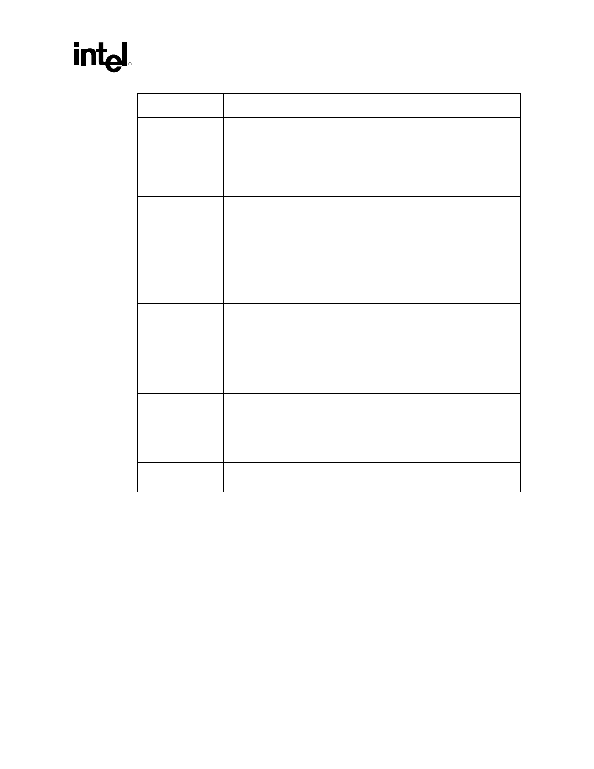
Revision History
Rev. No. Description Rev. Date
-001 • Initial Release. Sept 2001
-002 • Added Section 2.4, Electrostatic Discharge Platform
Recommendations
• Replaced Figure 98, Power Delivery Map, in Section 13, Power
Delivery
• Revised Section 13.4.3, 3.3V/V5REF Sequencing
• Revised Table 33. Intel
(3-DIMM) Clocks, in Section 12.2, 3-DIMM Clocking
• Revised Table 32, Intel
12.1, 2-DIMM Clocking
• Replaced Figure 79, RTC Power Well Isolation Control, in Section
11.8.6, Power Well Isolation Control Requirements
• Replaced Figure 84, Trace Routing, in Section 11.9.2.1, General
Trace Routing Considerations
• Revised Section 13.4.3, 3.3V/V5REF Sequencing
• Revised Checklist Recommendations for 5V_REF_SUS in
Section 14.4.15, Power
• Added SUSCLK to the RTC Checklist in Section 14.4.12
• Added Section 10.3 Power Supply PS_ON Considerations
®
CK-815 (3-DIMM) Clocks, Intel® CK-815
®
CK-815 (2-DIMM) Clocks, in Section
Aug 2002
R
®
12 Intel
815EG Chipset Platform Design Guide
Page 13

Introduction
R
1 Introduction
1.1 Design Guide and Chipset Basic Information
This design guide organizes Intel design recommendations for the Intel® 815EG chipset platform
for use with universal socket 370. In addition to providing motherboard design recommendations
(e.g., layout and routing guidelines), this document also addresses system design issues (e.g.,
thermal requirements) for the chipset platform.
This design guide contains design recommendations, debug recommendations, and a system
checklist. These design guidelines are developed to ensure maximum flexibility for board
designers while reducing the risk of board-related issues.
Consult the debug recommendations when debugging your design. However, these debug
recommendations should be understood before completing board design to ensure that the debug
port, in addition to other debug features, are implemented correctly.
There is no AGP port capability in the Intel
®
82815EG GMCH. The 82815EG uses internal
graphics only.
There are six chipsets in the Intel
®
• Intel
• Intel
• Intel
82815 chipset: This chipset contains the Intel 82815 and the Intel® 82801AA ICH.
®
82815E chipset: This chipset contains the Intel 82815E and the Intel® 82801BA ICH2.
®
82815P chipset: This chipset contains the Intel 82815P and the 82801AA ICH. There is
815 chipset family:
no internal graphics capability. This GMCH uses an AGP port only.
®
• Intel
82815EP chipset: This chipset contains the Intel 82815EP and the 82801BA ICH2.
There is no internal graphics capability. This GMCH uses an AGP port only.
®
• Intel
82815G chipset: This chipset contains the 82815G GMCH and 82801AA ICH. There is
no AGP port capability. This GMCH uses internal graphics only.
®
• Intel
82815EG chipset. This chipset contains the 82815EG GMCH and Intel 82801BA
ICH2. There is no AGP port capability. This GMCH uses internal graphics only.
The only component difference between the 82815 GMCH and the 82815E GMCH is the I/O
Controller Hub. The only component difference between the 82815P GMCH and the 82815EP
GMCH is the I/O Controller Hub. The only component difference between the 82815G GMCH
and the 82815EG GMCH is the I/O Controller Hub.
The Intel 815EG chipset platform supports the following processors:
®
• Intel
• Intel
Pentium® III processor based on 0.18 micron technology (CPUID = 068xh).
®
Celeron® processor based on 0.18 micron technology (CPUID = 068xh). This applies to
Celeron 533A MHz and ≥566 MHz processors
• Future 0.13 micron socket 370 processors
®
815EG Chipset Platform Design Guide 13
Intel
Page 14
Introduction
The system bus speed supported by the design is based on the capabilities of the processor,
chipset, and clock driver.
The 815 chipset for use with the universal socket 370 is not compatible with the
®
Intel
Pentium® II processor (CPUID = 066xh) 370-pin socket.
1.2 Terminology
This section describes some of the terms used in this document. Additional power delivery term
definitions are provided at the beginning of Chapter13, “Power Delivery”.
Term Description
AGP Accelerated Graphics Port
R
AGTL/AGTL+ Refers to processor bus signals that are implemented using either Assisted
Bus Agent A component or group of components that, when combined, represent a single load
Crosstalk The reception on a victim network of a signal imposed by aggressor network(s)
GMCH Graphics and Memory Controller Hub. A component of the Intel 815 chipset
ICH Intel 82801AA I/O Controller Hub component.
ISI Inter-symbol interference is the effect of a previous signal (or transition) on the
Gunning Transceiver Logic (AGTL+) or its lower voltage variant (AGTL), depending
on which processor is being used.
on the AGTL+ bus.
through inductive and capacitive coupling between the networks.
• Backward Crosstalk–coupling that creates a signal in a victim network that travels
in the opposite direction as the aggressor’s signal.
• Forward Crosstalk–coupling that creates a signal in a victim network that travels
in the same direction as the aggressor’s signal.
• Even Mode Crosstalk–coupling from single or multiple aggressors when all the
aggressors switch in the same direction that the victim is switching.
• Odd Mode Crosstalk–coupling from single or multiple aggressors when all the
aggressors switch in the opposite direction that the victim is switching.
platform for use with the Universal Socket 370
interconnect delay. For example, when a signal is transmitted down a line and the
reflections due to the transition have not completely dissipated, the following data
transition launched onto the bus is affected. ISI is dependent upon frequency, time
delay of the line, and the reflection coefficient at the driver and receiver. ISI can
impact both timing and signal integrity.
Network Length The distance between agent 0 pins and the agent pins at the far end of the bus.
Pad The electrical contact point of a semiconductor die to the package substrate. A pad
Pin The contact point of a component package to the traces on a substrate such as the
14 Intel
is only observable in simulation.
motherboard. Signal quality and timings can be measured at the pin.
®
815EG Chipset Platform Design Guide
Page 15
Introduction
R
Term Description
Ringback The voltage that a signal rings back to after achieving its maximum absolute value.
Ringback may be due to reflections, driver oscillations, or other transmission line
phenomena.
Setup Window The time between the beginning of Setup to Clock (T
) and the arrival of a
SU_MIN
valid clock edge. This window may be different for each type of bus agent in the
system.
SSO Simultaneous Switching Output (SSO) Effects refers to the difference in electrical
timing parameters and degradation in signal quality caused by multiple signal
outputs simultaneously switching voltage levels (e.g., high-to-low) in the opposite
direction from a single signal (e.g., low-to-high) or in the same direction (e.g., highto-low). These are respectively called odd-mode switching and even-mode
switching. This simultaneous switching of multiple outputs creates higher current
swings that may cause additional propagation delay (or “push-out”), or a decrease
in propagation delay (or “pull-in”). These SSO effects may impact the setup and/or
hold times and are not always taken into account by simulations. System timing
budgets should include margin for SSO effects.
Stub The branch from the bus trunk terminating at the pad of an agent.
System Bus The system bus is the processor bus.
Trunk The main connection, excluding interconnect branches, from one end agent pad to
the other end agent pad.
Undershoot Minimum voltage observed for a signal to extend below VSS at the device pad.
Universal Socket 370 Refers to the Intel 815EG chipset using the “universal” PGA370 socket. In general,
these designs support 66/100/133 MHz system bus operation, Intel
guidelines for future 0.13 micron processors, and Celeron
(CPUID=068xh), Pentium
®
III processor (CPUID=068xh), and future Celeron and
®
®
VRM
processors
Pentium III processors using 0.13 micron technology in single-microprocessor
based designs.
Victim A network that receives a coupled crosstalk signal from another network is called
the victim network.
®
815EG Chipset Platform Design Guide 15
Intel
Page 16
Introduction
1.3 Reference Documents
R
Document Document Number /
Intel® 815 Chipset Family: 82815G/82815EG Graphic s and Memory Controller
Hub (GMCH) for use with the Univ ersal Socket 370 Datasheet
Intel® 82802AB/82802AC Firmware Hub (FWH) Datasheet Doc 290658
Intel® 82801BA I/O Controller Hub (ICH2) and Intel® 82801BAM I/O Controller
Hub (ICH2-M) Datasheet
Intel® Pentium® III Processor Specification Update (latest revision from website) http://developer.intel.co
AP 907 Intel® Pentium® III Processor Power Distribution Guidelines Doc 245085
AP-585 Intel® Pentium® II Processor AGTL+ Guidelines Doc 243330
AP-587 Intel® Pentium® II Processor Power Distribution Guidelines Doc 243332
Accelerated Graphics P ort Interface Specification, Revision 2.0 http://www.intel.com/te
Graphics Performance Accel erator Specification ftp://download.intel.co
PCI Local Bus Specification, Revision 2. 2 http://www.pcisig.com/s
AC ’97 Component Specification, Revision 2.2
Communication Network Riser Specification, Revision 1.1 http://developer.intel.co
Universal Serial Bus, Revision 2.0 Specification http://www.usb.org/dev
(1)
http://developer.intel.co
Location
Doc 290714
Intel developer website
Intel developer website
Doc 290687
Intel developer website
m/design/PentiumIII/sp
ecupdt/
Intel developer website
Intel developer website
Intel developer website
chnology/agp/agp_inde
x.htm)
m/technology/agp/dow
nloads/agp20.pdf
pecifications/conventio
nal_pci
m/ial/scalableplatforms
/audio/index.htm
m/technology/cnr/
elopers/usb20/
NOTES:
1. Throughout this document, this specification will be referred to as AC ’97 v2.2.
®
16 Intel
815EG Chipset Platform Design Guide
Page 17

Introduction
R
1.4 System Overview
The 815EG chipset platform for use with the universal socket 370 contains a Graphics and
Memory Controller Hub (GMCH) component and I/O Controller Hub 2 (ICH2) component for
desktop platforms.
The GMCH provides the processor interface (optimized for future 0.13 micron Celeron processors
and Pentium III processors (socket 370) and the Pentium III processors (CPUID = 068xh), DRAM
interface, hub interface, and internal graphics. It does not provide support for an external AGP
port. This product provides flexibility and scalability in memory subsystem performance. PC100
SDRAM system memory may be scaled to PC133 system memory.
The Accelerated Hub Architecture interface (i.e., the chipset component interconnect) is designed
into the chipset to provide an efficient, high-bandwidth communication channel between the
GMCH and the I/O controller hub. The chipset architecture also enables a security and
manageability infrastructure through the Firmware Hub component.
An ACPI-compliant 815EG chipset platform can support the Full-on (S0), Stop Grant (S1),
Suspend to RAM (S3), Suspend to Disk (S4), and Soft-off (S5) power management states. The
chipset also supports wake-on-LAN for remote administration and troubleshooting. The chipset
architecture removes the requirement for the ISA expansion bus that was traditionally integrated
into the I/O subsystem of PCIsets/AGPsets. This removes many of the conflicts experienced when
installing hardware and drivers into legacy ISA systems. The elimination of ISA provides true
plug-and-play for the platform. Traditionally, the ISA interface was used for audio and modem
devices. The addition of AC ’97 allows the OEM to use software-configurable AC ’97 audio and
modem coder/decoders (codecs), instead of the traditional ISA devices.
®
815EG Chipset Platform Design Guide 17
Intel
Page 18
Introduction
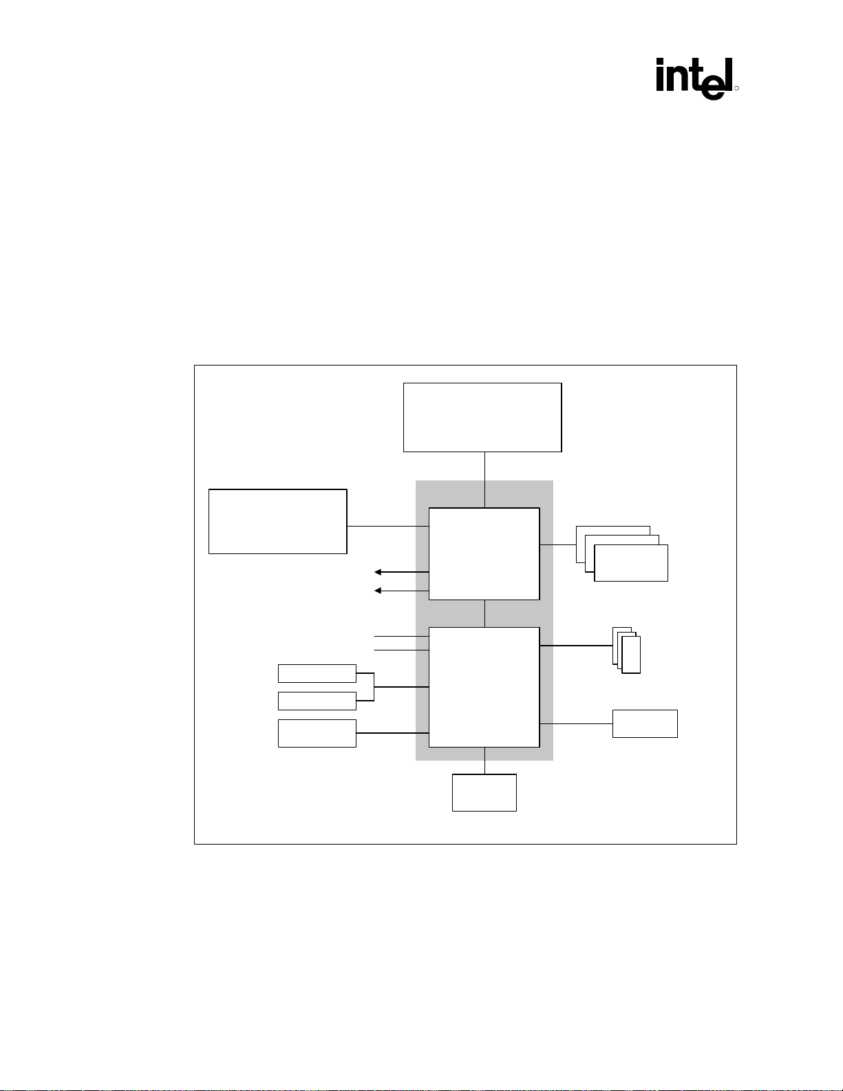
1.4.1 System Features
The 815EG chipset platform contains two components: the 82815EG Graphics and Memory
Controller Hub (GMCH) and the 82801BA I/O Controller Hub 2 (ICH2). The GMCH integrates a
66/100/133 MHz, P6 family system bus controller, integrated 2D/3D graphics accelerator,
100/133 MHz SDRAM controller, and a high-speed accelerated hub architecture interface for
communication with the ICH2. The ICH2 integrates an UltraATA/100 controller, 2 Universal
Serial Bus (USB) host controllers with a total of 4 ports, Low Pin Count (LPC) interface
controller, Firmware Hub (FWH) interface controller, PCI interface controller, AC-link, integrated
LAN controller, and a hub interface for communication with the GMCH.
Figure 1. System Block Diagram
Intel Celeron and Pentium III
Processors Using 0.13 Micron
Technology
R
Display Cache
AIMM
(AGP in-line memory module)
Analog display out
Digital video out
Audio codec
Modem codec
LAN connect
component
4x USB
2x IDE
AC97
LAN
connect
815EG
Chipset
82815EG B-0
GMCH
82801BA ICH2
FWH
Flash BIOS
66/100/133 MHz system bus
Hub interface
PCI bus
LPC I/F
Sys_Blk_815E_B0
100/133 MHz
SDRAM
PCI slots
KBC/SIO
®
18 Intel
815EG Chipset Platform Design Guide
Page 19
Introduction
R
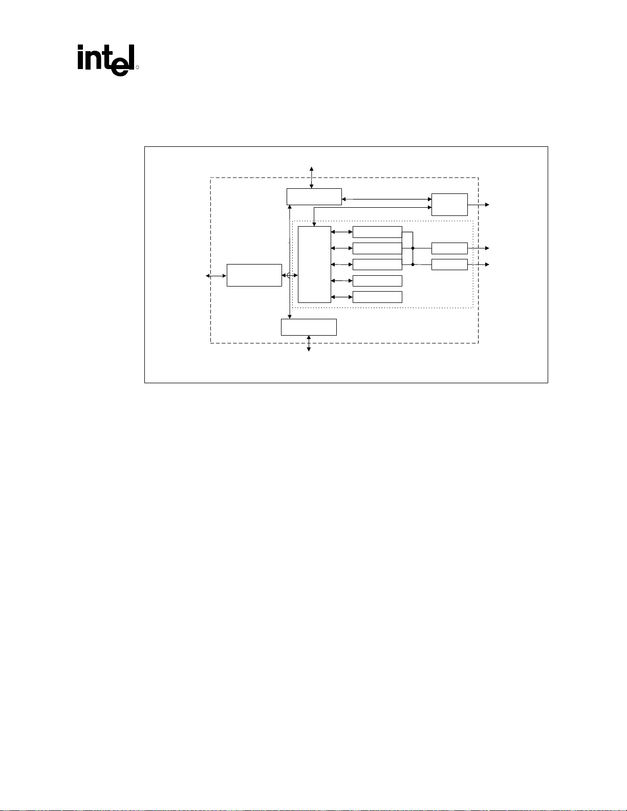
1.4.2 Component Features
Figure 2. Component Block Diagram
System bus (66/100/133 MHz)
Processor I/F
Data
stream
GPA or AIMM
Card
Local memory I/F
control &
dispatch
Hub I/F
Hub
1.4.2.1 Intel® 82815EG GMCH Features
• Processor/System Bus Support
Optimized for Celeron and Pentium III processors which use 0.13 micron technology at
133 MHz system bus frequency
Support for Celeron and Pentium III processors (CPUID = 068xh); at 66 MHz system bus
frequency
Supports 32-bit AGTL or AGTL+ bus addressing
Supports uniprocessor systems
Utilizes AGTL and AGTL+ bus driver technology (gated AGTL/AGTL+ receivers for
reduced power)
Primary display
Overlay
H/W cursor
3D pipeline
2D (blit engine)
System
memory I/F
RAMDAC
FP / TVout
Internal graphics
comp_blk_1
SDRAM
100/133
MHz, 64 bit
Monitor
Digital
video out
• Integrated DRAM controller
32 MB to 512 MB using 16-Mb/64-Mb/128-Mb technology
Supports up to three double-sided DIMMS (6 rows)
100 MHz, 133 MHz SDRAM interface
64-bit data interface
Standard Synchronous DRAM (SDRAM) support (x-1-1-1 access)
Supports only 3.3 V DIMM DRAM configurations
No registered DIMM support
Support for symmetrical and asymmetrical DRAM addressing
Support for x8, x16 DRAM device widths
Refresh mechanism: CAS-before-RAS only
Support for DIMM serial PD (presence detect) scheme via SMbus interface
Suspend-To-RAM (STR) power management support via self-refresh mode using CKE
®
815EG Chipset Platform Design Guide 19
Intel
Page 20
Introduction
• Integrated Graphics Controller
Full 2D/3D/DirectX acceleration
Texture-mapped 3D with point sampled, bilinear, trilinear, and anisotropic filtering
Hardware setup with support for strips and fans
Hardware motion compensation assist for software MPEG/DVD decode
Digital Video Out interface for support of digital displays and TV-Out
PC99A/PC2001 compliant
Integrated 230 MHz DAC
• Integrated Local Graphics Memory Controller (Display Cache)
0 MB to 4 MB (via Graphics Performance Accelerator) using zero, one or two parts
32-bit data interface
133 MHz memory clock
Supports only 3.3 V SDRAMs
• Packaging/Power
544-ball mBGA CSP with local memory port
1.85 V core and mixed 3.3 V, 1.5 V, and AGTL+ IO. Note that the 82801BA ICH2 has a
1.8 V requirement and the 82815EG GMCH has a 1.85 V requirement. Instead of using
separate voltage regulators to meet these requirements, a single voltage regulator can be
set to 1.795 V to 1.910 V. See Figure 98. Power Delivery Map.
R
1.4.2.2 Intel® 815 to 815G/EG Signal Name Changes
Intel 82815G/EG pins associated with AGP signals have name changes. The following table shows
the old Intel 82815 signal name, the ball number, and the new Intel 82815G/EG signal name. New
designs for new 815G/EG boards should use pull-ups or pull-downs as indicated by the 815G/EG
signal name. 815 boards using 815GEG devices may leave the associated 815 pins in the original
815 configuration.
Table 1. Intel
NOTES:
®
82815 to Intel® 82815G Pin Name Changes
Intel® 815 Signal
Name
WBF# AB24 PU
AD_STB0 M22 PD
AD_STB0# L23 PU
AD_STB1 U22 PD
AD_STB1# V23 PU
SB_STB Y23 PD
SB_STB# AA24 PU
GRCOMP J26 PD40
AGPREF J24 0.5VDDQ
G_GNT# AD25 NC
G_AD[24] V25 PD
NC = No Connect. These pins should float
PU = Pull-up to 3.3 V through a weak pull-up resistor. (8.2 kΩ to 10 kΩ resistor.)
PD = Pull-down. These pins should be pulled down to ground through a weak pull- down resistor.
(8.2 kΩ to 10 kΩ resistor.)
PD40 = Pull-down to VSS using a 40 resistor.
0.5VDDQ = Set to 50% of the VDDQ voltage supply level.
Ball# Intel® 815G/EG
Signal Name
®
20 Intel
815EG Chipset Platform Design Guide
Page 21

Introduction
R
1.4.2.3 Intel® 82801BA I/O Controller Hub 2 (ICH2)
The Intel® I/O Controller Hub 2 allows the I/O subsystem to access the rest of the system, as
follows:
• Upstream accelerated hub architecture interface for access to the GMCH
• PCI 2.2 interface (6 PCI Request/Grant pairs)
• 2 channel Ultra ATA/100 Bus Master IDE controller
• USB controller (Expanded capabilities for 4 ports)
• I/O APIC
• SMBus controller
• FWH interface
• LPC interface
• AC ’97 Component Specification, Revision 2.2 interface
• Integrated system management controller
• Alert-on-LAN*
• Integrated LAN controller
• Packaging/Power
360 EBGA
1.8 V (± 3% within margins of 1.795 V to 1.9 V) core and 3.3 V standby
1.4.2.4 Firmware Hub (FWH)
The hardware features of the firmware hub include:
• An integrated hardware Random Number Generator (RNG)
• Register-based locking
• Hardware-based locking
• Five General Purpose Interrupts (GPI)
• Packaging/Power
40L TSOP and 32L PLCC
3.3 V core and 3.3 V / 12V for fast programming
1.4.3 Platform Initiatives
1.4.3.1 Universal Motherboard Design
The 815EG chipset platform for use with the universal socket 370 allows systems designers to
build one system that is compatible with the Pentium III processor (CPUID=068xh), Celeron
processor (CPUID=068xh), and future 0.13 micron socket 370 processors. When implemented,
the 815EG chipset universal socket 370 platform can detect which processor is present in the
socket and function accordingly.
®
815EG Chipset Platform Design Guide 21
Intel
Page 22

Introduction
1.4.3.2 Intel® PC 133
The PC133 initiative provides the memory bandwidth necessary to obtain high performance from
the processor and AGP graphics controller. The platform’s SDRAM interface supports 100 MHz
and 133 MHz operation. The latter delivers 1.066 GB/s of theoretical memory bandwidth
compared with the 800 MB/s theoretical memory bandwidth of 100 MHz SDRAM systems.
1.4.3.3 Accelerated Hub Architecture Interface
As I/O speeds increase, the demand placed on the PCI bus by the I/O bridge becomes significant.
With the addition of AC ’97 and Ultra ATA/100, coupled with the existing USB, I/O requirements
could impact PCI bus performance. The 815EG platform’s accelerated hub architecture ensures
that the I/O subsystem, both PCI and the integrated I/O features (IDE, AC ’97, USB, LAN),
receives adequate bandwidth. By placing the I/O bridge on the accelerated hub architecture
interface instead of PCI, I/O functions integrated into the ICH2 and the PCI peripherals are
ensured the bandwidth necessary for peak performance.
1.4.3.4 Internet Streaming SIMD Extensions
R
The Pentium III processors provide 70 new SIMD (single instruction, multiple data) instructions.
The new extensions are floating-point SIMD extensions. Intel
integer SIMD instructions. The Internet Streaming SIMD extensions complement the MMX
technology SIMD instructions and provide a performance boost to floating-point-intensive 3D
applications.
1.4.3.5 Integrated LAN Controller
The 815EG chipset platform incorporates an ICH2 integrated LAN Controller. Its bus master
capabilities enable the component to process high-level commands and perform multiple
operations; this lowers processor utilization by off-loading communication tasks from the
processor.
The ICH2 functions with several options of LAN connect components to target the desired market
segment. The 82562EH provides a HomePNA 1 Mbit/sec connection. The 82562ET provides a
basic Ethernet 10/100 connection. The 82562EM provides an Ethernet 10/100 connection with the
added flexibility of Alert on LAN. More advanced LAN solutions can be implemented with the
82550 or other PCI based product offerings.
1.4.3.6 Ultra ATA/100 Support
The 815EG chipset platform incorporates an IDE controller with two sets of interface signals
(primary and secondary) that can be independently enabled, tri-stated or driven low. The
component supports Ultra ATA/100, Ultra ATA/66, Ultra ATA/33, and multiword PIO modes for
transfers up to 100 MB/sec.
®
MMX™ technology provides
1.4.3.7 Expanded USB Support
The 815EG chipset platform contains two USB Host Controllers. Each Host Controller includes a
root hub with two separate USB ports each, for a total of 4 USB ports. The addition of a second
USB Host Controller expands the functionality of the platform.
®
22 Intel
815EG Chipset Platform Design Guide
Page 23

Introduction
R
1.4.3.8 Manageability and Other Enhancements
The 815EG chipset platform integrates several functions designed to manage the system and lower
the total cost of ownership (TCO) of the system. These system management functions are designed
to report errors, diagnose the system, and recover from system lockups, without the aid of an
external microcontroller.
SMBus
The ICH2 integrates an SMBus controller. The SMBus provides an interface for managing
peripherals such as serial presence detection (SPD) and thermal sensors. The slave interface allows
an external microcontroller to access system resources.
Interrupt Controller
The interrupt capabilities of the platform expand support for up to 8 PCI interrupt pins and
PCI 2.2 message-based interrupts. In addition, the ICH2 supports system bus interrupt delivery.
Firmware Hub (FWH)
The platform supports firmware hub BIOS memory sizes up to 8 MB for increased system
flexibility.
1.4.3.9 AC ’97 6-Channel Support
The AC ’97 v2.2 defines a digital interface that can be used to attach an audio codec (AC), a
modem codec (MC), an audio/modem codec (AMC), or both an AC and an MC. The AC ’97 v2.2
defines the interface between the system logic and the audio or modem codec known as the “AClink.”
The 815EG chipset platform’s AC ’97 (with the appropriate codecs) not only replaces ISA audio
and modem functionality, but also improves overall platform integration by incorporating the AClink. Using the platform’s integrated AC-link reduces cost and eases migration from ISA.
By using an audio codec, the AC-link allows for cost-effective, high-quality, integrated audio. In
addition, an AC ’97 soft modem can be implemented with the use of a modem codec. Several
system options exist when implementing AC ’97. The 815EG chipset platform’s integrated digital
link allows several external codecs to be connected to the ICH2. The system designer can provide
audio with an audio codec, a modem with a modem codec, or an integrated audio/modem codec
(Figure 3c). The digital link is expanded to support two audio codecs (Figure 3a) or a combination
of an audio and modem codec (Figure 3b).
®
815EG Chipset Platform Design Guide 23
Intel
Page 24

Introduction
Modem implementation for different countries must be taken into consideration, as telephone
systems may vary. By implementing a split design, the audio codec can be on board, and the
modem codec can be placed on a riser. is developing an AC-link connector. With a single
integrated codec, or AMC, both audio and modem can be routed to a connector near the rear panel
where the external ports can be located.
The digital link in the ICH2 is AC ’97 v2.2 compliant, supporting two codecs with independent
PCI functions for audio and modem. Microphone input and left and right audio channels are
supported for a high-quality, two-speaker audio solution. Wake-on-ring-from-suspend also is
supported with the appropriate modem codec.
The 815EG chipset platform expands audio capability with support for up to six channels of PCM
audio output (i.e., full AC3 decode). Six-channel audio consists of Front Left, Front Right, Back
Left, Back Right, Center and Woofer, for a complete surround sound effect. ICH2 has expanded
support for two audio codecs on the AC-link.
R
®
24 Intel
815EG Chipset Platform Design Guide
Page 25
Introduction
®
®
R
Figure 3. AC ’97 Audio and Modem Connections
a) AC'97 with Audio C odecs ( 4-Channel Secondary)
AC’97
Audio
Codec
ICH2
Intel
360 EBGA
AC-link
AC’97
Audio
Codec
Audio Port
Audio Port
b) AC'97 with Modem and Audio Codecs
Intel® ICH2
360 EBGA
c) AC'97 with Audio/Modem Codec
ICH2
Intel
360 EBGA
AC-link
AC-link
Modem Port
AC’97
Modem
Codec
AC’97
Audio
Codec
Audio Port
Modem Port
AC’97
Audio/
Modem
Codec
Audio Port
®
815EG Chipset Platform Design Guide 25
Intel
Page 26

Introduction
1.4.3.10 Low-Pin-Count (LPC) Interface
In the 815EG chipset platform, the Super I/O (SIO) component has migrated to the Low-PinCount (LPC) interface. Migration to the LPC interface allows for lower-cost Super I/O designs.
The LPC Super I/O component requires the same feature set as traditional Super I/O components.
It should include a keyboard and mouse controller, floppy disk controller, and serial and parallel
ports. In addition to the Super I/O features, an integrated game port is recommended because the
AC ’97 interface does not provide support for a game port. In systems with ISA audio, the game
port typically existed on the audio card. The fifteen-pin game port connector provides for two
joysticks and a two-wire MPU-401 MIDI interface. Consult your preferred Super I/O vendor for a
comprehensive list of the devices offered and the features supported.
In addition, depending on system requirements, specific system I/O requirements may be
integrated into the LPC Super I/O. For example, a USB hub may be integrated to connect to the
ICH2 USB output and extend it to multiple USB connectors. Other SIO integration targets include
a device bay controller or an ISA-IRQ-to-serial-IRQ converter to support a PCI-to-ISA bridge.
Contact your Super I/O vendor to ensure the availability of desired LPC Super I/O features.
R
®
26 Intel
815EG Chipset Platform Design Guide
Page 27
General Design Considerations
R
2 General Design Considerations
This design guide provides motherboard layout and routing guidelines for systems based on the
815EG chipset for use with the universal socket 370. The document does not discuss the functional
aspects of any bus or the layout guidelines for an add-in device.
If the guidelines listed in this document are not followed, it is very important that thorough signal
integrity and timing simulations be completed for each design. Even when the guidelines are
followed, critical signals should be simulated to ensure the proper signal integrity and flight time.
As bus speeds increase, it is imperative that the guidelines documented are followed precisely.
Any deviation from these guidelines should be simulated.
The trace impedance typically noted (i.e., 60 Ω ± 15%) is the “nominal” trace impedance for a
5 mil-wide trace. That is, it is the impedance of the trace when not subjected to the fields created
by changing current in neighboring traces. When calculating flight times, it is important to
consider the minimum and maximum impedance of a trace, based on the switching of neighboring
traces. The use of wider spaces between the traces can minimize this trace-to-trace coupling. In
addition, these wider spaces reduce crosstalk and settling time.
Coupling between two traces is a function of the coupled length, the distance separating the traces,
the signal edge rate, and the degree of mutual capacitance and inductance. To minimize the effects
of trace-to-trace coupling, follow the routing guidelines documented in this section.
The routing guidelines in this design guide have been created using a PCB stack-up similar to that
shown in Figure 4. If this stack-up is not used, extremely thorough simulations of every interface
must be completed. Using a thicker dielectric (prepreg) will make routing very difficult or
impossible.
2.1 Nominal Board Stack-Up
The 815EG chipset platform requires a board stack-up yielding a target impedance of 60 Ω ± 15%
with a 5-mil nominal trace width. Figure 4 shows an example stack-up that achieves this. It is a 4layer printed circuit board (PCB) construction using 53%-resin FR4 material.
Figure 4. Board Construction Example for 60 ΩΩΩΩ Nominal Stack-up
Component-side layer 1: ½ oz. Cu
4.5-mil prepreg
Power plane layer 2: 1 oz. Cu
~48-mil core
Ground layer 3: 1 oz. Cu
4.5-mil prepreg
Solder-side layer 4: ½ oz. Cu
Total thickness:
62 mils
board_4.5mil_stackup
®
815EG Chipset Platform Design Guide 27
Intel
Page 28

General Design Considerations
2.2 Future Designs Require Pull-Ups and Pull-Downs on Any Unused Input and I/O Pins
Any new 815EG platform Universal Socket 370 design should insure no input or I/O pin is left
floating. For example, the TVCLKIN/INT# pin on many current 815 designs is left floating. This
pin should be pulled up to 1.8 V by a weak pull-up resistor (8.2 kΩ to 10 kΩ) on any future
815EG Universal Socket 370 design.
2.3 Support For P-MOS Kicker “ON”: SMAA[9] Is
Strapped High by an Internal 50 kΩΩΩΩ Pull-Up Resistor
The PSB P-MOS Kicker circuit should be enabled on all new, future 82815EG Universal Socket
370 designs. Use of the P-MOS Kicker circuit improves PSB timings by improving AGTL and
AGTL+ signal flight time. The 82815EG SMAA[9] is strapped high through an internal 50 kΩ
pull-up resistor to enable the PSB P-MOS Kicker.
Existing 815 designs which have implemented the pull-down resistor circuit on the SMAA[9]
signal as shown in the 815 Customer Reference Board schematics and populated the resistor site to
over-ride the internal pull-up resistor, may depopulate the site to enable the P-MOS Kicker circuit.
This activity should be based on timing analysis of the specific platform.
R
P-MOS Kicker circuit “ON” is the recommended setting for 82815EG Universal Socket 370
designs using future 0.13 micron technology processors.
2.4 Electrostatic Discharge Platform Recommendations
Electrostatic discharge (ESD) into a system can lead to system instability, and possibly cause
functional failures when a system is in use. There are system level design methodologies that when
followed can lead to higher ESD immunity. Electromagnetic fields due to ESD are introduced into
a system through chassis openings such as the I/O back panel and PCI slots. These fields can
introduce noise into signals and cause the system to malfunction. One can reduce the potential for
issues at the I/O area by adding more ground plane on the motherboard around the I/O area. This
can lead to a higher ESD immunity.
Intel recommends that the I/O area on the top and bottom signal layers of a 4-layer motherboard
near the I/O back panel be filled with a ground fill as shown in Figures 1-4. In addition, a ground
fill cutout should be placed on the Vcc layer in the area where the ground fill is done on the top
and bottom layers. Intel recommends filling the I/O area as much as possible without effecting the
signal routing. The board designer should fill the entire I/O area along the board edge.
The spacing from the ground fill to other shapes/traces should be at least 20 mils. It is
recommended that these ground fill areas be connected to two chassis mounting holes (as seen in
Figure 2). This will allow ESD current to travel to the chassis instead of the board. Ground
stitching vias should be placed throughout the entire ground fill if possible. It is important that the
vias are placed along the board edge. Ground stitching vias for the ground fill should be 100-150
mils apart or less.
In conclusion, Intel recommends the following:
®
28 Intel
815EG Chipset Platform Design Guide
Page 29
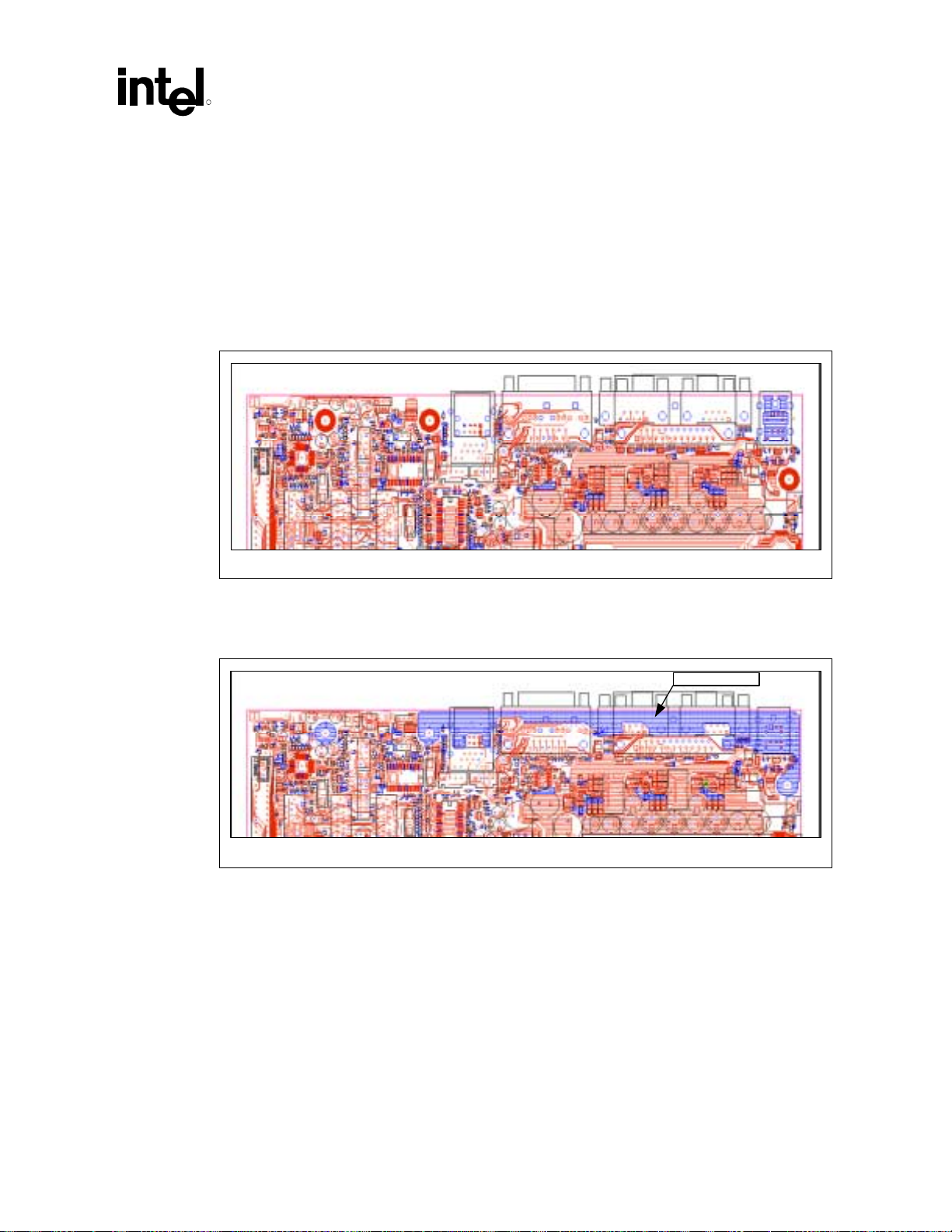
General Design Considerations
R
• 1. Fill the I/O area with the ground fill in all layers including signal layers whenever possible
• 2. Extend the ground fill along the entire back I/O area
• 3. Connect the ground fill to mounting holes
4. Place stitching vias 100-150 mils apart in the entire ground fill
Figure 5. Top Signal Layer before the Ground Fill Near the I/O Layer
Figure 6. Top Signal Layer after the Ground Fill Near the I/O Layer
Ground Fill
®
815EG Chipset Platform Design Guide 29
Intel
Page 30
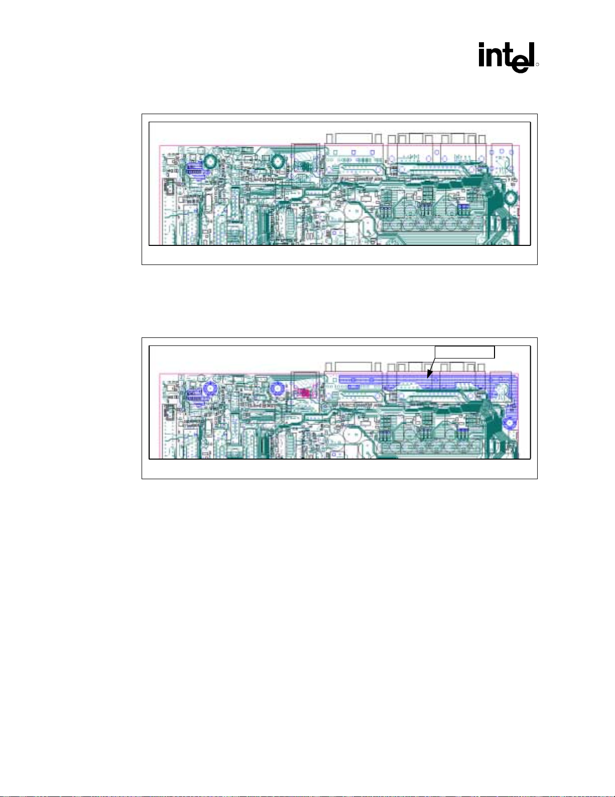
General Design Considerations
Figure 7. Bottom Signal Layer before the Ground Fill Near the I/O Area
Figure 8. Bottom Signal Layer after the Ground Fill Near the I/O
R
Ground Fill
®
30 Intel
815EG Chipset Platform Design Guide
Page 31

Component Layouts
R
3 Component Layouts
Figure 9 illustrates the relative signal quadrant locations on the GMCH ballout. It does not
represent the actual ballout. Refer to the Intel
®
82815 Chipset Family: 82815G/82815EG
Graphics and Memory Controller Hub (GMCH) for use with the Universal Socket 370 Datasheet
for the actual ballout.
Figure 9. GMCH 544-Ball µµµµBGA* CSP Quadrant Layout (Top View)
Pin 1
corner
System Memory
GMCH
Hub Interface
AGP /
Display Cache
System Bus
Video
Quad_GM CH
®
815EG Chipset Platform Design Guide 31
Intel
Page 32

Component Layouts
R
Figure 10 illustrates the relative signal quadrant locations on the ICH2 ballout. It does not
represent the actual ballout. Refer to the Intel
®
82801BA I/O Controller Hub (ICH2) and Intel®
82801BAM I/O Controller Hub (ICH2-M) Datasheet for the actual ballout.
Figure 10. ICH2 360-Ball EBGA Quadrant Layout (Top View)
Hub interface Processor
LAN
ICH2
IDE
SM bus
AC'97
PCI LPC USB
Quad_ICH2
®
32 Intel
815EG Chipset Platform Design Guide
Page 33

Component Layouts
R
Figure 11. Firmware Hub (FWH) Packages
1234 323130
1
2
3
4
5
6
7
8
9
10
11
12
13
14
15
16
17
18
19
20
FWH Interface
(40-Lead TSOP)
40
39
38
37
36
35
34
33
32
31
30
29
28
27
26
25
24
23
22
21
5
6
7
8
9
10
11
12
13
14 15 16 17 18 19 20
FWH Interface
(32-Lead PLCC,
0.450" x 0.550")
Top View
29
28
27
26
25
24
23
22
21
pck_fwh.vsd
®
815EG Chipset Platform Design Guide 33
Intel
Page 34

Component Layouts
This page is intentionally left blank.
R
®
34 Intel
815EG Chipset Platform Design Guide
Page 35

Universal Socket 370 Design
R
4 Universal Socket 370 Design
4.1 Universal Socket 370 Definitions
The universal socket 370 platform supports Pentium III processor (CPUID=068xh) and Celeron
processor (CPUID=068xh) as well as future 0.13 micron socket 370 processors. The Pentium III
processor (CPUID=068xh) and Celeron processor (CPUID=068xh) have different requirements
for functioning properly in a platform than the future 0.13 micron socket 370 processors. It is
necessary to understand these differences and how they affect the design of the platform. Refer to
Table 2 through Table 5 for a high-level description of the differences that require additional
circuitry on the motherboard. Specific details on implementing this circuitry are discussed further
in this chapter. For a detailed description of the differences between the Pentium III processor
(CPUID=068xh) / Celeron processor (CPUID=068xh), and future 0.13 micron socket 370
processor pins, refer to Section 5.4.
Table 2. Processor Considerations for Universal Socket 370 Design
Signal
Name or
Pin
Number
AF36 VSS DETECT Addition of circuitry that generates
AG1 VSS VTT Addition of FET switch to ground
AJ3 VSS RESET2# Addition of stuffing option for pull-
AK22 GTL_REF VCMOS_REF Addition of resistor-divider network
Function In
®
Pentium® III
Intel
Processor
(CPUID=068xh) and
®
Intel
Celeron®
Processor
(CPUID=068xh)
Function In Future
0.13 Micron
Socket 370
Processors
Implementation for
Universal Socket 370 Design
a processor identification signal
used to configure board-level
operation.
or VTT, controlled by processor
identification signal.
Note: FET must have no more
than 100 milliohms
resistance between source
and drain.
down to ground, which lets
designer prevent future 0.13
micron socket 370 processors
from being used with incompatible
stepping of Intel 82815EG GMCH.
to provide 1.0 V, which will satisfy
voltage tolerance requirements of
the Pentium
(CPUID=068xh) and Celeron
processor (CPUID=068xh) as well
as future 0.13 micron socket 370
processors.
®
III processor
®
®
815EG Chipset Platform Design Guide 35
Intel
Page 36

Universal Socket 370 Design
R
Signal
Name or
Pin
Number
Function In
®
Pentium® III
Intel
Processor
(CPUID=068xh) and
®
Intel
Celeron®
Function In Future
0.13 Micron
Socket 370
Processors
Implementation for
Universal Socket 370 Design
Processor
(CPUID=068xh)
PICCLK Requires 2.5 V Requires 2.0 V Addition of FET switch to provide
proper voltage, controlled by
processor identification signal.
PWRGOOD Requires 2.5 V Requires 1.8 V Addition of resistor-divider network
to provide 2.1V, which will satisfy
voltage tolerance requirements of
the Pentium
III processor
(CPUID=068xh) and Celeron
processor (CPUID=068xh) as well
as future 0.13 micron socket 370
processors.
VTT Requires 1.5 V Requires 1.25 V Modification to VTT generation
circuit to switch between 1.5 V or
1.25 V, controlled by processor
identification signal.
VTTPWRGD Not used Input signal to future
0.13 micron socket 370
Addition of VTTPWRGD
generation circuit.
processors to indicate
that VID signals are
stable
Table 3. GMCH Considerations for Universal Socket 370 Design
Pin
Name/Number
SMAA[12] New strap required for determining
Pentium
(CPUID=068xh) and Celeron
Processor (CPUID=068xh)
or
Future 0.13 micron socket 370
processors
Issue Implementation For
Universal Socket 370 Design
Addition of FET switch controlled by
®
III Processor
®
processor identification signal.
Table 4. Intel® ICH2 Considerations for Universal Socket 370 Design
Signal Issue Implementation For Universal
PWROK GMCH and Intel CK-815 must not
sample BSEL[1:0] until VTTPWRGD
is asserted. The ICH2 must not
initialize before the Intel CK-815
clocks stabilize.
Addition of circuitry to have VTTPWRGD
gate PWROK from power supply to ICH2.
The ICH2 will hold the GMCH in reset until
VTTPWRGD asserted plus 20 ms time
delay to allow Intel CK-815 clocks to
stabilize.
Motherboard Design
®
36 Intel
815EG Chipset Platform Design Guide
Page 37

Universal Socket 370 Design
R
Table 5. Clock Synthesizer Considerations for Universal Socket 370 Design
Signal Issue Implementation For Universal
VDD Intel CK-815 does not support
VTTPWRGD
Addition of FET switch that supplies power
to VDD only when VTTPWRGD is
asserted.
Note: FET must have no more than 100
Motherboard Design
milliohms resistance between source
and drain.
4.2 Processor Design Requirements
4.2.1 Use of Universal Socket 370 Design w i th Incompatible GMCH
The universal socket 370 design is intended for use with the 815EG chipset platform for use with
the universal socket 370. A universal socket 370 design populated with an earlier stepping of the
GMCH is not compatible with future 0.13 micron socket 370 processors and, if used, will cause
eventual failure of these processors. To prevent a future 0.13 micron socket 370 processor from
being used with an incompatible stepping of the GMCH, the recommendation is to lay out the site
for a 0 Ω pull-down to ground on processor pin AJ3. This pin is a RESET# signal on future 0.13
micron socket 370 processors and, by populating the resistor, these future processors will be
prevented from functioning when placed in a board with an incompatible stepping of the GMCH.
All Pentium III (CPUID=068xh) and Celeron (CPUID=068xh) processors will continue to boot
normally. Not populating the resistor will allow future 0.13 micron socket 370 processors to boot.
Refer to Figure 12 for an example implementation.
Figure 12. Future 0.13 Micron Socket 370 Processor Safeguard for Universal Socket 370
Designs Using A-2 GMCH
Future 0.13 Micron
Socket 370
Processors
AJ3
Ω
0
Tual_pin_aj3
®
815EG Chipset Platform Design Guide 37
Intel
Page 38

Universal Socket 370 Design
4.2.2 Identifying the Processor at the Socket
For the platform to configure for the requirements of the processor in the socket, it must first
identify whether the processor is a Pentium III processor (CPUID=068xh) / Celeron processor
(CPUID=068xh), or a future 0.13 micron socket 370 processors. Pin AF36 is a ground pin on a
Pentium III processor (CPUID=068xh) and Celeron processor (CPUID=068xh); pin AF36 is a
detect pin on future 0.13 micron Socket 370 processors. Referring to Figure 13, the platform uses
a detect circuit connected to this processor pin. If a future 0.13 micron Socket 370 processor is
present in the socket, the TUAL5 reference schematic signal will be pulled to the 5 V rail and the
TUAL5# reference schematic signal will be pulled to ground. Otherwise, for a Pentium III
processor (CPUID=068xh) or Celeron processor (CPUID=068xh), the TUAL5 reference
schematic signal will be pulled to ground and the TUAL5# will be pulled to the 5 V rail.
Figure 13. Processor Detect Mechanism at Socket/TUAL5 Generation Circuit
VCC5
R
Processor Pin
AF36
1 KΩ
VTT
VCC5
2.2 KΩ
NPN
2.2 KΩ
MOSFET N
TUAL5#
Proc_Detect_815E_B0
TUAL5
®
38 Intel
815EG Chipset Platform Design Guide
Page 39

Universal Socket 370 Design
R
4.2.3 Setting the Appropriate Processor VTT Level
Because the Pentium III processor (CPUID=068xh) / Celeron processor (CPUID=068xh), and
future 0.13 micron socket 370 processors require different VTT levels, the platform must be able
to provide the appropriate voltage level after determining which processor is in the socket.
Referring to Figure 14, the TUAL5 reference schematic signal serves to control the FET, and by
doing so determines whether the voltage regulator supplies 1.25 V or 1.5 V to VTT for AGTL or
AGTL+, respectively.
Figure 14. V
TT Selection Switch
VCC3_3
LT1587-ADJ
Vin
10
µF
TUAL5
Vout
ADJ
0.1
µF
MOSFET N
49.9
1%
10
1%
Ω
Ω
µF
22
Tantalum
Vtt_Sel_Sw_815E_B0
VTT
®
815EG Chipset Platform Design Guide 39
Intel
Page 40

Universal Socket 370 Design
4.2.4 VTT Processor Pin AG1
Processor pin AG1 requires additional attention since it is a ground pin on a Pentium III processor
(CPUID=068xh) / Celeron processor (CPUID=068xh) and a VTT pin on a future 0.13 micron
socket 370 processor. A separate switch controlled by the TUAL5 reference schematic signal
determines whether pin AG1 is pulled to ground or VTT. Refer to Figure 15 for an example
implementation.
Figure 15. Switching Pin AG1
VTT
R
TUAL5
Note: The FET must have no more than
100 milliohms resistance between the
source and the drain.
Processor Pin
AG1
1 KΩ
AG1_Switch_815E_B0
®
40 Intel
815EG Chipset Platform Design Guide
Page 41

Universal Socket 370 Design
R
4.2.5 Identifying the Processor at the GMCH
The GMCH determines whether the socket contains a future 0.13 micron socket 370 processor or
Pentium III processor (CPUID=068xh) / Celeron processor (CPUID=068xh) based on the input to
pin SMAA12 on the GMCH. In a system using future 0.13 micron socket 370 processors,
SMAA12 will be pulled down during reset to indicate to the GMCH that a future 0.13 micron
socket 370 processor is in the socket. Refer to Figure 16. for an implementation example.
Figure 16. Processor Identification Strap on GMCH
SMAA[12]
10 KΩ
TUAL5
Proc_ID_Strap_815E_B0
Table 6 provides the logic decoding to determine which processor is installed in a PGA370 design.
Table 6. Determining the Installed Processor via Hardware Mechanisms
Processor Pin
AF36
Hi-Z 0 Future 0.13 micron socket 370 processor
Low 0 Pentium® III processor (CPUID=068xh) or
X 1 No processor installed.
CPUPRES# Notes
installed.
®
Celeron
processor (CPUID=068xh) installed.
®
815EG Chipset Platform Design Guide 41
Intel
Page 42

Universal Socket 370 Design
4.2.6 Configuring Non-VTT Processor Pins
When asserted, the VTTPWGRD signal must be level-shifted to 12V to properly drive the gating
circuitry of the CK-815. Furthermore, while the VTTPWRGD signal is connected to the
VTTPWRGD pin on a future 0.13 micron socket 370 processor, on a Pentium III processor
(CPUID=068xh) or Celeron processor (CPUID=068xh) that same pin is a ground. To provide
proper functionality, a 1.0 kΩ resistor must be placed in series between the circuitry that generates
the signal VTTPWRGD and the processor pin VTTPWRGD. Refer to Figure 17 for an example
implementation. Voltage regulators that generate the standard VTTPWRGD signal are available.
Figure 17. VTTPWRGD Configuration Circuit
VCC5
2.2 K
VCC12
Ω
R
VTTPWRGD12
1 KΩ
MOSFET N
VTTPWRGD5#
VTT
VTTPWRGD
1 K
Ω
VTTPWRGD_Config_815E_B0
V1_8SB
732
1%
1
1%
ΚΩ
Ω
VTT
VCC5
BAT54C
5
3
2
4
Vcc
IN+ 1
Out 1
IN- 1
Gnd
LM393 Ch1
231
1
VCC5
V1_8SB
20 K
Ω
µF
0.1
2.0 ms delay nominal
ASSERTED
LOW
8
IN+ 2
Out 2
7
IN- 2
LM393 Ch2
1 K
VCC5
MOSFET N
Ω
6
NOTES: The diode is included so that repeated pressing of the reset or power button does not cause the
capacitor to build up enough charge to circumvent the 20 ms delay.
®
42 Intel
815EG Chipset Platform Design Guide
Page 43

Universal Socket 370 Design
R
4.2.7 VCMOS Reference
In previous platforms supporting the Pentium III processor (CPUID=068xh) and Celeron processor
(CPUID=068xh), VCMOS was generated by the same power plane as VTT. The future
0.13 micron socket 370 processors do not generate VCMOS, and the universal platform is
required to generate this separately on the motherboard. Processor pin AK22, which is a
GTL_REF pin on a Pentium III processor (CPUID=068xh) and Celeron processor
(CPUID=068xh), has been changed to a VCMOS_REF pin on future 0.13 micron socket 370
processors. Referring to Figure 18, a network of resistors and a capacitor must be added so that
this pin operates appropriately for whichever processor is in the socket.
Figure 18. GTL_REF/VCMOS_REF Voltage Divider Network
VCMOS
75 Ω
1%
150
1%
Processor Pin
AK22
Ω
.1
µF
GTL_CMO S_Ref_815E_B0
®
815EG Chipset Platform Design Guide 43
Intel
Page 44

Universal Socket 370 Design
4.2.8 Processor Signal PWRGOOD
The processor signal PWRGOOD is specified at different voltage levels depending on whether it
is a Pentium III processor (CPUID=068xh) / Celeron processor (CPUID=068xh), or whether it is a
future 0.13 micron socket 370 processor. As there is an overlap between the ranges of accepted
voltage levels for these two processor groups, a resistor divider network that provides 2.1 V will
satisfy the requirements of all supported processors. See Figure 19 for an example implementation.
Figure 19. Resistor Divider Network for Processor PWRGOOD
VCC2_5
330
R
Ω
PWRGOOD from
Power Connector and
Reset Control Circuits
1.8
ΚΩ
PWRGOOD to Processor
PWRGOOD_Divider_815E_B0
®
44 Intel
815EG Chipset Platform Design Guide
Page 45

Universal Socket 370 Design
R
4.2.9 APIC Clock Voltage Switching Requirements
The processor’s APIC clock is also specified at different voltage levels depending on whether it is
for the Pentium III processor (CPUID=068xh) / Celeron processor (CPUID=068xh) or whether it
is for a future 0.13 micron socket 370 processor. There is no overlap in the range of accepted
voltage levels for the two processor groups, so a voltage switch is required to ensure proper
operation. Figure 20 shows an example implementation.
Figure 20 Voltage Switch for Processor APIC Clock
IOAPIC
30 Ω
APICCLK_CPU
130 Ω
MOSFET N
NOTES: The 30 Ω resistor represents the series resistor typically used in connecting the APIC clock to the
processor.
TUAL5
API_CLK_SW_815E_B0
®
815EG Chipset Platform Design Guide 45
Intel
Page 46

Universal Socket 370 Design
4.2.10 GTLREF Topology and Layout
In a platform supporting the future 0.13 micron socket 370 processors, the voltage requirements
for GTLREF are different for the processor and the chipset. The GTLREF on the processor is
specified to be 2/3 * VTT, while the GTLREF on the chipset is 0.7 * VTT. This difference
requires that separate resistor sites be added to the layout to split the GTLREF sources. In a
universal motherboard design, a Pentium III processor (CPUID=068xh) and Celeron processor
(CPUID=068xh) will be unaffected by the difference in GTLREF. The recommended GTLREF
circuit topology is shown in Figure 21.
If an A-2 stepping of the GMCH is used with the universal motherboard design, the GTLREF for
the GMCH should be set at 2/3 * VTT. This requires changing the 63.4 Ω, 1% resistor on the
GMCH side to 75 Ω, 1%.
Figure 21. GTLREF Circuit Topology
VTT
R
63.4 Ω 75 Ω
ProcessorGMCH
150 Ω 150 Ω
gtlref_circuit
GTLREF Layout and Routing Guidelines
• Place all resistor sites for GTLREF generation close to the GMCH.
• Route GTLREF with as wide a trace as possible.
• Use one 0.1 µF decoupling capacitor for every two GTLREF pins at the processor
(four capacitors total). Place as close as possible (within 500 mils) to the Socket 370
GTLREF pins.
• Use one 0.1 µF decoupling capacitor for each of the two GTLREF pins at the GMCH
(two capacitors total). Place as close as possible to the GMCH GTLREF balls.
Given the higher GTLREF level for the GMCH, a debug test hook should be added for validation
purposes. The debug test hook should be placed on the processor signal ADS# and consists of
laying down the site for a 56 Ω pull-up to VTT. The resistor site should be located within 150 mils
of the GMCH, and placed as close to the ADS# signal trace as possible.
®
46 Intel
815EG Chipset Platform Design Guide
Page 47

Universal Socket 370 Design
R
4.3 Power Sequencing on Wake Events
In addition to the mechanism for identifying the processor in the socket, special handling of wake
events is required for the 815EG chipset platform that support functionality of the future 0.13
micron socket 370 processors. When a wake event is triggered, the GMCH and the CK-815 must
not sample BSEL[1:0] until the signal VTTPWRGD is asserted. This is handled by setting up the
following sequence of events:
1. Power is not connected to the CK-815-compliant clock driver until VTTPWRGD12 is
asserted.
2. Clocks to the ICH2 stabilize before the power supply asserts PWROK to the ICH2. There is
no guarantee this will occur as the implementation for the previous step relies on the 12V
supply. Thus it is necessary to gate PWROK to the ICH2 from the power supply while the
CK-815 is given sufficient time for the clocks to become stable. The amount of time required
is a minimum 20 ms.
3. ICH2 takes the GMCH out of reset.
4. GMCH samples BSEL[1:0]. CK-815 will have sampled BSEL[1:0] much earlier.
4.3.1 Gating of Intel® CK-815 to VTTPWRGD
System designers must ensure that the VTTPWRGD signal is asserted before the CK-815compliant clock driver receives power. This is handled by having the 3.3 V rail of the clock driver
gated by the VTTPWRGD12 reference schematic signal. Unlike previous 815EG chipset designs,
the 3.3 V standby rail is not used to power the clock because the VTTPWRGD12 reference
schematic signal will cut power to the clock when going into any sleep state. Refer to Figure 22 for
an example implementation.
Figure 22. Gating Power to Intel
VTTPW RGD12
Note: The FET must have no more than
100 milliohm s resistanc e between the
source and the drain.
®
CK-815
VCC3_3
MOSFET N
VDD on CK-815
®
815EG Chipset Platform Design Guide 47
Intel
Page 48

Universal Socket 370 Design
4.3.2 Gating of PWROK to Intel® ICH2
With power being gated to the CK-815 by the signal VTTPWRGD12, it is important that the
clocks to the ICH2 are stable before the power supply asserts PWROK to the ICH2. As the
clocking power gating circuitry relies on the 12-V supply, there is no guarantee that these
conditions will be met. This is why an estimated minimum time delay of 20 ms must be added after
power is connected to the CK-815 to give the clock driver sufficient time to stabilize. This time
delay will gate the power supply’s assertion of PWROK to the ICH2. After the time delay, the
power supply can safely assert PWROK to the ICH2, with the ICH2 subsequently taking the
GMCH out of reset. Refer to Figure 23 for an example implementation.
R
Figure 23 PWROK Gating Circuit for Intel
VDD on CK-815
43k
1.0uF
NOTES: The diode is included so that repeated pressing of the reset or power button does not cause the
capacitor to build up enough charge to circumvent the 20 ms delay.
®
ICH2
VCC3_3
PWROK
Note: delay 20ms after
VDD on CK-815 is
powered
ICH2_PWROK
ICH2_PWROK_GATING
®
48 Intel
815EG Chipset Platform Design Guide
Page 49

System Bus Design Guidelines
R
5 System Bus Design Guidelines
The Pentium III processor delivers higher performance by integrating the Level 2 cache into the
processor and running it at the processor's core speed. The Pentium III processor runs at higher
core and system bus speeds than previous-generation IA-32 processors while maintaining
hardware and software compatibility with earlier Pentium III processors. The new Flip Chip-Pin
Grid Array 2 (FC-PGA2) package technology enables compatibility with previous Flip Chip-Pin
Grid Array (FC-PGA) packages using the PGA370 socket.
This section presents the considerations for designs capable of using the 815EG universal platform
with the full range of Pentium III processors using the PGA370 socket.
5.1 System Bus Routing Guidelines
The following layout guide supports designs using Pentium III processor (CPUID=068xh) /
Celeron processor (CPUID=068xh), and future 0.13 micron socket 370 processors with the 815EG
chipset platform. The solution covers system bus speeds of 66/100/133 MHz for the Pentium III
processor (CPUID=068xh) / Celeron processor (CPUID=068xh), and future 0.13 micron socket
370 processors. All processors must also be configured to 56 Ω on-die termination.
5.1.1 Initial Timing Analysis
Table 7 lists the AGTL/AGTL+ component timings of the processors and 815EG universal
platform’s GMCH defined at the pins.
These timings are for reference only. Obtain each processor’s specifications from the respective
processor datasheet and the chipset values from the appropriate 815 chipset datasheet.
®
815EG Chipset Platform Design Guide 49
Intel
Page 50

System Bus Design Guidelines
R
Table 7. Intel
NOTES:
Table 8 contains an example AGTL+ initial maximum flight time, and Table 9 contains an
example minimum flight time calculation for a 133 MHz, uniprocessor system using the Pentium
III processor and the 815EG chipset platform’s system bus. Note that assumed values were used
for the clock skew and clock jitter.
®
Pentium® III Processor AGTL/AGTL+ Parameters for Example Calculations
IC Parameters Intel® Pentium® III Processor
Clock to Output maximum
(T
Clock to Output minimum
(T
Setup time (T
Hold time (T
)
CO_MAX
)
CO_MIN
) 1.20 ns for BREQ Lines
SU_MIN
) 1.0 ns (for 66/100/133 MHz system bus
HOLD
1. All times in nanoseconds.
2. Numbers in table are for reference only. These timing parameters are subject to change. Check
the appropriate component documentation for the valid timing parameter values.
3. T
= 2.65 ns assumes that the GMCH sees a minimum edge rate equal to 0.3 V/ns.
SU_MIN
3.25 ns (for 66/100/133 MHz system bus
speeds)
0.40 ns (for 66/100/133 MHz system bus) 1.05 ns 1, 2
0.95 ns for all other AGTL/AGTL+ Lines @
133 MHz
1.20 ns for all other AGTL/AGTL+ Lines @
66/100 MHz
speeds)
at 133 MHz System Bus
GMCH Notes
4.1 ns 1, 2
2.65 ns 1, 2,3
0.10 ns 1
The clock skew and clock jitter values depend on the clock components and the distribution
method chosen for a particular design, and must be budgeted into the initial timing equations as
appropriate for each design.
Table 8 and Table 9 were derived assuming the following:
• CLK
= 0.20 ns (Note: This assumes that the clock driver pin-to-pin skew is reduced to
SKEW
50 ps by tying the two host clock outputs together (i.e., “ganging”) at the clock driver output
pins, and that the PCB clock routing skew is 150 ps. The system timing budget must assume
0.175 ns of clock driver skew if outputs are not tied together as well as the use of a clock
driver that meets the CK-815 Clock Synthesizer/Driver Specification.)
• CLK
JITTER
= 0.250 ns
See the respective processor datasheet and the appropriate 815EG chipset platform documentation
for details on clock skew and jitter specifications. Exact details regarding the host clock routing
topology are provided with the platform design guideline.
®
50 Intel
815EG Chipset Platform Design Guide
Page 51

System Bus Design Guidelines
R
Table 8. Example T
Driver Receiver Clk
Processor GMCH 7.50 3.25 2.65 0.20 0.25 0.40 1.1
GMCH Processor 7.50 4.1 1.20 0.20 0.25 0.40 1.35
NOTES:
1. All times in nanoseconds
2. BCLK period = 7.50 ns @ 133.33 MHz
Table 9. Example T
Driver Receiver THOLD ClkSKEW TCO_MIN Recommended TFLT_MIN
Processor GMCH 0.10 0.20 0.40 0.10
GMCH Processor 1.00 0.20 1.05 0.15
NOTES: All times in nanoseconds
Calculations for 133 MHz Bus
FLT_MAX
T
Period2
Calculations (Frequency Independent)
FLT_MIN
CO_MAXTSU_MIN
Clk
SKEW
Clk
JITTER
M
ADJ
Recommended
T
FLT_MAX
The flight times in Table 8 include margin to account for the following phenomena that Intel
observed when multiple bits are switching simultaneously. These multi-bit effects can adversely
affect the flight time and signal quality and sometimes are not accounted for during simulation.
Accordingly, the maximum flight times depend on the baseboard design, and additional adjustment
factors or margins are recommended.
• SSO push-out or pull-in
• Rising or falling edge rate degradation at the receiver caused by inductance in the current
return path, requiring extrapolation that causes additional delay
• Crosstalk on the PCB and inside the package which can cause variation in the signals
Additional effects exist that may not necessarily be covered by the multi-bit adjustment factor
and should be budgeted as appropriate to the baseboard design. These effects are included as M
in the example calculations in Table 8. Examples include:
• The effective board propagation constant (S
Dielectric constant (ε
) of the PCB material
r
), which is a function of:
EFF
Type of trace connecting the components (stripline or microstrip)
Length of the trace and the load of the components on the trace. Note that the board
propagation constant multiplied by the trace length is a component of the flight time, but
not necessarily equal to the flight time.
ADJ
®
815EG Chipset Platform Design Guide 51
Intel
Page 52

System Bus Design Guidelines
5.2 General Topology and Layout Guidelines
Figure 24. Topology for 370-Pin Socket Designs with Single-Ended Termination (SET)
R
GMCH
Z
= 60 Ω ± 15%
0
Table 10. Trace Guidelines for Figure 24
Description Min. Length
GMCH to PGA370
socket trace
NOTES:
1. All AGTL/AGTL+ bus signals should be referenced to the ground plane for the entire route.
2. Use an intragroup AGTL/AGTL+ spacing : line width : dielectric thickness ratio of at least 2:1:1 for
microstrip geometry. If
routing could use 10 mil spacing, 5 mil traces, and a 5 mil prepreg between the signal layer and the
plane it references (assuming a 4-layer motherboard design).
3. The recommended trace width is 5 mils, but not greater than 6 mils.
(inches)
1.90 4.50 1, 2, 3
ε
= 4.5, this should limit coupling to 3.4%. For example, intragroup AGTL+
r
Table 11 contains the trace width: space ratios assumed for this topology. Three types of crosstalk
are considered in this guideline: Intragroup AGTL/AGTL+, Intergroup AGTL/AGTL+, and
AGTL/AGTL+ to non-AGTL/AGTL+. Intragroup AGTL/AGTL+ crosstalk involves interference
between AGTL/AGTL+ signals within the same group. Intergroup AGTL/AGTL+ crosstalk
involves interference from AGTL/AGTL+ signals in a particular group to AGTL/AGTL+ signals
in a different group. An example of AGTL/AGTL+ to non-AGTL/AGTL+ crosstalk is when
CMOS and AGTL/AGTL+ signals interfere with each other. The AGTL/AGTL+ signals consist of
the following groups: data signals, control signals, clock signals, and address signals.
Max. Length
(inches)
PGA370
Socket
sys_bus_topo_PGA370
Notes
Table 11. Trace Width: Space Guidelines
Crosstalk Type Trace Width:Space Ratios
Intragroup AGTL/AGTL+ signals (same group AGTL/AGTL+) 5:10 or 6:12
Intergroup AGTL/AGTL+ signals (different group AGTL/AGTL+) 5:15 or 6:18
AGTL/AGTL+ to System Memory Signals 5:30 or 6:36
AGTL/AGTL+ to non-AGTL/AGTL+ 5:25 or 6:24
NOTES:
1. Edge-to-edge spacing.
2. Units are in mils.
52 Intel
®
815EG Chipset Platform Design Guide
1, 2
Page 53

System Bus Design Guidelines
R
5.2.1 Motherboard Layout Rules for AGTL/AGTL+ Signals
5.2.1.1 Ground Reference
It is strongly recommended that AGTL/AGTL+ signals be routed on the signal layer next to the
ground layer (referenced to ground). It is important to provide an effective signal return path with
low inductance. The best signal routing is directly adjacent to a solid GND plane with no splits or
cuts. Eliminate parallel traces between layers not separated by a power or ground plane. If a signal
has to go through routing layers, the recommendations are:
Following these layout rules is critical for AGTL/AGTL+ signal integrity, particularly for
0.18 micron and smaller process technology.
• For signals going from a ground reference to a power reference, add capacitors between
ground and power near the vias to provide an AC return path. One capacitor should be used
for every three signal lines that change reference layers. Capacitor requirements are as
follows: C=100nF, ESR=80mΩ, ESL=0.6nH. Refer to Figure 25 for an example of switching
reference layers.
• For signals going from one ground reference to another, separate ground reference, add vias
between the two ground planes to provide a better return path.
Figure 25. AGTL/AGTL+ Trace Routing
GMCH Processor
Layer 2
Layer 3
0-500 mils
5.2.1.2 Reference Plane Splits
Splits in reference planes disrupt signal return paths and increase overshoot/undershoot due to
significantly increased inductance.
5.2.1.3 Processor Connector Breakout
It is strongly recommended that AGTL/AGTL+ signals do not traverse multiple signal layers. Intel
recommends breaking out all signals from the connector on the same layer. If routing is tight,
break out from the connector on the opposite routing layer over a ground reference and cross over
to main signal layer near the processor connector.
1.2V Power Plane
Ground Plane
1.5-3.5 inches
Socket Pin
AGTL_trace_route
®
815EG Chipset Platform Design Guide 53
Intel
Page 54

System Bus Design Guidelines
5.2.1.4 Minimizing Crosstalk
The following general rules minimize the impact of crosstalk in a high-speed AGTL/AGTL+ bus
design:
• Maximize the space between traces. Where possible, maintain a minimum of 10 mils
(assuming a 5 mil trace) between trace edges. It may be necessary to use tighter spacing when
routing between component pins. When traces must be close and parallel to each other,
minimize the distance that they are close together and maximize the distance between the
sections when the spacing restrictions are relaxed.
• Avoid parallelism between signals on adjacent layers, if there is no AC reference plane
between them. As a rule of thumb, route adjacent layers orthogonally.
• Since AGTL/AGTL+ is a low-signal-swing technology, it is important to isolate
AGTL/AGTL+ signals from other signals by at least 25 mils. This will avoid coupling from
signals that have larger voltage swings (e.g., 5 V PCI).
• AGTL/AGTL+ signals must be well isolated from system memory signals. AGTL/AGTL+
signal trace edges must be at least 30 mils from system memory trace edges within 100 mils of
the ball of the 82815EG GMCH.
R
• Select a board stack-up that minimizes the coupling between adjacent signals. Minimize the
nominal characteristic impedance within the AGTL/AGTL+ specification. This can be done
by minimizing the height of the trace from its reference plane, which minimizes crosstalk.
• Route AGTL/AGTL+ address, data, and control signals in separate groups to minimize
crosstalk between groups. Keep at least 15 mils between each group of signals.
• Minimize the dielectric used in the system. This makes the traces closer to their reference
plane and thus reduces the crosstalk magnitude.
• Minimize the dielectric process variation used in the PCB fabrication.
• Minimize the cross-sectional area of the traces. This can be done by means of narrower traces
and/or by using thinner copper, but the trade-off for this smaller cross-sectional area is higher
trace resistivity, which can reduce the falling-edge noise margin because of the I*R loss along
the trace.
®
54 Intel
815EG Chipset Platform Design Guide
Page 55

System Bus Design Guidelines
R
5.2.2 Motherboard Layout Rules for Non-AGTL/AGTL+ (CMOS) Signals
Table 12. Routing Guidelines for Non-AGTL/AGTL+ Signals
Signal Trace
Width
A20M# 5 mils 10 mils 1” to 9”
FERR# 5 mils 10 mils 1” to 9”
FLUSH# 5 mils 10 mils 1” to 9”
IERR# 5 mils 10 mils 1” to 9”
IGNNE# 5 mils 10 mils 1” to 9”
INIT# 5 mils 10 mils 1” to 9”
LINT[0] (INTR) 5 mils 10 mils 1” to 9”
LINT[1] (NMI) 5 mils 10 mils 1” to 9”
PICD[1:0] 5 mils 10 mils 1” to 9”
PREQ# 5 mils 10 mils 1” to 9”
PWRGOOD 5 mils 10 mils 1” to 9”
SLP# 5 mils 10 mils 1” to 9”
SMI# 5 mils 10 mils 1” to 9”
STPCLK 5 mils 10 mils 1” to 9”
THERMTRIP# 5 mils 10 mils 1” to 9”
NOTES: Route these signals on any layer or combination of layers.
Spacing to Other Traces Trace Length
®
815EG Chipset Platform Design Guide 55
Intel
Page 56

System Bus Design Guidelines
5.2.3 THRMDP and THRMDN
These traces (THRMDP and THRMDN) route the processor’s thermal diode connections. The
thermal diode operates at very low currents and may be susceptible to crosstalk. The traces should
be routed close together to reduce loop area and inductance.
Figure 26. Routing for THRMDP and THRMDN
Signal Y
R
1 — Maximize (mi n. – 20 mils)
THRMDP
THRMDN
Signal Z
NOTES:
1. Route these traces parallel and equalize lengths within
2. Route THRMDP and THRMDN on the same layer.
2 — Minimize
1 — Maxim ize (min. – 20 mils)
bus_routing_thrmdp-thrmdn
± 0.5 inch.
5.2.4 Additional Routing and Placement Considerations
• Distribute VTT with a wide trace. An 0.050 inch minimum trace is recommended to minimize
DC losses. Route the VTT trace to all components on the host bus. Be sure to include
decoupling capacitors.
• The VTT voltage should be 1.5 V ± 3% for static conditions, and 1.5 V ± 9% for worst-case
transient conditions when the Pentium III processor (CPUID=068xh) or Celeron processor
(CPUID=068xh) is present in the socket. If a future 0.13 micron socket 370 processor is being
used, the VTT voltage should then be 1.25 V ± 3% for static conditions, and 1.25 V ± 9% for
worst-case transient conditions.
• Place resistor divider pairs for VREF generation at the GMCH component. VREF also is
delivered to the processor.
®
56 Intel
815EG Chipset Platform Design Guide
Page 57

System Bus Design Guidelines
R
5.3 Electrical Differences for Universal PGA370 Designs
There are several electrical changes between previous PGA370 designs and the universal PGA370
design, as follows:
• Changes to the PGA370 socket pin definitions.
• Addition of VTTPWRGD signal to ensure stable VID selection for future 0.13 micron socket
370 processors.
• Addition of THERMTRIP circuit to allow processor to detect catastrophic overheat.
• Addition of VID[25mV] signal to support future 0.13 micron socket 370 processors.
• Processor VTT level is switchable to 1.25 V or 1.5 V, depending on which processor is
present in the socket.
• In designs using future 0.13 micron socket 370 processors, the processor does not generate
_REF.
V
CMOS
5.3.1 THERMTRIP Circuit
To ensure that the processor detects and prevents catastrophic overheat, THERMTRIP is required
on all designs that support future 0.13 micron socket 370 processors. Figure 27 offers one possible
implementation that makes use of the 4s Power Button feature on the ICH2.
Figure 27. Example Implementation of THERMTRIP Circuit
1.8V
1.5V
1 KΩ
4.7 KΩ
Ω
Thermtrip#
1 K
CPU_RST#
NOTES:
1. The pull-up voltage on the collector of Q1 is required to be 1.8 V derived from a 3.3 V source.
2. THERMTRIP is not valid until after CPU_RST# is deasserted. This is handled by gating the
assertion of THERMTRIP with CPU_RST#. Using the CPU_RST# in this manner has minimal
impact to the signal quality.
3. THERMTRIP must not go higher than VccCMOS levels. The pull-up on THERMTRIP is now
connected to 1.5 V.
4. CPU_RST# must gate SW _ON# from ground. This prevents glitching on SW_ON# during power-up
and power-down.
5. The resistance to the base of the transistor gating CPU_RST# must be at least 2.2 k
Vih levels on CPU_RST#.
Q1
1 KΩ
2.2 KΩ
Q3
Q2
SW_ON#
Thermstrip_2
Ω for proper
®
815EG Chipset Platform Design Guide 57
Intel
Page 58

System Bus Design Guidelines
5.3.1.1 THERMTRIP Timing
When the THERMTRIP signal is asserted, both the VCC and VTT supplies to the processor must
be turned off to prevent thermal runaway of the processor. The time required from THERMTRIP
asserted to VCC rail at ½ nominal is 5 s, and THERMTRIP asserted to VTT rail at ½ nominal is
5 s. System designers must ensure that the decoupling scheme used on these rails does not violate
the THERMTRIP timing specifications.
5.3.1.2 THERMTRIP Support for 0.13 Micron Technology Processors, A-1 Stepping
A platform supporting the 0.13 micron technology processor must implement a workaround
required for the A-1 stepping of that processor, identified by CPUID = 6B1h.
The internal control register bit responsible for operation of the THERMTRIP circuit functionality
may power up in an un-initialized state. As a result, THERMTRIP# may be incorrectly asserted
during de-assertion of RESET# at nominal operating temperatures. When THERMTRIP# is
asserted as a result of this, the processor may shut down internally and stop execution. In addition,
when the THERMTRIP# pin is asserted the processor may incorrectly continue to execute, leading
to intermittent system power-on boot failures. The occurrence and repeatability of failures is
system dependent, however all systems and processors are susceptible to failure.
R
To prevent the risk of power-on boot failures, a platform workaround is required. The system must
provide a rising edge on the TCK signal during the power-on sequence that meets all of the
following requirements:
• •Rising edge occurs after VCC_CORE is valid and stable
• •Rising edge occurs before or at the de-assertion of RESET#
• •Rising edge occurs after all VREF input signals are at valid voltage levels
• •TCK input meets the VIH min (1.3 V) and max (1.65 V) spec requirements
Specific workaround implementations may be platform specific. The following examples have
been tested as acceptable workaround implementations.
Note: The example workaround circuits attached require circuit modification for ITP tools to
function correctly. These modifications must remove the workaround circuitry from the platform
and may cause systems to fail to boot. Review the accompanying notes with each workaround for
ITP modification details. If the system fails to boot when using ITP, issuing the ITP ‘Reset Target’
command on failing systems will reset the system and provide a sufficient rising edge on the TCK
pin to ensure proper system boot.
In addition, the example workaround circuits shown do not support production motherboard test
methodologies that require the use of the processor JTAG/TAP port. Alternative workaround
solutions must be found if such test capability is required.
®
58 Intel
815EG Chipset Platform Design Guide
Page 59

System Bus Design Guidelines
R
Figure 28 Thermtrip Support for A-1 Stepping 0.13 Micron Technology Processors
2.5V
R1
R2
R3
NOTES:
1. For Production Boards: Depopulate Resistor R5
2. To use ITP: Install Resistor R5, Depopulate Resistor R4
330 ohm
510 ohm
0 ohm
1.3K ohm
R4
39 ohmR5
PWRGD
PGA370
TCK
ITP
TCK
5.4 PGA370 Socket Definition Details
Table 13 compares the pin names and functions of the Intel processors supported in the 815EG
universal platform.
Table 13. Processor Pin Definition Comparison
Pin # Pin Name
AA33 Reserved VTT VTT • AGTL/AGTL+ termination
AA35 Reserved VTT VTT • AGTL/AGTL+ termination
®
815EG Chipset Platform Design Guide 59
Intel
®
Intel
Celeron®
Processor
(CPUID=068xh)
Pin Name
Intel® Pentium®
III Processor
(CPUID=068xh)
Pin Name
Future 0.13
Micron
Socket 370
Processors
Function
voltage
voltage
Page 60

System Bus Design Guidelines
R
Pin # Pin Name
Intel® Celeron®
Processor
(CPUID=068xh)
Pin Name
Intel® Pentium®
III Processor
(CPUID=068xh)
Pin Name
Future 0.13
Micron
Socket 370
Function
Processors
AB36 VCC
VCC
CMOS
VTT • CMOS voltage level for
CMOS
Pentium
®
III processor
(CPUID=068xh) and Celeron
processor (CPUID=068xh).
• AGTL termination voltage for
future 0.13 micron socket 370
processors.
AD36 VCC1.5 VCC1.5 VTT • VCC1.5 for Pentium III
processor (CPUID=068xh)
and Celeron processor
(CPUID=068xh).
• VTT for future 0.13 micron
socket 370 processors.
AF36 VSS VSS DETECT • Ground for Pentium III
processor (CPUID=068xh)
and Celeron processor
(CPUID=068xh).
• Detect for future 0.13 micron
socket 370 processors.
1
AG1
VSS VSS VTT • Ground for Pentium III
processor (CPUID=068xh)
and Celeron processor
(CPUID=068xh).
• VTT for future 0.13 micron
socket 370 processors
AH4 Reserved RESET# RESET# • Processor reset for the
Pentium III processor (068xh)
and Future 0.13 micron socket
370 processors
AH20 Reserved VTT VTT • AGTL/AGTL+ termination
voltage
1
AJ3
VSS VSS RESET2# • Ground for Pentium III
processor (CPUID=068xh)
and Celeron processor
(CPUID=068xh).
• RESET2# for future 0.13
micron socket 370 processors
AK4 VSS VSS VTTPWRGD • Ground for Pentium III
processor (CPUID=068xh)
and Celeron processor
(CPUID=068xh).
• VID control signal on future
0.13 micron socket 370
processors.
AK16 Reserved VTT VTT • AGTL/AGTL+ termination
voltage
®
®
60 Intel
815EG Chipset Platform Design Guide
Page 61

System Bus Design Guidelines
R
Pin # Pin Name
Intel® Celeron®
Processor
(CPUID=068xh)
AK22 GTL_REF GTL_REF VCMOS_REF • GTL reference voltage for
Pin Name
Intel® Pentium®
III Processor
(CPUID=068xh)
Pin Name
Future 0.13
Micron
Socket 370
Processors
Function
Pentium III processor
(CPUID=068xh) and Celeron
processor (CPUID=068xh).
• CMOS reference voltage for
future 0.13 micron socket 370
processors
AK36 VSS VSS VID[25mV] • Ground for Pentium III
processor (CPUID=068xh)
and Celeron processor
(CPUID=068xh).
• 25mV step VID select bit for
future 0.13 micron socket 370
processors
AL13 Reserved VTT VTT • AGTL/AGTL+ termination
AL21 Reserved VTT VTT • AGTL/AGTL+ termination
AN3 GND GND DYN_OE • Ground for Pentium III
voltage
voltage
processor (CPUID=068xh)
and Celeron processor
(CPUID=068xh).
• Dynamic output enable for
future 0.13 micron socket 370
processors
AN11 Reserved VTT VTT • AGTL/AGTL+ termination
AN15 Reserved VTT VTT • AGTL/AGTL+ termination
AN21 Reserved VTT VTT • AGTL/AGTL+ termination
E23 Reserved VTT VTT • AGTL/AGTL+ termination
G35 Reserved VTT VTT • AGTL/AGTL+ termination
G37 Reserved Reserved VTT • Reserved for Pentium III
voltage
voltage
voltage
voltage
voltage
processor (CPUID=068xh)
and Celeron processor
(CPUID=068xh).
• AGTL termination voltage for
future 0.13 micron socket 370
processors
2
N37
NC NC NCHCTRL • No connect for Pentium III
processor (CPUID=068xh)
and Celeron processor
(CPUID=068xh).
• NCHCTRL for future 0.13
micron socket 370 processors
®
815EG Chipset Platform Design Guide 61
Intel
Page 62

System Bus Design Guidelines
R
Pin # Pin Name
S33 Reserved VTT VTT • AGTL/AGTL+ termination
S37 Reserved VTT VTT • AGTL/AGTL+ termination
U35 Reserved VTT VTT • AGTL/AGTL+ termination
U37 Reserved VTT VTT • AGTL/AGTL+ termination
W3 Reserved A34# A34# • Additional AGTL/AGTL+
X4
X6 Reserved A32# A32# • Additional AGTL/AGTL+
X342 VCC
Y1 Reserved Reserved RESERVED • Reserved for Pentium III
Y33 Reserved CLKREF CLKREF • 1.25 V PLL reference
Z36
NOTES:
1. Refer to Section 4.
2. Refer to Section 14.2
Intel® Celeron®
Processor
(CPUID=068xh)
1
RESET# RESET2# VSS • Processor reset for Pentium III
VCC
CORE
2
VCC2.5 VCC2.5 RESERVED • VCC2.5 for Pentium III
Pin Name
Intel® Pentium®
III Processor
(CPUID=068xh)
VTT • Reserved for Pentium III
CORE
Pin Name
Future 0.13
Micron
Socket 370
Processors
Function
voltage
voltage
voltage
voltage
address
processor (CPUID=068xh)
and Celeron processor
(CPUID=068xh).
• Ground for future 0.13 micron
socket 370 processors
address
processor (CPUID=068xh)
and Celeron processor
(CPUID=068xh).
• AGTL termination voltage for
future 0.13 micron socket 370
processors
processor (CPUID=068xh)
and Celeron processor
(CPUID=068xh).
• Reserved for future 0.13
micron socket 370 processors
processor (CPUID=068xh)
and Celeron processor
(CPUID=068xh).
• Reserved for future 0.13
micron socket 370 processors
5.5 BSEL[1:0] Implementation Differences
A future 0.13 micron socket 370 processor will select the 133 MHz system bus frequency setting
from the clock synthesizer. A Pentium III processor (CPUID=068xh) utilizes the BSEL1 pin to
®
62 Intel
815EG Chipset Platform Design Guide
Page 63

System Bus Design Guidelines
R
select either the 100 MHz or 133 MHz system bus frequency setting from the clock synthesizer. A
Celeron processor (CPUID=068xh) will use both BSEL pins to select 66 MHz system bus
frequency from the clock synthesizer. Processors in an FC-PGA or an FC-PGA2 are 3.3 V tolerant
for these signals, as are the clock and chipset.
The CK-815 has been designed to support selections of 66 MHz, 100 MHz, and 133 MHz. The
REF input pin has been redefined to be a frequency selection strap (BSEL1) during power-on and
then becomes a 14 MHz reference clock output. Figure 29 details the new BSEL[1:0] circuit
design for universal PGA370 designs. Note that BSEL[1:0] now are pulled up using 1 kΩ
resistors. Also refer to Figure 30 for more details.
In a design supporting future 0.13 micron socket 370 processors, the BSEL[1:0] lines are not valid
until VTTPWRGD is asserted. Refer to Section 4.3 for full details.
Figure 29. BSEL[1:0] Circuit Implementation for PGA370 Designs
3.3V
3.3V
Processor
1 kΩ1 kΩ
BSEL0 BSEL1
Clock Driver
Chipset
sys_ bus_BSEL_PGA370
5.6 CLKREF Circuit Implementation
The CLKREF input (used by the Pentium III processor (CPUID=068xh), Celeron processor
(CPUID=068xh), and future 0.13 micron socket 370 processors) requires a 1.25 V source. It can
be generated from a voltage divider on the VCC2.5 or VCC3.3 sources utilizing 1% tolerant
resistors. A 4.7 µF decoupling capacitor should be included on this input. See Figure 30 and Table
14 for example CLKREF circuits. Do not use VTT as the source for this reference!
®
815EG Chipset Platform Design Guide 63
Intel
Page 64

System Bus Design Guidelines
Figure 30. Examples for CLKREF Divider Circuit
R
Vcc2.5
150 Ω, 1%
150 Ω, 1%
PGA370
CLKREF
Y33
4.7 µF
Vcc3.3
R1
R2
PGA370
CLKREF
Y33
4.7 µF
sys_bus_CLKREF_divider
Table 14. Resistor Values for CLKREF Divider (3.3 V Source)
R1 (Ω
Ω), 1% R2 (ΩΩΩΩ), 1% CLKREF Voltage (V)
ΩΩ
182 110 1.243
301 182 1.243
374 221 1.226
499 301 1.242
5.7 Undershoot/Overshoot Requirements
Undershoot and overshoot specifications become more critical as the process technology for
microprocessors shrinks due to thinner gate oxide. Violating these undershoot and overshoot limits
will degrade the life expectancy of the processor.
The Pentium III processor (CPUID=068xh), Celeron processor (CPUID=068xh), and future
0.13 micron socket 370 processors have more restrictive overshoot and undershoot requirements
for system bus signals than previous processors. These requirements stipulate that a signal at the
output of the driver buffer and at the input of the receiver buffer must not exceed the maximum
absolute overshoot voltage limit or the minimum absolute undershoot voltage limit. Exceeding
either of these limits will damage the processor. There is also a time-dependent, non-linear
overshoot and undershoot requirement that depends on the amplitude and duration of the
overshoot/undershoot. See the appropriate processor datasheet for more details on the processor
overshoot/undershoot specifications.
®
64 Intel
815EG Chipset Platform Design Guide
Page 65

System Bus Design Guidelines
R
5.8 Processor Reset Requirements
Universal PGA370 designs must route the AGTL/AGTL+ reset signal from the chipset to two pins
on the processor as well as to the debug port connector. This reset signal is connected to the
following pins at the PGA370 socket:
• AH4 (RESET#). The reset signal is connected to this pin for the Pentium III processor
(CPUID=068xh), Celeron processor (CPUID=068xh), and future 0.13 micron socket 370
processors
• X4 (Reset2# or GND, depending on processor). The X4 pin is RESET2# for Pentium III
processor (CPUID=068xh) and Celeron processor (CPUID=068xh). X4 is GND for future
0.13 micron socket 370 processors. An additional 1 kΩ resistor is connected in series with pin
X4 to the reset circuitry since pin X4 is a ground pin in future 0.13 micron socket 370
processors.
The AGTL/AGTL+ reset signal must always terminate to VTT on the motherboard.
Designs that do not support the debug port will not utilize the 240 Ω series resistor or the
connection of RESET# to the debug port connector. RESET2# is not required for platforms that
do not support the Celeron processor (CPUID=068xh). Pin X4 should then be connected to
ground.
The routing rules for the AGTL/AGTL+ reset signal are shown in Figure 31.
Figure 31. RESET#/RESET2# Routing Guidelines
lenITP
Chipset
VTT
Ω
91
cs_rtt_stub
240
Ω
lenCPUlenCS
VTT
86
cpu_rtt_stub
22
10 pF
Table 15. RESET#/RESET2# Routing Guidelines (see Figure 31)
Parameter Minimum (in) Maximum (in)
LenCS 0.5 1.5
LenITP 1 3
LenCPU 0.5 1.5
cs_rtt_stub 0.5 1.5
cpu_rtt_stub 0.5 1.5
ITP
Ω
Daisy chain
1 kΩ
Ω
Processor
Pin X4
Pin AH4
sys_bus_reset_routin
®
815EG Chipset Platform Design Guide 65
Intel
Page 66

System Bus Design Guidelines
5.9 Processor PLL Filter Recommendations
Intel® PGA370 processors have internal phase lock loop (PLL) clock generators that are analog
and require quiet power supplies to minimize jitter.
5.9.1 Topology
The general desired topology for these PLLs is shown in Figure 33. Not shown are the parasitic
routing and local decoupling capacitors. Excluded from the external circuitry are parasitics
associated with each component.
5.9.2 Filter Specification
The function of the filter is to protect the PLL from external noise through low-pass attenuation.
The low-pass specification, with input at VCC
follows:
• < 0.2 dB gain in pass band
• < 0.5 dB attenuation in pass band (see DC drop in next set of requirements)
• > 34 dB attenuation from 1 MHz to 66 MHz
• > 28 dB attenuation from 66 MHz to core frequency
and output measured across the capacitor, is as
CORE
R
The filter specification is graphically shown in Figure 32.
®
66 Intel
815EG Chipset Platform Design Guide
Page 67

System Bus Design Guidelines
R
Figure 32. Filter Specification
0.2dB
0dB
-0.5 dB
Forbidden
Zone
Forbidden
Zone
-28dB
-34dB
1 MHz 66 MHz fcorefpeak1HzDC
passband
NOTES:
1. Diagram not to scale.
2. No specification for frequencies beyond fcore.
3. fpeak should be less than 0.05 MHz.
high frequency
band
filter_spec
Other requirements:
• Use shielded-type inductor to minimize magnetic pickup.
• Filter should support DC current > 30 mA.
• DC voltage drop from VCC to PLL1 should be < 60 mV, which in practice implies series
R < 2 Ω. This also means pass-band (from DC to 1 Hz) attenuation < 0.5 dB for VCC =
1.1 V, and < 0.35 dB for VCC = 1.5 V.
®
815EG Chipset Platform Design Guide 67
Intel
Page 68

System Bus Design Guidelines
5.9.3 Recommendation for Intel® Platforms
The following tables contains examples of components that meet Intel’s recommendations when
configured in the topology of Figure 33.
Table 16. Component Recommendations – Inductor
R
Part Number Value Tolerance SRF Rated
TDK MLF2012A4R7KT 4.7 µH 10% 35 MHz 30 mA 0.56 Ω (1 Ω max.)
Murata LQG21N4R7K00T1 4.7 µH 10% 47 MHz 30 mA 0.7 Ω (± 50%)
Murata LQG21C4R7N00 4.7 µH 30% 35 MHz 30 mA 0.3 Ω max.
Table 17. Component Recommendations – Capacitor
Part Number Value Tolerance ESL ESR
Kemet T495D336M016AS 33 µF 20% 2.5 nH 0.225 Ω
AVX TPSD336M020S0200 33 µF 20% 2.5 nH 0.2 Ω
Table 18. Component Recommendation – Resistor
Value Tolerance Power Note
1 Ω 10% 1/16 W Resistor may be implemented with trace resistance,
in which case a discrete R is not needed. See
Figure 34.
To satisfy damping requirements, total series resistance in the filter (from VCC
of the capacitor) must be at least 0.35 Ω. This resistor can be in the form of a discrete component
or routing or both. For example, if the chosen inductor has minimum DCR of 0.25 Ω, then a
routing resistance of at least 0.10 Ω is required. Be careful not to exceed the maximum resistance
rule (2 Ω). For example, if using discrete R1 (1 Ω ± 1%), the maximum DCR of the L (trace plus
inductor) should be less than 2.0 – 1.1 = 0.9 Ω, which precludes the use of some inductors and sets
a max. trace length.
Current
DCR (Typical)
to the top plate
CORE
Other routing requirements:
• The capacitor (C) should be close to the PLL1 and PLL2 pins, < 0.1 Ω per route. These routes
do not count towards the minimum damping R requirement.
• The PLL2 route should be parallel and next to the PLL1 route (i.e., minimize loop area).
• The inductor (L) should be close to C. Any routing resistance should be inserted between
CORE
and L.
and L.
CORE
®
815EG Chipset Platform Design Guide
VCC
• Any discrete resistor (R) should be inserted between VCC
68 Intel
Page 69

System Bus Design Guidelines
R
Figure 33. Example PLL Filter Using a Discrete Resistor
VCC
CORE
LR
<0.1 Ω route
Discrete resistor
C
<0.1
Figure 34. Example PLL Filter Using a Buried Resistor
VCC
CORE
LR
Trace resistance
<0.1 Ω route
C
<0.1
PLL1
Processor
PLL2
Ω route
PLL_filter_1
PLL1
Processor
PLL2
Ω route
PLL_filter_2
®
815EG Chipset Platform Design Guide 69
Intel
Page 70

System Bus Design Guidelines
5.9.4 Custom Solutions
As long as designers satisfy filter performance and requirements as specified and outlined in
Section 5.9.2, other solutions are acceptable. Custom solutions should be simulated against a
standard reference core model, which is shown in Figure 35.
Figure 35. Core Reference Model
R
0.1
0.1
Ω
120 pF 1 k
Ω
PLL1
PLL2
NOTES:
1. 0.1
2. 120 pF capacitor represents internal decoupling capacitor.
3. 1 k
4. Be sure to include all component and routing parasitics.
5. Sweep across component/parasitic tolerances.
6. To observe IR drop, use DC current of 30 mA and minimum VCC
7. For other modules (interposer, DMM, etc.), adjust routing resistor if desired, but use minimum
Ω resistors represent package routing.
Ω resistor represents small signal PLL resistance.
numbers.
5.10 Voltage Regulation Guidelines
A universal PGA370 design will need the voltage regulation module (VRM) or on-board voltage
regulator (VR) to be compliant with VRM guidelines for future 0.13 micron processors.
Processor
Ω
sys_bus_core_ref_ model
level.
CORE
5.11 Decoupling Guidelines for Universal PGA370 Designs
These preliminary decoupling guidelines for universal PGA370 designs are estimated to meet the
specifications of Intel VRM guidelines for future 0.13 micron processors.
5.11.1 VCC
• Sixteen or more 4.7 µF capacitors in 1206 packages.
All capacitors should be placed within the PGA370 socket cavity and mounted on the primary side
of the motherboard. The capacitors are arranged to minimize the overall inductance between the
VCC
CORE
70 Intel
Decoupling Design
CORE
/VSS power pins, as shown in Figure 36.
®
815EG Chipset Platform Design Guide
Page 71

System Bus Design Guidelines
R
Figure 36. Capacitor Placement on the Motherboard
5.11.2 VTT Decoupling Design
For Itt = 2.3 A (max.)
• Twenty 0.1 µF capacitors in 0603 packages placed as closed as possible to the processor VTT
pins. The capacitors are shown on the exterior of Figure 36.
5.11.3 VREF Decoupling Design
• Four 0.1 µF capacitors in 0603 package placed near VREF pins (within 500 mils).
®
815EG Chipset Platform Design Guide 71
Intel
Page 72

System Bus Design Guidelines
5.12 Thermal Considerations
5.12.1 Heatsink Volumetric Keep-Out Regions
Current heatsink recommendations are only valid for supported Celeron and Pentium III processor
frequencies.
Figure 37 shows the system component keep-out volume above the socket connector required for
the reference design thermal solution for high frequency processors. This keep-out envelope
provides adequate room for the heatsink, fan and attach hardware under static conditions as well as
room for installation of these components on the socket. The heatsink must be compatible with the
Integrated Heat Spreader (IHS) used by higher frequency Pentium III processors.
Figure 38 shows component keep-outs on the motherboard required to prevent interference with
the reference design thermal solution. Note portions of the heatsink and attach hardware hang over
the motherboard.
R
Adhering to these keep-out areas will ensure compatibility with Intel boxed processor products
and Intel enabled third-party vendor thermal solutions for high frequency processors. While the
keep-out requirements should provide adequate space for the reference design thermal solution,
systems integrators should check with their vendors to ensure their specific thermal solutions fit
within their specific system designs. Please ensure that the thermal solutions under analysis
comprehend the specific thermal design requirements for higher frequency Pentium III processors.
While thermal solutions for lower frequency processors may not require the full keep-out area,
larger thermal solutions will be required for higher frequency processors, and failure to adhere to
the guidelines will result in mechanical interference.
®
72 Intel
815EG Chipset Platform Design Guide
Page 73

System Bus Design Guidelines
R
Figure 37. Heatsink Volumetric Keep-Out Regions
Figure 38 Motherboard Component Keep-Out Regions
®
815EG Chipset Platform Design Guide 73
Intel
Page 74

System Bus Design Guidelines
R
5.12.2 Fan Heatsink Keep-Out Adherence for Future Boxed Intel®
®
Celeron
Mother board designs intended to support future boxed Celeron processors manufactured on the
0.13 micron process technology must meet fan heatsink keep-out requirements as specified in the
®
Intel
Celeron® Processor EMTS. (Also see Figure 39 below.) Future Intel Celeron processors
will use the larger fan heatsink, which demands adherence to maximum keep-out dimensions.
Several previous 815 and 815E chipset based motherboards did not adhere to Intel specified keepout requirements. When revising previous 815E motherboard designs to support the boxed
Celeron processor manufactured on the 0.13-micron process technology, ensure motherboard
components do not interfere with fan-heatsink maximum keep-out area.
Figure 39. Keep-Out Requirements for the 370-pin (Top View)
Processors
®
74 Intel
815EG Chipset Platform Design Guide
Page 75

System Bus Design Guidelines
R
5.13 Debug Port Changes
Due to the lower voltage technology employed with newer processors, changes are required to
support the debug port. Previously, test access port (TAP) signals used 2.5 V logic, as is the case
with the Celeron processor in the PPGA package. Pentium III processor (CPUID=068xh), Celeron
processor (CPUID=068xh), and future 0.13 micron socket 370 processors utilize 1.5 V logic
levels on the TAP. As a result, the type of debug port connecter used in universal PGA370 designs
is dependent on the processor that is currently in the socket. The 1.5 V connector is a mirror image
of the older 2.5 V connector. Either connector will fit into the same printed circuit board layout.
Only the pin numbers change (Figure 40). Also required, along with the new connector, is an InTarget Probe* (ITP) that is capable of communicating with the TAP at the appropriate logic
levels.
Figure 40. TAP Connector Compa rison
2.5 V connector, AMP 104068-3 vertical plug, top view
2 4 6 8 10 12 14 16 18 20 22 24 26 28 30
RESET#
RESET#
1 3 5 7 9 11 13 15 17 19 21 23 25 27 29
1.5 V connector, AMP 104078-4 vertical receptacle, top view
1 3 5 7 9 11 13 15 17 19 21 23 25 27 29
2 4 6 8 10 12 14 16 18 20 22 24 26 28 30
sys_bus_TAP_conn
Caution: The Pentium III processor (CPUID=068xh) and Celeron processor (CPUID=068xh) require an in-
target probe (ITP) compatible with 1.5 V signal levels on the TAP. Previous ITPs were designed
to work with higher voltages and may damage the processor if connected to any of these specified
processors.
See the processor datasheet for more information regarding the debug port.
®
815EG Chipset Platform Design Guide 75
Intel
Page 76

System Bus Design Guidelines
R
This page is intentionally left blank.
®
76 Intel
815EG Chipset Platform Design Guide
Page 77

System Memory Design Guidelines
R
6 System Memory Design
Guidelines
6.1 System Memory Routing Guidelines
Ground plane reference all system memory signals. To provide a good current return path and
limit noise on the system memory signals, the signals should be ground referenced from the
GMCH to the DIMM connectors and from DIMM connector-to-DIMM connector. If ground
referencing is not possible, system memory signals should be, at a minimum, referenced to a single
plane. If single plane referencing is not possible, stitching capacitors should be added no more
than 200 mils from the signal via field. System memory signals may via to the backside of the PCB
under the GMCH without a stitching capacitor as long as the trace on the topside of the PCB is
less than 200 mils.
Intel recommends that a parallel plate capacitor between VCC3.3SUS and GND be added to
account for the current return path discontinuity (See Decoupling section). Use (1) .01uf X7R
capacitor per every (5) system memory signals that switch plane references. No more than two vias
are allowed on any system memory signal.
If a group of system memory signals must change layers, a via field should be created and a
decoupling capacitor should be added at the end of the via field. Do not route signals in the middle
of a via field, this causes noise to be generated on the current return path of these signals and can
lead to issues on these signals (see Figure 41). The traces shown are on layer 1 only. The figure
shows signals that are changing layer and two signals that are not changing layer. Note that the two
signals around the via field create a keep-out zone where no signals that do not change layer
should be routed.
Figure 41. System Memory Routing Guidelines
Do not route any signal in
the middle of the via field
that do not change layers
Add (1) 0.01 uf capacitor
X7R (5) signals that via
Stagger vias in via field to avoid
power/ground plane cut off because
of the antipad on the internal layers
sys-mem-route
®
815EG Chipset Platform Design Guide 77
Intel
Page 78

System Memory Design Guidelines
6.2 System Memory 2-DIMM Design Guidelines
6.2.1 System Memory 2-DIMM Connectivity
Figure 42. System Memory Connectivity (2 DIMM)
Double-Sided, Unbuffered Pinout w i thout ECC
SCSA[3:2]#
SCSA[1:0]#
R
82815
CK815
ICH
SCKE[1:0]
SCKE[3:2]
SCSB[3:2]#
SCSB[1:0]#
SRAS#
SCAS#
SWE#
SBS[1:0]
SMAA[12:8,3:0]
SMAA[7:4]
SMAB[7:4]#
SDQM[7:0]
SMD[63:0]
DIMM_CLK[3:0]
DIMM_CLK[7:4]
SMB_CLK
SMB_DATA
DIMM 0 & 1
Notes:
Min. (16 Mbit) 8 MB
Max. (64 Mbit) 256 MB
Max. (128 Mbit) 512 MB
sys_mem_co nn_2DIMM
®
78 Intel
815EG Chipset Platform Design Guide
Page 79

System Memory Design Guidelines
R
6.2.2 System Memory 2-DIMM Layout Guidelines
Figure 43. System Memory 2-DIMM Routing Topologies
Topology 1
Topology 2
Topology 3
Topology 4
Topology 5
82815
A
C
D
10
10
Ω
Ω
E
E
F
F
DIMM 0 DIMM 1
B
sys_mem_2DIMM_routing_topo
Table 19. System Memory 2-DIMM Solution Space
Signal Top.
A B C D E F
Width Spacing Min. Max. Min. Max. Min. Max. Min. Max. Min. Max. Min. Max.
SCS[3:2]# 3 5 10 1 4.5
SCS[1:0]# 2 5 10 1 4.5
SMAA[7:4] 4 10 10 0.4 0.5 2 4
SMAB[7:4]# 5 10 10 0.4 0.5 2 4
SCKE[3:2] 3 10 10 3 4
SCKE[1:0] 2 10 10 3 4
SMD[63:0] 1 5 10 1.75 4 0.4 0.5
SDQM[7:0] 1 10 10 1.5 3.5 0.4 0.5
SCAS#, SRAS#, SWE# 1 5 10 1 4.0 0.4 0.5
SBS[1:0],
SMAA[12:8,3:0]
1 5 10 1 4.0 0.4 0.5
Trace Lengths (inches) Trace (mils)
In addition to meeting the spacing requirements outlined in Table 19, system memory signal trace
edges must be at least 30 mils from any other non-system memory signal trace edge.
®
815EG Chipset Platform Design Guide 79
Intel
Page 80

System Memory Design Guidelines
Figure 44. System Memory Routing Example
R
sys_mem_routing_ ex
NOTES: Routing in this figure is for example purposes only. It does not necessarily represent complete
and correct routing for this interface.
®
80 Intel
815EG Chipset Platform Design Guide
Page 81

System Memory Design Guidelines
R
6.3 System Memory 3-DIMM Design Guidelines
6.3.1 System Memory 3-DIMM Connectivity
Figure 45. System Memory Connectivity (3 DIMM)
Double-Sided, Unbuffered Pinout without ECC
SCSA[5:4]#
SCSA[3:2]#
SCSA[1:0]#
Notes:
Min. (16 Mbit) 8 MB
Max. (64 Mbit) 256 MB
Max. (128 Mbit) 512 MB
82815
CK815
SCKE[1:0]
SCKE[3:2]
SCKE[5:4]
SCSB[5:4]#
SCSB[3:2]#
SCSB[1:0]#
SRAS#
SCAS#
SWE#
SBS[1:0]
SMAA[12:8,3:0]
SMAA[7:4]
SMAB[7:4]#
SMAC[7:4]#
SDQM[7:0]
SMD[63:0]
DIMM_CLK[ 3:0]
DIMM_CLK[7:4]
DIMM_CLK[11:8]
ICH
®
815EG Chipset Platform Design Guide 81
Intel
SMB_CLK
SMB_DATA
DIMM 0 & 1 & 2
sys_mem_conn_3DIMM
Page 82

System Memory Design Guidelines
6.3.2 System Memory 3-DIMM Layout Guidelines
Figure 46. System Memory 3-DIMM Routing Topologies
R
82815
Topology 1
Topology 2
Topology 3
Topology 4 E
Topology 5
10
Topology 6
Topology 7
Topology 8 E
Ω
G
10
Ω
G
10
Ω
G
In addition to meeting the spacing requirements outlined in Table 20, system memory signal trace
edges must be at least 30 mils from any other non-system memory signal trace edge.
Table 20. System Memory 3-DIMM Solution Space
Signal Top.
A B C D E F G
Width Spacing Min. Max. Min. Max. Min. Max. Min. Max. Min. Max. Min. Max. Min. Max.
DIMM 0 DIMM 1
A
C
D
F
C
D
Trace Lengths (inches) Trace (mils)
B
BB
sys_mem_3DIMM_routing_topo
DIMM 2
B
SCS[5:4]# 4 5 10 1 4.5
SCS[3:2]# 3 5 10 1 4.5
SCS[1:0]# 2 5 10 1 4.5
SMAA[7:4] 6 10 10 2 4 0.4 0.5
SMAB[7:4]# 7 10 10 2 4 0.4 0.5
SMAC[7:4} 8 10 10 2 4 0.4 0.5
SCKE[5:4] 4 10 10 3 4
SCKE[3:2] 3 10 10 3 4
SCKE[1:0] 2 10 10 3 4
SMD[63:0] 1 5 10 1.75 4 0.4 0.5
SDQM[7:0] 1 10 10 1.5 3.5 0.4 0.5
SCAS#,SRAS#,
SWE#
SBS[1:0],
SMAA[12:8,3:0]
82 Intel
5 5 10 0.4 0.5 1 4
5 5 10 0.4 0.5 1 4
®
815EG Chipset Platform Design Guide
Page 83

System Memory Design Guidelines
R
6.4 System Memory Decoupling Guidelines
A minimum of eight 0.1 µF low-ESL ceramic capacitors (e.g., 0603 body type, X7R dielectric) are
required and must be as close as possible to the GMCH. They should be placed within at most
70 mils to the edge of the GMCH package edge for VSUS_3.3 decoupling, and they should be
evenly distributed around the system memory interface signal field including the side of the
GMCH where the system memory interface meets the host interface. There are power and GND
balls throughout the system memory ball field of the GMCH that need good local decoupling.
Make sure to use at least 14 mil drilled vias and wide traces from the pads of the capacitor to the
power or ground plane to create a low inductance path. If possible multiple vias per capacitor pad
are recommended to further reduce inductance. To add the decoupling capacitors within 70 mils of
the GMCH and/or close to the vias, the trace spacing may be reduced as the traces go around each
capacitor. The narrowing of space between traces should be minimal and for as short a distance as
possible (500mils max).
To further de-couple the GMCH and provide a solid current return path for the system memory
interface signals it is recommended that a parallel plate capacitor be added under the GMCH. Add
a topside or bottom side copper flood under center of the GMCH to create a parallel plate
capacitor between VCC3.3 and GND (see Figure 47). The dashed lines indicate power plane splits
on layer 2 or layer 3 depending on stack-up. The filled region in the middle of the GMCH
indicates a ground plate (on layer 1 if the power plane is on layer 2 or on layer 4 if the power layer
is on layer 3).
Figure 47. Intel
815 Chipset Platform Decoupling Example
®
815EG Chipset Platform Design Guide 83
Intel
Page 84

System Memory Design Guidelines
Yellow lines show layer two plane splits. (Printed versions of this document will show the layertwo plane splits in the left-side, bottom, right-side, and upper-right-side quadrants enclosed in gray
lines.) Note that the layer 1 shapes do not cross the plane splits. The bottom shape is a VSS fill
over VddSDRAM. The left-side shape is a VSS fill over VddAGP. The larger upper-right-side
shape is a VSS fill over VddCORE.
Additional decoupling capacitors should be added between the DIMM connectors to provide a
current return path for the reference plane discontinuity created by the DIMM connectors
themselves. One 0.01 µF X7R capacitor should be added per every ten SDRAM signals.
Capacitors should be placed between the DIMM connectors and evenly spread out across the
SDRAM interface.
For debug purposes, four or more 0603 capacitor sites should be placed on the backside of the
board, evenly distributed under the 815EG chipset platform’s system memory interface signal
field.
Figure 48. Intel
®
815 Chipset Decoupling Example
R
®
84 Intel
815EG Chipset Platform Design Guide
Page 85

System Memory Design Guidelines
R
6.5 Compensation
A system memory compensation resistor (SRCOMP) is used by the GMCH to adjust the buffer
characteristics to specific board and operating environment characteristics. Refer to the Intel
®
815
Chipset Family: 82815G/82815EG Graphics and Memory Controller Hub (GMCH) for use with
the Universal Socket 370 Datasheet for details on compensation. Tie the SRCOMP pin of the
GMCH to a 40 Ω 1% or 2% pull-up resistor to 3.3 Vsus (3.3 V standby) via a 10 mil-wide,
0.5 inch trace (targeted for a nominal impedance of 40 Ω).
®
815EG Chipset Platform Design Guide 85
Intel
Page 86

System Memory Design Guidelines
R
This page is intentionally left blank.
®
86 Intel
815EG Chipset Platform Design Guide
Page 87

Display Cache Design Guidelines
R
7 Display Cache Design Guidelines
7.1 Display Cache Interface
The display cache interface of the 815EG chipset platform is similar to the 810E chipset. Note that
the display cache is optional. There do not have to be any GPA (Graphics Performance
Accelerator) card SDRAM devices connected to the interface. The only dedicated display cache
signals are OCLK and RCLK, which need not connect directly to the SDRAM devices.
7.2 GPA Card Considerations
To support the fullest flexibility, the display cache exists on an add-in card (AIMM or GPA) that
complies with the AGP connector form factor. If the motherboard designer follows the flexible
routing guidelines for the AGP interface, the customer can choose to populate the AGP slot in a
system based on the 815EG chipset with either a GPA card to enable the highest-possible internal
graphics performance, or with nothing to get the lowest-cost internal graphics solution. AGP card
functionality has been disabled in the 82815EG GMCH devices. Some of the GPA/ 815EG chipset
platform for use with the universal socket 370 interfacing implications are listed below. For a
complete description of the GPA card design, refer to the Graphics Performance Accelerator
Card Specification available from Intel.
• A strap is required to determine which frequency to select for display cache operation. This is
the L_FSEL pin of the GMCH. The GPA card will pull this signal up or down as appropriate
to communicate to the 815EG chipset platform the appropriate operating frequency. The
815EG chipset platform will sample this pin on the deasserting edge of reset.
• Since current SDRAM technology is always 3.3 V rather than the 1.5 V option also supported
by AGP, the GPA card should set the TYPEDET# signal correctly to indicate that it requires a
3.3 V power supply. Furthermore, the GPA card should have only the 3.3 V key and not the
1.5 V key, thereby preventing it from being inserted into a 1.5 V-only connector.
• The pad buffers on the chip will be the normal AGP buffers and will work for both interfaces.
• In internal graphics mode, the AGPREF signal, which is required for the AGP mode, should
remain functional as a reference voltage for sampling 3.3 V LMD inputs. The voltage level on
AGPREF should remain exactly the same as in the AGP mode, as opposed to the VCC/2 used
for previous products.
7.3 GPA Mechanical Considerations
The GPA card will be designed with a notch on the PCB to go around the AGP universal retention
mechanism. To guarantee that the GPA card will meet all shock and vibration requirements of the
system, the AGP universal retention mechanism will be required on all AGP sockets that are to
support a GPA card.
®
815EG Chipset Platform Design Guide 87
Intel
Page 88

Display Cache Design Guidelines
7.4 Display Cache Clocking
The display cache is clocked source-synchronously from a clock generated by the GMCH. The
display cache clocking scheme uses three clock signals.
• LTCLK clocks the SDRAM devices, is muxed with an AGP signal, and should be routed
according to the flexible AGP guidelines.
• LOCLK and LRCLK clock the input buffers of the universal platform. LOCLK is an output
of the GMCH and is a buffered copy of LTCLK. LOCLK should be connected to LRCLK at
the GMCH, with a length of PCB trace to create the appropriate clock skew relationship
between the clock input (LRCLK) and the SDRAM capacitor clock input(s).
The guidelines are illustrated in Figure 49.
Figure 49. Display Cache Input Clocking
82815
R
LOCLK
LRCLK
The capacitor should be placed as close as possible to the GMCH LRCLK pin. To minimize skew
variation, we recommend a 1% series termination resistor and a 5% NPO capacitor, to stabilize the
value across temperatures. In addition to the 15 Ω, 1% resistor and the 15 pF, 5% NPO capacitor.
The following combination also can be used: 10 Ω, 1% and 22 pF, 5% NPO.
7.5 VDDQ Generation
NOTE: AGP card functionality has been disabled in the 82815EG GMCH devices. However,
VDDQ voltage must be maintained in 82815EG designs even though the AGP card capability is
removed.
For the designer developing an 82815EG motherboard, there is no distinction between VCC and
VDDQ, as both are tied to the 3.3 V power plane on the motherboard.
15 Ω, 1%
0.5"
1.5"
15 pF, 5% NPO
AGP_Display_Cache_Input_clock_815E_B0
®
88 Intel
815EG Chipset Platform Design Guide
Page 89

Integrated Graphics Display Output
R
8 Integrated Graphics Display
Output
8.1 Analog RGB/CRT
8.1.1 RAMDAC/Display Interface
Figure 50 shows the interface of the RAMDAC analog current outputs with the display. Each DAC
output is doubly terminated with a 75 Ω resistance. One 75 Ω resistance is from the DAC output to
the board ground and the other termination resistance exists within the display. The equivalent DC
resistance at the output of each DAC output is 37.5 Ω. The output current of each DAC flows into
this equivalent resistive load to produce a video voltage without the need for external buffering.
There is also an LC pi-filter that is used to reduce high-frequency glitches and noise and to reduce
EMI. To maximize performance, the filter impedance, cable impedance, and load impedance
should be the same. The LC pi-filter consists of two 3.3 pF capacitors and a ferrite bead with a
75 Ω impedance at 100 MHz. The LC pi-filter is designed to filter glitches produced by the
RAMDAC while maintaining adequate edge rates to support high-end display resolutions.
®
815EG Chipset Platform Design Guide 89
Intel
Page 90

Integrated Graphics Display Output
Figure 50. Schematic of RAMDAC Video Interface
R
Display PLL power
connects to this
segmented power
plane
1.85 V board
power plane
Graphics
Chip
VCCDACA1/
VCCDACA2
Pixel
clock
(from
DPLL)
power plane
VCCDA
RAMDAC
Analog
1.85 V
Cf
Red
Green
Blue
Lf
Filter
LC
Rt
Rt
Rt
1.85 V board
power plane
D1
D2
1.85 V board
power plane
D1
D2
1.85 V board
power plane
D1
D2
1.85 V board
power plane
FB
C1
C2
Pi filter
FB
C1
C2
Pi filter
FB
C1
C2
Graphics Board
Video
connector
Termination resistor, R 75 Ω 1%
(metal film)
Diodes D1, D2: Schottky diode s
LC filter capacitors, C1, C2: 3.3 pF
Ferrite bead, FB: 7 Ω @ 100 MHz
(Recommended part: Murata
BLM11B750S)
Coax Cable
Zo = 75 Ω
Red
Green
Blue
Display
75 Ω
75 Ω
75 Ω
IREFIWASTE
NOTES: Diodes D
VSSDACA
Rset 1% reference
current resistor
(metal film)
Ground plane
, D2 are clamping diodes with low leakage and low capacitive loading. An example is:
1
Pi filter
display_RAMDAC_video_IF
California Micro Devices PAC DN006 (6 channel ESD protection array).
In addition to the termination resistance and LC pi-filter, there are protection diodes connected to
the RAMDAC outputs to help prevent latch-up. The protection diodes must be connected to the
same power supply rails as the RAMDAC. An LC filter is recommended for connecting the
segmented analog 1.85 V power plane of the RAMDAC to the 1.85 V board power plane. The LC
filter should be designed for a cut-off frequency of 100 kHz.
®
90 Intel
815EG Chipset Platform Design Guide
Page 91

Integrated Graphics Display Output
R
8.1.2 Reference Resistor (Rset) Calculation
The full-swing video output is designed to be 0.7 V, according to the VESA video standard. With
an equivalent DC resistance of 37.5 Ω (two 75 Ω resistors in parallel; one 75 Ω termination on the
board and one 75 Ω termination within the display), the full-scale output current of a RAMDAC
channel is 0.7/37.5 Ω = 18.67 mA. Since the RAMDAC is an 8-bit current-steering DAC, this full-
scale current is equivalent 255 I, where I is a unit current. Therefore, the unit current or LSB
current of the DAC signals equals 73.2 µA. The reference circuitry generates a voltage across this
resistor equal to the bandgap voltage divided by three (i.e., 407.6 mV). The RAMDAC
R
set
reference current generation circuitry is designed to generate a 32-I reference current using the
reference voltage and the R
reference current setting resistor, R
R
= VREF / 32*I = 0.4076 V / 32 * 73.2 µA = 174 Ω
set
value. To generate a 32-I reference current for the RAMDAC, the
set
, is calculated from the following equation:
set
8.1.3 RAMDAC Board Design Guidelines
Figure 51 shows a general cross section of a typical four-layer board. The recommended
RAMDAC routing for a four-layer board is such that the red, green, and blue video outputs are
routed on the top (bottom) layer over (under) a solid ground plane to maximize the noise rejection
characteristics of the video outputs. It is essential to prevent toggling signals from being routed
next to the video output signals to the VGA connector. A 20 mil spacing between any video route
and any other route is recommended.
Figure 51. Cross-Sectional View of a Four-Layer Board
Board Cross Section
Avoid clock routes or
high-frequency routes in
the area of the RAMDAC
output signals and
refe renc e resisto r.
RAMD AC / PLL circuitry
Segmen ted analog power
plane for R AM DAC / PLL
One s olid, co ntinuou s
ground plane
Digital power plane
Graphics chip
Bottom of board
Board
components
Top of board
Video
connector
Analog traces
Ground plane
Low-frequency
signal traces
RAMDAC_board_xsec
Matching of the video routes (i.e., red, green, blue) from the RAMDAC to the VGA connector is
also essential. The routing for these signals should be as similar as possible (i.e., same routing
layer(s), same number of vias, same routing length, same bends, and jogs).
®
815EG Chipset Platform Design Guide 91
Intel
Page 92

Integrated Graphics Display Output
Figure 52 shows the recommended RAMDAC component placement and routing. The termination
resistance can be placed anywhere along the video route from the RAMDAC output to the VGA
connector, as long as the trace impedances are designed as indicated in Figure 52. It is advisable to
place the pi-filters in close proximity with the VGA connector, to maximize the EMI filtering
effectiveness. The LC filter components for the RAMDAC/PLL power plane, the decoupling
capacitors, the latch-up protection diodes, and the reference resistor should be placed in close
proximity with the respective pins. Figure 53 shows the recommended reference resistor placement
and the ground connections.
Figure 52. Recommended RAMDAC Component Placement and Routing
Place LC filter components and
high-frequency decoupling
capacitors as close as possi ble
to power pins
1.85 V board
power plane
Graphics
Chip
VCCDACA1/
VCCDACA2
power plane
VCCDA
Analog
1.85 V
Lf
LC
Cf
filter
1.85 V board
power plane
D1
Red
D2
1.85 V board
power plane
37.5 Ω route
Red route
Place pi filter near VGA connector
R
75 Ω routes
FB
C1
Rt
C2
Pixel
clock
(from
DPLL)
IWASTE
Place reference
resistor near IREF pin
NOTES: Diodes D
California Micro Devices PAC DN006 (6 channel ESD protection array).
RAMDAC
1.85 V board
power plane
D1
Green
D2
1.85 V board
power plane
D1
Blue
D2
VSSDACA
IREF
Place diodes close to
Rset
Via straight down to the ground plane
, D2 are clamping diodes with low leakage and low capacitive loading. An example is:
1
RGB pins
37.5 Ω route
Green route
Rt
37.5 Ω route
Blue route
Rt
Avoid routing
toggling signals in
this shaded area
- Match the RGB routes
- Space between the RGB routes a min. of 20 mils
Pi filter
75 Ω routes
FB
C1
C2
Pi filter
75 Ω routes
FB
C1
C2
Pi filter
RAMDAC_comp_placement_routing
VGA
®
92 Intel
815EG Chipset Platform Design Guide
Page 93

Integrated Graphics Display Output
R
Figure 53. Recommended RAMDAC Reference Resistor Placement and Connections
Graphics Chip
Position resistor
near IREF pin.
No toggling signals
should be routed
near R
resistor.
set
IREF
ball/pin
R
set
Short, wide route connecting resistor to IREF pin
Resistor for setting RAMDAC reference current
Ω
, 1%, 1/16 W, SMT, metal film
178
Large via or multiple vias straight down to ground plane
8.1.4 RAMDAC Layout Recommendations
• The primary concern with regard to the RGB signal length is that the RGB routes are matched
and routed with the correct impedance. The impedance should be 37.5 Ω, single-ended trace
to the 75 Ω, termination resistor. Routing from the 75 Ω resistor to the video PI-filter and to
the VGA connector should be 75 Ω impedance.
• The trace width for the RGB signal should be selected for a 37.5 Ω impedance (single-ended
route) to the 75 Ω termination resistor. The 75 Ω termination resistor should be placed near
the VGA connector.
• The spacing for each DAC channel routing (i.e., between red & green, green & blue outputs)
should be a minimum of 20 mils.
• The space between the RGB signal route and other routes should be a minimum of 20 mils for
each DAC route.
• All RGB signals should be referenced to ground.
• The trace width for the HSYNC and VSYNC signal routes should be selected for an
approximately 40 Ω impedance.
• The spacing between the HSYNC /VSYNC signal routes should be at least 10 mils, preferably
20 mils.
• The space between HSYNC/VSYNC signal routes and others routes should be at least 10
mils, preferably 20 mils.
• Route the HSYNC and VSYNC over the ground plane, if possible. The HSYNC and VSYNC
signals should not route over or near any clock signals or any other high switching routing.
RAMDAC_ref_resistor_place_conn
8.1.5 HSYNC/VSYNC Output Guidelines
The Hsync and Vsync output of the GMCH may exhibit up to 1.26 V P-P noise when driven high
under high traffic system memory conditions. To minimize this, the following is required.
®
815EG Chipset Platform Design Guide 93
Intel
Page 94

Integrated Graphics Display Output
• Add External Buffers to Hsync and Vsync.
Examples include: Series 10 Ω resistor with a 74LVC08
8.2 Intel® Digital Video Out
The Intel® Digital Video Out (DVO) port is a scaleable, low-voltage interface that ranges from 1.1
V to 1.8 V. This DVO port interfaces with a discrete TV encoder to enable platform support for
TV-Out, with a discrete TMDS transmitter to enable platform support for DVI-compliant digital
displays, or with an integrated TV encoder and TMDS transmitter.
The GMCH DVO port controls the video front-end devices via an I
LTVDA and LTVCK pins. I
are used to collect EDID (extended display identification) from a digital display panel and to
detect and configure registers in the TV encoder or TMDS transmitter chips.
8.2.1 Intel® DVO Interface Routing Guidelines
2
C is a two-wire communications bus/protocol. The protocol and bus
2
C interface, by means of the
R
Route data signals (LTVDATA[11:0]) with a trace width of 5 mils and a trace spacing of 20 mils.
These signals can be routed with a trace width of 5 mils and a trace spacing of 15 mils for
navigation around components or mounting holes. To break out of the GMCH, the DVO data
signals can be routed with a trace width of 5 mils and a trace spacing of 5 mils. The signals should
be separated to a trace width of 5 mils and a trace spacing of 20 mils , within 0.3 inch of the
GMCH component. The maximum trace length for the DVO data signals is 7 inches. These signals
should each be matched within ±0.1 inch of the LTVCLKOUT[1] and LTVCLKOUT[0] signals.
Route the LTVCLKOUT[1:0] signals 5 mils wide and 20 mils apart. This signal pair should be a
minimum of 20 mils from any adjacent signals. The maximum length for LTVCLKOUT[1:0] is
7 inches and the two signals should be the same length.
8.2.2 Intel® DVO I2C Interface Considerations
LTVDA and LTVCK should be connected to the TMDS transmitter, TV encoder or integrated
TMDS transmitter/TV encoder device, as required by the specifications for those devices. LTVDA
and LTVCK also should be connected to the DVI connector as specified by the DVI specification.
Pull-up resistors of 4.7 kΩ (or pull-ups with the appropriate value derived from simulation) are
required on both LTVDA and LTVCK.
8.2.3 Leaving the Intel® DVO Port Unconnected
If the motherboard does not implement any of the possible video devices with the 815EG chipset
universal platform’s DVO port, the following are recommended on the motherboard:
• Pull up LTVDA and LTVCK with 4.7 kΩ resistors at the GMCH. This will prevent the
GMCH’s DVO controller from confusing noise on these lines with false I
94 Intel
®
815EG Chipset Platform Design Guide
2
C cycles.
Page 95

Integrated Graphics Display Output
R
• Route LTVDATA[11:0] and LTVCLKOUT[1:0] out of the BGA to test points for use by
automated test equipment (if required). These signals are part of one of the GMCH XOR
chains.
®
815EG Chipset Platform Design Guide 95
Intel
Page 96

Integrated Graphics Display Output
R
This page is intentionally left blank.
®
96 Intel
815EG Chipset Platform Design Guide
Page 97

Hub Interface
R
9 Hub Interface
The GMCH ball assignment and ICH2 ball assignment have been optimized to simplify hub
interface routing. It is recommended that the hub interface signals be routed directly from the
GMCH to the ICH2 on the top signal layer. Refer to Figure 54.
The hub interface is divided into two signal groups: data signals and strobe signals.
• Data Signals:
HL[10:0]
• Strobe Signals:
HL_STB
HL_STB#
HL_STB/HL_STB# is a differential strobe pair.
No pull-ups or pull-downs are required on the hub interface. HL11 on the ICH2 should be brought
out to a test point for NAND Tree testing. Each signal should be routed such that it meets the
guidelines documented for its signal group.
Figure 54. Hub Interface Signal Routing Example
NAND tree
test point
HL11
ICH2 GMCH
CLK66
HL_STB
HL_STB#
HL[10:0]
Clocks
GCLK
hub_link_sig_routing
®
815EG Chipset Platform Design Guide 97
Intel
Page 98

Hub Interface
9.1.1 Data Signals
Hub interface data signals should be routed with a trace width of 5 mils and a trace spacing of
20 mils. These signals can be routed with a trace width of 5 mils and a trace spacing of 15 mils for
navigation around components or mounting holes. To break out of the GMCH and the ICH2, the
hub interface data signals can be routed with a trace width of 5 mils and a trace spacing of 5 mils.
The signals should be separated to a trace width of 5 mils and a trace spacing of 20 mils, within
0.3 inch of the GMCH/ICH2 components.
The maximum trace length for the hub interface data signals is 8 inches. These signals should each
be matched within ±0.1 inch of the HL_STB and HL_STB# signals.
9.1.2 Strobe Signals
Due to their differential nature, the hub interface strobe signals should be 5 mils wide and routed
20 mils apart. This strobe pair should be a minimum of 20 mils from any adjacent signals. The
maximum length for the strobe signals is 8 inches, and the two strobes should be the same length.
Additionally, the trace length for each data signal should be matched to the trace length of the
strobes, within ± 0.1 inch.
R
9.1.3 HREF Generation/Distribution
HREF, the hub interface reference voltage, is 0.5 * 1.85 V = 0.92 V ± 2%. It can be generated
using a single HREF divider or locally generated dividers (as shown Figure 55 and Figure 56). The
resistors should be equal in value and rated at 1% tolerance, to maintain 2% tolerance on 0.92 V.
The values of these resistors must be chosen to ensure that the reference voltage tolerance is
maintained over the entire input leakage specification. The recommended range for the resistor
value is from a minimum of 100 Ω to a maximum of 1 kΩ (300 Ω shown in example).
The single HREF divider should not be located more than 4 inches away from either GMCH or
ICH2. If the single HREF divider is located more than 4 inches away, then the locally generated
hub interface reference dividers should be used instead.
The reference voltage generated by a single HREF divider should be bypassed to ground at each
component with a 0.01 µF capacitor located close to the component HREF pin. If the reference
voltage is generated locally, the bypass capacitor must be close to the component HREF pin.
®
98 Intel
815EG Chipset Platform Design Guide
Page 99

Hub Interface
R
9.1.4 Compensation
Independent hub interface compensation resistors are used by the GMCH and ICH2 to adjust
buffer characteristics to specific board characteristics. Refer to the Intel
82815G/82815EG Graphics and Memory Controller Hub (GMCH) for use with the Universal
Socket 370 Datasheet and the Intel
®
82801BA I/O Controller Hub (ICH2) and Intel® 82801BAM
I/O Controller Hub (ICH2-M) Datasheet for details on compensation. The resistive Compensation
(RCOMP) guidelines are as follows:
• RCOMP: Tie the HLCOMP pin of each component to a 40 Ω, 1% or 2% pull-up resistor (to
1.8 V) via a 10 mil-wide, 0.5 inch trace (targeted at a nominal trace impedance of 40 Ω). The
GMCH and ICH2 each require its own RCOMP resistor.
Figure 55. Single Hub Interface Reference Divider Circuit
1.85 V
GMCH
HUBREF
300 Ω
0.01 µF
300
Ω
0.1 µF
0.01 µF
®
815 Chipset Family:
ICH2
HUBREF
hub_IF_ref_div_1_815E_B0
Figure 56. Locally Generated Hub Interface Reference Dividers
1.85 V
GMCH
300 Ω
HUBREF
Ω
300
0.1 µF
®
815EG Chipset Platform Design Guide 99
Intel
0.1 µF
1.85 V
300 Ω
300
Ω
ICH2
HUBREF
hub_IF_ref_div_2_B0
Page 100

Hub Interface
R
This page is intentionally left blank.
®
100 Intel
815EG Chipset Platform Design Guide
 Loading...