

Page 1
查询TS80C186EB20供应商
80C186EB/80C188EBAND80L186EB/80L188EB
16-BITHIGH-INTEGRATIONEMBEDDEDPROCESSORS
Y
IntegratedFeatureSet
ÐLow-PowerStaticCPUCore
ÐTwoIndependentUARTseachwith
anIntegralBaudRateGenerator
ÐTwo8-BitMultiplexedI/OPorts
ÐProgrammableInterruptController
ÐThreeProgrammable16-Bit
Timer/Counters
ÐClockGenerator
ÐTenProgrammableChipSelectswith
IntegralWait-StateGenerator
ÐMemoryRefreshControlUnit
ÐSystemLevelTestingSupport(ONCE
Mode)
Y
DirectAddressingCapabilityto1Mbyte
Memoryand64KbyteI/O
Y
SpeedVersionsAvailable(5V):
Ð25MHz(80C186EB25/80C188EB25)
Ð20MHz(80C186EB20/80C188EB20)
Ð13MHz(80C186EB13/80C188EB13)
X
FullStaticOperation
X
TrueCMOSInputsandOutputs
Y
AvailableinExtendedTemperature
Range(
Y
SpeedVersionsAvailable(3V):
Ð16MHz(80L186EB16/80L188EB16)
Ð13MHz(80L186EB13/80L188EB13)
Y
Low-Power Operating Modes:
Ð Idle Mode Freezes CPU Clocks but
keeps Peripherals Active
Ð Powerdown Mode Freezes All
Internal Clocks
Y
Supports 80C187 Numeric Coprocessor
Interface (80C186EB PLCC Only)
Y
Available In:
Ð 80-Pin Quad Flat Pack (QFP)
Ð 84-Pin Plastic Leaded Chip Carrier
(PLCC)
Ð 80-Pin Shrink Quad Flat Pack (SQFP)
b
40§Ctoa85§C)
The 80C186EB is a second generation CHMOS High-Integration microprocessor. It has features that are new
to the 80C186 family and include a STATIC CPU core, an enhanced Chip Select decode unit, two independent
Serial Channels, I/O ports, and the capability of Idle or Powerdown low power modes.
272433– 1
*Otherbrandsandnamesarethepropertyoftheirrespectiveowners.
InformationinthisdocumentisprovidedinconnectionwithIntelproducts.Intelassumesnoliabilitywhatsoever,includinginfringementofanypatentor
copyright,forsaleanduseofIntelproductsexceptasprovidedinIntel’sTermsandConditionsofSaleforsuchproducts.Intelretainstherighttomake
changestothesespecificationsatanytime,withoutnotice.MicrocomputerProductsmayhaveminorvariationstothisspecificationknownaserrata.
COPYRIGHT
©INTELCORPORATION,2002
June, 2002
OrderNumber:272433-005
Page 2

80C186EB/80C188EB and 80L186EB/80L188EB
16-Bit High-Integration Embedded Processors
CONTENTS PAGE
INTRODUCTION ААААААААААААААААААААААААААА 4
CORE ARCHITECTURE ААААААААААААААААААА 4
Bus Interface Unit АААААААААААААААААААААААААА 4
Clock Generator ААААААААААААААААААААААААААА 4
80C186EC PERIPHERAL
ARCHITECTURE АААААААААААААААААААААААА 5
Interrupt Control Unit ААААААААААААААААААААААА 5
Timer/Counter Unit АААААААААААААААААААААААА 5
Serial Communications Unit АААААААААААААААА 7
Chip-Select Unit АААААААААААААААААААААААААААА 7
I/O Port Unit ААААААААААААААААААААААААААААААА 7
Refresh Control Unit ААААААААААААААААААААААА 7
Power Management Unit ААААААААААААААААААА 7
80C187 Interface (80C186EB Only) ААААААААА 7
ONCE Test Mode АААААААААААААААААААААААААА 7
PACKAGE INFORMATION АААААААААААААААА 8
Prefix Identification ААААААААААААААААААААААААА 8
Pin Descriptions АААААААААААААААААААААААААААА 8
80C186EB PINOUT ААААААААААААААААААААААА 14
PACKAGE THERMAL
SPECIFICATIONS
ELECTRICAL SPECIFICATIONS ААААААААА 23
Absolute Maximum Ratings ААААААААААААААА 23
АААААААААААААААААААААА 22
CONTENTS PAGE
Recommended Connections
DC SPECIFICATIONS АААААААААААААААААААА 24
ICCversus Frequency and Voltage ААААААААА 27
PDTMR Pin Delay Calculation ААААААААААААА 27
AC SPECIFICATIONS АААААААААААААААААААА 28
AC CharacteristicsÐ80C186EB25 ААААААААА 28
AC CharacteristicsÐ80C186EB20/13 ААААА 30
AC CharacteristicsÐ80L186EB16 ААААААААА 32
Relative Timings АААААААААААААААААААААААААА 36
Serial Port Mode 0 Timings АААААААААААААААА 37
AC TEST CONDITIONS АААААААААААААААААА 38
AC TIMING WAVEFORMS ААААААААААААААА 38
DERATING CURVES ААААААААААААААААААААА 41
RESET ААААААААААААААААААААААААААААААААААА 42
BUS CYCLE WAVEFORMS АААААААААААААА 45
EXECUTION TIMINGS ААААААААААААААААААА 52
INSTRUCTION SET SUMMARY АААААААААА 53
ERRATA ААААААААААААААААААААААААААААААААА 59
REVISION HISTORY ААААААААААААААААААААА 59
АААААААААААААА 23
2
Page 3
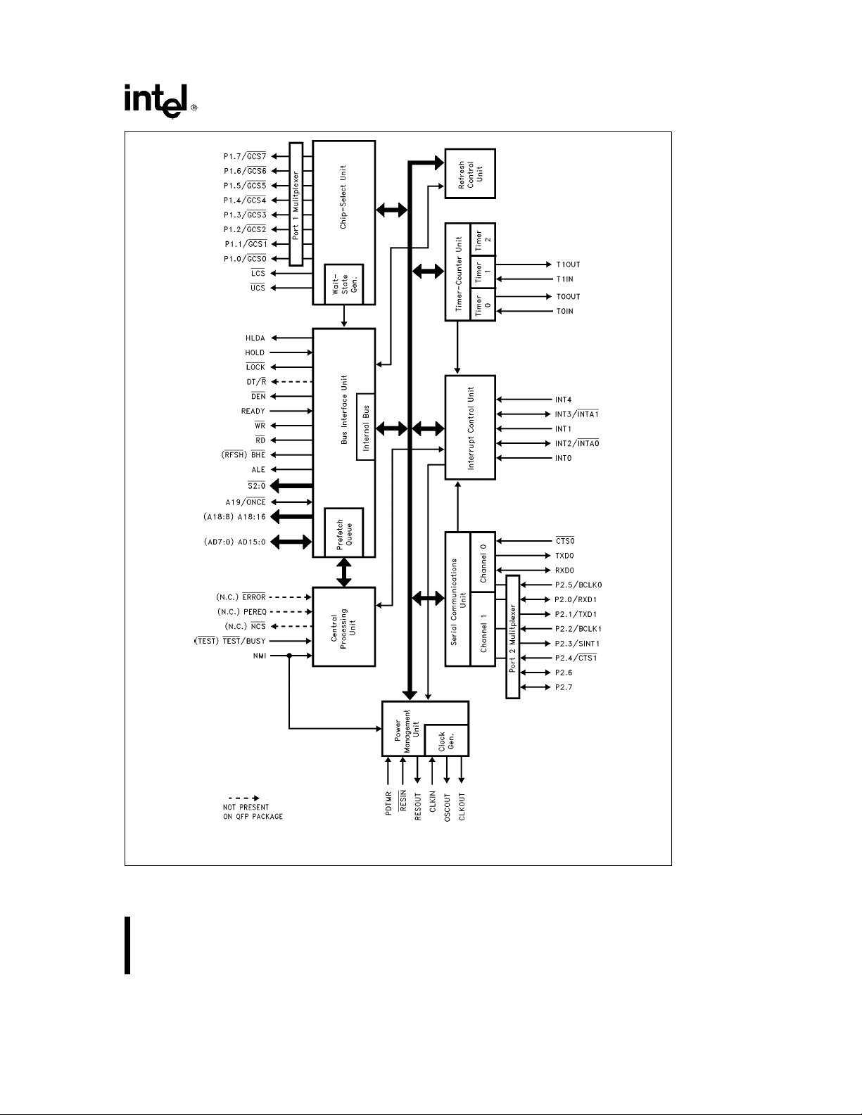
80C186EB/80C188EB, 80L186EB/80L188EB
NOTE:
Pin names in parentheses apply to the 80C188EB/80L188EB
Figure 1. 80C186EB/80C188EB Block Diagram
272433– 2
3
Page 4

80C186EB/80C188EB, 80L186EB/80L188EB
INTRODUCTION
Unless specifically noted, all references to the
80C186EB apply to the 80C188EB, 80L186EB, and
80L188EB. References to pins that differ between
the 80C186EB/80L186EB and the 80C188EB/
80L188EB are given in parentheses. The ‘‘L’’ in the
part number denotes low voltage operation. Physically and functionally, the ‘‘C’’ and ‘‘L’’ devices are
identical.
The 80C186EB is the first product in a new generation of low-power, high-integration microprocessors.
It enhances the existing 186 family by offering new
features and new operating modes. The 80C186EB
is object code compatible with the 80C186XL/
80C188XL microprocessors.
The 80L186EB is the 3V version of the 80C186EB.
The 80L186EB is functionally identical to the
80C186EB embedded processor. Current
80C186EB users can easily upgrade their designs to
use the 80L186EB and benefit from the reduced
power consumption inherent in 3V operation.
The feature set of the 80C186EB meets the needs
of low power, space critical applications. Low-Power
applications benefit from the static design of the
CPU core and the integrated peripherals as well as
low voltage operation. Minimum current consumption is achieved by providing a Powerdown mode
that halts operation of the device, and freezes the
clock circuits. Peripheral design enhancements ensure that non-initialized peripherals consume little
current.
Space critical applications benefit from the integration of commonly used system peripherals. Two
serial channels are provided for services such as
diagnostics, inter-processor communication, modem
interface, terminal display interface, and many others. A flexible chip select unit simplifies memory and
peripheral interfacing. The interrupt unit provides
sources for up to 129 external interrupts and will prioritize these interrupts with those generated from
the on-chip peripherals. Three general purpose timer/counters and sixteen multiplexed I/O port pins
round out the feature set of the 80C186EB.
Figure 1 shows a block diagram of the 80C186EB/
80C188EB. The Execution Unit (EU) is an enhanced
8086 CPU core that includes: dedicated hardware to
speed up effective address calculations, enhance
execution speed for multiple-bit shift and rotate instructions and for multiply and divide instructions,
string move instructions that operate at full bus
bandwidth, ten new instruction, and fully static operation. The Bus Interface Unit (BIU) is the same as
that found on the original 186 family products, ex-
cept the queue status mode has been deleted and
buffer interface control has been changed to ease
system design timings. An independent internal bus
is used to allow communication between the BIU
and internal peripherals.
CORE ARCHITECTURE
Bus Interface Unit
The 80C186EB core incorporates a bus controller
that generates local bus control signals. In addition,
it employs a HOLD/HLDA protocol to share the local
bus with other bus masters.
The bus controller is responsible for generating 20
bits of address, read and write strobes, bus cycle
status information, and data (for write operations) information. It is also responsible for reading data off
the local bus during a read operation. A READY input pin is provided to extend a bus cycle beyond the
minimum four states (clocks).
The local bus controller also generates two control
signals (DEN
nal transceiver chips. (Both DEN
available on the PLCC devices, only DEN
able on the QFP and SQFP devices.) This capability
allows the addition of transceivers for simple buffering of the multiplexed address/data bus.
and DT/R) when interfacing to exter-
and DT/R are
is avail-
Clock Generator
The processor provides an on-chip clock generator
for both internal and external clock generation. The
clock generator features a crystal oscillator, a divideby-two counter, and two low-power operating
modes.
The oscillator circuit is designed to be used with either a parallel resonant fundamental or third-overtone mode crystal network. Alternatively, the oscillator circuit may be driven from an external clock
source. Figure 2 shows the various operating modes
of the oscillator circuit.
The crystal or clock frequency chosen must be twice
the required processor operating frequency due to
the internal divide-by-two counter. This counter is
used to drive all internal phase clocks and the external CLKOUT signal. CLKOUT is a 50% duty cycle
processor clock and can be used to drive other system components. All AC timings are referenced to
CLKOUT.
4
Page 5
80C186EB/80C188EB, 80L186EB/80L188EB
272433– 4
(A) Crystal Connection
NOTE:
The L
overtone crystal.
The following parameters are recommended when
choosing a crystal:
Temperature Range: Application Specific
ESR (Equivalent Series Resistance): 40X max
C0 (Shunt Capacitance of Crystal): 7.0 pF max
C
L
Drive Level: 1 mW max
network is only required when using a third-
1C1
(Load Capacitance): 20 pFg2pF
272433– 3
Figure 2. Clock Configurations
80C186EB PERIPHERAL
ARCHITECTURE
The 80C186EB has integrated several common system peripherals with a CPU core to create a compact, yet powerful system. The integrated peripherals are designed to be flexible and provide logical
interconnections between supporting units (e.g., the
interrupt control unit supports interrupt requests
from the timer/counters or serial channels).
The list of integrated peripherals includes:
7-Input Interrupt Control Unit
#
3-Channel Timer/Counter Unit
#
2-Channel Serial Communications Unit
#
10-Output Chip-Select Unit
#
I/O Port Unit
#
Refresh Control Unit
#
Power Management Unit
#
The registers associated with each integrated periheral are contained within a 128 x 16 register file
called the Peripheral Control Block (PCB). The PCB
can be located in either memory or I/O space on
any 256 Byte address boundary.
(B) Clock Connection
Figure 3 provides a list of the registers associated
with the PCB. The Register Bit Summary at the end
of this specification individually lists all of the registers and identifies each of their programming attributes.
Interrupt Control Unit
The 80C186EB can receive interrupts from a number of sources, both internal and external. The interrupt control unit serves to merge these requests on
a priority basis, for individual service by the CPU.
Each interrupt source can be independently masked
by the Interrupt Control Unit (ICU) or all interrupts
can be globally masked by the CPU.
Internal interrupt sources include the Timers and Serial channel 0. External interrupt sources come from
the five input pins INT4:0. The NMI interrupt pin is
not controlled by the ICU and is passed directly to
the CPU. Although the Timer and Serial channel
each have only one request input to the ICU, separate vector types are generated to service individual
interrupts within the Timer and Serial channel units.
Timer/Counter Unit
The 80C186EB Timer/Counter Unit (TCU) provides
three 16-bit programmable timers. Two of these are
highly flexible and are connected to external pins for
control or clocking. A third timer is not connected to
any external pins and can only be clocked internally.
However, it can be used to clock the other two timer
channels. The TCU can be used to count external
events, time external events, generate non-repetitive waveforms, generate timed interrupts. etc.
5
Page 6
80C186EB/80C188EB, 80L186EB/80L188EB
PCB
Offset
00H Reserved
02H End Of Interrupt
04H Poll
06H Poll Status
08H Interrupt Mask
0AH Priority Mask
0CH In-Service
0EH Interrupt Request
10H Interrupt Status
12H Timer Control
14H Serial Control
16H INT4 Control
18H INT0 Control
1AH INT1 Control
1CH INT2 Control
1EH INT3 Control
20H Reserved
22H Reserved
24H Reserved
26H Reserved
28H Reserved
2AH Reserved
2CH Reserved
2EH Reserved
30H Timer0 Count
32H Timer0 Compare A
34H Timer0 Compare B
36H Timer0 Control
38H Timer1 Count
3AH Timer1 Compare A
3CH Timer1 Compare B
3EH Timer1 Control
Function
PCB
Offset
40H Timer2 Count
42H Timer2 Compare
44H Reserved
46H Timer2 Control
48H Reserved
4AH Reserved
4CH Reserved
4EH Reserved
50H Port 1 Direction
52H Port 1 Pin
54H Port 1 Control
56H Port 1 Latch
58H Port 2 Direction
5AH Port 2 Pin
5CH Port 2 Control
5EH Port 2 Latch
60H Serial0 Baud
62H Serial0 Count
64H Serial0 Control
66H Serial0 Status
68H Serial0 RBUF
6AH Serial0 TBUF
6CH Reserved
6EH Reserved
70H Serial1 Baud
72H Serial1 Count
74H Serial1 Control
76H Serial1 Status
78H Serial1 RBUF
7AH Serial1 TBUF
7CH Reserved
7EH Reserved
Function
PCB
Offset
80H GCS0 Start
82H GCS0 Stop
84H GCS1 Start
86H GCS1 Stop
88H GCS2 Start
8AH GCS2 Stop
8CH GCS3 Start
8EH GCS3 Stop
90H GCS4 Start
92H GCS4 Stop
94H GCS5 Start
96H GCS5 Stop
98H GCS6 Start
9AH GCS6 Stop
9CH GCS7 Start
9EH GCS7 Stop
A0H LCS Start
A2H LCS Stop
A4H UCS Start
A6H UCS Stop
A8H Relocation
AAH Reserved
ACH Reserved
AEH Reserved
B0H Refresh Base
B2H Refresh Time
B4H Refresh Control
B6H Reserved
B8H Power Control
BAH Reserved
BCH Step ID
BEH Reserved
Function
Figure 3. Peripheral Control Block Registers
PCB
Offset
C0H Reserved
C2H Reserved
C4H Reserved
C6H Reserved
C8H Reserved
CAH Reserved
CCH Reserved
CEH Reserved
D0H Reserved
D2H Reserved
D4H Reserved
D6H Reserved
D8H Reserved
DAH Reserved
DCH Reserved
DEH Reserved
E0H Reserved
E2H Reserved
E4H Reserved
E6H Reserved
E8H Reserved
EAH Reserved
ECH Reserved
EEH Reserved
F0H Reserved
F2H Reserved
F4H Reserved
F6H Reserved
F8H Reserved
FAH Reserved
FCH Reserved
FEH Reserved
Function
6
Page 7

80C186EB/80C188EB, 80L186EB/80L188EB
Serial Communications Unit
The Serial Control Unit (SCU) of the 80C186EB contains two independent channels. Each channel is
identical in operation except that only channel 0 is
supported by the integrated interrupt controller
(channel 1 has an external interrupt pin). Each
channel has its own baud rate generator that is independent of the Timer/Counter Unit, and can be
internally or externally clocked at up to one half the
80C186EB operating frequency.
Independent baud rate generators are provided for
each of the serial channels. For the asynchronous
modes, the generator supplies an 8x baud clock to
both the receive and transmit register logic. A 1x
baud clock is provided in the synchronous mode.
Chip-Select Unit
The 80C186EB Chip-Select Unit (CSU) integrates
logic which provides up to ten programmable chipselects to access both memories and peripherals. In
addition, each chip-select can be programmed to
automatically insert additional clocks (wait-states)
into the current bus cycle and automatically terminate a bus cycle independent of the condition of the
READY input pin.
I/O Port Unit
The I/O Port Unit (IPU) on the 80C186EB supports
two 8-bit channels of input, output, or input/output
operation. Port 1 is multiplexed with the chip select
pins and is output only. Most of Port 2 is multiplexed
with the serial channel pins. Port 2 pins are limited to
either an output or input function depending on the
operation of the serial pin it is multiplexed with.
Refresh Control Unit
The Refresh Control Unit (RCU) automatically generates a periodic memory read bus cycle to keep
dynamic or pseudo-static memory refreshed. A 9-bit
counter controls the number of clocks between refresh requests.
A 12-bit address generator is maintained by the RCU
and is presented on the A12:1 address lines during
the refresh bus cycle. Address bits A19:13 are programmable to allow the refresh address block to be
located on any 8 Kbyte boundary.
Power Management Unit
The 80C186EB Power Management Unit (PMU) is
provided to control the power consumption of the
device. The PMU provides three power modes: Active, Idle, and Powerdown.
Active Mode indicates that all units on the
80C186EB are functional and the device consumes
maximum power (depending on the level of peripheral operation). Idle Mode freezes the clocks of the
Execution and Bus units at a logic zero state (all
peripherals continue to operate normally).
The Powerdown mode freezes all internal clocks at
a logic zero level and disables the crystal oscillator.
All internal registers hold their values provided V
is maintained. Current consumption is reduced to
just transistor junction leakage.
CC
80C187 Interface (80C186EB Only)
The 80C186EB (PLCC package only) supports the
direct connection of the 80C187 Numerics Coprocessor.
ONCE Test Mode
To facilitate testing and inspection of devices when
fixed into a target system, the 80C186EB has a test
mode available which forces all output and input/
output pins to be placed in the high-impedance
state. ONCE stands for ‘‘ON Circuit Emulation’’. The
ONCE mode is selected by forcing the A19/ONCE
pin LOW (0) during a processor reset (this pin is
weakly held to a HIGH (1) level) while RESIN
tive.
is ac-
7
Page 8
80C186EB/80C188EB, 80L186EB/80L188EB
PACKAGE INFORMATION
This section describes the pins, pinouts, and thermal
characteristics for the 80C186EB in the Plastic
Leaded Chip Carrier (PLCC) package, Shrink Quad
Flat Pack (SQFP), and Quad Flat Pack (QFP) package. For complete package specifications and information, see the Intel Packaging Outlines and Dimensions Guide (Order Number: 231369).
Prefix Identification
With the extended temperature range, operational
characteristics are guaranteed over the temperature
range corresponding to
Package types are identified by a two-letter prefix to
the part number. The prefixes are listed in Table 1.
Table 1. Prefix Identification
Prefix Note
TN PLCC Extended
TS QFP (EIAJ) Extended
SB 1 SQFP Extended/Commercial
N 1 PLCC Commercial
S 1 QFP (EIAJ) Commercial
NOTE:
1. The 5V 25 MHz and 3V 16 MHz versions are only available in commercial temperature range corresponding to
Ctoa70§C ambient.
0
§
b
40§Ctoa85§C ambient.
Package Temperature
Type Type
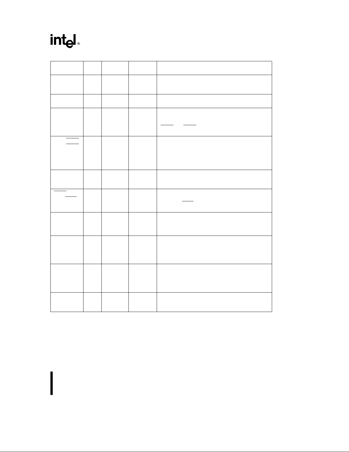
Pin Descriptions
Each pin or logical set of pins is described in Table
3. There are three columns for each entry in the Pin
Description Table.
The Pin Type column contains two kinds of information. The first symbol indicates whether a pin is power (P), ground (G), input only (I), output only (O) or
input/output (I/O). Some pins have multiplexed
functions (for example, A19/S6). Additional symbols
indicate additional characteristics for each pin. Table
2 lists all the possible symbols for this column.
The Input Type column indicates the type of input
(Asynchronous or Synchronous).
Asynchronous pins require that setup and hold times
be met only in order to guarantee
particular clock edge. Synchronous pins require that
setup and hold times be met to guarantee proper
operation.
time for the SRDY pin (a synchronous input) will result in a system failure or lockup. Input pins may also
be edge- or level-sensitive. The possible characteristics for input pins are S(E), S(L), A(E) and A(L).
The Output States column indicates the output
state as a function of the device operating mode.
Output states are dependent upon the current activity of the processor. There are four operational
states that are different from regular operation: bus
hold, reset, Idle Mode and Powerdown Mode. Appropriate characteristics for these states are also indicated in this column, with the legend for all possible characteristics in Table 2.
The Pin Description column contains a text description of each pin.
As an example, consider AD15:0. I/O signifies the
pins are bidirectional. S(L) signifies that the input
function is synchronous and level-sensitive. H(Z)
signifies that, as outputs, the pins are high-impedance upon acknowledgement of bus hold. R(Z) signifies that the pins float during reset. P(X) signifies
that the pins retain their states during Powerdown
Mode.
For example, missing the setup or hold
recognition
at a
The Pin Name column contains a mnemonic that
describes the pin function. Negation of the signal
name (for example, RESIN
active low.
8
) denotes a signal that is
Page 9

80C186EB/80C188EB, 80L186EB/80L188EB
Table 2. Pin Description Nomenclature
Symbol Description
P Power Pin (ApplyaVCCVoltage)
G Ground (Connect to V
I Input Only Pin
O Output Only Pin
I/O Input/Output Pin
S(E) Synchronous, Edge Sensitive
S(L) Synchronous, Level Sensitive
A(E) Asynchronous, Edge Sensitive
A(L) Asynchronous, Level Sensitive
H(1) Output Driven to VCCduring Bus Hold
H(0) Output Driven to V
H(Z) Output Floats during Bus Hold
H(Q) Output Remains Active during Bus Hold
H(X) Output Retains Current State during Bus Hold
R(WH) Output Weakly Held at VCCduring Reset
R(1) Output Driven to V
R(0) Output Driven to V
R(Z) Output Floats during Reset
R(Q) Output Remains Active during Reset
R(X) Output Retains Current State during Reset
I(1) Output Driven to VCCduring Idle Mode
I(0) Output Driven to V
I(Z) Output Floats during Idle Mode
I(Q) Output Remains Active during Idle Mode
I(X) Output Retains Current State during Idle Mode
P(1) Output Driven to VCCduring Powerdown Mode
P(0) Output Driven to V
P(Z) Output Floats during Powerdown Mode
P(Q) Output Remains Active during Powerdown Mode
P(X) Output Retains Current State during Powerdown Mode
)
SS
during Bus Hold
SS
during Reset
CC
during Reset
SS
during Idle Mode
SS
during Powerdown Mode
SS
9
Page 10
80C186EB/80C188EB, 80L186EB/80L188EB
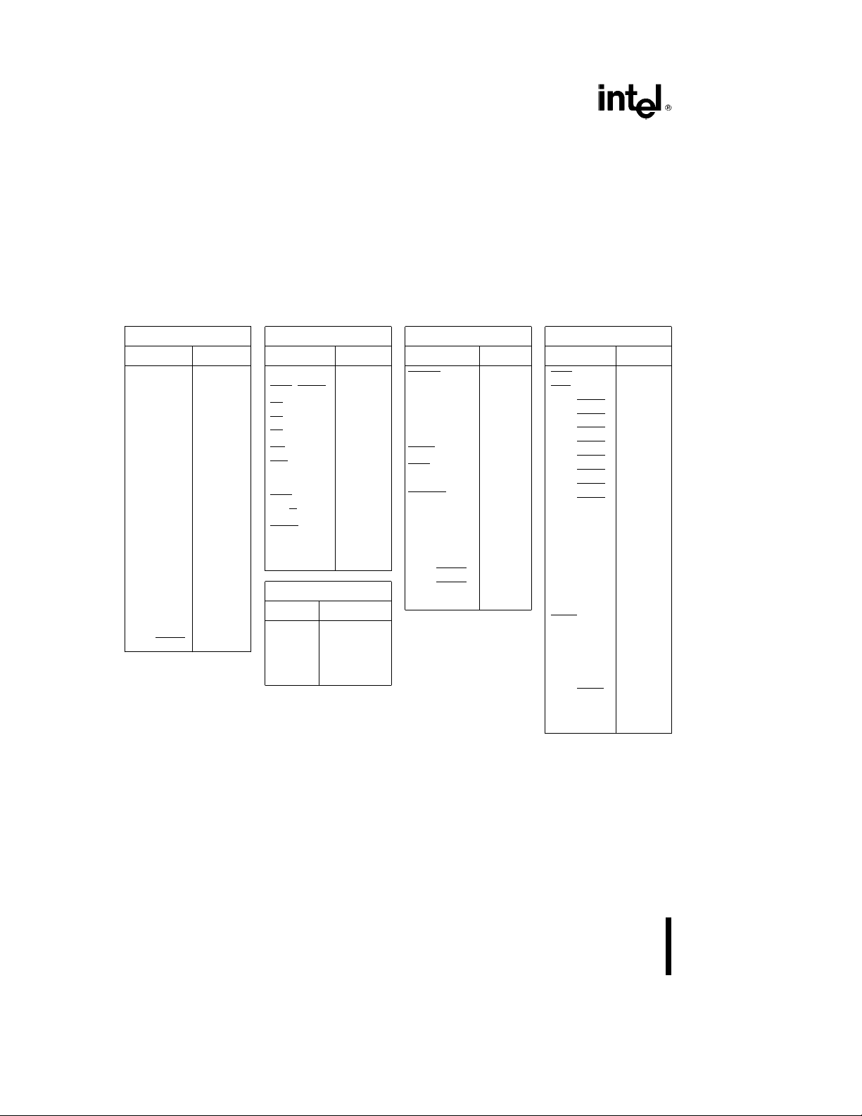
Table 3. Pin Descriptions
Pin Pin Input Output
Name Type Type States
V
CC
V
SS
PÐ ÐPOWER connections consist of four pins which must be
shorted externally to a V
GÐ ÐGROUND connections consist of six pins which must be
shorted externally to a V
CLKIN I A(E) Ð CLocK INput is an input for an external clock. An external
oscillator operating at two times the required processor
operating frequency can be connected to CLKIN. For crystal
operation, CLKIN (along with OSCOUT) are the crystal
connections to an internal Pierce oscillator.
OSCOUT O Ð H(Q) OSCillator OUTput is only used when using a crystal to
R(Q)
P(Q)
generate the external clock. OSCOUT (along with CLKIN)
are the crystal connections to an internal Pierce oscillator.
This pin is not to be used as 2X clock output for non-crystal
applications (i.e., this pin is N.C. for non-crystal applications).
OSCOUT does not float in ONCE mode.
CLKOUT O Ð H(Q) CLocK OUTput provides a timing reference for inputs and
R(Q)
P(Q)
outputs of the processor, and is one-half the input clock
(CLKIN) frequency. CLKOUT has a 50% duty cycle and
transistions every falling edge of CLKIN.
RESIN I A(L) Ð RESet IN causes the processor to immediately terminate
any bus cycle in progress and assume an initialized state. All
pins will be driven to a known state, and RESOUT will also
be driven active. The rising edge (low-to-high) transition
synchronizes CLKOUT with CLKIN before the processor
begins fetching opcodes at memory location 0FFFF0H.
RESOUT O Ð H(0) RESet OUTput that indicates the processor is currently in
R(1)
P(0)
the reset state. RESOUT will remain active as long as RESIN
remains active.
PDTMR I/O A(L) H(WH) Power-Down TiMeR pin (normally connected to an external
R(Z)
P(1)
capacitor) that determines the amount of time the processor
waits after an exit from power down before resuming normal
operation. The duration of time required will depend on the
startup characteristics of the crystal oscillator.
NMI I A(E) Ð Non-Maskable Interrupt input causes a TYPE-2 interrupt to
be serviced by the CPU. NMI is latched internally.
TEST/BUSY I A(E) Ð TEST is used during the execution of the WAIT instruction to
(TEST
)
suspend CPU operation until the pin is sampled active
(LOW). TEST is alternately known as BUSY when interfacing
with an 80C187 numerics coprocessor (80C186EB only).
AD15:0 I/O S(L) H(Z) These pins provide a multiplexed Address and Data bus.
(AD7:0) R(Z)
P(X)
During the address phase of the bus cycle, address bits 0
through 15 (0 through 7 on the 80C188EB) are presented on
the bus and can be latched using ALE. 8- or 16-bit data
information is transferred during the data phase of the bus
cycle.
Description
board plane.
CC
board plane.
SS
NOTE:
Pin names in parentheses apply to the 80C188EB/80L188EB.
10
Page 11
80C186EB/80C188EB, 80L186EB/80L188EB
Table 3. Pin Descriptions (Continued)
Pin Pin Input Output
Name Type Type States
A18:16 I/O A(L) H(Z) These pins provide multiplexed Address during the address
A19/ONCE
R(WH)
(A15:A8) P(X)
(A18:16)
(A19/ONCE)
phase of the bus cycle. Address bits 16 through 19 are presented
on these pins and can be latched using ALE. These pins are
driven to a logic 0 during the data phase of the bus cycle. On the
80C188EB, A15–A8 provide valid address information for the
entire bus cycle. During a processor reset (RESIN
ONCE
is used to enable ONCE mode. A18:16 must not be driven
low during reset or improper operation may result.
S2:0 O Ð H(Z) Bus cycle Status are encoded on these pins to provide bus
transaction information. S2:0
R(Z)
P(1)
S1 S0 Bus Cycle Initiated
S2
0 0 0 Interrupt Acknowledge
0 0 1 Read I/O
0 1 0 Write I/O
0 1 1 Processor HALT
1 0 0 Queue Instruction Fetch
1 0 1 Read Memory
1 1 0 Write Memory
1 1 1 Passive (no bus activity)
ALE O Ð H(0) Address Latch Enable output is used to strobe address
information into a transparent type latch during the address phase
R(0)
of the bus cycle.
P(0)
BHE O Ð H(Z) Byte High Enable output to indicate that the bus cycle in progress
) R(Z)
(RFSH
is transferring data over the upper half of the data bus. BHE
A0 have the following logical encoding
P(X)
A0 BHE Encoding (for the 80C186EB/80L186EB only)
0 0 Word Transfer
0 1 Even Byte Transfer
1 0 Odd Byte Transfer
1 1 Refresh Operation
On the 80C188EB/80L188EB, RFSH is asserted low to indicate a
refresh bus cycle.
RD O Ð H(Z) ReaD output signals that the accessed memory or I/O device
must drive data information onto the data bus.
R(Z)
P(1)
WR O Ð H(Z) WRite output signals that data available on the data bus are to be
written into the accessed memory or I/O device.
R(Z)
P(1)
READY I A(L) Ð READY input to signal the completion of a bus cycle. READY
S(L)
must be active to terminate any bus cycle, unless it is ignored by
correctly programming the Chip-Select Unit.
DEN O Ð H(Z) Data ENable output to control the enable of bi-directional
transceivers in a buffered system. DEN
R(Z)
to be transferred on the bus.
P(1)
Description
active), A19/
are encoded as follows:
and
is active only when data is
NOTE:
Pin names in parentheses apply to the 80C188EB/80L188EB.
11
Page 12
80C186EB/80C188EB, 80L186EB/80L188EB
Table 3. Pin Descriptions (Continued)
Pin Pin Input Output
Name Type Type States
DT/R O Ð H(Z) Data Transmit/Receive output controls the direction of a
R(Z)
P(X)
bi-directional buffer in a buffered system. DT/R
available for the PLCC package.
LOCK O Ð H(Z) LOCK output indicates that the bus cycle in progress is not
R(WH)
P(1)
to be interrupted. The processor will not service other bus
requests (such as HOLD) while LOCK
configured as a weakly held high input while RESIN
active and must not be driven low.
HOLD I A(L) Ð HOLD request input to signal that an external bus master
wishes to gain control of the local bus. The processor will
relinquish control of the local bus between instruction
boundaries not conditioned by a LOCK prefix.
HLDA O Ð H(1) HoLD Acknowledge output to indicate that the processor
R(0)
P(0)
has relinquished control of the local bus. When HLDA is
asserted, the processor will (or has) floated its data bus
and control signals allowing another bus master to drive the
signals directly.
NCS O Ð H(1) Numerics Coprocessor Select output is generated when
(N.C.) R(1)
P(1)
accessing a numerics coprocessor. NCS is not provided on
the QFP or SQFP packages. This signal does not exist on
the 80C188EB/80L188EB.
ERROR I A(L) Ð ERROR input that indicates the last numerics coprocessor
(N.C.)
operation resulted in an exception condition. An interrupt
TYPE 16 is generated if ERROR
beginning of a numerics operation. ERROR
on the QFP or SQFP packages. This signal does not exist
on the 80C188EB/80L188EB.
PEREQ I A(L) Ð CoProcessor REQuest signals that a data transfer
(N.C.)
between an External Numerics Coprocessor and Memory is
pending. PEREQ is not provided on the QFP or SQFP
packages. This signal does not exist on the 80C188EB/
80L188EB.
UCS O Ð H(1) Upper Chip Select will go active whenever the address of
R(1)
P(1)
a memory or I/O bus cycle is within the address limitations
programmed by the user. After reset, UCS
be active for memory accesses between 0FFC00H and
0FFFFFH.
LCS O Ð H(1) Lower Chip Select will go active whenever the address of
R(1)
P(1)
a memory bus cycle is within the address limitations
programmed by the user. LCS
P1.0/GCS0 O Ð H(X)/H(1) These pins provide a multiplexed function. If enabled, each
P1.1/GCS1
P1.2/GCS2
P1.3/GCS3
P1.4/GCS4
P1.5/GCS5
P1.6/GCS6
R(1)
P(X)/P(1)
pin can provide a Generic Chip Select output which will go
active whenever the address of a memory or I/O bus cycle
is within the address limitations programmed by the user.
When not programmed as a Chip-Select, each pin may be
used as a general purpose output Port. As an output port
pin, the value of the pin can be read internally.
P1.7/GCS7
Description
is only
is active. This pin is
is
is sampled active at the
is not provided
is configured to
is inactive after a reset.
NOTE:
Pin names in parentheses apply to the 80C188EB/80L188EB.
12
Page 13
80C186EB/80C188EB, 80L186EB/80L188EB
Table 3. Pin Descriptions (Continued)
Pin Pin Input Output
Name Type Type States
T0OUT O Ð H(Q) Timer OUTput pins can be programmed to provide a
T1OUT R(1)
P(Q)
single clock or continuous waveform generation,
depending on the timer mode selected.
T0IN I A(L) Ð Timer INput is used either as clock or control signals,
T1IN A(E)
depending on the timer mode selected.
INT0 I A(E,L) Ð Maskable INTerrupt input will cause a vector to a
INT1
INT4
specific Type interrupt routine. To allow interrupt
expansion, INT0 and/or INT1 can be used with
INTA0
and INTA1 to interface with an external slave
controller.
INT2/INTA0 I/O A(E,L) H(1) These pins provide a multiplexed function. As inputs,
INT3/INTA1
R(Z)
P(1)
they provide a maskable INTerrupt that will cause
the CPU to vector to a specific Type interrupt routine.
As outputs, each is programmatically controlled to
provide an INTERRUPT ACKNOWLEDGE
handshake signal to allow interrupt expansion.
P2.7 I/O A(L) H(X) BI-DIRECTIONAL, open-drain Port pins.
P2.6 R(Z)
P(X)
CTSO I A(L) Ð Clear-To-Send input is used to prevent the
P2.4/CTS1
transmission of serial data on their respective TXD
signal pin. CTS1 is multiplexed with an input only port
function.
TXD0 O Ð H(X)/H(Q) Transmit Data output provides serial data
P2.1/TXD1 R(1)
P(X)/P(Q)
information. TXD1 is multiplexed with an output only
Port function. During synchronous serial
communications, TXD will function as a clock output.
RXD0 I/O A(L) R(Z) Receive Data input accepts serial data information.
P2.0/RXD1 H(Q)
P(X)
RXD1 is multiplexed with an input only Port function.
During synchronous serial communications, RXD is
bi-directional and will become an output for
transmission or data (TXD becomes the clock).
P2.5/BCLK0 I A(L)/A(E) Ð Baud CLocK input can be used as an alternate clock
P2.2/BCLK1
source for each of the integrated serial channels.
BCLKx is multiplexed with an input only Port function,
and cannot exceed a clock rate greater than one-half
the operating frequency of the processor.
P2.3/SINT1 O Ð H(X)/H(Q) Serial INTerrupt output will go active to indicate
R(0)
P(X)/P(X)
serial channel 1 requires service. SINT1 is
multiplexed with an output only Port function.
Description
NOTE:
Pin names in parentheses apply to the 80C188EB/80L188EB.
13
Page 14
80C186EB/80C188EB, 80L186EB/80L188EB
80C186EB PINOUT
Tables 4 and 5 list the 80C186EB/80C188EB pin
names with package location for the 84-pin Plastic
Leaded Chip Carrier (PLCC) component. Figure 5
depicts the complete 80C186EB/80C188EB pinout
(PLCC package) as viewed from the top side of the
component (i.e., contacts facing down).
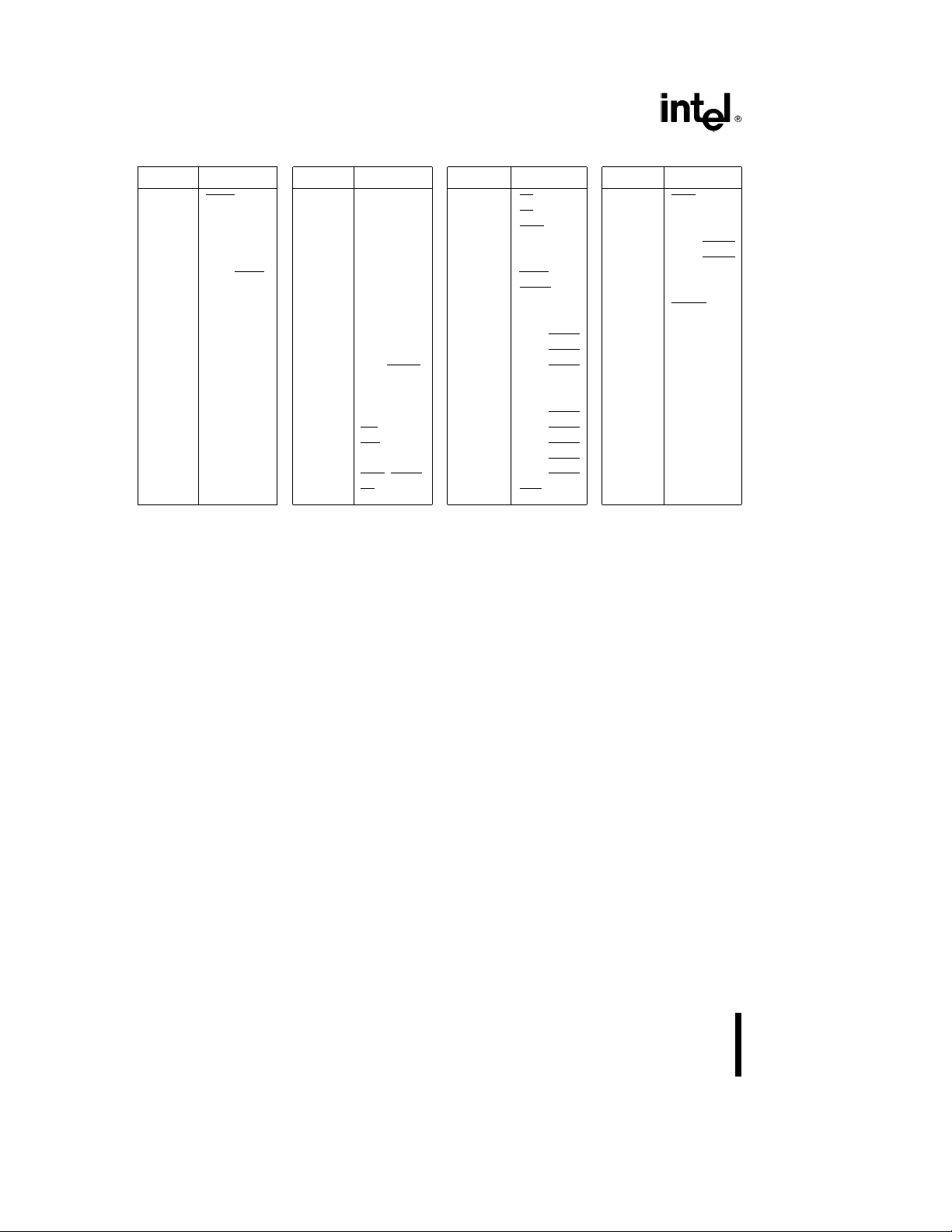
Table 4. PLCC Pin Names with Package Location
Address/Data Bus
Name Location
AD0 61
AD1 66
AD2 68
AD3 70
AD4 72
AD5 74
AD6 76
AD7 78
AD8 (A8) 62
AD9 (A9) 67
AD10 (A10) 69
AD11 (A11) 71
AD12 (A12) 73
AD13 (A13) 75
AD14 (A14) 77
AD15 (A15) 79
A16 80
A17 81
A18 82
A19/ONCE
NOTE:
Pin names in parentheses apply to the 80C188EB/80L188EB.
83
Bus Control
Name Location
ALE 6
BHE
(RFSH)7
S0
S1
S2 8
RD 4
WR
READY 18
DEN
DT/R
LOCK 15
HOLD 13
HLDA 12
Power
Name Location
V
SS
V
CC
10
11
16
2, 22, 43
63, 65, 84
1, 23
42, 64
9
5
Tables 6 and 7 list the 80C186EB/80C188EB pin
names with package location for the 80-pin Quad
Flat Pack (QFP) component. Figure 6 depicts the
complete 80C186EB/80C188EB (QFP package) as
viewed from the top side of the component (i.e., contacts facing down).
Tables 8 and 9 list the 80186EB/80188EB pin
names with package location for the 80-pin Shrink
Quad Flat Pack (SQFP) component. Figure 7 depicts
the complete 80C186EB/80C188EB (SQFP package) as viewed from the top side of the component
(i.e., contacts facing down).
Processor Control
Name Location
RESIN 37
RESOUT 38
CLKIN 41
OSCOUT 40
CLKOUT 44
TEST/BUSY 14
(N.C.) 60
NCS
PEREQ (N.C.) 39
ERROR
(N.C.) 3
PDTMR 36
NMI 17
INT0 31
INT1 32
INT2/INTA0
INT3/INTA1
INT4 35
33
34
UCS 30
LCS
P1.0/GCS0
P1.1/GCS1
P1.2/GCS2 26
P1.3/GCS3 25
P1.4/GCS4
P1.5/GCS5
P1.6/GCS6
P1.7/GCS7
T0OUT 45
T0IN 46
T1OUT 47
T1IN 48
RXD0 53
TXD0 52
P2.5/BCLK0 54
CTS0
P2.0/RXD1 57
P2.1/TXD1 58
P2.2/BCLK1 59
P2.3/SINT1 55
P2.4/CTS1
P2.6 50
P2.7 49
I/O
Name Location
29
28
27
24
21
20
19
51
56
14
Page 15
Table 5. PLCC Package Locations with Pin Name
Location Name
1V
CC
2V
SS
3 ERROR (N.C.)
4RD
5WR
6 ALE
7 BHE
(RFSH)
8S2
9S1
10 S0
11 DEN
12 HLDA
13 HOLD
14 TEST
/BUSY
15 LOCK
16 DT/R
17 NMI
18 READY
19 P1.7/GCS7
20 P1.6/GCS6
21 P1.5/GCS5
NOTE:
Pin names in parentheses apply to the 80C188EB/80L188EB.
Location Name
22 V
23 V
SS
CC
24 P1.4/GCS4
25 P1.3/GCS3
26 P1.2/GCS2
27 P1.1/GCS1
28 P1.0/GCS0
29 LCS
30 UCS
31 INT0
32 INT1
33 INT2/INTA0
34 INT3/INTA1
35 INT4
36 PDTMR
37 RESIN
38 RESOUT
39 PEREQ (N.C.)
40 OSCOUT
41 CLKIN
42 V
CC
80C186EB/80C188EB, 80L186EB/80L188EB
Location Name
43 V
SS
44 CLKOUT
45 T0OUT
46 T0IN
47 T1OUT
48 T1IN
49 P2.7
50 P2.6
51 CTS0
52 TXD0
53 RXD0
54 P2.5/BCLK0
55 P2.3/SINT1
56 P2.4/CTS1
57 P2.0/RXD1
58 P2.1/TXD1
59 P2.2/BCLK1
60 NCS
(N.C.)
61 AD0
62 AD8 (A8)
63 V
SS
Location Name
64 V
65 V
CC
SS
66 AD1
67 AD9 (A9)
68 AD2
69 AD10 (A10)
70 AD3
71 AD11 (A11)
72 AD4
73 AD12 (A12)
74 AD5
75 AD13 (A13)
76 AD6
77 AD14 (A14)
78 AD7
79 AD15 (A15)
80 A16
81 A17
82 A18
83 A19/ONCE
84 V
SS
15
Page 16
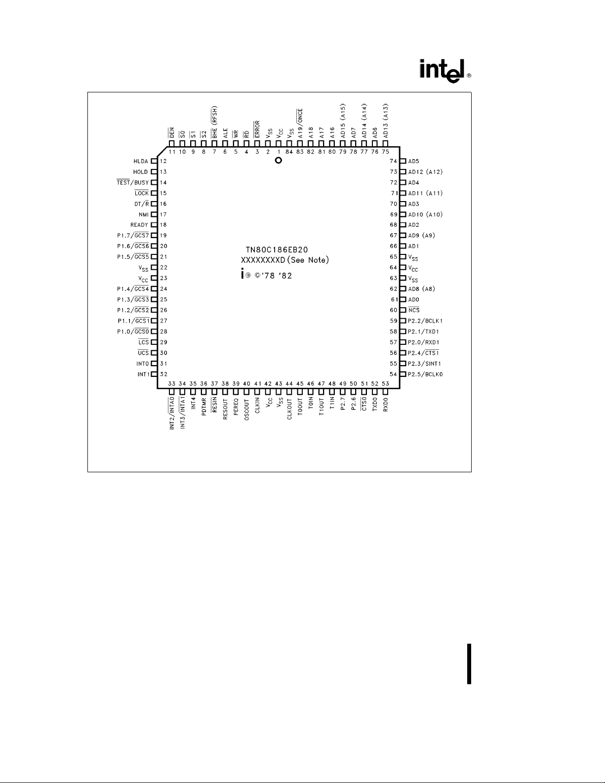
80C186EB/80C188EB, 80L186EB/80L188EB
NOTE:
This is the FPO number location (indicated by X’s).
Pin names in parentheses apply to the 80C188EB/80L188EB.
Figure 4. 84-Pin Plastic Leaded Chip Carrier Pinout Diagram
16
272433– 5
Page 17
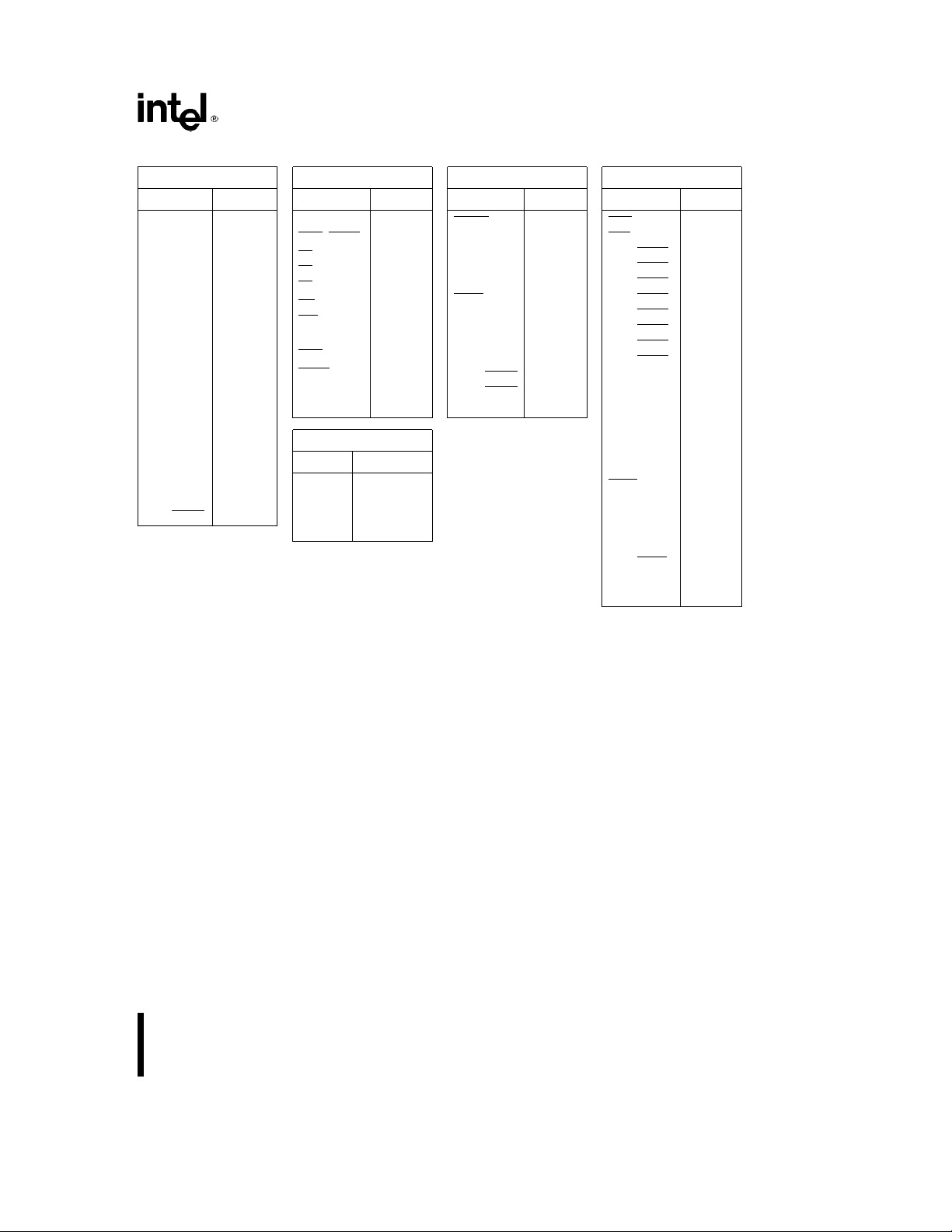
Table 6. QFP Pin Name with Package Location
Address/Data Bus
Name Location
AD0 10
AD1 15
AD2 17
AD3 19
AD4 21
AD5 23
AD6 25
AD7 27
AD8 (A8) 11
AD9 (A9) 16
AD10 (A10) 18
AD11 (A11) 20
AD12 (A12) 22
Bus Control
Name Location
ALE 38
BHE
(RFSH)39
S0
S1
42
41
S2 40
RD 36
WR
37
READY 49
DEN
LOCK
43
47
HOLD 45
HLDA 44
AD13 (A13) 24
AD14 (A14) 26
AD15 (A15) 28
A16 29
A17 30
A18 31
A19/ONCE
32
Power
Name Location
V
SS
12, 14, 33
35, 53, 73
V
CC
13, 34
54, 72
NOTE:
Pin names in parentheses apply to the 80C188EB/80L188EB.
80C186EB/80C188EB, 80L186EB/80L188EB
Processor Control
Name Location
RESIN 68
RESOUT 69
CLKIN 71
OSCOUT 70
CLKOUT 74
TEST 46
PDTMR 67
NMI 48
INT0 62
INT1 63
INT2/INTA0
64
INT3/INTA1 65
INT4 66
UCS 61
LCS
P1.0/GCS0
P1.1/GCS1
P1.2/GCS2 57
P1.3/GCS3 56
P1.4/GCS4
P1.5/GCS5
P1.6/GCS6
P1.7/GCS7
T0OUT 75
T0IN 76
T1OUT 77
T1IN 78
RXD0 3
TXD0 2
P2.5/BCLK0 4
CTS0
P2.0/RXD1 7
P2.1/TXD1 8
P2.2/BCLK1 9
P2.3/SINT1 5
P2.4/CTS1
P2.6 80
P2.7 79
I/O
Name Location
60
59
58
55
52
51
50
1
6
17
Page 18
80C186EB/80C188EB, 80L186EB/80L188EB
Table 7. QFP Package Location with Pin Names
Location Name
1 CTS0
2 TXD0
3 RXD0
4 P2.5/BCLK0
5 P2.3/SINT1
6 P2.4/CTS1
7 P2.0/RXD1
8 P2.1/TXD1
9 P2.2/BCLK1
10 AD0
11 AD8 (A8)
12 V
13 V
14 V
SS
CC
SS
15 AD1
16 AD9 (A9)
17 AD2
18 AD10 (A10)
19 AD3
20 AD11 (A11)
NOTE:
Pin names in parentheses apply to the 80C188EB/80L188EB.
Location Name
21 AD4
22 AD12 (A12)
23 AD5
24 AD13 (A13)
25 AD6
26 AD14 (A14)
27 AD7
28 AD15 (A15)
29 A16
30 A17
31 A18
32 A19/ONCE
33 V
34 V
35 V
SS
CC
SS
36 RD
37 WR
38 ALE
39 BHE
(RFSH)
40 S2
Location Name
41 S1
42 S0
43 DEN
44 HLDA
45 HOLD
46 TEST
47 LOCK
48 NMI
49 READY
50 P1.7/GCS7
51 P1.6/GCS6
52 P1.5/GCS5
53 V
54 V
SS
CC
55 P1.4/GCS4
56 P1.3/GCS3
57 P1.2/GCS2
58 P1.1/GCS1
59 P1.0/GCS0
60 LCS
Location Name
61 UCS
62 INT0
63 INT1
64 INT2/INTA0
65 INT3/INTA1
66 INT4
67 PDTMR
68 RESIN
69 RESOUT
70 OSCOUT
71 CLKIN
72 V
73 V
CC
SS
74 CLKOUT
75 T0OUT
76 T0IN
77 T1OUT
78 T1IN
79 P2.7
80 P2.6
18
Page 19

80C186EB/80C188EB, 80L186EB/80L188EB
NOTE:
This is the FPO number location (indicated by X’s).
Pin names in parentheses apply to the 80C188EB/80L188EB.
Figure 5. Quad Flat Pack Pinout Diagram
272433– 6
19
Page 20

80C186EB/80C188EB, 80L186EB/80L188EB
Table 8. SQFP Pin Functions with Location
AD Bus
AD0 47
AD1 52
AD2 54
AD3 56
AD4 58
AD5 60
AD6 62
AD7 64
AD8 (A8) 48
AD9 (A9) 53
AD10 (A10) 55
AD11 (A11) 57
AD12 (A12) 59
AD13 (A13) 61
AD14 (A14) 63
AD15 (A15) 65
A16 66
A17 67
A18 68
A19/ONCE 69
1 HLDA
2 HOLD
3 TEST
4 LOCK
Ý
Ý
5 NMI
6 READY
7 P1.7/GCS7
8 P1.6/GCS6
9 P1.5/GCS5
10 V
SS
11 V
CC
12 P1.4/GCS4
13 P1.3/GCS3
14 P1.2/GCS2
15 P1.1/GCS1
16 P1.0/GCS0
17 LCS
18 UCS
Ý
Ý
Ý
Ý
Ý
Ý
Ý
Ý
Ý
Ý
19 INT0
20 INT1
Bus Control
ALE 75
Ý
BHE
(RFSHÝ)76
S0
S1
S2
RD
WR
Ý
Ý
Ý
Ý
Ý
79
78
77
73
74
READY 6
Ý
DEN
LOCK
Ý
80
HOLD 2
HLDA 1
Table 9. SQFP Pin Locations with Pin Names
21 INT1/INTA0
22 INT3/INTA1
Ý
Ý
23 INT4
24 PDTMR
25 RESIN
Ý
26 RESOUT
27 OSCOUT
28 CLKIN
29 V
CC
30 V
SS
31 CLKOUT
32 T0OUT
33 T0IN
34 T1OUT
35 T1IN
36 P2.7
37 P2.6
38 CTS0
Ý
39 TXD0
40 RXD0
Processor Control
Ý
RESIN
RESOUT 26
CLKIN 28
OSCOUT 27
CLKOUT 31
TESTÝ/BUSY 3
NMI 5
INT0 19
INT1 20
INT2/INTA0
4
INT3/INTA1
INT4 23
PDTMR 24
Power and Ground
V
CC
V
CC
V
CC
V
CC
V
SS
V
SS
V
SS
V
SS
V
SS
V
SS
41 P2.5/BCLK0
42 P2.3/SINT1
43 P2.4/CTS1
44 P2.0/RXD1
45 P2.1/TXD1
46 P2.2/BCLK1
47 AD0
48 AD8 (A8)
49 V
SS
50 V
CC
51 V
SS
52 AD1
53 AD9 (A9)
54 AD2
55 AD10 (A10)
56 AD3
57 AD11 (A11)
58 AD4
59 AD12 (A12)
60 AD5
I/O
25
Ý
21
Ý
22
Ý
UCS
Ý
LCS
P1.0/GCS0
P1.1/GCS1
P1.2/GCS2
P1.3/GCS3
P1.4/GCS4
P1.5/GCS5
P1.6/GCS6
P1.7/GCS7
18
17
Ý
Ý
Ý
Ý
Ý
Ý
Ý
Ý
16
15
14
13
12
9
8
7
P2.0/RXD1 44
P2.1/TXD1 45
P2.2/BCLK1 46
P2.3/SINT1 42
11
P2.4/CTS1
29
P2.5/BCLK0 41
50
P2.6 37
71
P2.7 36
Ý
43
10
30
49
51
Ý
CTS0
38
TXD0 39
RXD0 40
70
72
T0IN 33
T1IN 35
T0OUT 32
T1OUT 34
61 AD13 (A13)
62 AD6
Ý
63 AD14 (A14)
64 AD7
65 AD15 (A15)
66 A16
67 A17
68 A18
69 A19/ONCE
70 V
SS
71 V
CC
72 V
SS
Ý
73 RD
74 WR
Ý
75 ALE
76 BHEÝ(RFSHÝ)
Ý
77 S2
Ý
78 S1
Ý
79 S0
80 DEN
Ý
NOTE:
Pin names in parentheses apply to the 80C188EB/80L188EB.
20
Page 21

80C186EB/80C188EB, 80L186EB/80L188EB
NOTE:
XXXXXXXXC indicates Intel FPO number.
Pin names in parentheses apply to the 80C188EB/80L188EB.
Figure 6. SQFP Package
272433– 7
21
Page 22

80C186EB/80C188EB, 80L186EB/80L188EB
PACKAGE THERMAL
SPECIFICATIONS
The 80C186EB/80L186EB is specified for operation
when T
of
a
any environment to determine whether the processor is within the specified operating range. The case
temperature must be measured at the center of the
top surface.
(the case temperature) is within the range
C
b
40§Ctoa100§C (PLCC package) orb40§Cto
114§C (QFP package). TCmay be measured in
(the ambient temperature) can be calculated
T
A
from i
ent) with the following equation:
(thermal resistance from the case to ambi-
CA
e
T
b
T
A
P*i
C
CA
Typical values for iCAat various airflows are given
in Table 10. P (the maximum power consumption,
specified in watts) is calculated by using the maximum ICC as tabulated in the DC specifications and
V
of 5.5V.
CC
Table 10. Thermal Resistance (i
) at Various Airflows (in§C/Watt)
CA
Airflow Linear ft/min (m/sec)
0 200 400 600 800 1000
(0) (1.01) (2.03) (3.04) (4.06) (5.07)
iCA(PLCC) 30 24 21 19 17 16.5
iCA(QFP) 58 47 43 40 38 36
iCA(SQFP) 70 TBD TBD TBD TBD TBD
22
Page 23

80C186EB/80C188EB, 80L186EB/80L188EB
ELECTRICAL SPECIFICATIONS
Absolute Maximum Ratings
Storage Temperature ААААААААААb65§Ctoa150§C
Case Temp under Bias АААААААААb65§Ctoa120§C
Supply Voltage
with Respect to V
Voltage on other Pins
with Respect to V
АААААААААААb0.5V toa6.5V
SS
ААААААb0.5V to V
SS
CC
a
0.5V
Recommended Connections
Power and ground connections must be made to
multiple V
circuit board should include separate power (V
and ground (V
connected to the power plane, and every V
must be connected to the ground plane. Pins identified as ‘‘NC’’ must not be connected in the system.
Liberal decoupling capacitance should be placed
near the processor. The processor can cause transient power surges when its output buffers transition, particularly when connected to large capacitive loads.
and VSSpins. Every 80C186EB-based
CC
) planes. Every VCCpin must be
SS
SS
CC
pin
NOTICE: This data sheet contains preliminary information on new products in production. It is valid for
the devices indicated in the revision history. The
specifications are subject to change without notice.
*
WARNING: Stressing the device beyond the ‘‘Absolute
Maximum Ratings’’ may cause permanent damage.
These are stress ratings only. Operation beyond the
‘‘Operating Conditions’’ is not recommended and extended exposure beyond the ‘‘Operating Conditions’’
may affect device reliability.
Low inductance capacitors and interconnects are
recommended for best high frequency electrical performance. Inductance is reduced by placing the decoupling capacitors as close as possible to the processor V
)
and VSSpackage pins.
CC
Always connect any unused input to an appropriate
signal level. In particular, unused interrupt inputs
(INT0:4) should be connected to V
up resistor (in the range of 50 KX). Leave any un-
through a pull-
CC
used output pin or any NC pin unconnected.
23
Page 24

80C186EB/80C188EB, 80L186EB/80L188EB
DC SPECIFICATIONS (80C186EB/80C188EB)
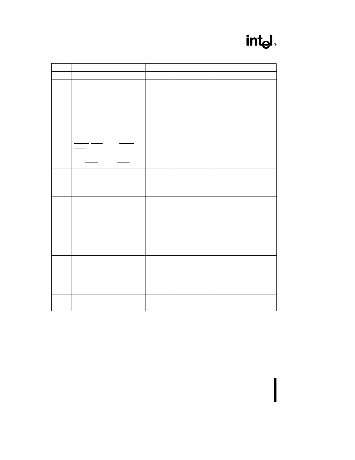
Symbol Parameter Min Max Units Notes
V
CC
V
IL
V
IH
V
OL
V
OH
V
HYR
I
LI1
I
LI2
I
LI3
I
LO
I
CC
I
ID
I
PD
C
IN
C
OUT
NOTES:
1. These pins have an internal pull-up device that is active while RESIN
current than specified (on any of these pins) may invoke a factory test mode.
2. Tested by outputs being floated by invoking ONCE Mode or by asserting HOLD.
3. Measured with the device in RESET and at worst case frequency, V
specified in AC Test Conditions, and all floating outputs driven to V
4. Measured with the device in HALT (IDLE Mode active) and at worst case frequency, V
outputs loaded as specified in AC Test Conditions, and all floating outputs driven to V
5. Measured with the device in HALT (Powerdown Mode active) and at worst case frequency, V
ALL outputs loaded as specified in AC Test Conditions, and all floating outputs driven to V
6. Output Capacitance is the capacitive load of a floating output pin.
7. Operating temperature for 25 MHz is 0
Supply Voltage 4.5 5.5 V
Input Low Voltage
Input High Voltage 0.7 V
Output Low Voltage 0.45 V I
Output High Voltage V
b
0.5 0.3 V
CCVCC
b
0.5 V I
CC
CC
a
0.5 V
V
e
OL
eb
OH
Input Hysterisis on RESIN 0.50 V
Input Leakage Current for Pins:
g
15 mA0VsV
AD15:0 (AD7:0), READY, HOLD,
RESIN
, CLKIN, TEST, NMI, INT4:0,
T0IN, T1IN, RXD0, BCLK0
, CTS0,
RXD1, BCLK1, CTS1, P2.6, P2.7
Input Leakage Current for Pins:
g
0.275
g
7mA0V
s
ERROR, PEREQ
Input Leakage Current for Pins:
A19/ONCE
, A18:16, LOCK
Output Leakage Current
b
0.275
b
5.0 mA V
g
15 mA 0.45sV
IN
e
(Note 2)
Supply Current Cold (RESET)
80C186EB25 115 mA (Notes 3, 7)
80C186EB20 108 mA (Note 3)
80C186EB13 73 mA (Note 3)
Supply Current Idle
80C186EB25 91 mA (Notes 4, 7)
80C186EB20 76 mA (Note 4)
80C186EB13 48 mA (Note 4)
Supply Current Powerdown
80C186EB25 100 mA (Notes 5, 7)
80C186EB20 100 mA (Note 5)
80C186EB13 100 mA (Note 5)
Input Pin Capacitance 0 15 pF T
Output Pin Capacitance 0 15 pF T
is low and ONCE Mode is not active. Sourcing more
, and temperature with ALL outputs loaded as
CC
or GND.
CC
or GND.
CC
Cto70§C, V
§
CC
e
5.0g10%.
e
F
e
F
, and temperature with ALL
CC
, and temperature with
CC
or GND.
CC
3 mA (Min)
2 mA (MIn)
s
IN
k
V
IN
0.7 VCC(Note 1)
OUT
1 MHz
1 MHz (Note 6)
V
CC
V
CC
s
V
CC
24
Page 25

80C186EB/80C188EB, 80L186EB/80L188EB
DC SPECIFICATIONS (80L186EB16) (operating temperature, 0
Cto70§C)
§
Symbol Parameter Min Max Units Notes
V
V
V
V
V
V
I
CC
IL
IH
OL
OH
HYR
LI1
Supply Voltage 3.0 5.5 V
Input Low Voltage
Input High Voltage 0.7 V
b
0.5 0.3 V
CCVCC
CC
a
0.5 V
V
Output Low Voltage 0.45 V I
Output High Voltage V
b
0.5 V I
CC
Input Hysterisis on RESIN 0.50 V
Input Leakage Current for pins:
g
15 mA0VsV
e
1.6 mA (Min) (Note 1)
OL
eb
1 mA (Min) (Note 1)
OH
s
V
IN
AD15:0 (AD7:0), READY, HOLD,
RESIN
, CLKIN, TEST, NMI,
INT4:0, T0IN, T1IN, RXD0,
BCLK0, CTS0, RXD1, BCLK1,
CTS1
, SINT1, P2.6, P2.7
I
I
I
LI2
LO
CC3
Input Leakage Current for Pins:
A19/ONCE
, A18:16, LOCK
Output Leakage Current
Supply Current (RESET, 3.3V)
b
0.275
b
2mAV
g
15 mA 0.45sV
IN
e
0.7 VCC(Note 2)
OUT
80L186EB16 54 mA (Note 4)
I
ID3
Supply Current Idle (3.3V)
80L186EB16 38 mA (Note 5)
I
PD3
Supply Current Powerdown (3.3V)
80L186EB16 40 mA (Note 6)
C
IN
C
OUT
NOTES:
1. I
2. These pins have an internal pull-up device that is active while RESIN
current than specified (on any of these pins) may invoke a factory test mode.
3. Tested by outputs being floated by invoking ONCE Mode or by asserting HOLD.
4. Measured with the device in RESET and at worst case frequency, V
specified in AC Test Conditions, and all floating outputs driven to V
5. Measured with the device in HALT (IDLE Mode active) and at worst case frequency, V
outputs loaded as specified in AC Test Conditions, and all floating outputs driven to V
6. Measured with the device in HALT (Powerdown Mode active) and at worst case frequency, V
ALL outputs loaded as specified in AC Test Conditions, and all floating outputs driven to V
7. Output Capacitance is the capacitive load of a floating output pin.
Input Pin Capacitance 0 15 pF T
Output Pin Capacitance 0 15 pF T
and IOHmeasured at V
OL
CC
e
3.0V.
or GND.
CC
is low and ONCE Mode is not active. Sourcing more
, and temperature with ALL outputs loaded as
CC
e
1 MHz
F
e
1 MHz (Note 7)
F
, and temperature with ALL
CC
or GND.
CC
, and temperature with
CC
or GND.
CC
CC
s
VCC(Note 3)
25
Page 26
80C186EB/80C188EB, 80L186EB/80L188EB
DCSPECIFICATIONS(80L186EB13/80L188EB13
Symbol Parameter Min Max Units Notes
V
CC
V
IL
V
IH
V
OL
V
OH
V
HYR
I
LI1
I
LI2
I
LO
I
CC5
I
CC3
I
ID5
I
ID3
I
PD5
I
PD3
C
IN
C
OUT
NOTES:
1. I
2. These pins have an internal pull-up device that is active while RESIN
current than specified (on any of these pins) may invoke a factory test mode.
3. Tested by outputs being floated by invoking ONCE Mode or by asserting HOLD.
4. Measured with the device in RESET and at worst case frequency, V
specified in AC Test Conditions, and all floating outputs driven to V
5. Measured with the device in HALT (IDLE Mode active) and at worst case frequency, V
outputs loaded as specified in AC Test Conditions, and all floating outputs driven to V
6. Measured with the device in HALT (Powerdown Mode active) and at worst case frequency, V
ALL outputs loaded as specified in AC Test Conditions, and all floating outputs driven to V
7. Output Capacitance is the capacitive load of a floating output pin.
Supply Voltage 2.7 5.5 V
Input Low Voltage
Input High Voltage 0.7 V
b
0.5 0.3 V
CCVCC
Output Low Voltage 0.45 V I
Output High Voltage V
b
0.5 V I
CC
Input Hysterisis on RESIN 0.50 V
Input Leakage Current for pins:
g
AD15:0 (AD7:0), READY, HOLD,
RESIN
, CLKIN, TEST, NMI,
INT4:0, T0IN, T1IN, RXD0,
BCLK0, CTS0, RXD1, BCLK1,
CTS1
, SINT1, P2.6, P2.7
b
Input Leakage Current for Pins:
A19/ONCE
, A18:16, LOCK
Output Leakage Current
0.275
g
Supply Current (RESET, 5.5V)
80L186EB13 73 mA (Note 4)
80L186EB8 45 mA (Note 4)
Supply Current (RESET, 2.7V)
80L186EB13 36 mA (Note 4)
80L186EB8 22 mA (Note 4)
Supply Current Idle (5.5V)
80L186EB13 48 mA (Note 5)
80L186EB8 31 mA (Note 5)
Supply Current Idle (2.7V)
80L186EB13 24 mA (Note 5)
80L186EB8 15 mA (Note 5)
Supply Current Powerdown (5.5V)
80L186EB13 100 mA (Note 6)
80L186EB8 100 mA (Note 6)
Supply Current Powerdown (2.7V)
80L186EB13 30 mA (Note 6)
80L186EB8 30 mA (Note 6)
Input Pin Capacitance 0 15 pF T
Output Pin Capacitance 0 15 pF T
and IOHmeasured at V
OL
CC
e
2.7V.
or GND.
CC
V
CC
a
0.5 V
e
1.6 mA (Min) (Note 1)
OL
eb
1 mA (Min) (Note 1)
OH
15 mA0VsV
b
2mAV
IN
15 mA 0.45sV
F
F
is low and ONCE Mode is not active. Sourcing more
, and temperature with ALL outputs loaded as
CC
CC
or GND.
CC
CC
s
V
IN
e
0.7 VCC(Note 2)
OUT
e
1 MHz
e
1 MHz (Note 7)
, and temperature with ALL
, and temperature with
CC
or GND.
CC
s
VCC(Note 3)
26
Page 27

80C186EB/80C188EB, 80L186EB/80L188EB
ICCVERSUS FREQUENCY AND VOLTAGE
The current (ICC) consumption of the processor is
essentially composed of two components; I
I
.
CCS
I
is the quiescent current that represents internal
PD
device leakage, and is measured with all inputs or
floating outputs at GND or V
the device). I
and is typically less than 50 mA.
I
is the switching current used to charge and
CCS
discharge parasitic device capacitance when changing logic levels. Since I
than I
PD,IPD
.
I
CC
I
is related to the voltage and frequency at which
CCS
the device is operating. It is given by the formula:
is equal to the Powerdown current
PD
can often be ignored when calculating
PowereVcIeV
e
... I
CCS
e
I
I
CC
CCS
(no clock applied to
CC
is typically much greater
2
c
c
C
f
DEV
e
VcC
DEV
c
and
PD
f
Where: VeDevice operating voltage (VCC)
e
C
Device capacitance
DEV
e
f
Device operating frequency
e
I
CCS
Measuring C
would be difficult. Instead, C
the above formula by measuring I
and frequency (see Table 11). Using this C
ue, I
can be calculated at any voltage and fre-
CC
quency within the specified operating range.
EXAMPLE: Calculate the typical I
at 10 MHz, 4.8V.
e
I
CC
e
I
Device current
CC
on a device like the 80C186EB
DEV
e
I
4.8c0.583c10&28 mA
CCS
is calculated using
DEV
at a known V
CC
when operating
CC
DEV
CC
val-
Table 11. Device Capacitance (C
Parameter Typ Max Units Notes
C
(Device in Reset) 0.583 1.02 mA/V*MHz 1, 2
DEV
C
(Device in Idle) 0.408 0.682 mA/V*MHz 1, 2
DEV
1. Max C
outputs loaded to 50 pF (including CLKOUT and OSCOUT).
2. Typical C
OSCOUT, which are not loaded.
is calculated atb40§C, all floating outputs driven to VCCor GND, and all
DEV
is calculated at 25§C with all outputs loaded to 50 pF except CLKOUT and
DEV
PDTMR PIN DELAY CALCULATION
The PDTMR pin provides a delay between the assertion of NMI and the enabling of the internal
clocks when exiting Powerdown. A delay is required
only when using the on-chip oscillator to allow the
crystal or resonator circuit time to stabilize.
NOTE:
The PDTMR pin function does not apply when
RESIN
is asserted (i.e., a device reset during Pow-
erdown is similar to a cold reset and RESIN
must
remain active until after the oscillator has stabilized).
To calculate the value of capacitor required to provide a desired delay, use the equation:
440cteCPD(5V, 25§C)
Where: tedesired delay in seconds
e
C
capacitive load on PDTMR in mi-
PD
crofarads
EXAMPLE: To get a delay of 300 ms, a capacitor
value of C
required. Round up to standard (available) capaci-
e
440c(300c10
PD
b
6
)e0.132 mFis
tive values.
NOTE:
The above equation applies to delay times greater
than 10 ms and will compute the TYPICAL capacitance needed to achieve the desired delay. A delay
variance of
a
50% orb25% can occur due to
temperature, voltage, and device process extremes. In general, higher V
perature will decrease delay time, while lower V
and/or higher temperature will increase delay time.
) Values
DEV
and/or lower tem-
CC
CC
27
Page 28

80C186EB/80C188EB, 80L186EB/80L188EB
AC SPECIFICATIONS
AC CharacteristicsÐ80C186EB25
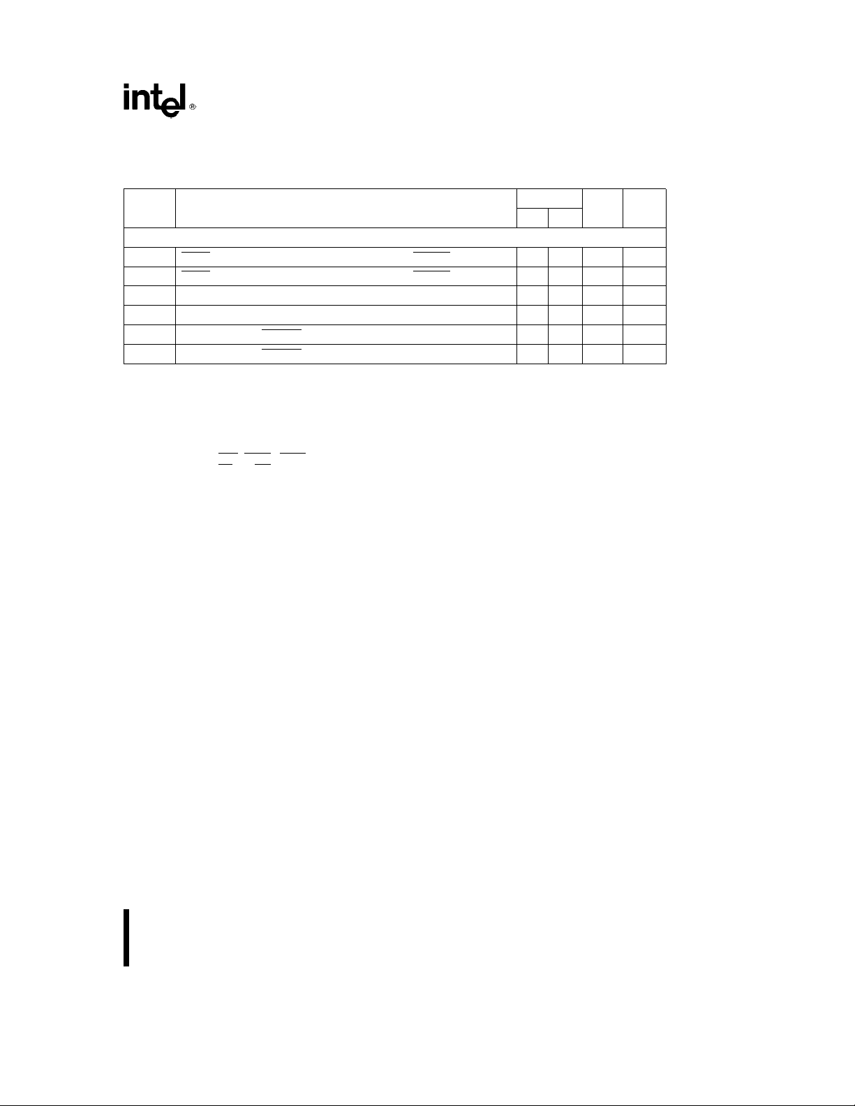
Symbol Parameter
INPUT CLOCK
T
F
T
C
T
CH
T
CL
T
CR
T
CF
CLKIN Frequency 0 50 MHz 1
CLKIN Period 20
CLKIN High Time 8
CLKIN Low Time 8
CLKIN Rise Time 1 7 ns 1, 3
CLKIN Fall Time 1 7 ns 1, 3
OUTPUT CLOCK
T
CD
CLKIN to CLKOUT Delay 0 16 ns 1, 4
T CLKOUT Period 2*T
T
PH
T
PL
T
PR
T
PF
CLKOUT High Time (T/2)b5 (T/2)a5ns 1
CLKOUT Low Time (T/2)b5 (T/2)a5ns 1
CLKOUT Rise Time 1 6 ns 1, 5
CLKOUT Fall Time 1 6 ns 1, 5
OUTPUT DELAYS
T
CHOV1
T
CHOV2
T
CLOV1
T
CLOV2
T
CHOF
T
CLOF
ALE, S2:0, DEN, DT/R, BHE (RFSH), LOCK, A19:16 3 17 ns 1, 4, 6, 7
GCS0:7, LCS, UCS, NCS,RD,WR 3 20 ns 1,4,6,8
BHE (RFSH), DEN, LOCK, RESOUT, HLDA, T0OUT, 3 17 ns 1, 4, 6
T1OUT, A19:16
RD,WR, GCS7:0, LCS, UCS, AD15:0 (AD7:0, A15:8), 3 20 ns 1, 4, 6
NCS
, INTA1:0, S2:0
RD,WR, BHE (RFSH), DT/R, LOCK, S2:0, A19:16 0 20 ns 1
DEN, AD15:0 (AD7:0, A15:8) 0 20 ns 1
25 MHz
Min Max
Units Notes
%
%
%
C
ns 1
ns 1, 2
ns 1, 2
ns 1
28
Page 29
AC SPECIFICATIONS
80C186EB/80C188EB, 80L186EB/80L188EB
AC CharacteristicsÐ80C186EB25
(Continued)
Symbol Parameter
SYNCHRONOUS INPUTS
T
CHIS
T
CHIH
T
CLIS
T
CLIH
T
CLIS
T
CLIH
NOTES:
1. See AC Timing Waveforms, for waveforms and definition.
2. Measure at V
3. Only required to guarantee I
4. Specified for a 50 pF load, see Figure 13 for capacitive derating information.
5. Specified for a 50 pF load, see Figure 14 for rise and fall times outside 50 pF.
6. See Figure 14 for rise and fall times.
7. T
8. T
9. Setup and Hold are required to guarantee recognition.
10. Setup and Hold are required for proper operation.
TEST, NMI, INT4:0, BCLK1:0, T1:0IN, READY, CTS1:0, P2.6, P2.7 10 ns 1, 9
TEST, NMI, INT4:0, BCLK1:0, T1:0IN, READY, CTS1:0 3ns1,9
AD15:0 (AD7:0), READY 10 ns 1, 10
READY, AD15:0 (AD7:0) 3 ns 1, 10
HOLD, PEREQ, ERROR 10 ns 1, 9
HOLD, PEREQ, ERROR 3ns1,9
for high time, VILfor low time.
IH
applies to BHE (RFSH), LOCK and A19:16 only after a HOLD release.
CHOV1
applies to RD and WR only after a HOLD release.
CHOV2
. Maximum limits are bounded by TC,TCHand TCL.
CC
25 MHz
Min Max
Units Notes
29
Page 30
80C186EB/80C188EB, 80L186EB/80L188EB
AC SPECIFICATIONS
AC CharacteristicsÐ80C186EB20/80C186EB13
Symbol Parameter
INPUT CLOCK
T
F
T
C
T
CH
T
CL
T
CR
T
CF
CLKIN Frequency 0 40 0 26 MHz 1
CLKIN Period 25
CLKIN High Time 10
CLKIN Low Time 10
CLKIN Rise Time 1818ns1,3
CLKIN Fall Time 1818ns1,3
OUTPUT CLOCK
T
CD
CLKIN to CLKOUT Delay 0 17 0 23 ns 1, 4
T CLKOUT Period 2*T
T
PH
T
PL
T
PR
T
PF
CLKOUT High Time (T/2)b5 (T/2)a5 (T/2)b5 (T/2)a5ns 1
CLKOUT Low Time (T/2)b5 (T/2)a5 (T/2)b5 (T/2)a5ns 1
CLKOUT Rise Time 1616ns1,5
CLKOUT Fall Time 1616ns1,5
OUTPUT DELAYS
T
CHOV1
ALE, S2:0, DEN, DT/R, 3 22 3 25 ns 1,4,6,7
BHE (RFSH), LOCK,
A19:16
T
CHOV2
T
CLOV1
GCS0:7, LCS, UCS, NCS, 3 27 3 30 ns 1,4,6,8
RD
,WR
BHE (RFSH), DEN, LOCK, 3 22 3 25 ns 1,4,6
RESOUT, HLDA, T0OUT,
T1OUT, A19:16
T
CLOV2
T
CHOF
T
CLOF
RD,WR, GCS7:0, LCS, 3 27 3 30 ns 1,4,6
, AD15:0 (AD7:0,
UCS
A15:8), NCS
, INTA1:0, S2:0
RD,WR, BHE (RFSH), 025025ns1
DT/R
, LOCK, S2:0, A19:16
DEN, AD15:0 (AD7:0, 0 25 0 25 ns 1
A15:8)
20 MHz 13 MHz
Min Max Min Max
%
%
%
Units Notes
2*T
%
%
%
C
ns 1
ns 1, 2
ns 1, 2
ns 1
38.5
12
12
C
30
Page 31

AC SPECIFICATIONS
80C186EB/80C188EB, 80L186EB/80L188EB
AC CharacteristicsÐ80C186EB20/80C186EB13
Symbol Parameter
(Continued)
20 MHz 13 MHz
Min Max Min Max
SYNCHRONOUS INPUTS
T
CHIS
T
CHIH
T
CLIS
T
CLIH
T
CLIS
T
CLIH
NOTES:
1. See AC Timing Waveforms, for waveforms and definition.
2. Measure at V
3. Only required to guarantee I
4. Specified for a 50 pF load, see Figure 13 for capacitive derating information.
5. Specified for a 50 pF load, see Figure 14 for rise and fall times outside 50 pF.
6. See Figure 14 for rise and fall times.
7. T
CHOV1
8. T
CHOV2
9. Setup and Hold are required to guarantee recognition.
10. Setup and Hold are required for proper operation.
TEST, NMI, INT4:0, BCLK1:0, T1:0IN, 10 10 ns 1, 9
READY, CTS1:0
, P2.6, P2.7
TEST, NMI, INT4:0, BCLK1:0, T1:0IN, 3 3 ns 1, 9
READY, CTS1:0
AD15:0 (AD7:0), READY 10 10 ns 1, 10
READY, AD15:0 (AD7:0) 3 3 ns 1, 10
HOLD, PEREQ, ERROR 10 10 ns 1, 9
HOLD, PEREQ, ERROR 3 3 ns 1, 9
for high time, VILfor low time.
IH
applies to BHE (RFSH), LOCK and A19:16 only after a HOLD release.
applies to RD and WR only after a HOLD release.
. Maximum limits are bounded by TC,TCHand TCL.
CC
Units Notes
31
Page 32

80C186EB/80C188EB, 80L186EB/80L188EB
AC SPECIFICATIONS
AC CharacteristicsÐ80L186EB16
Symbol Parameter
INPUT CLOCK
T
F
T
C
T
CH
T
CL
T
CR
T
CF
CLKIN Frequency 0 32 MHz 1
CLKIN Period 31.25
CLKIN High Time 13
CLKIN Low Time 13
CLKIN Rise Time 1 8 ns 1, 3
CLKIN Fall Time 1 8 ns 1, 3
OUTPUT CLOCK
T
CD
CLKIN to CLKOUT Delay 0 30 ns 1, 4
T CLKOUT Period 2*T
T
PH
T
PL
T
PR
T
PF
CLKOUT High Time (T/2)b5 (T/2)a5ns 1
CLKOUT Low Time (T/2)b5 (T/2)a5ns 1
CLKOUT Rise Time 1 9 ns 1, 5
CLKOUT Fall Time 1 9 ns 1, 5
OUTPUT DELAYS
T
CHOV1
T
CHOV2
T
CHOV3
T
CHOV4
T
CHOV5
T
CLOV1
T
CLOV2
T
CHOF
T
CLOF
T
CLOV3
T
CLOV5
DT/R, LOCK, A19:16, R
FSH
GCS0:7, LCS, UCS, NCS,RD,WR 3 27 ns 1,4,6,8
BHE, DEN 325ns1,4
ALE 3 30 ns 1, 4
S2:0 333ns1,4
LOCK, RESOUT, HLDA, T0OUT, T1OUT, A19:16 3 22 ns 1, 4, 6
RD,WR, GCS7:0, LCS, UCS, NCS, INTA1:0, AD15:0 3 27 ns 1, 4, 6
(AD7:0, A15:8)
RD,WR, BHE (RFSH), DT/R, LOCK, S2:0, A19:16 0 25 ns 1
DEN, AD15:0 (AD7:0, A15:8) 0 25 ns 1
BHE, DEN 3 25 ns 1,4,6
S2:0 3 33 ns 1,4,6
16 MHz
Min Max
3 22 ns 1,4,6,7
Units Notes
%
%
%
C
ns 1
ns 1, 2
ns 1, 2
ns 1
32
Page 33

AC SPECIFICATIONS
80C186EB/80C188EB, 80L186EB/80L188EB
AC CharacteristicsÐ80L186EB16
(Continued)
Symbol Parameter
SYNCHRONOUS INPUTS
T
CHIS
T
CHIH
T
CLIS
T
CLIH
T
CLIS
T
CLIH
NOTES:
1. See AC Timing Waveforms, for waveforms and definition.
2. Measure at V
3. Only required to guarantee I
4. Specified for a 50 pF load, see Figure 13 for capacitive derating information.
5. Specified for a 50 pF load, see Figure 14 for rise and fall times outside 50 pF.
6. See Figure 14 for rise and fall times.
7. T
8. T
9. Setup and Hold are required to guarantee recognition.
10. Setup and Hold are required for proper operation.
TEST, NMI, INT4:0, BCLK1:0, T1:0IN, READY, CTS1:0, P2.6, P2.7 15 ns 1, 9
TEST, NMI, INT4:0, T1:0IN, BCLK1:0, READY, CTS1:0 3ns1,9
AD15:0 (AD7:0), READY 15 ns 1, 10
READY, AD15:0 (AD7:0) 3 ns 1, 10
HOLD 15 ns 1, 9
HOLD 3 ns 1, 9
for high time, VILfor low time.
IH
applies to BHE (RFSH), LOCK and A19:16 only after a HOLD release.
CHOV1
applies to RD and WR only after a HOLD release.
CHOV2
. Maximum limits are bounded by TC,TCHand TCL.
CC
16 MHz
Min Max
Units Notes
33
Page 34

80C186EB/80C188EB,80L186EB/80L188EB
ACSPECIFICATIONS
ACCharacteristicsÐ80L186EB13
SymbolParameter
INPUT CLOCK
T
rCLKINFrequency026 MHz1
T
CCLKINPeriod38.5% ns1
T
CHCLKINHighTime15% ns1,2
T
CLCLKINLowTime15% ns1,2
T
CRCLKINRiseTime18 ns1,3
T
CFCLKINFallTime18 ns1,3
OUTPUT CLOCK
T
CDCLKINtoCLKOUTDelay010 ns1,4
T CLKOUT Period 2*T
T
PHCLKOUTHighTime(T/2)b5(T/2)a5
T
PLCLKOUTLowTime(T/2)b5(T/2)a5
T
PRCLKOUTRiseTime110 ns1,5
T
PFCLKOUTFallTime110 ns1,5
OUTPUT DELAYS
T
CHOV1
ALE, S2-0, DEN, DT/R,325 ns1,4,6,7
(RFSH), LOCK,
BHE
A19:16
T
CHOV2
T
CLOV1
GCS0:7, LCS, UCS,330 ns1,4,6,8
,RD,WR
NCS
BHE (RFSH), DEN,325 ns1,4,6
LOCK, RESOUT, HLDA,
T0OUT, T1OUT, A19:16
T
CLOV2
S2:0,RD,WR, GCS7:0,330 ns1,4,6
LCS, UCS, NCS,
, AD15:0 (AD7:0,
INTA1:0
A15:8)
T
CHOF
, BHE (RFSH),030 ns1
RD,WR
DT/R, LOCK, S2:0,
A19:16
T
CLOF
DEN,AD15:0030 ns1
(AD7:0, A15:8)
13MHz8MHz
MinMax No Longer Available
C ns1
UnitsNotes
ns 1
ns 1
34
Page 35

AC SPECIFICATIONS
80C186EB/80C188EB, 80L186EB/80L188EB
AC CharacteristicsÐ80L186EB13/80L186EB8
Symbol Parameter
13 MHz 8 MHz
(Continued)
Units Notes
Min Max Not Available
SYNCHRONOUS INPUTS
T
CHIS
T
CHIH
T
CLISAD15:0(AD7:0),READY20 ns1,10
T
CLIHREADY,AD15:0(AD7:0)3 ns1,10
T
CLISHOLD20 ns1,9
T
CLIHHOLD3 ns1,9
NOTES:
1. See AC Timing Waveforms, for waveforms and definition.
2. Measured at V
3. Only required to guarantee I
4. Specified for a 50 pF load, see Figure 13 for capacitive derating information.
5. Specified for a 50 pF load, see Figure 14 for rise and fall times outside 50 pF.
6. See Figure 14 for rise and fall times.
7. T
CHOV1
8. T
CHOV2
9. Setup and Hold are required to guarantee recognition.
10. Setup and Hold are required for proper operation.
TEST,NMI,INT4:0,20 ns1,9
BCLK1:0, T1:0IN, READY
CTS1:0
, P2.6, P2.7
TEST,NMI,INT4:0,T1:0IN,3 ns1,9
BCLK1:0, READY, CTS1:0
for high time, VILfor low time.
IH
applies to BHE (RFSH), LOCK and A19:16 only after a HOLD release.
applies to RD and WR only after a HOLD release.
. Maximum limits are bounded by TC,TCHand TCL.
CC
35
Page 36
80C186EB/80C188EB, 80L186EB/80L188EB
AC SPECIFICATIONS (Continued)
Relative Timings (80C186EB25, 20, 13/80L186EB16, 13, 8)
Symbol Parameter Min Max Units Notes
RELATIVE TIMINGS
T
LHLL
T
AVLL
T
PLLL
T
LLAX
T
LLWL
T
LLRL
T
WHLH
T
AFRL
T
RLRH
T
WLWH
T
RHAV
T
WHDX
T
WHPH
T
RHPH
T
PHPL
T
OVRH
T
RHOX
NOTES:
1. Assumes equal loading on both pins.
2. Can be extended using wait states.
3. Not tested
ALE Rising to ALE Falling Tb15 ns
Address Valid to ALE Falling (/2Tb10 ns
Chip Selects Valid to ALE Falling (/2Tb10 ns 1
Address Hold from ALE Falling (/2Tb10 ns
ALE Falling to WR Falling (/2Tb15 ns 1
ALE Falling to RD Falling (/2Tb15 ns 1
WR Rising to ALE Rising (/2Tb10 ns 1
Address Float to RD Falling 0 ns
RD Falling to RD Rising (2*T)b5ns2
WR Falling to WR Rising (2*T)b5ns2
RD Rising to Address Active Tb15 ns
Output Data Hold after WR Rising Tb15 ns
WR Rising to Chip Select Rising (/2Tb10 ns 1
RD Rising to Chip Select Rising (/2Tb10 ns 1
CS Inactive to CS Active (/2Tb10 ns 1
ONCE Active to RESIN Rising T ns 3
ONCE Hold from RESIN Rising T ns 3
36
Page 37
80C186EB/80C188EB, 80L186EB/80L188EB
AC SPECIFICATIONS (Continued)
Serial Port Mode 0 Timings (80C186EB25, 20, 13/80L186EB16, 13, 8)
Symbol Parameter Min Max Unit Notes
T
T
T
T
T
T
T
T
T
T
T
T
NOTES:
1. See Figure 12 for waveforms.
2. n is the value of the BxCMP register ignoring the ICLK Bit (i.e., ICLK
TXD Clock Period T (na1) ns 1, 2
XLXL
TXD Clock Low to Clock High (nl1) 2Tb35 2Ta35 ns 1
XLXH
TXD Clock Low to Clock High (ne1) Tb35 Ta35 ns 1
XLXH
TXD Clock High to Clock Low (nl1) (nb1) Tb35 (nb1) Ta35 ns 1, 2
XHXL
TXD Clock High to Clock Low (ne1) Tb35 Ta35 ns 1
XHXL
RXD Output Data Setup to TXD Clock High (nl1) (nb1) Tb35 ns 1, 2
QVXH
RXD Output Data Setup to TXD Clock High (ne1) Tb35 ns 1
QVXH
RXD Output Data Hold after TXD Clock High (nl1) 2Tb35 ns 1
XHQX
RXD Output Data Hold after TXD Clock High (ne1) Tb35 ns 1
XHQX
RXD Output Data Float after Last TXD Clock High Ta20 ns 1
XHQZ
RXD Input Data Setup to TXD Clock High Ta20 ns 1
DVXH
RXD Input Data Hold after TXD Clock High 0 ns 1
XHDX
e
0).
37
Page 38
80C186EB/80C188EB, 80L186EB/80L188EB
AC TEST CONDITIONS
The AC specifications are tested with the 50 pF load
shown in Figure 7. See the Derating Curves section
to see how timings vary with load capacitance.
Specifications are measured at the V
point, unless otherwise specified. See AC Timing
/2 crossing
CC
Waveforms, for AC specification definitions, test
pins, and illustrations.
AC TIMING WAVEFORMS
Figure 8. Input and Output Clock Waveform
e
C
50 pF for all signals.
L
272433– 8
Figure 7. AC Test Load
272433– 9
38
Page 39

NOTE:
20% V
k
Floatk80% V
CC
80C186EB/80C188EB, 80L186EB/80L188EB
272433– 10
CC
Figure 9. Output Delay and Float Waveform
Figure 10. Input Setup and Hold
272433– 11
39
Page 40

80C186EB/80C188EB, 80L186EB/80L188EB
NOTE:
Pin names in parentheses apply to 80C188EB/80L188EB
Figure 11. Relative Signal Waveform
Figure 12. Serial Port Mode 0 Waveform
40
272433– 12
272433– 13
Page 41

80C186EB/80C188EB, 80L186EB/80L188EB
DERATING CURVES
TYPICAL OUTPUT DELAY VARIATIONS VERSUS LOAD CAPACITANCE
Figure 13
TYPICAL RISE AND FALL VARIATIONS VERSUS LOAD CAPACITANCE
272433– 14
Figure 14
272433– 15
41
Page 42

80C186EB/80C188EB, 80L186EB/80L188EB
RESET
The processor will perform a reset operation any
time the RESIN
synchronized before it is presented internally, which
means that the clock must be operating before a
reset can take effect. From a power-on state, RESIN
must be held active (low) in order to guarantee correct initialization of the processor. Failure to pro-
vide RESIN
result in unspecified operation of the device.
Figure 14 shows the correct reset sequence when
first applying power to the processor. An external
clock connected to CLKIN must not exceed the V
threshold being applied to the processor. This is normally not a problem if the clock driver is supplied
with the same V
When attaching a crystal to the device, RESIN
remain active until both V
(the length of time is application specific and depends on the startup characteristics of the crystal
pin active. The RESIN pin is actually
while the device is powering up will
CC
that supplies the processor.
CC
and CLKOUT are stable
CC
must
circuit). The RESIN
pin is designed to operate correctly using an RC reset circuit, but the designer
must ensure that the ramp time for V
long that RESIN
low level when V
conditions.
is never really sampled at a logic
reaches minimum operating
CC
is not so
CC
Figure 16 shows the timing sequence when RESIN
is applied after VCCis stable and the device has
been operating. Note that a reset will terminate all
activity and return the processor to a known operating state. Any bus operation that is in progress at the
time RESIN
is asserted will terminate immediately
(note that most control signals will be driven to their
inactive state first before floating).
While RESIN is active, bus signals LOCK, A19/
ONCE
, and A18:16 are configured as inputs and
weakly held high by internal pullup transistors. Only
19/ONCE
enable ONCE
any time while RESIN
can be overdriven to a low and is used to
Mode. Forcing LOCK or A18:16 low at
is low is prohibited and will
cause unspecified device operation.
42
Page 43

80C186EB/80C188EB, 80L186EB/80L188EB
272433– 16
Figure 15. Cold Reset Waveforms
. If RESIN is sampled high while CLKOUT is high (solid line), then CLKOUT will remain
is sampled high while CLKOUT is low (dashed line), then CLKOUT will not be affected.
NOTE:
CLKOUT synchronization occurs on the rising edge of RESIN
Pin names in parentheses apply to 80C188EB/80L188EB
low for two CLKIN periods. If RESIN
43
Page 44

80C186EB/80C188EB, 80L186EB/80L188EB
272433– 17
44
Figure 16. Warm Reset Waveforms
. If RESIN is sampled high while CLKOUT is high (solid line), then CLKOUT will remain
is sampled high while CLKOUT is low (dashed line), then CLKOUT will not be affected.
NOTE:
CLKOUT synchronization occurs on the rising edge of RESIN
Pin names in parentheses apply to 80C188EB/80L188EB
low for two CLKIN periods. If RESIN
Page 45

80C186EB/80C188EB, 80L186EB/80L188EB
BUS CYCLE WAVEFORMS
Figures 17 through 23 present the various bus cycles that are generated by the processor. What is
shown in the figure is the relationship of the various
bus signals to CLKOUT. These figures along with
the information present in AC Specifications allow
the user to determine all the critical timing analysis
needed for a given application.
NOTE:
Pin names in parentheses apply to 80C188EB/80L188EB
Figure 17. Read, Fetch, and Refresh Cycle Waveforms
272433– 18
45
Page 46
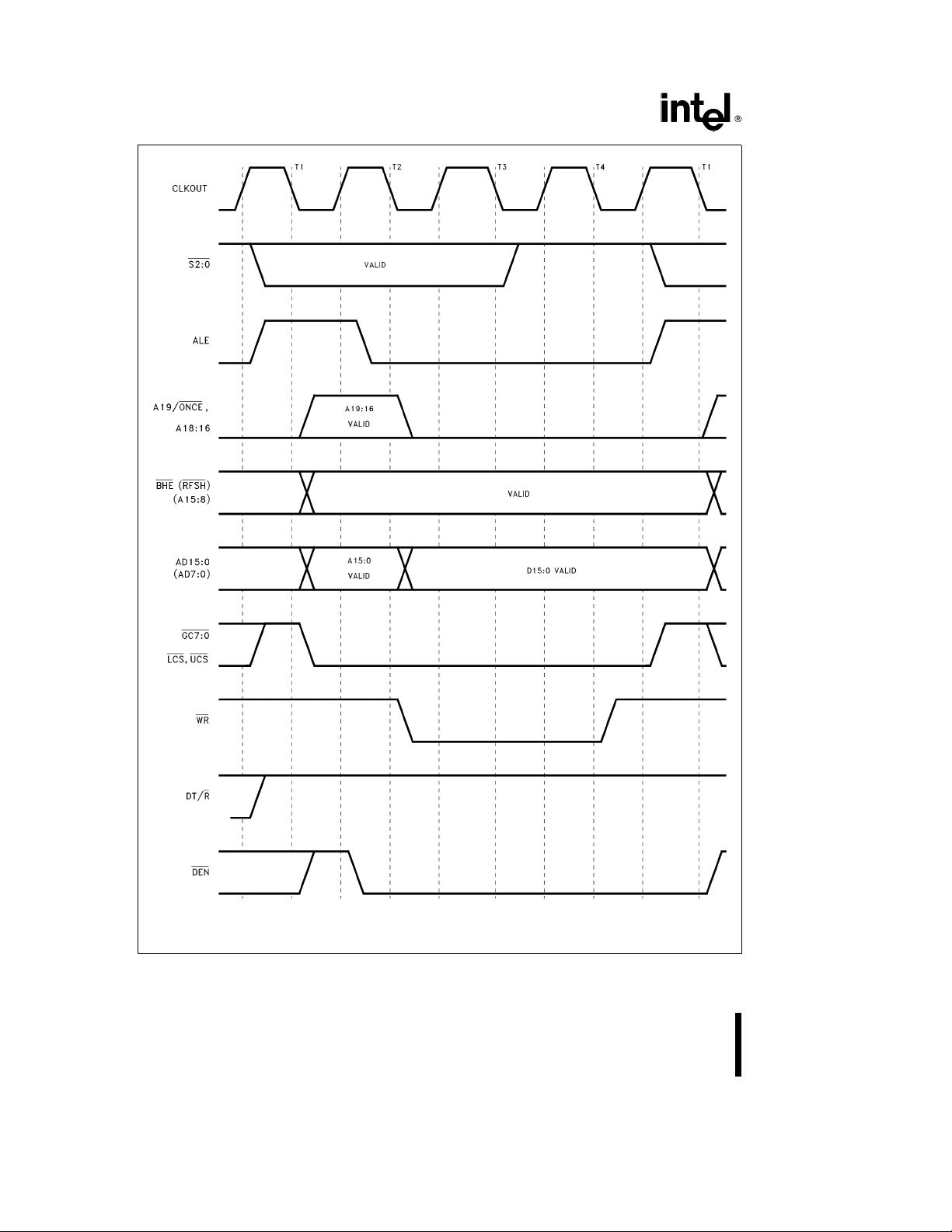
80C186EB/80C188EB, 80L186EB/80L188EB
NOTE:
Pin names in parentheses apply to 80C188EB/80L188EB
Figure 18. Write Cycle Waveforms
46
272433– 19
Page 47
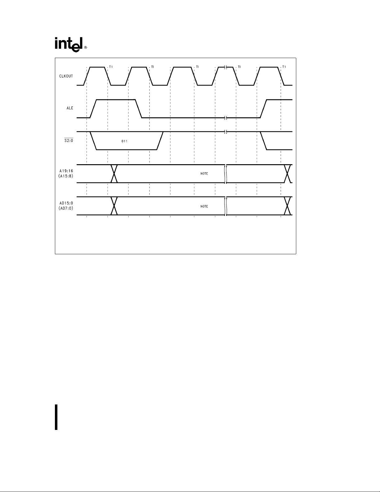
80C186EB/80C188EB, 80L186EB/80L188EB
272433– 20
NOTE:
The address driven is typically the location of the next instruction prefetch. Under a majority of instruction sequences the
AD15:0 (AD7:0) bus will float, while the A19:16 (A19:8) bus remains driven and all bus control signals are driven to their
inactive state.
Pin names in parentheses apply to 80C188EB/80L188EB
Figure 19. Halt Cycle Waveforms
47
Page 48

80C186EB/80C188EB, 80L186EB/80L188EB
NOTE:
Pin names in parentheses apply to 80C188EB/80L188EB
Figure 20. Interrupt Acknowledge Cycle Waveform
48
272433– 21
Page 49
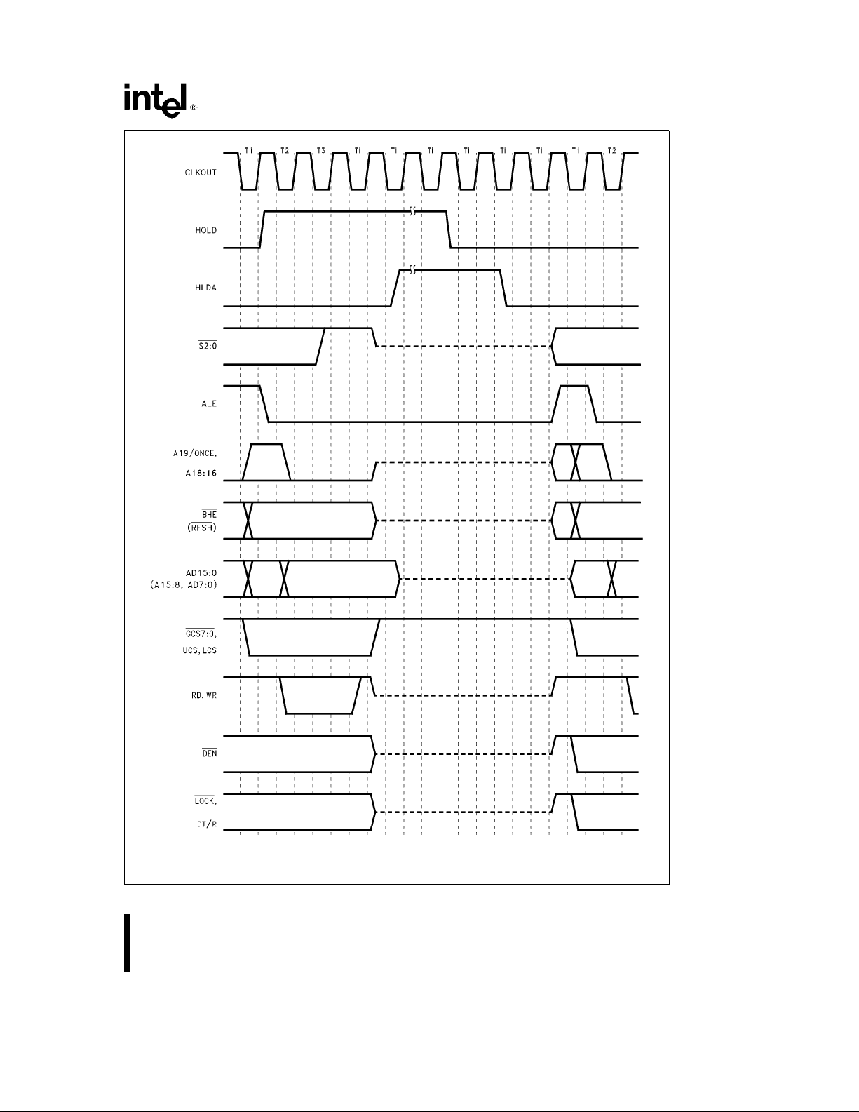
80C186EB/80C188EB, 80L186EB/80L188EB
NOTE:
Pin names in parentheses apply to 80C188EB/80L188EB
Figure 21. HOLD/HLDA Waveforms
272433– 22
49
Page 50

80C186EB/80C188EB, 80L186EB/80L188EB
NOTES:
1. READY
2. Lighter lines indicate READ cycles, darker lines indicate WRITE cycles.
Pin names in parentheses apply to 80C188EB/80L188EB
must be low by either edge to cause a wait state.
Figure 22. Refresh during Hold Acknowledge
50
272433– 23
Page 51

80C186EB/80C188EB, 80L186EB/80L188EB
NOTES:
1. READY
2. Lighter lines indicate READ cycles, darker lines indicate WRITE cycles.
Pin names in parentheses apply to 80C188EB/80L188EB
must be low by either edge to cause a wait state.
Figure 23. Ready Waveforms
272433– 24
51
Page 52

80C186EB/80C188EB, 80L186EB/80L188EB
EXECUTION TIMINGS
A determination of program execution timing must
consider the bus cycles necessary to prefetch instructions as well as the number of execution unit
cycles necessary to execute instructions. The following instruction timings represent the minimum
execution time in clock cycles for each instruction.
The timings given are based on the following assumptions:
The opcode, along with any data or displacement
#
required for execution of a particular instruction,
has been prefetched and resides in the queue at
the time it is needed.
No wait states or bus HOLDs occur.
#
All word-data is located on even-address bound-
#
aries (80C186EB only).
All jumps and calls include the time required to fetch
the opcode of the next instruction at the destination
address.
All instructions which involve memory accesses can
require one or two additional clocks above the minimum timings shown due to the asynchronous handshake between the bus interface unit (BIU) and execution unit.
With a 16-bit BIU, the 80C186EB has sufficient bus
performance to ensure that an adequate number of
prefetched bytes will reside in the queue (6 bytes)
most of the time. Therefore, actual program execution time will not be substantially greater than that
derived from adding the instruction timings shown.
The 80C188EB 8-bit BIU is limited in its performance
relative to the execution unit. A sufficient number of
prefetched bytes may not reside in the prefetch
queue (4 bytes) much of the time. Therefore, actual
program execution time will be substantially greater
than that derived from adding the instruction timings
shown.
52
Page 53

80C186EB/80C188EB, 80L186EB/80L188EB
INSTRUCTION SET SUMMARY
Function Format Clock Clock Comments
DATA TRANSFER
e
Move:
MOV
Register to Register/Memory 1000100w modreg r/m 2/12 2/12*
Register/memory to register 1000101w modreg r/m 2/9 2/9*
Immediate to register/memory 1100011w mod000 r/m data data if we1 12/13 12/13 8/16-bit
Immediate to register 1011w reg data data if we1 3/4 3/4 8/16-bit
Memory to accumulator 1010000w addr-low addr-high 8 8*
Accumulator to memory 1010001w addr-low addr-high 9 9*
Register/memory to segment register 10001110 mod0reg r/m 2/9 2/13
Segment register to register/memory 10001100 mod0reg r/m 2/11 2/15
PUSHePush:
Memory 11111111 mod110 r/m 16 20
Register 01010 reg 10 14
Segment register 000reg110 9 13
Immediate 011010s0 data data if se01014
PUSHAePush All 01100000 36 68
POPePop:
Memory 10001111 mod000 r/m 20 24
Register 01011 reg 10 14
Segment register 000reg111 (regi01) 8 12
POPAePopAll 01100001 51 83
XCHGeExchange:
Register/memory with register 1000011w modreg r/m 4/17 4/17*
Register with accumulator 10010 reg 3 3
INeInput from:
Fixed port 1110010w port 10 10*
Variable port 1110110w 8 8*
OUTeOutput to:
Fixed port 1110011w port 9 9*
Variable port 1110111w 7 7*
XLATeTranslate byte to AL 11010111 11 15
LEAeLoad EA to register 10001101 modreg r/m 6 6
LDSeLoad pointer to DS 11000101 modreg r/m (modi11) 18 26
LESeLoad pointer to ES 11000100 modreg r/m (modi11) 18 26
LAHFeLoad AH with flags 10011111 2 2
SAHFeStore AH into flags 10011110 3 3
PUSHFePush flags 10011100 9 13
POPFePop flags 10011101 8 12
Shaded areas indicate instructions not available in 8086/8088 microsystems.
NOTE:
*Clock cycles shown for byte transfers. For word operations, add 4 clock cycles for all memory transfers.
80C186EB 80C188EB
Cycles Cycles
53
Page 54
80C186EB/80C188EB, 80L186EB/80L188EB
INSTRUCTION SET SUMMARY (Continued)
Function Format Clock Clock Comments
DATA TRANSFER (Continued)
e
SEGMENT
CS 00101110 2 2
SS 00110110 2 2
DS 00111110 2 2
ES 00100110 2 2
ARITHMETIC
ADD
Reg/memory with register to either 000000dw modreg r/m 3/10 3/10*
Immediate to register/memory 100000sw mod000 r/m data data if s we01 4/16 4/16*
Immediate to accumulator 0000010w data data if we1 3/4 3/4 8/16-bit
ADCeAdd with carry:
Reg/memory with register to either 000100dw modreg r/m 3/10 3/10*
Immediate to register/memory 100000sw mod010 r/m data data if s we01 4/16 4/16*
Immediate to accumulator 0001010w data data if we1 3/4 3/4 8/16-bit
INCeIncrement:
Register/memory 1111111w mod000 r/m 3/15 3/15*
Register 01000 reg 3 3
SUBeSubtract:
Reg/memory and register to either 001010dw modreg r/m 3/10 3/10*
Immediate from register/memory 100000sw mod101 r/m data data if s we01 4/16 4/16*
Immediate from accumulator 0010110w data data if we1 3/4 3/4 8/16-bit
SBBeSubtract with borrow:
Reg/memory and register to either 000110dw modreg r/m 3/10 3/10*
Immediate from register/memory 100000sw mod011 r/m data data if s we01 4/16 4/16*
Immediate from accumulator 0001110w data data if we1 3/4 3/4* 8/16-bit
DECeDecrement
Register/memory 1111111w mod001 r/m 3/15 3/15*
Register 01001 reg 3 3
CMPeCompare:
Register/memory with register 0011101w modreg r/m 3/10 3/10*
Register with register/memory 0011100w modreg r/m 3/10 3/10*
Immediate with register/memory 100000sw mod111 r/m data data if s we01 3/10 3/10*
Immediate with accumulator 0011110w data data if we1 3/4 3/4 8/16-bit
NEGeChange sign register/memory 1111011w mod011 r/m 3/10 3/10*
AAAeASCII adjust for add 00110111 8 8
DAAeDecimal adjust for add 00100111 4 4
AASeASCII adjust for subtract 00111111 7 7
DASeDecimal adjust for subtract 00101111 4 4
MULeMultiply (unsigned): 1111011w mod100 r/m
Register-Byte 26–28 26–28
Register-Word 35–37 35–37
Memory-Byte 32–34 32–34
Memory-Word 41–43 41–43*
e
Add:
Segment Override:
Shaded areas indicate instructions not available in 8086/8088 microsystems.
NOTE:
*Clock cycles shown for byte transfers. For word operations, add 4 clock cycles for all memory transfers.
54
80C186EB 80C188EB
Cycles Cycles
Page 55

80C186EB/80C188EB, 80L186EB/80L188EB
INSTRUCTION SET SUMMARY (Continued)
Function Format Clock Clock Comments
ARITHMETIC (Continued)
IMULeInteger multiply (signed): 1111011w mod101 r/m
Register-Byte 25–28 25–28
Register-Word 34–37 34–37
Memory-Byte 31–34 31–34
Memory-Word 40–43 40–43*
IMULeInteger Immediate multiply 011010s1 modreg r/m data data if se0 22– 25/ 22– 25/
(signed)
DIVeDivide (unsigned): 1111011w mod110 r/m
Register-Byte 29 29
Register-Word 38 38
Memory-Byte 35 35
Memory-Word 44 44*
IDIVeInteger divide (signed): 1111011w mod111 r/m
Register-Byte 44–52 44–52
Register-Word 53–61 53–61
Memory-Byte 50–58 50–58
Memory-Word 59–67 59–67*
AAMeASCII adjust for multiply 11010100 00001010 19 19
AADeASCII adjust for divide 11010101 00001010 15 15
CBWeConvert byte to word 10011000 2 2
CWDeConvert word to double word 10011001 4 4
LOGIC
Shift/Rotate Instructions:
Register/Memory by 1 1101000w modTTTr/m 2/15 2/15
Register/Memory by CL 1101001w modTTTr/m
Register/Memory by Count 1100000w modTTTr/m count
TTT Instruction
000 ROL
001 ROR
010 RCL
011 RCR
1 0 0 SHL/SAL
101 SHR
e
AND
And:
Reg/memory and register to either 001000dw modreg r/m 3/10 3/10*
Immediate to register/memory 1000000w mod100 r/m data data if we1 4/16 4/16*
Immediate to accumulator 0010010w data data if we1 3/4 3/4* 8/16-bit
TESTeAnd function to flags, no result:
Register/memory and register 1000010w modreg r/m 3/10 3/10*
Immediate data and register/memory 1111011w mod000 r/m data data if we1 4/10 4/10*
Immediate data and accumulator 1010100w data data if we1 3/4 3/4 8/16-bit
OReOr:
Reg/memory and register to either 000010dw modreg r/m 3/10 3/10*
Immediate to register/memory 1000000w mod001 r/m data data if we1 4/16 4/16*
Immediate to accumulator 0000110w data data if we1 3/4 3/4* 8/16-bit
111 SAR
Shaded areas indicate instructions not available in 8086/8088 microsystems.
NOTE:
*Clock cycles shown for byte transfers. For word operations, add 4 clock cycles for all memory transfers.
80C186EB 80C188EB
Cycles Cycles
29–32 29–32
5an/17an5an/17an
5an/17an5an/17an
55
Page 56

80C186EB/80C188EB, 80L186EB/80L188EB
INSTRUCTION SET SUMMARY (Continued)
Function Format Clock Clock Comments
LOGIC (Continued)
e
Exclusive or:
XOR
Reg/memory and register to either 001100dw modreg r/m 3/10 3/10*
Immediate to register/memory 1000000w mod110 r/m data data if we1 4/16 4/16*
Immediate to accumulator 0011010w data data if we1 3/4 3/4 8/16-bit
NOTeInvert register/memory 1111011w mod010 r/m 3/10 3/10*
STRING MANIPULATION
MOVSeMove byte/word 1010010w 14 14*
CMPSeCompare byte/word 1010011w 22 22*
SCASeScan byte/word 1010111w 15 15*
LODSeLoad byte/wd to AL/AX 1010110w 12 12*
STOSeStore byte/wd from AL/AX 1010101w 10 10*
INSeInput byte/wd from DX port 0110110w 14 14
OUTSeOutput byte/wd to DX port 0110111w 14 14
Repeated by count in CX (REP/REPE/REPZ/REPNE/REPNZ)
MOVSeMove string 11110010 1010010w 8a8n 8a8n*
CMPSeCompare string 1111001z 1010011w 5a22n 5a22n*
SCASeScan string 1111001z 1010111w 5a15n 5a15n*
LODSeLoad string 11110010 1010110w 6a11n 6a11n*
STOSeStore string 11110010 1010101w 6a9n 6a9n*
INSeInput string 11110010 0110110w 8a8n 8a8n*
OUTSeOutput string 11110010 0110111w 8a8n 8a8n*
CONTROL TRANSFER
e
CALL
Call:
Direct within segment 11101000 disp-low disp-high 15 19
Register/memory 11111111 mod010 r/m 13/19 17/27
indirect within segment
Direct intersegment 10011010 segment offset 23 31
segment selector
Indirect intersegment 11111111 mod011 r/m (modi11) 38 54
JMPeUnconditional jump:
Short/long 11101011 disp-low 14 14
Direct within segment 11101001 disp-low disp-high 14 14
Register/memory 11111111 mod100 r/m 11/17 11/21
indirect within segment
Direct intersegment 11101010 segment offset 14 14
segment selector
Indirect intersegment 11111111 mod101 r/m (modi11) 26 34
Shaded areas indicate instructions not available in 8086/8088 microsystems.
NOTE:
*Clock cycles shown for byte transfers. For word operations, add 4 clock cycles for all memory transfers.
80C186EB 80C188EB
Cycles Cycles
56
Page 57

80C186EB/80C188EB, 80L186EB/80L188EB
INSTRUCTION SET SUMMARY (Continued)
Function Format Clock Clock Comments
CONTROL TRANSFER (Continued)
e
Return from CALL:
RET
Within segment 11000011 16 20
Within seg adding immed to SP 11000010 data-low data-high 18 22
Intersegment 11001011 22 30
Intersegment adding immediate to SP 11001010 data-low data-high 25 33
JE/JZeJump on equal/zero 01110100 disp 4/13 4/13 JMP not
JL/JNGEeJump on less/not greater or equal 01111100 disp 4/13 4/13
JLE/JNGeJump on less or equal/not greater 01111110 disp 4/13 4/13
JB/JNAEeJump on below/not above or equal 01110010 disp 4/13 4/13
JBE/JNAeJump on below or equal/not above 01110110 disp 4/13 4/13
JP/JPEeJump on parity/parity even 01111010 disp 4/13 4/13
JOeJump on overflow 01110 000 disp 4/13 4/13
JSeJump on sign 01111000 disp 4/13 4/13
JNE/JNZeJump on not equal/not zero 01110101 disp 4/13 4/13
JNL/JGEeJump on not less/greater or equal 01111101 disp 4/13 4/13
JNLE/JGeJump on not less or equal/greater 01111111 disp 4/13 4/13
JNB/JAEeJump on not below/above or equal 01110011 disp 4/13 4/13
JNBE/JAeJump on not below or equal/above 01110111 disp 4/13 4/13
JNP/JPOeJump on not par/par odd 01111011 disp 4/13 4/13
JNOeJump on not overflow 01110001 disp 4/13 4/13
JNSeJump on not sign 01111001 disp 4/13 4/13
JCXZeJump on CX zero 11100011 disp 5/15 5/15
LOOPeLoop CX times 11100010 disp 6/16 6/16 LOOP not
LOOPZ/LOOPEeLoop while zero/equal 11100001 disp 6/16 6/16
LOOPNZ/LOOPNEeLoop while not zero/equal 11100000 disp 6/16 6/16
ENTEReEnter Procedure 11001000 data-low data-high L
Le0 15 19
e
1 25 29
L
l
1
L
LEAVEeLeave Procedure 11001001 8 8
INTeInterrupt:
Type specified 11001101 type 47 47
Type 3 11001100 45 45 ifINT. taken/
INTOeInterrupt on overflow 11001110 48/4 48/4
80C186EB 80C188EB
Cycles Cycles
22a16(nb1) 26a20(nb1)
taken/JMP
taken
taken/LOOP
taken
if INT. not
taken
IRETeInterrupt return 11001111 28 28
BOUNDeDetect value out of range 01100010 modreg r/m 33–35 33–35
Shaded areas indicate instructions not available in 8086/8088 microsystems.
NOTE:
*Clock cycles shown for byte transfers. For word operations, add 4 clock cycles for all memory transfers.
57
Page 58
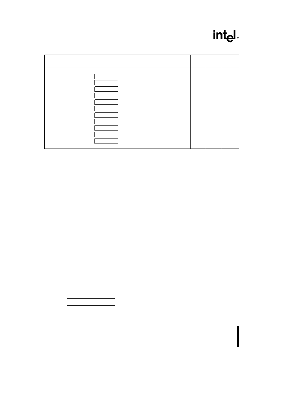
80C186EB/80C188EB, 80L186EB/80L188EB
INSTRUCTION SET SUMMARY (Continued)
Function Format Clock Clock Comments
PROCESSOR CONTROL
CLCeClear carry 11111000 2 2
CMCeComplement carry 11110101 2 2
STCeSet carry 11111001 2 2
CLDeClear direction 11111100 2 2
STDeSet direction 11111101 2 2
CLIeClear interrupt 11111010 2 2
STIeSet interrupt 11111011 2 2
HLTeHalt 11110100 2 2
WAITeWait 10011011 6 6 ifTESTe0
LOCKeBus lock prefix 11110000 2 2
NOPeNo Operation 10010000 3 3
Shaded areas indicate instructions not available in 8086/8088 microsystems.
NOTE:
*Clock cycles shown for byte transfers. For word operations, add 4 clock cycles for all memory transfers.
(TTT LLL are opcode to processor extension)
80C186EB 80C188EB
Cycles Cycles
FOOTNOTES
The Effective Address (EA) of the memory operand
is computed according to the mod and r/m fields:
if mod
if mod
if mod
if mod
if r/m
if r/m
if r/m
if r/m
if r/m
if r/m
if r/m
if r/m
DISP follows 2nd byte of instruction (before data if
required)
*except if mod
disp-high: disp-low.
EA calculation time is 4 clock cycles for all modes,
and is included in the execution times given whenever appropriate.
e
11 then r/m is treated as a REG field
e
00 then DISPe0*, disp-low and disphigh are absent
e
01 then DISPedisp-low sign-extended to 16-bits, disp-high is absent
e
10 then DISPedisp-high: disp-low
e
000 then EAe(BX)a(SI)aDISP
e
001 then EAe(BX)a(DI)aDISP
e
010 then EAe(BP)a(SI)aDISP
e
011 then EAe(BP)a(DI)aDISP
e
100 then EAe(SI)aDISP
e
101 then EAe(DI)aDISP
e
110 then EAe(BP)aDISP*
e
111 then EAe(BX)aDISP
e
00 and r/me110 then EA
Segment Override Prefix
0 0 1 reg 1 1 0
reg is assigned according to the following:
Segment
reg Register
00 ES
01 CS
10 SS
11 DS
REG is assigned according to the following table:
16-Bit (w
e
1) 8-Bit (we0)
000 AX 000 AL
001 CX 001 CL
010 DX 010 DL
011 BX 011 BL
100 SP 100 AH
101 BP 101 CH
110 SI 110 DH
111 DI 111 BH
The physical addresses of all operands addressed
e
by the BP register are computed using the SS segment register. The physical addresses of the destination operands of the string primitive operations
(those addressed by the DI register) are computed
using the ES segment, which may not be overridden.
58
Page 59

80C186EB/80C188EB, 80L186EB/80L188EB
ERRATA
An 80C186EB/80L186EB with a STEPID value of
0001H has the following known errata. A device with
a STEPID of 0001H can be visually identified by the
presence of an ‘‘A’’ alpha character next to the
FPO number. The FPO number location is shown in
Figures 4, 5 and 6.
1. A19/ONCE
RESIN
all times to remain in the ONCE Mode. Removing
A19/ONCE
put pins to a driving state, however, the
80C186EB will remain in a reset state.
2. During interrupt acknowledge (INTA) bus cycles,
the bus controller will ignore the state of the
READY pin if the previous bus cycle ignored the
state of the READY pin. This errata can only occur if the Chip-Select Unit is being used. All active
chip-selects must be programmed to use READY
(RDY bit must be programmed to a 1) if waitstates are required for INTA bus cycles.
3. CLKOUT will transition off the rising edge of
CLKIN rather than the falling edge of CLKIN. This
does not affect any bus timings other than T
4. RESIN has a hysterisis of only 130 mV. It is recommended that RESIN
triggered device to avoid processor lockup during
reset using an RC circuit.
is not latched by the rising edge of
. A19/ONCE must remain active (LOW) at
after RESIN is high will return all out-
CD
be driven by a Schmitt
5. SINT1 will only go active for one clock period
when a receive or transmit interrupt is pending
(i.e., it does not remain active until the S1STS
register is read). If SINT1 is to be connected to
any of the processor interrupt lines (INT0– INT4),
then it must be latched by user logic.
An 80C186EB/80L186EB with a STEPID value of
0001H or 0002H has the following known errata. A
device with a STEPID of 0002H can be visually identified by noting the presence of a ‘‘B’’, ‘‘C’’, ‘‘D’’, or
‘‘E’’ alpha character next to the FPO number. The
FPO number location is shown in Figures 4, 5 and 6.
1. An internal condition with the interrupt controller
can cause no acknowledge cycle on the INTA1
line in response to INT1. This errata only occurs
when Interrupt 1 is configured in cascade mode
and a higher priority interrupt exists. This errata
will not occur consistantly, it is dependent on interrupt timing.
REVISION HISTORY
This data sheet replaces the following data sheets:
.
270803-004 80C186EB
270885-003 80C188EB
270921-003 80L186EB
270920-003 80L188EB
272311-001 SB80C188EB/SB80L188EB
272312-001 SB80C186EB/SB80L186EB
59
Page 60

Copyright © Each Manufacturing Company.
All Datasheets cannot be modified without permission.
This datasheet has been download from :
www.AllDataSheet.com
100% Free DataSheet Search Site.
Free Download.
No Register.
Fast Search System.
www.AllDataSheet.com
 Loading...