

Page 1

80C196KB
数控原理与维修 http://www.agreenleaf.cn
User’s Guide
November 1990
Order Number: 270651-003
Page 2

Information in this document is provided in connection with Intel products. No license, express or implied, by estoppel or
数控原理与维修 http://www.agreenleaf.cn
otherwise, to any intellectual property rights is granted by this document. Except as provided in Intel’s Terms and Conditions of
Sale for such products, Intel assumes no liability whatsoever, and Intel disclaims any express or implied warranty, relating to
sale and/or use of Intel products including liability or warranties relating to fitness for a particular purpose, merchantability, or
infringement of any patent, copyright or other intellectual property right. Intel products are not intended for use in medical, life
saving, or life sustaining applications.
Intel may make changes to specifications and product descriptions at any time, without notice.
*Third-party brands and names are the property of their respective owners.
Contact your local Intel sales office or your distributor to obtain the latest specifications and before placing your product order.
Copies of documents which have an ordering number and are referenced in this document, or other Intel literature, may be
obtained from:
Intel Corporation
P.O. Box 7641
Mt. Prospect, IL 60056-7641
or call 1-800-879-4683
COPYRIGHT©INTEL CORPORATION, 1996
Page 3

80C196KB USER’S GUIDE
数控原理与维修 http://www.agreenleaf.cn
CONTENTS PAGE
1.0 CPU OPERATION
1.1 Memory Controller ААААААААААААААААААА 2
1.2 CPU Control ААААААААААААААААААААААААА 2
1.3 Internal Timing АААААААААААААААААААААА 2
2.0 MEMORY SPACE АААААААААААААААААААААА 4
2.1 Register File ААААААААААААААААААААААААА 4
2.2 Special Function Registers АААААААААА 4
2.3 Reserved Memory Spaces ААААААААААА 8
2.4 Internal ROM and EPROM ААААААААААА 8
2.5 System Bus ААААААААААААААААААААААААА 9
3.0 SOFTWARE OVERVIEW АААААААААААААА 9
3.1 Operand Types АААААААААААААААААААААА 9
3.2 Operand Addressing АААААААААААААААА 10
3.3 Program Status Word ААААААААААААААА 12
3.4 Instruction Set АААААААААААААААААААААА 14
3.5 80C196KB Instruction Set
Additions and Differences
3.6 Software Standards and
Conventions ААААААААААААААААААААААААА 22
3.7 Software Protection Hints ААААААААААА 23
4.0 PERIPHERAL OVERVIEW АААААААААААА 23
4.1 Pulse Width Modulation Output
(D/A) АААААААААААААААААААААААААААААААА 24
4.2 Timers ААААААААААААААААААААААААААААА 24
4.3 High Speed Inputs (HSI) АААААААААААА 24
4.4 High Speed Outputs (HSO) ААААААААА 24
4.5 Serial Port АААААААААААААААААААААААААА 24
4.6 A/D Converter ААААААААААААААААААААА 26
4.7 I/O Ports ААААААААААААААААААААААААААА 26
4.8 Watchdog Timer АААААААААААААААААААА 26
5.0 INTERRUPTS ААААААААААААААААААААААААА 27
5.1 Interrupt Control АААААААААААААААААААА 29
5.2 Interrupt Priorities АААААААААААААААААА 29
5.3 Critical Regions АААААААААААААААААААА 31
5.4 Interrupt Timing АААААААААААААААААААА 31
5.5 Interrupt Summary АААААААААААААААААА 32
ААААААААААААААААААААА 1
АААААААААААА 22
CONTENTS PAGE
6.0 Pulse Width Modulation Output
(D/A)
ААААААААААААААААААААААААААААААААААА 33
6.1 Analog Outputs ААААААААААААААААААААА 35
7.0 TIMERS АААААААААААААААААААААААААААААА 36
7.1 Timer1 ААААААААААААААААААААААААААААА 36
7.2 Timer2 ААААААААААААААААААААААААААААА 36
7.3 Sampling on External Timer
Pins ААААААААААААААААААААААААААААААААА 36
7.4 Timer Interrupts АААААААААААААААААААА 37
8.0 HIGH SPEED INPUTS АААААААААААААААА 38
8.1 HSI Modes ААААААААААААААААААААААААА 39
8.2 HSI Status ААААААААААААААААААААААААА 39
8.3 HSI Interrupts АААААААААААААААААААААА 40
8.4 HSI Input Sampling ААААААААААААААААА 40
8.5 Initializing the HSI АААААААААААААААААА 40
9.0 HIGH SPEED OUTPUTS АААААААААААААА 40
9.1 HSO Interrupts and Software
Timers ААААААААААААААААААААААААААААААА 41
9.2 HSO CAM АААААААААААААААААААААААААА 42
9.3 HSO Status АААААААААААААААААААААААА 43
9.4 Clearing the HSO and Locked
Entries ААААААААААААААААААААААААААААААА 43
9.5 HSO Precautions ААААААААААААААААААА 44
9.6 PWM Using the HSO ААААААААААААААА 44
9.7 HSO Output Timing ААААААААААААААААА 45
10.0 SERIAL PORT ААААААААААААААААААААААА 45
10.1 Serial Port Status and Control ААААА 47
10.2 Serial Port Interrupts АААААААААААААА 49
10.3 Serial Port Modes ААААААААААААААААА 49
10.4 Multiprocessor
Communications ААААААААААААААААААААА 51
11.0 A/D CONVERTER ААААААААААААААААААА 51
11.1 A/D Conversion Process АААААААААА 53
11.2 A/D Interface Suggestions АААААААА 53
11.3 The A/D Transfer Function АААААААА 54
11.4 A/D Glossary of Terms АААААААААААА 58
Page 4

80C196KB USER’S GUIDE
数控原理与维修 http://www.agreenleaf.cn
CONTENTS PAGE
12.0 I/O PORTS
12.1 Input Ports АААААААААААААААААААААААА 60
12.2 Quasi-Bidirectional Ports АААААААААА 60
12.3 Output Ports АААААААААААААААААААААА 62
12.4 Ports 3 and 4/AD0 –15 АААААААААААА 63
13.0 MINIMUM HARDWARE
CONSIDERATIONS АААААААААААААААААААА 64
13.1 Power Supply ААААААААААААААААААААА 64
13.2 Noise Protection Tips ААААААААААААА 64
13.3 Oscillator and Internal Timings ÀÀÀÀ 64
13.4 Reset and Reset Status ААААААААААА 65
13.5 Minimum Hardware
Connections
14.0 SPECIAL MODES OF
OPERATION
14.1 Idle Mode ААААААААААААААААААААААААА 69
14.2 Powerdown Mode ААААААААААААААААА 69
14.3 ONCE and Test Modes АААААААААААА 70
АААААААААААААААААААААААААА 60
ААААААААААААААААААААААААА 68
ААААААААААААААААААААААААААА 69
CONTENTS PAGE
15.0 EXTERNAL MEMORY
INTERFACING
15.1 Bus Operation АААААААААААААААААААА 71
15.2 Chip Configuration Register ААААААА 72
15.3 Bus Width ААААААААААААААААААААААААА 75
15.4 HOLD/HLDA Protocol ААААААААААААА 76
15.5 AC Timing Explanations ААААААААААА 78
15.6 Memory System Examples АААААААА 83
15.7 I/O Port Reconstruction ААААААААААА 85
16.0 USING THE EPROM ААААААААААААААААА 85
16.1 Power-Up and Power-Down ААААААА 85
16.2 Reserved Locations ААААААААААААААА 86
16.3 Programming Pulse Width
Register (PPW) АААААААААААААААААААААА 87
16.4 Auto Configuration Byte
Programming Mode
16.5 Auto Programming Mode АААААААААА 88
16.6 Slave Programming Mode ААААААААА 90
16.7 Run-Time Programming ААААААААААА 92
16.8 ROM/EPROM Memory Protection
Options
16.9 Algorithms АААААААААААААААААААААААА 94
ААААААААААААААААААААААААА 71
АААААААААААААААААА 88
АААААААААААААААААААААААААААААА 93
Page 5
80C196KB USER’S GUIDE
数控原理与维修 http://www.agreenleaf.cn
bus controller
slave PC
The 80C196KB family is a CHMOS branch of the
MCS
-96 family. Other members of the MCS-96 fami-
É
ly include the 8096BH and 8098. All of the MCS-96
components share a common instruction set and architecture. However the CHMOS components have enhancements to provide higher performance at lower
power consumptions. To further decrease power usage,
these parts can be placed into idle and powerdown
modes.
MCS-96 family members are all high-performance microcontrollers with a 16-bit CPU and at least 230 bytes
of on-chip RAM. They are register-to-register machines, so no accumulator is needed, and most operations can be quickly performed from or to any of the
registers. In addition, the register operations can control the many peripherals which are available on the
chips. These peripherals include a serial port, A/D converter, PWM output, up to 48 I/O lines and a HighSpeed I/O subsystem which has 2 16-bit timer/counters, an 8-level input capture FIFO and an 8-entry programmable output generator.
Typical applications for MCS-96 products are closedloop control and mid-range digital signal processing.
MCS-96 products are being used in modems, motor
controls, printers, engine controls, photocopiers, antilock brakes, air conditioner temperature controls, disk
drives, and medical instrumentation.
There are many members of the 80C196KB family, so
to provide easier reading this manual will refer to the
80C196KB family generically as the 80C196KB.
Where information applies only to specific components
it will be clearly indicated.
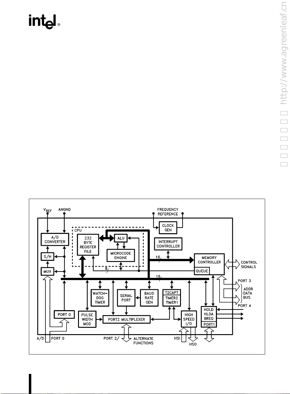
The 80C196KB can be separated into four sections for
the purpose of describing its operation. A block diagram is shown in Figure 1-1. There is the CPU and
architecture, the instruction set, the peripherals and the
bus unit. Each of the sections will be sub-divided as the
discussion progresses. Let us first examine the CPU.
1.0 CPU OPERATION
The major components of the CPU on the 80C196KB
are the Register File and the Register/Arithmetic Logic Unit (RALU). Communication with the outside
world is done through either the Special Function Registers (SFRs) or the Memory Controller. The RALU
does not use an accumulator. Instead, it operates directly on the 256-byte register space made up of the
Register File and the SFRs. Efficient I/O operations
are possible by directly controlling the I/O through the
SFRs. The main benefits of this structure are the ability
to quickly change context, absence of accumulator bottleneck, and fast throughput and I/O times.
270651– 1
Figure 1-1. 80C196KB Block Diagram
1
Page 6

80C196KB USER’S GUIDE
数控原理与维修 http://www.agreenleaf.cn
The CPU on the 80C196KB is 16 bits wide and connects to the interrupt controller and the memory controller by a 16-bit bus. In addition, there is an 8-bit bus
which transfers instruction bytes from the memory controller to the CPU. An extension of the 16-bit bus connects the CPU to the peripheral devices.
1.1 Memory Controller
The RALU talks to the memory, except for the locations in the register file and SFR space, through the
memory controller. Within the memory controller is a
bus controller, a four byte queue and a Slave Program
Counter (Slave PC). Both the internal ROM/EPROM
bus and the external memory bus are driven by the bus
controller. Memory access requests to the bus controller can come from either the RALU or the queue, with
queue accesses having priority. Requests from the
queue are always for instruction at the address in the
slave PC.
By having program fetches from memory referenced to
the slave PC, the processor saves time as addresses seldom have to be sent to the memory controller. If the
address sequence changes because of a jump, interrupt,
call or return, the slave PC is loaded with a new value,
the queue is flushed, and processing continues.
Execution speed is increased by using a queue since it
usually keeps the next instruction byte available. The
instruction execution times shown in Section 3 show
the normal execution times with no wait states added
and the 16-bit bus selected. Reloading the slave PC and
fetching the first byte of the new instruction stream
takes 4 state times. This is reflected in the jump taken/
not-taken times shown in the table.
REGISTER/ALU (RALU)
Most calculations performed by the 80C196KB take
place in the RALU. The RALU, shown in Figure 1-2,
contains a 17-bit ALU, the Program Status Word
(PSW), the Program Counter (PC), a loop counter, and
three temporary registers. All of the registers are 16bits or 17-bits (16
registers have the ability to perform simple operations
to off-load the ALU.
A separate incrementor is used for the Program Counter (PC) as it accesses operands. However, PC changes
due to jumps, calls, returns and interrupts must be handled through the ALU. Two of the temporary registers
have their own shift logic. These registers are used for
the operations which require logical shifts, including
Normalize, Multiply, and Divide. The ‘‘Lower Word’’
and ‘‘Upper Word’’ are used together for the 32-bit
instructions and as temporary registers for many instructions. Repetitive shifts are counted by the 6-bit
‘‘Loop Counter’’.
A third temporary register stores the second operand of
two operand instructions. This includes the multiplier
during multiplications and the divisor during divisions.
To perform subtractions, the output of this register can
be complemented before being placed into the ‘‘B’’ input of the ALU.
Several constants, such as 0, 1 and 2 are stored in the
RALU to speed up certain calculations. (e.g. making a
2’s complement number or performing an increment or
decrement instruction.) In addition, single bit masks for
bit test instructions are generated in the constant register based on the 3-bit Bit Select register.
a
sign extension) wide. Some of the
When debugging code using a logic analyzer, one must
be aware of the queue. It is not possible to determine
when an instruction will begin executing by simply
watching when it is fetched, since the queue is filled in
advance of instruction execution.
1.2 CPU Control
A microcode engine controls the CPU, allowing it to
perform operations with any byte, word or double word
in the 256 byte register space. Instructions to the CPU
are taken from the queue and stored temporarily in the
instruction register. The microcode engine decodes the
instructions and generates the correct sequence of
events to have the RALU perform the desired function.
Figure 1-2 shows the memory controller, RALU, instruction register and the control unit.
2
1.3 Internal Timing
The 80C196KB requires an input clock on XTAL1 to
function. Since XTAL1 and XTAL2 are the input and
output of an inverter a crystal can be used to generate
the clock. Details of the circuit and suggestions for its
use can be found in Section 13.
Internal operation of the 80C196KB is based on the
crystal or external oscillator frequency divided by 2.
Every 2 oscillator periods is referred to as one ‘‘state
time’’, the basic time measurement for all 80C196KB
operations. With a 12 MHz oscillator, a state time is
167 nanoseconds. With an 8 MHz oscillator, a state
time is 250 nanoseconds, the same as an 8096BH running with a 12 MHz oscillator. Since the 80C196KB
will be run at many frequencies, the times given
throughout this chapter will be in state times or
‘‘states’’, unless otherwise specified. A clock out
Page 7

80C196KB USER’S GUIDE
数控原理与维修 http://www.agreenleaf.cn
master PC
270651– 2
Figure 1-2. RALU and Memory Controller Block Diagram
3
Page 8
80C196KB USER’S GUIDE
数控原理与维修 http://www.agreenleaf.cn
约8K(8064字节)
48K
约8K(7934字节)
程序代码
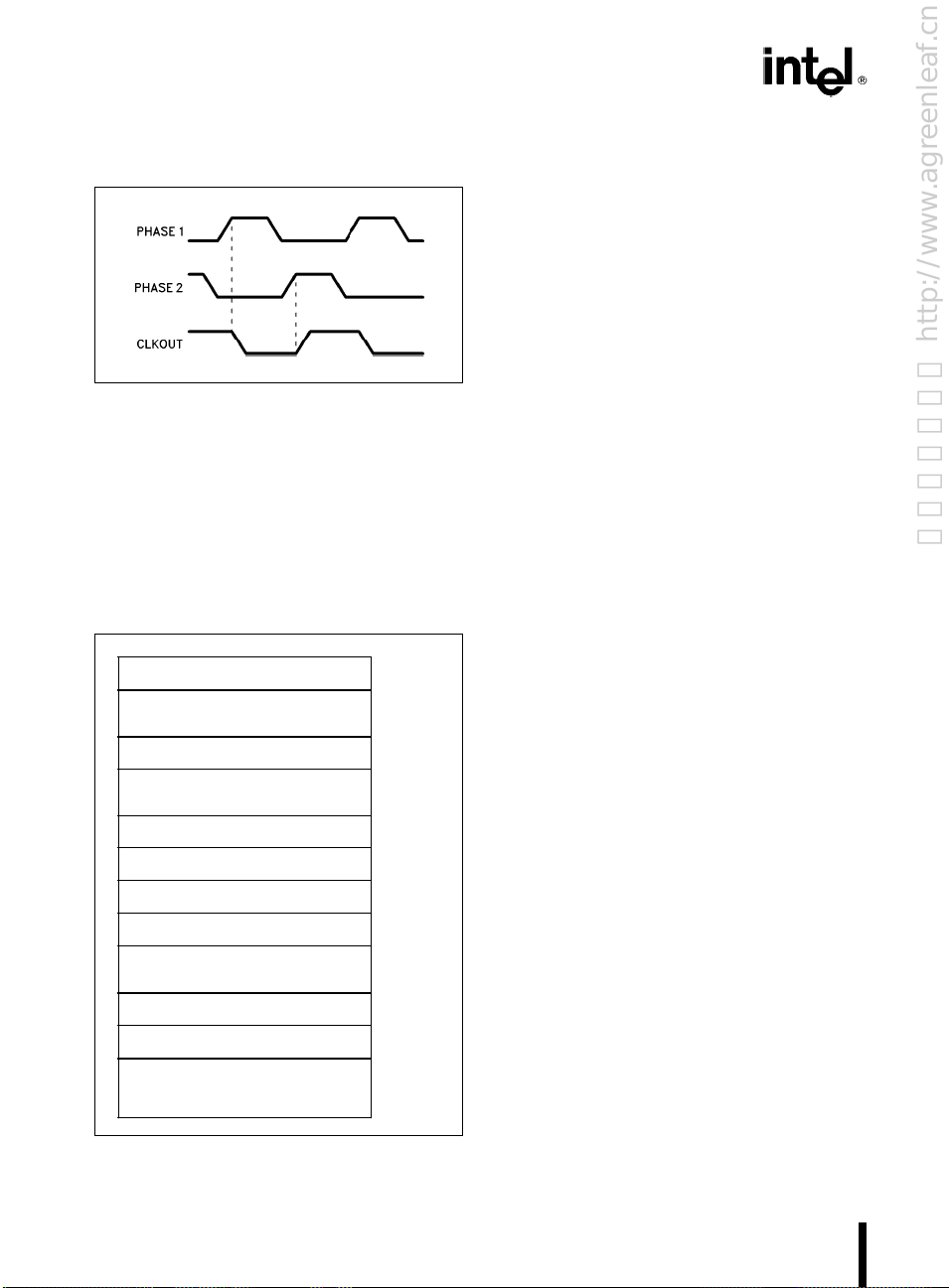
(CLKOUT) signal, shown in Figure 1-3, is provided as
an indication of the internal machine state. Details on
timing relationships can be found in Section 13.
270651– 3
Figure 1-3. Internal Clock Waveforms
2.0 MEMORY SPACE
The addressable memory space on the 80C196KB consists of 64K bytes, most of which is available to the user
for program or data memory. Locations which have
special purposes are 0000H through 00FFH and
1FFEH through 2080H. All other locations can be
used for either program or data storage or for memory
mapped peripherals. A memory map is shown in Figure
2-1.
EXTERNAL MEMORY OR I/O
INTERNAL ROM/EPROM OR
EXTERNAL MEMORY*
RESERVED
UPPER 8 INTERRUPT VECTORS
(NEW ON 80C196KB)
ROM/EPROM SECURITY KEY
RESERVED
CHIP CONFIGURATION BYTE
RESERVED
LOWER 8 INTERRUPT VECTORS
PLUS 2 SPECIAL INTERRUPTS
PORT 3 AND PORT 4
EXTERNAL MEMORY OR I/O
INTERNAL DATA MEMORY - REGISTER FILE
(STACK POINTER, RAM AND SFRS)
EXTERNAL PROGRAM CODE MEMORY
0FFFFH
4000H
2080H
2040H
2030H
2020H
2019H
2018H
2014H
2000H
1FFEH
0100H
0000H
2.1 Register File
Locations 00H through 0FFH contain the Register File
and Special Function Registers, (SFRs). The RALU
can operate on any of these 256 internal register locations, but code can not be executed from them. If an
attempt to execute instructions from locations 000H
through 0FFH is made, the instructions will be fetched
from external memory. This section of external memory is reserved for use by Intel development tools
The internal RAM from location 018H (24 decimal) to
0FFH is the Register File. It contains 232 bytes of
RAM which can be accessed as bytes (8 bits), words
(16 bits), or double-words (32 bits). Since each of these
locations can be used by the RALU, there are essentially 232 ‘‘accumulators’’. This memory region, as well as
the status of the majority of the chip, is kept intact
while the chip is in the Powerdown Mode. Details on
Powerdown Mode are discussed in Section 14.
Locations 18H and 19H contain the stack pointer.
These are not SFRs and may be used as standard RAM
if stack operations are not being performed. Since the
stack pointer is in this area, the RALU can easily operate on it. The stack pointer must be initialized by the
user program and can point anywhere in the 64K memory space. Operations to the stack cause it to build
down, so the stack pointer should be initialized to 2
bytes above the highest stack location, and must be
word aligned.
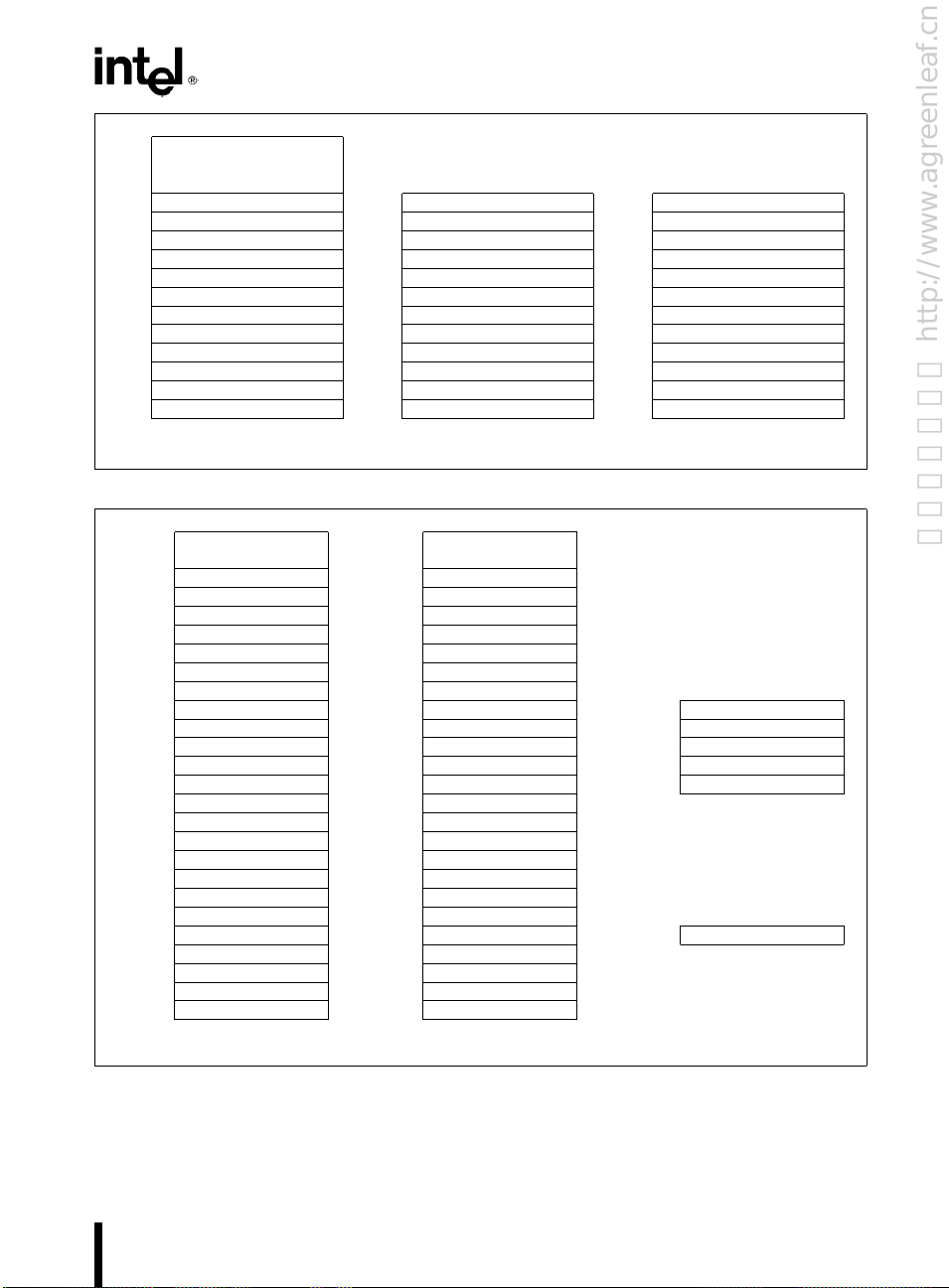
2.2 Special Function Registers
Locations 00H through 17H are the I/O control registers or SFRs. All of the peripheral devices on the
80C196KB (except Ports 3 and 4) are controlled
through these registers. As shown in Figure 2-2, three
SFR windows are provided on the 80C196KB.
Switching between the windows is done using the Window Select Register (WSR) at location 14H in all of the
windows. The PUSHA and POPA instructions push
and pop the WSR so it is easy to change between windows. Only three values may be written to the WSR, 0,
14 and 15. Other values are reserved for use in future
parts and will cause unpredictable operation.
Window 0, the register window selected with WSR
is a superset of the one used on the 8096BH. As depicted in Figure 2-3, it has 24 registers, some of which have
different functions when read than when written. Registers which are new to the 80C196KB or have changed
functions from the 8096 are indicated in the figure.
e
0,
Figure 2-1. 80C196KB Memory Map
4
Page 9
Listed registers
数控原理与维修 http://www.agreenleaf.cn
are present in
all three windows
16H 16H 16H
14H
12H
10H 10H 10H
0EH 0EH 0EH
0CH
0AH 0AH 0AH
08H
06H 06H 06H
04H 04H 04H
02H 02H 02H
00H
WSR
INT MASK1/PEND1
TIMER2
INT MASK/PEND
ZERO REG
READ/WRITE PROGRAMMING WRITE/READ
e
0 WSRe14 WSRe15
WSR
14H
12H
0CH
08H
00H
WSR
INT MASK1/PEND1
T2 CAPTURE
INT MASK/PEND
ZERO REG
14H
12H
0CH
08H
00H
Figure 2-2. Multiple Register Windows
80C196KB USER’S GUIDE
WSR
INT MASK1/PEND1
T2 CAPTURE
INT MASK/PEND
ZERO REG
19H
18H 18H
17H *IOS2 17H PWMÐCONTROL
16H IOS1 16H IOC1
15H IOS0 15H IOC0
14H *WSR 14H *WSR
13H *INTÐMASK 1 13H *INTÐMASK 1
12H *INTÐPEND 1 12H *INTÐPEND 1
11H *SPÐSTAT 11H *SPÐCON
10H PORT2 10H PORT2 10H RESERVED**
0FH PORT1 0FH PORT1 0FH RESERVED**
0EH PORT0 0EH BAUD RATE 0EH RESERVED**
0DH TIMER2 (HI) 0DH TIMER2 (HI) 0DH *T2 CAPTURE (HI)
0CH TIMER2 (LO) 0CH TIMER2 (LO) 0CH *T2 CAPTURE (LO)
0BH TIMER1 (HI) 0BH *IOC2
0AH TIMER1 (LO) 0AH WATCHDOG
09H INTÐPEND 09H INTÐPEND OTHER SFRS IN WSR 15 BECOME
08H INTÐMASK 08H INTÐMASK
07H SBUF(RX) 07H SBUF(TX)
06H HSIÐSTATUS 06H HSOÐCOMMAND
05H HSIÐTIME (HI) 05H HSOÐTIME (HI)
04H HSIÐTIME (LO) 04H HSOÐTIME (LO) 04H PPW
03H ADÐRESULT (HI) 03H HSIÐMODE WSRe14
02H ADÐRESULT (LO) 02H ADÐCOMMAND
01H ZERO REG (HI) 01H ZERO REG (HI) *NEW OR CHANGED REGISTER
00H ZERO REG (LO) 00H ZERO REG (LO)
STACK POINTER
WHEN READ WHEN WRITTEN
19H
e
0 BE WRITTEN OR READ
WSR
STACK POINTER
READABLE IF THEY WERE WRITABLE
IN WSR
WERE READABLE IN WSR
FUNCTION FROM 8096BH
**RESERVED REGISTERS SHOULD NOT
WSR
e
0, AND WRITABLE IF THEY
e
e
15
0
Figure 2-3. Special Function Registers
5
Page 10
80C196KB USER’S GUIDE
数控原理与维修 http://www.agreenleaf.cn
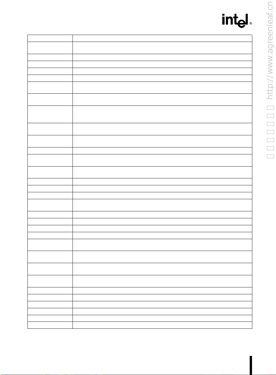
Register Description
R0 Zero Register - Always reads as a zero, useful for a base when indexing and as a
ADÐRESULT A/D Result Hi/Low - Low and high order results of the A/D converter
ADÐCOMMAND A/D Command Register - Controls the A/D
HSIÐMODE HSI Mode Register - Sets the mode of the High Speed Input unit.
HSIÐTIME HSI Time Hi/Lo - Contains the time at which the High Speed Input unit was triggered.
HSOÐTIME HSO Time Hi/Lo - Sets the time or count for the High Speed Output to execute the
HSOÐCOMMAND HSO Command Register - Determines what will happen at the time loaded into the
HSIÐSTATUS HSI Status Registers - Indicates which HSI pins were detected at the time in the HSI
SBUF(TX) Transmit buffer for the serial port, holds contents to be outputted. Last written value
SBUF(RX) Receive buffer for the serial port, holds the byte just received by the serial port.
INTÐMASK Interrupt Mask Register - Enables or disables the individual interrupts.
INTÐPEND Interrupt Pending Register - Indicates that an interrupt signal has occurred on one of
WATCHDOG Watchdog Timer Register - Written periodically to hold off automatic reset every 64K
TIMER1 Timer 1 Hi/Lo - Timer1 high and low bytes.
TIMER2 Timer 2 Hi/Lo - Timer2 high and low bytes.
IOPORT0 Port 0 Register - Levels on pins of Port 0. Reserved in Window 15.
BAUDÐRATE Register which determines the baud rate, this register is loaded sequentially.
IOPORT1 Port 1 Register - Used to read or write to Port 1. Reserved in Window 15
IOPORT2 Port 2 Register - Used to read or write to Port 2. Reserved in Window 15
SPÐSTAT Serial Port Status - Indicates the status of the serial port.
SPÐCON Serial Port Control - Used to set the mode of the serial port.
IOS0 I/O Status Register 0 - Contains information on the HSO status. Writes to HSO pins
IOS1 I/O Status Register 1 - Contains information on the status of the timers and of the
IOC0 I/O Control Register 0 - Controls alternate functions of HSI pins, Timer 2 reset
IOC1 I/O Control Register 1 - Controls alternate functions of Port 2 pins, timer interrupts
PWMÐCONTROL Pulse Width Modulation Control Register - Sets the duration of the PWM pulse.
INTÐPEND1 Interrupt Pending register for the 8 new interrupt vectors (also INTÐPENDING1)
INTÐMASK1 Interrupt Mask register for the 8 new interrupt vectors
IOC2 I/O Control Register 2 - Controls new 80C196KB features
IOS2 I/O Status Register 2 - Contains information on HSO events
WSR Window Select Register - Selects register window
constant for calculations and compares.
command in the Command Register.
HSO Time registers.
Time registers and the current state of the pins. In Window 15 - Writes to pin
detected bits, but not current state bits.
is readable in Window 15.
Writable in Window 15.
the sources and has not been serviced. (also INTÐPENDING)
state times. Returns upper byte of WDT counter in Window 15.
Reserved in Window 15.
in Window 15.
HSI.
sources and Timer 2 clock sources.
and HSI interrupts.
Figure 2-4. Special Function Register Description
6
Page 11

80C196KB USER’S GUIDE
数控原理与维修 http://www.agreenleaf.cn
Programming control and test operations are done in
Window 14. Registers in this window that are not labeled should be considered reserved and should not be
either read or written.
In register Window 15 (WSR
the SFRs is changed, so that those which were readonly in Window 0 space are write-only and vice versa.
The only major exception to this is that Timer2 is read/
write in Window 0, and T2 Capture is read/write
ADÐCOMMAND (02H) Ð Read the last written command
ADÐRESULT (02H, 03H) Ð Write a value into the result register
HSIÐMODE (03H) Ð Read the value in HSIÐMODE
HSIÐTIME (04H, 05H) Ð Write to FIFO Holding register
HSOÐTIME (04H, 05H) Ð Read the last value placed in the holding register
HSIÐSTATUS (06H) Ð Write to status bits but not to HSI pin bits. (Pin bits are 1, 3, 5, 7)
HSOÐCOMMAND (06H) Ð Read the last value placed in the holding register
SBUF(RX) (07H) Ð Write a value into the receive buffer
SBUF(TX) (07H) Ð Read the last value written to the transmit buffer
WATCHDOG (0AH) Ð Read the value in the upper byte of the WDT
TIMER1 (0AH, 0BH) Ð Write a value to Timer1
TIMER2 (0CH, 0DH) Ð Read/Write the Timer2 capture register.
IOC2 (0BH) Ð Last written value is readable, except bit 7 (Note 1)
BAUDÐRATE (0EH) Ð No function, cannot be read
PORT0 (0EH) Ð No function, no output drivers on the pins
SPÐSTAT (11H) Ð Set the status bits, TI and RI can be set, but it will not cause an interrupt
SPÐCON (11H) Ð Read the current control byte
IOS0 (15H) Ð Writing to this register controls the HSO pins. Bits 6 and 7 are inactive for
IOC0 (15H) Ð Last written value is readable, except bit 1 (Note 1)
IOS1 (16H) Ð Writing to this register will set the status bits, but not cause interrupts. Bits
IOC1 (16H) Ð Last written value is readable
IOS2 (17H) Ð Writing to this register will set the status bits, but not cause interrupts.
PWMÐCONTROL (17H) Ð Read the duty cycle value written to PWMÐCONTROL
NOTE:
1. IOC2.7 (CAM CLEAR) and IOC0.1 (T2RST) are not latched and will read as a 1 (precharged bus).
Being able to write to the read-only registers and vice-versa provides a lot of flexibility. One of the most useful
advantages is the ability to set the timers and HSO lines for initial conditions other than zero.
e
15), the operation of
(Timer2 read/write is done with WSR
writes.
6 and 7 are not functional.
in Window 15. (Timer2 was read-only on the 8096.)
Registers which can be read and written in Window 0
can also be read and written in Window 15.
Figure 2-4 contains brief descriptions of the SFR registers. Detailed descriptions are contained in the section
which discusses the peripheral controlled by the register. Figure 2-5 contains a description of the alternate
function in Window 15.
e
0)
Figure 2-5. Alternate SFR Function in Window 15
7
Page 12

80C196KB USER’S GUIDE
数控原理与维修 http://www.agreenleaf.cn
Within the SFR space are several registers and bit locations labeled ‘‘RESERVED’’. These locations should
never be written or read. A reserved bit location should
always be written with 0 to maintain compatibility with
future parts. Values read from these locations may
change from part to part or over temperature and voltage. Registers and bits which are not labeled should be
treated as reserved registers and bits. Note that the default state of internal registers is 0, while that for external memory is 1. This is because SFR functions are
typically disabled with a zero, while external memory is
typically erased to all 1s.
Caution must be taken when using the SFRs as sources
of operations or as base or index registers for indirect or
indexed operations. It is possible to get undesired results, since external events can change SFRs and some
SFRs clear when read. The potential for an SFR to
change value must be taken into account when operating on these registers. This is particularly important
when high level languages are used as they may not
always make allowances for SFR-type registers. SFRs
can be operated on as bytes or words unless otherwise
specified.
2.3 Reserved Memory Spaces
Locations 1FFEH and 1FFFH are used for Ports 3 and
4 respectively, allowing easy reconstruction of these
ports if external memory is used. An example of reconstructing the I/O ports is given in Section 15. If ports 3
and 4 are not going to be reconstructed and internal
ROM/EPROM is not used, these locations can be
treated as any other external memory location.
Many reserved and special locations are in the memory
area between 2000H and 2080H. In this area the 18
interrupt vectors, chip configuration byte, and security
key are located. Figure 2-6 shows the locations and
functions of these registers. The interrupts, chip configuration, and security key registers are discussed in Sections 5, 16, and 17 respectively. With one exception, all
unspecified addresses in locations 2000H through
207FH, including those marked ‘‘Reserved’’ are reserved by Intel for use in testing or future products.
They must be filled with the Hex value FFH to insure
compatibility with future devices. Location 2019H
should contain 20H to prevent possible bus contention
during the CCB fetch cycle. NOTE: 1. This exception
applies only to systems with a 16-bit bus and external
program memory. 2. Previously designed systems
which do not experience bus contention don’t need to
change the contents of this location. Refer to Section
15.2 for more information about bus contention during
CCB fetch.
EXTERNAL MEMORY
OR I/O
INTERNAL PROGRAM
STORAGE ROM/EPROM
OR
EXTERNAL MEMORY 2080H
RESERVED 2074H– 207FH
VOLTAGE LEVELS 2072H –2073H
SIGNATURE WORD 2070H– 2071H
RESERVED 2040H– 206FH
INTERRUPT VECTORS 2030H –203FH
SECURITY KEY 2020H– 202FH
RESERVED 2019H– 201FH
CHIP CONFIGURATION BYTE 2018H
RESERVED 2015H– 2017H
PPW 2014H
INTERRUPT VECTORS 2000H– 2013H
FFFFH
4000H
Figure 2-6. Reserved Memory Spaces
Resetting the 80C196KB causes instructions to be
fetched starting from location 2080H. This location was
chosen to allow a system to have up to 8K of RAM
continuous with the register file. Further information
on reset can be found in Section 13.
2.4 Internal ROM and EPROM
When a ROM part is ordered, or an EPROM part is
programmed, the internal memory locations 2080H
through 3FFFH are user specified, as are the interrupt
vectors, Chip Configuration Register and Security Key
in locations 2000H through 207FH. Location 2014H
contains the PPW (Programming Pulse Width) register. The PPW is used solely to program 87C196KB
EPROM devices and is a reserved location on ROM
and ROMless devices.
Instruction and data fetches from the internal ROM or
EPROM occur only if the part has ROM or EPROM,
EA
is tied high, and the address is between 2000H and
3FFFH. At all other times data is accessed from either
the internal RAM space or external memory and instructions are fetched from external memory. The EA
pin is latched on RESET rising. Information on programming EPROMs can be found in Section 16.
8
Page 13

80C196KB USER’S GUIDE
数控原理与维修 http://www.agreenleaf.cn
The 80C196KB provides a ROM/EPROM lock feature
to allow the program to be locked against reading
and/or writing the internal program memory. In order
to maintain security, code can not be executed out of
the last three locations of internal ROM/EPROM if
the lock is enabled. Details on this feature are in Section 17.
2.5 System Bus
There are several modes of system bus operation on the
80C196KB. The standard bus mode uses a 16-bit multiplexed address/data bus. Other bus modes include an
8-bit mode and a mode in which the bus size can dynamically be switched between 8-bits and 16-bits.
Hold/Hold Acknowledge (HOLD
signals are available to create a variety of memory systems. The READY line extends the width of the RD
(read) and WR (write) pulses to allow access of slow
memories. Multiple processor systems with shared
memory can be designed using HOLD
the 80C196KB off the bus. Details on the System Bus
are in Section 15.
/HLDA) and Ready
/HLDA to keep
3.0 SOFTWARE OVERVIEW
This section provides information on writing programs
to execute in the 80C196KB. Additional information
can be found in the following documents:
MCSÉ-96 MACRO ASSEMBLER USER’S GUIDE
Order Number 122048 (Intel Systems)
Order Number 122351 (DOS Systems)
MCS
-96 UTILITIES USER’S GUIDE
É
Order Number 122049 (Intel Systems)
Order Number 122356 (DOS Systems)
PL/M-96 USER’S GUIDE
Order Number 122134 (Intel Systems)
Order Number 122361 (DOS Systems)
C-96 USER’S GUIDE
Order Number 167632 (DOS Systems)
Throughout this chapter short sections of code are used
to illustrate the operation of the device. For these sections it is assumed that the following set of temporary
registers has been declared:
AX, BX, CX, and DX are 16-bit registers.
AL is the low byte of AX, AH is the high byte.
BL is the low byte of BX
CL is the low byte of CX
DL is the low byte of DX
These are the same as the names for the general data
registers used in the 8086. It is important to note that in
the 80C196KB these are not dedicated registers but
merely the symbolic names assigned by the programmer to an eight byte region within the on-board register
file.
3.1 Operand Types
The MCS-96 architecture supports a variety of data
types likely to be useful in a control application. To
avoid confusion, the name of an operand type is capitalized. A ‘‘BYTE’’ is an unsigned eight bit variable; a
‘‘byte’’ is an eight bit unit of data of any type.
BYTES
BYTES are unsigned 8-bit variables which can take on
the values between 0 and 255. Arithmetic and relational
operators can be applied to BYTE operands but the
result must be interpreted in modulo 256 arithmetic.
Logical operations on BYTES are applied bitwise. Bits
within BYTES are labeled from 0 to 7, with 0 being the
least significant bit.
WORDS
WORDS are unsigned 16-bit variables which can take
on the values between 0 and 65535. Arithmetic and
relational operators can be applied to WORD operands
but the result must be interpreted modulo 65536. Logical operations on WORDS are applied bitwise. Bits
within words are labeled from 0 to 15 with 0 being the
least significant bit. WORDS must be aligned at even
byte boundaries in the MCS-96 address space. The least
significant byte of the WORD is in the even byte address and the most significant byte is in the next higher
(odd) address. The address of a word is the address of
its least significant byte. Word operations to odd addresses are not guaranteed to operate in a consistent
manner.
SHORT-INTEGERS
SHORT-INTEGERS are 8-bit signed variables which
can take on the values between
Arithmetic operations which generate results outside of
the range of a SHORT-INTEGER will set the overflow
indicators in the program status word. The actual numeric result returned will be the same as the equivalent
operation on BYTE variables.
b
128 anda127.
9
Page 14

80C196KB USER’S GUIDE
数控原理与维修 http://www.agreenleaf.cn
INTEGERS
INTEGERS are 16-bit signed variables which can take
on the values between
metic operations which generate results outside of the
range of an INTEGER will set the overflow indicators
in the program status word. The actual numeric result
returned will be the same as the equivalent operation on
WORD variables. INTEGERS conform to the same
alignment and addressing rules as do WORDS.
BITS
BITS are single-bit operands which can take on the
Boolean values of true and false. In addition to the normal support for bits as components of BYTE and
WORD operands, the 80C196KB provides for the direct testing of any bit in the internal register file. The
MCS-96 architecture requires that bits be addressed as
components of BYTES or WORDS, it does not support
the direct addressing of bits that can occur in the MCS51 architecture.
DOUBLE-WORDS
DOUBLE-WORDS are unsigned 32-bit variables
which can take on the values between 0 and
4,294,967,295. The MCS-96 architecture provides direct support for this operand type for shifts, as the dividend in a 32-by-16 divide and the product of a 16-by-16
multiply, and for double-word comparisons. For these
operations a DOUBLE-WORD variable must reside in
the on-board register file of the 80C196KB and be
aligned at an address which is evenly divisible by 4. A
DOUBLE-WORD operand is addressed by the address
of its least significant byte. DOUBLE-WORD operations which are not directly supported can be easily
implemented with two WORD operations. For consistency with Intel provided software the user should adopt
the conventions for addressing DOUBLE-WORD operands which are discussed in Section 3.5.
LONG-INTEGERS
LONG-INTEGERS are 32-bit signed variables which
can take on the values between
a
2,147,483,647. The MCS-96 architecture provides direct support for this data type for shifts, as the dividend
in a 32-by-16 divide and the product of a 16-by-16 multiply, and for double-word comparisons.
b
32,768 anda32,767. Arith-
b
2,147,483,648 and
LONG-INTEGERS can also be normalized. For these
operations a LONG-INTEGER variable must reside in
the onboard register file of the 80C196KB and be
aligned at an address which is evenly divisible by 4. A
LONG-INTEGER is addressed by the address of its
least significant byte.
LONG-INTEGER operations which are not directly
supported can be easily implemented with two INTEGER operations. For consistency with Intel provided
software, the user should adopt the conventions for addressing LONG operands which are discussed in Section 3.6.
3.2 Operand Addressing
Operands are accessed within the address space of the
80C196KB with one of six basic addressing modes.
Some of the details of how these addressing modes
work are hidden by the assembly language. If the programmer is to take full advantage of the architecture, it
is important that these details be understood. This section will describe the addressing modes as they are handled by the hardware. At the end of this section the
addressing modes will be described as they are seen
through the assembly language. The six basic address
modes which will be described are termed register-direct, indirect, indirect with auto-increment, immediate,
short-indexed, and long-indexed. Several other useful
addressing operations can be achieved by combining
these basic addressing modes with specific registers
such as the ZERO register or the stack pointer.
REGISTER-DIRECT REFERENCES
The register-direct mode is used to directly access a
register from the 256 byte on-board register file. The
register is selected by an 8-bit field within the instruction and the register address must conform to the operand type’s alignment rules. Depending on the instruction, up to three registers can take part in the calculation.
Examples
ADD AX,BX,CX ; AX:4BX0CX
MUL AX,BX ; AX:4AX*BX
INCB CL ; CL:4CL01
10
Page 15

INDIRECT REFERENCES
数控原理与维修 http://www.agreenleaf.cn
in advance
The indirect mode is used to access an operand by placing its address in a WORD variable in the register file.
The calculated address must conform to the alignment
rules for the operand type. Note that the indirect address can refer to an operand anywhere within the address space of the 80C196KB, including the register
80C196KB USER’S GUIDE
file. The register which contains the indirect address is
selected by an eight bit field within the instruction. An
instruction can contain only one indirect reference and
the remaining operands of the instruction (if any) must
be register-direct references.
Examples
LD AX,[AX] ; AX:4MEM
ADDB AL,BL,[CX] ; AL:4BL0MEM
POP [AX] ; MEM
INDIRECT WITH AUTO-INCREMENT REFERENCES
This addressing mode is the same as the indirect mode
except that the WORD variable which contains the indirect address is incremented after it is used to address
the operand. If the instruction operates on BYTES or
Examples
LD AX,[BX]0 ; AX:4MEM
ADDB AL,BL,[CX]0 ; AL:4BL0MEM
PUSH [AX]0 ; SP:4SP12;
IMMEDIATE REFERENCES
This addressing mode allows an operand to be taken
directly from a field in the instruction. For operations
on BYTE or SHORT-INTEGER operands this field is
eight bits wide. For operations on WORD or
Examples
ADD AX,#340 ; AX:4AX0340
PUSH #1234H ; SP:4SP12; MEM
DIVB AX,#10 ; AL:4AX/10; AH:4AX MOD 10
WORD(AX):4MEM WORD(SP); SP:4SP02
; MEM
; AX:4AX02
WORD(AX)
BYTE(CX)
SHORT-INTEGERS the indirect address variable will
be incremented by one. If the instruction operates on
WORDS or INTEGERS the indirect address variable
will be incremented by two.
WORD(BX); BX:4BX02
BYTE(CX); CX:4CX01
WORD(SP):4MEM WORD(AX)
INTEGER operands the field is 16 bits wide. An instruction can contain only one immediate reference and
the remaining operand(s) must be register-direct references.
WORD(SP):41234H
SHORT-INDEXED REFERENCES
In this addressing mode an eight bit field in the instruction selects a WORD variable in the register file which
contains an address. A second eight bit field in the instruction stream is sign-extended and summed with the
WORD variable to form the address of the operand
which will take part in the calculation.
Examples
LD AX,12[BX] ; AX:4MEM
MULB AX,BL,3[CX] ; AX:4BL*MEM
Since the eight bit field is sign-extended, the effective
address can be up to 128 bytes before the address in the
WORD variable and up to 127 bytes after it. An instruction can contain only one short-indexed reference
and the remaining operand(s) must be register-direct
references.
WORD(BX012)
BYTE(CX03)
11
Page 16
80C196KB USER’S GUIDE
数控原理与维修 http://www.agreenleaf.cn
LONG-INDEXED REFERENCES
This addressing mode is like the short-indexed mode
except that a 16-bit field is taken from the instruction
and added to the WORD variable to form the address
of the operand. No sign extension is necessary. An in-
struction can contain only one long-indexed reference
and the remaining operand(s) must be register-direct
references.
Examples
AND AX,BX,TABLE[CX] ; AX:4BX AND MEM
ST AX,TABLE[BX] ; MEM
ADDB AL,BL,LOOKUP[CX] ; AL:4BL0MEM
ZERO REGISTER ADDRESSING
The first two bytes in the register file are fixed at zero
by the 80C196KB hardware. In addition to providing a
fixed source of the constant zero for calculations and
comparisons, this register can be used as the WORD
Examples
ADD AX,1234[0] ; AX:4AX0MEM
POP 5678[0] ; MEM
STACK POINTER REGISTER ADDRESSING
The system stack pointer in the 80C196KB is accessed
as register 18H of the internal register file. In addition
to providing for convenient manipulation of the stack
pointer, this also facilitates the accessing of operands in
the stack. The top of the stack, for example, can be
Examples
PUSH [SP] ; DUPLICATE TOP
LD AX,2[SP] ; AX:4NEXT
WORD(5678):4MEM WORD(SP)
; SP:4SP02
WORD(TABLE0BX):4AX
WORD(TABLE0CX)
BYTE(LOOKUP0CX)
variable in a long-indexed reference. This combination
of register selection and address mode allows any location in memory to be addressed directly.
WORD(1234)
accessed by using the stack pointer as the WORD variable in an indirect reference. In a similar fashion, the
stack pointer can be used in the short-indexed mode to
access data within the stack.
OF STACK
TO TOP
ASSEMBLY LANGUAGE ADDRESSING MODES
The MCS-96 assembly language simplifies the choice of
addressing modes to be used in several respects:
Direct Addressing. The assembly language will choose
between register-direct addressing and long-indexed
with the ZERO register depending on where the operand is in memory. The user can simply refer to an operand by its symbolic name: if the operand is in the register file, a register-direct reference will be used, if the
operand is elsewhere in memory, a long-indexed reference will be generated.
Indexed Addressing. The assembly language will
choose between short and long indexing depending on
the value of the index expression. If the value can be
expressed in eight bits then short indexing will be used,
if it cannot be expressed in eight bits then long indexing
will be used.
12
These features of the assembly language simplify the
programming task and should be used wherever possible.
3.3 Program Status Word
The program status word (PSW) is a collection of Boolean flags which retain information concerning the state
of the user’s program. There are two bytes in the PSW;
the actual status word and the low byte of the interrupt
mask. Figure 3-1 shows the status bits of the PSW. The
PSW can be saved in the system stack with a single
operation (PUSHF) and restored in a like manner
(POPF). Only the interrupt section of the PSW can be
accessed directly. There is no SFR for the PSW status
bits.
Page 17

80C196KB USER’S GUIDE
数控原理与维修 http://www.agreenleaf.cn
CONDITION FLAGS
The PSW bits on the 80C196KB are set as follows:
PSW:
76543210
ZNVVTCX IST
Figure 3-1. PSW Register
Z: The Z (Zero) flag is set to indicate that the opera-
tion generated a result equal to zero. For the addwith-carry (ADDC) and subtract-with-borrow
(SUBC) operations the Z flag is cleared if the result is non-zero but is never set. These two instructions are normally used in conjunction with
the ADD and SUB instructions to perform multiple precision arithmetic. The operation of the Z
flag for these instructions leaves it indicating the
proper result for the entire multiple precision calculation.
N: The Negative flag is set to indicate that the opera-
tion generated a negative result. Note that the N
flag will be in the algebraically correct state even
if an overflow occurs. For shift operations, including the normalize operation and all three forms
(SHL, SHR, SHRA) of byte, word and double
word shifts, the N flag will be set to the same
value as the most significant bit of the result. This
will be true even if the shift count is 0.
V: The oVerflow flag is set to indicate that the opera-
tion generated a result which is outside the range
for the destination data type. For the SHL, SHLB
and SHLL instructions, the V flag will be set if the
most significant bit of the operand changes at any
time during the shift. For divide operations, the
following conditions are used to determine if the V
flag is set:
For the
operation: V is set if Quotient is:
UNSIGNED
BYTE DIVIDE
UNSIGNED
WORD DIVIDE
SIGNED
BYTE or
DIVIDE
SIGNED
WORD or
DIVIDE
l
255(0FFH)
l
65535(0FFFFH)
k
b
127(81H)
l
127(7FH)
k
b
32767(8001H)
l
32767(7FFFH)
VT: The oVerflow Trap flag is set when the V flag is
set, but it is only cleared by the CLRVT, JVT and
JNVT instructions. The operation of the VT flag
allows for the testing for a possible overflow condition at the end of a sequence of related arithmetic operations. This is normally more efficient
than testing the V flag after each instruction.
C: The Carry flag is set to indicate the state of the
arithmetic carry from the most significant bit of
the ALU for an arithmetic operation, or the state
of the last bit shifted out of an operand for a shift.
Arithmetic Borrow after a subtract operation is
the complement of the C flag (i.e. if the operation
generated a borrow then C
e
0.)
X: Reserved. Should always be cleared when writing
to the PSW for compatibility with future products.
I: The global Interrupt disable bit disables all inter-
rupts when cleared except NMI, TRAP, and unimplemented opcode.
ST: The ST (STicky bit) flag is set to indicate that
during a right shift a 1 has been shifted first into
the C flag and then been shifted out. The ST flag
is undefined after a multiply operation. The ST
flag can be used along with the C flag to control
rounding after a right shift. Consider multiplying
two eight bit quantities and then scaling the result
down to 12 bits:
MULUB AX,CL,DL ;AX:4CL*DL
SHR AX,#4 ;Shift right 4
places
If the C flag is set after the shift, it indicates that the
bits shifted off the end of the operand were greater-than
or equal-to one half the least significant bit (LSB) of the
result. If the C flag is clear after the shift, it indicates
that the bits shifted off the end of the operand were less
than half the LSB of the result. Without the ST flag,
the rounding decision must be made on the basis of the
C flag alone. (Normally the result would be rounded up
if the C flag is set.) The ST flag allows a finer resolution
in the rounding decision:
C ST Value of the Bits Shifted Off
0 0 Valuee0
010
k
Valuek(/2 LSB
1 0 Valuee(/2 LSB
1 1 Valuel(/2 LSB
Figure 3-2. Rounding Alternatives
Imprecise rounding can be a major source of error in a
numerical calculation; use of the ST flag improves the
options available to the programmer.
13
Page 18

80C196KB USER’S GUIDE
数控原理与维修 http://www.agreenleaf.cn
INTERRUPT FLAGS
The lower eight bits of the PSW individually mask the
lowest 8 sources of interrupt to the 80C196KB. These
mask bits can be accessed as an eight bit byte (INT
MASKÐaddress 8) in the on-board register file. A separate register (INTÐMASK1Ðaddress 13H) contains
the control bits for the higher 8 interrupts. A logical ‘1’
in these bit positions enables the servicing of the corresponding interrupt. Bit 9 in the PSW is the global interrupt disable. If this bit is cleared then interrupts will be
locked out. Note that the interrupts are collected in the
INTÐPEND registers even if they are locked out. Execution of the corresponding service routines will proceed according to their priority when they become enabled. Further information on the interrupt structure of
the 80C196KB can be found in Section 5.
3.4 Instruction Set
The MCS-96 instruction set contains a full set of arithmetic and logical operations for the 8-bit data types
BYTE and SHORT INTEGER and for the 16-bit data
types WORD and INTEGER. The DOUBLE-WORD
and LONG data types (32 bits) are supported for the
products of 16-by-16 multiplies and the dividends of
32-by-16 divides, for shift operations, and for 32-bit
compares. The remaining operations on 32-bit variables
can be implemented by combinations of 16-bit operations. As an example the sequence:
ADD AX,CX
ADDC BX,DX
performs a 32-bit addition, and the sequence
SUB AX,CX
SUBC BX,DX
performs a 32-bit subtraction. Operations on REAL
(i.e. floating point) variables are not supported directly
by the hardware but are supported by the floating point
library for the 80C196KB (FPAL-96) which implements a single precision subset of draft 10 of the IEEE
standard for floating point arithmetic. The performance
of this software is significantly improved by the
80C196KB NORML instruction which normalizes a
32-bit variable and by the existence of the ST flag in the
PSW.
In addition to the operations on the various data types,
the 80C196KB supports conversions between these
types. LDBZE (load byte zero extended) converts a
BYTE to a WORD and LDBSE (load byte sign extended) converts a SHORT-INTEGER into an INTEGER.
WORDS can be converted to DOUBLE-WORDS by
simply clearing the upper WORD of the DOUBLEWORD (CLR) and INTEGERS can be converted to
LONGS with the EXT (sign extend) instruction.
Ð
The MCS-96 instructions for addition, subtraction, and
comparison do not distinguish between unsigned words
and signed integers. Conditional jumps are provided to
allow the user to treat the results of these operations as
either signed or unsigned quantities. As an example, the
CMPB (compare byte) instruction is used to compare
both signed and unsigned eight bit quantities. A JH
(jump if higher) could be used following the compare if
unsigned operands were involved or a JGT (jump if
greater-than) if signed operands were involved.
Tables 3-1 and 3-2 summarize the operation of each of
the instructions. Complete descriptions of each instruction and its timings can be found in the MCS-96 family
Instruction Set chapter.
The execution times for the instruction set are given in
Figure 3-3. These times are given for a 16-bit bus with
no wait states. On-chip EPROM/ROM space is a 16bit, zero wait state bus. When executing from an 8-bit
external memory system or adding wait states, the CPU
becomes bus limited and must sometimes wait for the
prefetch queue. The performance penalty for an 8-bit
external bus is difficult to measure, but has shown to be
between 10 and 30 percent based on the instruction
mix. The best way to measure code performance is to
actually benchmark the code and time it using an emulator or with TIMER1.
The indirect and indexed instruction timings are given
for two memory spaces: SFR/Internal RAM space (0–
0FFH), and a memory controller reference (100H–
0FFFFH). Any instruction that uses an operand that is
referenced through the memory controller (ex. Add
r1,5000H[0]) takes 2– 3 states longer than if the operand was in the SFR/Internal RAM space. Any data
access to on-chip ROM/EPROM is considered to be a
memory controller reference.
Flag Settings. The modification to the flag setting is
shown for each instruction. A checkmark (
that the flag is set or cleared as appropriate. A hyphen
means that the flag is not modified. A one or zero (1) or
(0) indicates that the flag will be in that state after the
instruction. An up arrow (
struction may set the flag if it is appropriate but will
not clear the flag. A down arrow (
flag can be cleared but not set by the instruction. A
question mark (?) indicates that the flag will be left in
an indeterminant state after the operation.
) indicates that the in-
u
) indicates that the
v
&
) means
14
Page 19

80C196KB USER’S GUIDE
数控原理与维修 http://www.agreenleaf.cn
Table 3-1A. Instruction Summary
Mnemonic Operands Operation (Note 1)
ADD/ADDB 2 DwDaA
ADD/ADDB 3 DwBaA
ADDC/ADDCB 2 DwDaAaC
SUB/SUBB 2 DwDbA
SUB/SUBB 3 DwBbA
SUBC/SUBCB 2 DwDbAaCb1
CMP/CMPB 2 DbA
MUL/MULU 2 D,Da2
MUL/MULU 3 D,Da2
MULB/MULUB 2 D,Da1
MULB/MULUB 3 D,Da1
DIVU 2 Dw(D,Da2) /A,Da2wremainder
DIVUB 2 Dw(D,Da1) /A,Da1wremainder
DIV 2 Dw(D,Da2) /A,Da2wremainder
DIVB 2 Dw(D,Da1) /A,Da1wremainder
AND/ANDB 2 DwD AND A
AND/ANDB 3 DwB AND A
OR/ORB 2 DwDORA
XOR/XORB 2 DwD (ecxl. or) A
LD/LDB 2 DwA
ST/STB 2 AwD
LDBSE 2 DwA; Da1wSIGN(A)
LDBZE 2 DwA; Da1w0
PUSH 1 SPwSPb2; (SP)wA
POP 1 Aw(SP); SPa2
PUSHF 0 SPwSPb2; (SP)wPSW; 0 0 0 0 0 0
POPF 0 PSWw(SP); SPwSPa2; I
SJMP 1 PCwPCa11-bit offset
LJMP 1 PCwPCa16-bit offset
BR[indirect
SCALL 1 SPwSPb2;
LCALL 1 SPwSPb2; (SP)wPC;
]
PSW
1PC
(SP)
PCwPCa16-bit offset
w
DcA
w
BcA
w
DcA
w
BcA
w
0000H; Iw0
w
(A)
w
PC; PC
w
PCa11-bit offset
w
Z N C V VT ST
&&&&
&&&&
v
&&&&
&&&&
v
&&&&
bbbbb b
bbbbb b
bbbbb b
bbbbb b
bbb
bbb
bbb
bbb
&&
&&
&&
&&
bbbbb b
bbbbb b
bbbbb b
bbbbb b
bbbbb b
bbbbb b
& &&&& & &
bbbbb b
bbbbb b
bbbbb b
bbbbb b
bbbbb b
Flags
&&&
&&&
&
&
&
&
00
00
00
00
u
u
u
u
u
u
u
u
u
u
u
bb
bb
bb
bb
b
b
b
b
b
b
b
b
b
b
b
Notes
2
2
3
3
2
3
3,4
3,4
5
5
5
5
15
Page 20
80C196KB USER’S GUIDE
数控原理与维修 http://www.agreenleaf.cn
Table 3-1B. Instruction Summary
Mnemonic Operands Operation (Note 1)
RET 0 PCw(SP); SP
J (conditional) 1 PCwPCa8-bit offset (if taken)
JC 1 Jump if Ce1
JNC 1 jump if Ce0
JE 1 jump if Ze1
JNE 1 Jump if Ze0
JGE 1 Jump if Ne0
JLT 1 Jump if Ne1
JGT 1 Jump if Ne0 and Ze0
JLE 1 Jump if Ne1orZe1
JH 1 Jump if Ce1 and Ze0
JNH 1 Jump if Ce0orZe1
JV 1 Jump if Ve1
JNV 1 Jump if Ve0
JVT 1 Jump if VTe1; Clear VT
JNVT 1 Jump if VTe0; Clear VT
JST 1 Jump if STe1
JNST 1 Jump if STe0
JBS 3 Jump if Specified Bite1
JBC 3 Jump if Specified Bite0
DJNZ/ 1 D
DJNZW If D
DEC/DECB 1 D
NEG/NEGB 1 D
INC/INCB 1 D
EXT 1 D
EXTB 1 D
NOT/NOTB 1 D
CLR/CLRB 1 D
SHL/SHLB/SHLL 2 Cwmsb-----lsbw0
SHR/SHRB/SHRL 2 0xmsb-----lsbxC
SHRA/SHRAB/SHRAL 2 msbxmsb-----lsbxC
SETC 0 Cw1
CLRC 0 Cw0
b bbbb b b
w
Db1;
i
0 then PCwPCa8-bit offset 10
w
Db1
w
0bD
w
Da1
w
D; Da2wSign (D)
w
D; Da1wSign (D)
w
Logical Not (D)
w
0 1000
w
SPa2
Flags
Z N C V VT ST
bbbb b b
bbbb b b
bbbb b b
bbbb b b
bbbb b b
bbbb b b
bbbb b b
bbbb b b
bbbb b b
bbbb b b
bbbb b b
bbbb b b
bbbb b b
bbbb0b
bbbb0b
bbbb b b
bbbb b b
bbbb b b
bbbb b b
bbbb b b
0
0
b
u
b
u
b
u
bb
bb
bb
bb
b
u
b
&
b
&
&&&&
&&&&
&&&&
&&
00
&&
00
&&
00
&&&&
&&&
&&&
bb1bb b
bb0bb b
Notes
5
5
5
5
5
5
5
5
5
5
5
5
5
5
5
5
5
5,6
5,6
5
2
3
7
7
7
16
Page 21
Table 3-1C. Instruction Summary
数控原理与维修 http://www.agreenleaf.cn
Mnemonic Operands Operation (Note 1)
CLRVT 0 VTw0
RST 0 PC
DI 0 Disable All Interupts (Iw0)
EI 0 Enable All Interupts (Iw1)
NOP 0 PC
SKIP 0 PC
NORML 2 Left shift till msbe1; Dwshift count
TRAP 0 SPwSPb2;
PUSHA 1 SPwSP-2; (SP)
POPA 1 IMASK1/WSRw(SP); SPwSPa2
IDLPD 1 IDLE MODE IF KEYe1;
CMPL 2 D-A
BMOV 2
w
2080H 0 0 0 0 0 0 8
w
PCa1
w
PCa2
(SP)wPC; PCw(2010H)
w
PSW
w
0000H; SP
w
(SP)
PSWw(SP); SPwSPa2
POWERDOWN MODE IF KEYe2;
CHIP RESET OTHERWISE
[
PTRÐHI
UNTIL COUNTe0
IMASK1/WSR; IMASK1w00H
a
]
w
PSW; 0 0 0 0 0 0
w
SP-2;
[
PTRÐLOW
a
]
;
80C196KB USER’S GUIDE
Flags
Z N C V VT ST
bbbb
bbbb b b
bbbb b b
bbbb b b
bbbb b b
&&
bbbb b b
&&&& & &
bbbb b b
&&&&
bbbb b b
bb b
0
0
u
b
b
Notes
7
9
NOTES:
1. If the mnemonic ends in ‘‘B’’ a byte operation is performed, otherwise a word operation is done. Operands D, B, and A
must conform to the alignment rules for the required operand type. D and B are locations in the Register File; A can be
located anywhere in memory.
a
2. D,D
3. D,D
4. Changes a byte to word.
5. Offset is a 2’s complement number.
6. Specified bit is one of the 2048 bits in the register file.
7. The ‘‘L’’ (Long) suffix indicates double-word operation.
8. Initiates a Reset by pulling RESET
2080H.
9. The assembler will not accept this mnemonic.
10. The DJNZW instruction is not guaranteed to work. See Functional Deviations section.
2 are consecutive WORDS in memory; D is DOUBLE-WORD aligned.
a
1 are consecutive BYTES in memory; D is WORD aligned.
low. Software should re-initialize all the necessary registers with code starting at
17
Page 22

80C196KB USER’S GUIDE
数控原理与维修 http://www.agreenleaf.cn
Table 3-2A. Instruction Length (in Bytes)/Opcode
MNEMONIC DIRECT IMMED
NORMAL*
ADD (3-op) 4/44 5/45 4/46 4/46 5/47 6/47
SUB (3-op) 4/48 5/49 4/4A 4/4A 5/4B 6/4B
ADD (2-op) 3/64 4/65 3/66 3/66 4/67 5/67
SUB (2-op) 3/68 4/69 3/6A 3/6A 4/6B 5/6B
ADDC 3/A4 4/A5 3/A6 3/A6 4/A7 5/A7
SUBC 3/A8 4/A9 3/AA 3/AA 4/AB 5/AB
CMP 3/88 4/89 3/AB 3/AB 4/8B 5/8B
ADDB (3-op) 4/54 4/55 4/56 4/56 5/57 6/57
SUBB (3-op) 4/58 4/59 4/5A 4/5A 5/5B 6/5B
ADDB (2-op) 3/74 3/75 3/76 3/76 4/77 5/77
SUBB (2-op) 3/78 3/79 3/7A 3/7A 4/7B 5/7B
ADDCB 3/B4 3/B5 3/B6 3/B6 4/B7 5/B7
SUBCB 3/B8 3/B9 3/BA 3/BA 4/BB 5/BB
CMPB 3/98 3/99 3/9A 3/9A 4/9B 5/9B
MUL (3-op) 5/
(2)
6/
(2)
MULU (3-op) 4/4C 5/4D 4/4E 4/4E 5/4F 6/4F
MUL (2-op) 4/
(2)
5/
(2)
MULU (2-op) 3/6C 4/6D 3/6E 3/6E 4/6F 5/6F
DIV 4/
(2)
5/
(2)
DIVU 3/8C 4/8D 3/8E 3/8E 4/8F 5/8F
MULB (3-op) 5/
(2)
5/
(2)
MULUB (3-op) 4/5C 4/5D 4/5E 4/5E 5/5F 6/5F
MULB (2-op) 4/
(2)
4/
(2)
MULUB (2-op) 3/7C 3/7D 3/7E 3/7E 4/7F 5/7F
DIVB 4/
(2)
4/
(2)
DIVUB 3/9C 3/9D 3/9E 3/9E 4/9F 5/9F
AND (3-op) 4/40 5/41 4/42 4/42 5/43 6/43
AND (2-op) 3/60 4/61 3/62 3/62 4/63 5/63
OR (2-op) 3/80 4/81 3/82 3/82 4/83 5/83
XOR 3/84 4/85 3/86 3/86 4/87 5/87
ANDB (3-op) 4/50 4/51 4/52 4/52 5/53 5/53
ANDB (2-op) 3/70 3/71 3/72 3/72 4/73 4/73
ORB (2-op) 3/90 3/91 3/92 3/92 4/93 5/93
XORB 3/94 3/95 3/96 3/96 4/97 5/97
PUSH 2/C8 3/C9 2/CA 2/CA 3/CB 4/CB
POP 2/CC Ð 2/CE 2/CE 3/CF 4/CF
INDIRECT INDEXED
5/
4/
4/
5/
4/
4/
(1)
(2)
(2)
(2)
(2)
(2)
(2)
A-INC*
(2)
5/
(2)
4/
(2)
4/
(2)
5/
(2)
4/
(2)
4/
(1)
SHORT*
(2)
6/
(2)
5/
(2)
5/
(2)
6/
(2)
5/
(2)
5/
(1)
LONG*
7/
6/
6/
7/
6/
6/
(1)
(2)
(2)
(2)
(2)
(2)
(2)
NOTES:
1. Indirect and indirect
indirect or short indexed. If odd, use indirect or long indexed.
2. The opcodes for signed multiply and divide are the unsigned opcode with an ‘‘FE’’ prefix.
a
share the same opcodes, as do short and long indexed opcodes. If the second byte is even, use
18
Page 23
80C196KB USER’S GUIDE
数控原理与维修 http://www.agreenleaf.cn
Table 3-2B. Instruction Length (in Bytes)/Opcode
MNEMONIC DIRECT IMMED
LD 3/A0 4/A1 3/A2 3/A2 4/A3 5/A3
LDB 3/B0 3/B1 3/B2 3/B2 4/B3 5/B3
ST 3/C0 Ð 3/C2 3/C2 4/C3 5/C3
STB 3/C4 Ð 3/C6 3/C6 4/C7 5/C7
LDBSE 3/BC 3/BD 3/BE 3/BE 4/BF 5/BF
LBSZE 3/AC 3/AD 3/AE 3/AE 4/AF 5/AF
INDIRECT INDEXED
NORMAL A-INC SHORT LONG
Mnemonic Length/Opcode
PUSHF 1/F2
POPF 1/F3
PUSHA 1/F4
POPA 1/F5
TRAP 1/F7
LCALL 3/EF
SCALL 2/28– 2F
RET 1/F0
LJMP 3/E7
SJMP 2/20 –27
[]
BR
JNST 1/D0
JST 1/D8
JNH 1/D1
JH 1/D9
JGT 1/D2
JLE 1/DA
JNC 1/B3
JC 1/D8
JNVT 1/D4
JVT 1/DC
JNV 1/D5
JV 1/DD
JGE 1/D6
JLT 1/DE
JNE 1/D7
JE 1/DF
JBC 3/30 –37
JBS 3/38–3F
NOTES:
3. The 3 least significant bits of the opcode are concatenated with the 8 bits to form an 11-bit, 2’s complement offset.
4. The DJNZW instruction is not guaranteed to work. See Functional Deviations section.
2/E3
(3)
(3)
Mnemonic Length/Opcode
DJNZ 3/E0
DJNZW 3/E1
NORML 3/0F
SHRL 3/0C
SHLL 3/0D
SHRAL 3/0E
SHR 3/08
SHRB 3/18
SHL 3/09
SHLB 3/19
SHRA 3/0A
SHRAB 3/1A
CLRC 1/F8
SETC 1/F9
DI 1/FA
EI 1/FB
CLRVT 1/FC
NOP 1/FD
RST 1/FF
SKIP 2/00
IDLPD 1/F6
BMOV 3/C1
(4)
19
Page 24

80C196KB USER’S GUIDE
数控原理与维修 http://www.agreenleaf.cn
Table 3.3A. Instruction Execution State Times
MNEMONIC DIRECT IMMED
INDIRECT INDEXED
(1)
NORMAL* A-INC* SHORT* LONG*
ADD (3-op) 5 6 7/10 8/11 7/10 8/11
SUB (3-op) 5 6 7/10 8/11 7/10 8/11
ADD (2-op) 4 5 6/8 7/9 6/8 7/9
SUB (2-op) 4 5 6/8 7/9 6/8 7/9
ADDC 4 5 6/8 7/9 6/8 7/9
SUBC 4 5 6/8 7/9 6/8 7/9
CMP 4 5 6/8 7/9 6/8 7/9
ADDB (3-op) 5 5 7/10 8/11 7/10 8/11
SUBB (3-op) 5 5 7/10 8/11 7/10 8/11
ADDB (2-op) 4 4 6/8 7/9 6/8 7/9
SUBB (2-op) 4 4 6/8 7/9 6/8 7/9
ADDCB 4 4 6/8 7/9 6/8 7/9
SUBCB 4 4 6/8 7/9 6/8 7/9
CMPB 4 4 6/8 7/9 6/8 7/9
MUL (3-op) 16 17 18/21 19/22 19/22 20/23
MULU (3-op) 14 15 16/19 17/19 17/20 18/21
MUL (2-op) 16 17 18/21 19/22 19/22 20/23
MULU (2-op) 14 15 16/19 17/19 17/20 18/21
DIV 26 27 28/31 29/32 29/32 30/33
DIVU 24 25 26/29 27/30 27/30 28/31
MULB (3-op) 12 12 14/17 13/15 15/18 16/19
MULUB (3-op) 10 10 12/15 12/16 12/16 14/17
MULB (2-op) 12 12 14/17 15/18 15/18 16/19
MULUB (2-op) 10 10 12/15 13/15 12/16 14/17
DIVB 18 18 20/23 21/24 21/24 22/25
DIVUB 16 16 18/21 19/22 19/22 20/23
AND (3-op) 5 6 7/10 8/11 7/10 8/11
AND (2-op) 4 5 6/8 7/9 6/8 7/9
OR (2-op) 4 5 6/8 7/9 6/8 7/9
XOR 4 5 6/8 7/9 6/8 7/9
ANDB (3-op) 5 5 7/10 8/11 7/10 8/11
ANDB (2-op) 4 4 6/8 7/9 6/8 7/9
ORB (2-op) 4 4 6/8 7/9 6/8 7/9
XORB 4 4 6/8 7/9 6/8 7/9
LD, LDB 4, 4 5, 4 5/8 6/8 6/9 7/10
ST, STB 4, 4
b
5/8 6/9 6/9 7/10
LDBSE 4 4 5/8 6/8 6/9 7/10
LDBZE 4 4 5/8 6/8 6/9 7/10
BMOV internal/internal: 6a8 per word
external/internal: 6
external/external: 6
a
11 per word
a
14 per word
PUSH (int stack) 6 7 9/12 10/13 10/13 11/14
POP (int stack) 8
b
10/12 11/13 11/13 12/14
PUSH (ext stack) 8 9 11/14 12/15 12/15 13/16
POP (ext stack) 11
*Times for operands as: SFRs and internal RAM (0 –1FFH)/memory controller (200H –0FFFFH)
NOTE:
1. Execution times for memory controller references may be one to two states higher depending on the number of bytes in
the prefetch queue. Internal stack is 200H– 1FFH and external stack is 200H –0FFFFH.
b
13/15 14/16 14/16 15/17
20
Page 25

80C196KB USER’S GUIDE
数控原理与维修 http://www.agreenleaf.cn
Table 3.3B. Instruction Execution State Times
MNEMONIC MNEMONIC
PUSHF (int stack) 6 PUSHF (ext stack) 8
POPF (int stack) 7 POPF (ext stack) 10
PUSHA (int stack) 12 PUSHA (ext stack) 18
POPA (int stack) 12 POPA (ext stack) 18
TRAP (int stack) 16 TRAP (ext stack) 18
LCALL (int stack) 11 LCALL (ext stack) 13
SCALL (int stack) 11 SCALL (ext stack) 13
RET (int stack) 11 RET (ext stack) 14
CMPL 7 DEC/DECB 3
CLR/CLRB 3 EXT/EXTB 4
NOT/NOTB 3 INC/INCB 3
NEG/NEGB 3
LJMP 7
SJMP 7
BR[indirect
JNST, JST 4/8 jump not taken/jump taken
JNH, JH 4/8 jump not taken/jump taken
JGT, JLE 4/8 jump not taken/jump taken
JNC, JC 4/8 jump not taken/jump taken
JNVT, JVT 4/8 jump not taken/jump taken
JNV, JV 4/8 jump not taken/jump taken
JGE, JLT 4/8 jump not taken/jump taken
JNE, JE 4/8 jump not taken/jump taken
JBC, JBS 5/9 jump not taken/jump taken
DJNZ 5/9 jump not taken/jump taken
DJNZW (Note 1) 5/9 jump not taken/jump taken
NORML 8a1 per shift (9 for 0 shift)
SHRL 7
SHLL 7
SHRAL 7
SHR/SHRB 6
SHL/SHLB 6
SHRA/SHRAB 6a1 per shift (7 for 0 shift)
CLRC 2
SETC 2
DI 2
EI 2
CLRVT 2
NOP 2
RST 15 (includes fetch of configuration byte)
SKIP 3
IDLPD 8/25 (proper key/improper key)
]
7
a
1 per shift (8 for 0 shift)
a
1 per shift (8 for 0 shift)
a
1 per shift (8 for 0 shift)
a
1 per shift (7 for 0 shift)
a
1 per shift (7 for 0 shift)
NOTE:
1. The DJNZW instruction is not guaranteed to work. See Functional Deviations section.
21
Page 26

80C196KB USER’S GUIDE
数控原理与维修 http://www.agreenleaf.cn
3.5 80C196KB Instruction Set Additions and Differences
For users already familiar with the 8096BH, there are
six instructions added to the standard MCS-96 instruction set to form the 80C196KB instruction set. All of
the former instructions perform the same function, except as indicated in the next section. The new instructions and their descriptions are listed below:
PUSHA Ð PUSHes the PSW, INTÐMASK, IM-
POPA Ð POPs the PSW, INTÐMASK, IMASK1,
IDLPD Ð Sets the part into IDLE or Powerdown
CMPL Ð Compare 2 long direct values
BMOV Ð Block move using 2 auto-incrementing
DJNZW Ð Decrement Jump Not Zero using a Word
INSTRUCTION DIFFERENCES
Instruction times on the 80C196KB are shorter than
those on the 8096 for many instructions. For example a
c
16
14 states. In addition, many zero and one operand instructions and most instructions using external data
take one or two fewer state times.
Indexed and indirect operations relative to the stack
pointer (SP) work differently on the 80C196KB than
on the 8096BH. On the 8096BH, the address is calculated based on the un-updated version of the stack
pointer. The 80C196KB uses the updated version. The
offset for POP[SP]and POP nn[SP]instructions may
need to be changed by a count of 2.
ASK1, and WSR
and WSR
mode
pointers and a counter
counter (Not functional on current stepping.)
16 unsigned multiply has been reduced from 25 to
3.6 Software Standards and Conventions
For a software project of any size it is a good idea to
modularize the program and to establish standards
which control the communication between these modules. The nature of these standards will vary with the
needs of the final application. A common component of
all of these standards, however, must be the mechanism
for passing parameters to procedures and returning results from procedures. In the absence of some overriding consideration which prevents their use, it is suggested that the user conform to the conventions adopted by
the PLM-96 programming language for procedure linkage. It is a very usable standard for both the assembly
language and PLM-96 environment and it offers compatibility between these environments. Another advantage is that it allows the user access to the same floating
point arithmetics library that PLM-96 uses to operate
on REAL variables.
REGISTER UTILIZATION
The MCS-96 architecture provides a 256 byte register
file. Some of these registers are used to control registermapped I/O devices and for other special functions
such as the ZERO register and the stack pointer. The
remaining bytes in the register file, some 230 of them,
are available for allocation by the programmer. If these
registers are to be used effectively, some overall strategy
for their allocation must be adopted. PLM-96 adopts
the simple and effective strategy of allocating the eight
bytes between addresses 1CH and 23H as temporary
storage. The starting address of this region is called
PLMREG. The remaining area in the register file is
treated as a segment of memory which is allocated as
required.
ADDRESSING 32-BIT OPERANDS
These operands are formed from two adjacent 16-bit
words in memory. The least significant word of the
double word is always in lower address, even when the
data is in the stack (which means that the most significant word must be pushed into the stack first). A double word is addressed by the address of its least significant byte. Note that the hardware supports some operations on double words. For these operations the double
word must be in the internal register file and must have
an address which is evenly divisible by four.
SUBROUTINE LINKAGE
Parameters are passed to subroutines in the stack. Parameters are pushed into the stack in the order that
they are encountered in the scanning of the source text.
Eight-bit parameters (BYTES or SHORT-INTEGERS) are pushed into the stack with the high order
byte undefined. Thirty-two bit parameters (LONG-INTEGERS, DOUBLE-WORDS, and REALS) are
pushed onto the stack as two 16-bit values; the most
significant half of the parameter is pushed into the
stack first.
As an example, consider the following PLM-96 procedure:
exampleÐprocedure: PROCEDURE
(param1,param2,param3);
DECLARE param1 BYTE,
param2 DWORD,
param3 WORD;
22
Page 27

80C196KB USER’S GUIDE
数控原理与维修 http://www.agreenleaf.cn
When this procedure is entered at run time the stack
will contain the parameters in the following order:
?????? : param1
high word of param2
low word of param2
param3
return address
Figure 3-5. Stack Image
If a procedure returns a value to the calling code (as
opposed to modifying more global variables) then the
result is returned in the variable PLMREG. PLMREG
is viewed as either an 8-, 16- or 32-bit variable depending on the type of the procedure.
The standard calling convention adopted by PLM-96
has several key features:
a) Procedures can always assume that the eight bytes of
register file memory starting at PLMREG can be
used as temporaries within the body of the procedure.
b) Code which calls a procedure must assume that the
eight bytes of register file memory starting at
PLMREG are modified by the procedure.
c) The Program Status Word (PSWÐsee Section 3.3) is
not saved and restored by procedures so the calling
code must assume that the condition flags (Z, N, V,
VT, C, and ST) are modified by the procedure.
d) Function results from procedures are always re-
turned in the variable PLMREG.
PLM-96 allows the definition of INTERRUPT procedures which are executed when a predefined interrupt
occurs. These procedures do not conform to the rules of
a normal procedure. Parameters cannot be passed to
these procedures and they cannot return results. Since
they can execute essentially at any time (hence the term
interrupt), these procedures must save the PSW and
PLMREG when they are entered and restore these values before they exit.
w
StackÐpointer
3.7 Software Protection Hints
Several features to assist in recovery from hardware
and software errors are available on the 80C196KB.
Protection is also provided against executing unimplemented opcodes by the unimplemented opcode interrupt. In addition, the hardware reset instruction (RST)
can cause a reset if the program counter goes out of
bounds. This instruction has an opcode of 0FFH, so if
the processor reads in bus lines which have been pulled
high it will reset itself.
It is recommended that unused areas of code be filled
with NOPs and periodic jumps to an error routine or
RST (reset chip) instructions. This is particularly important in the code around lookup tables, since if lookup tables are executed undesired results will occur.
Wherever space allows, each table should be surrounded by 7 NOPs (the longest 80C196KB instruction has 7
bytes) and a RST or jump to error routine instruction.
Since RST is a one-byte instruction, the NOPs are not
needed if RSTs are used instead of jumps to an error
routine. This will help to ensure a speedy recovery
should the processor have a glitch in the program flow.
The Watchdog Timer (WDT) further protects against
software and hardware errors. When using the WDT to
protect software it is desirable to reset it from only one
place in code, lessening the chance of an undesired
WDT reset. The section of code that resets the WDT
should monitor the other code sections for proper operation. This can be done by checking variables to make
sure they are within reasonable values. Simply using a
software timer to reset the WDT every 10 milliseconds
will provide protection only for catastrophic failures.
4.0 PERIPHERAL OVERVIEW
There are five major peripherals on the 80C196KB: the
pulse-width-modulated output (PWM), Timer1 and
Timer2, High Speed I/O Unit, Serial Port and A/D
Converter. With the exception of the high speed I/O
unit (HSIO), each of the peripherals is a single unit that
can be discussed without further separation.
Four individual sections make up the HSIO and work
together to form a very flexible timer/counter based
I/O system. Included in the HSIO are a 16-bit timer
(Timer1), a 16-bit up/down counter (Timer2), a programmable high speed input unit (HSI), and a programmable high speed output unit (HSO). With very
little CPU overhead the HSIO can measure pulse
widths, generate waveforms, and create periodic interrupts. Depending on the application, it can perform the
work of up to 18 timer/counters and capture/compare
registers.
A brief description of the peripheral functions and interractions is included in this section. It provides overview information prior to the detailed discussions in the
following sections. All of the details on control bits and
precautions are in the individual sections for each peripheral starting with Section 5.
23
Page 28

80C196KB USER’S GUIDE
数控原理与维修 http://www.agreenleaf.cn
4.1 Pulse Width Modulation Output (D/A)
Digital to analog conversion can be done with the Pulse
Width Modulation output. The output waveform is a
variable duty cycle pulse which repeats every 256 state
times or 512 state times if the prescaler is enabled.
Changes in the duty cycle are made by writing to the
PWM register. There are several types of motors which
require a PWM waveform for most efficient operation.
Additionally, if this waveform is integrated it will produce a DC level which can be changed in 256 steps by
varying the duty cycle. Details on the PWM are in Section 6.
4.2 Timers
Two 16-bit timers are available for use on the
80C196KB. The first is designated ‘‘Timer1’’, the second ‘‘Timer2’’. Timer1 is used to synchronize events to
real time, while Timer2 is clocked externally and synchronizes events to external occurrences. The timers
are the time bases for the High Speed Input (HSI) and
High Speed Output (HSO) units and can be considered
an integral part of the HSI/O. Details on the timers are
in Section 7.
Timer1 is a free-running timer which is incremented
every eight state times, just as it is on the 8096BH.
Timer1 can cause an interrupt when it overflows.
Timer2 counts transitions, both positive and negative,
on its input which can be either the T2CLK pin or the
HSI.1 pin. Timer2 can be read and written and can be
reset by hardware, software or the HSO unit. It can be
used as an up/down counter based on Port 2.6 and it’s
value can be captured into the T2CAPture register. Interrupts can be generated on capture events and if Timer2 crosses the 0FFFFH/0000H boundary or the
7FFFH/8000H boundary in either direction.
4.3 High Speed Inputs (HSI)
The High Speed Input (HSI) unit can capture the value
of Timer1 when an event takes place on one of four
input pins (HSI.0-HSI.3). Four types of events can trigger a capture: rising edges only, falling edges only, rising or falling edges, or every eighth rising edge. A block
diagram of this unit is shown in Figure 4-3. Details on
the HSI unit are in Section 8.
When events occur, the Timer1 value gets stored in the
FIFO along with 4 status bits which indicate the input
line(s) that caused the event. The next event ready to be
unloaded from the FIFO is placed in the HSI Holding
Register, so a total of 8 pieces of data can be stored in
the FIFO. Data is taken off the FIFO by reading the
HSIÐSTATUS register, followed by reading the
HSIÐTIME register. When the time register is read
the next FIFO location is loaded into the holding register.
Three forms of HSI interrupts can be generated: when a
value moves from the FIFO into the holding register;
when the FIFO (independent of the holding register)
has 4 or more events stored; and when the FIFO has 6
or more events stored. This flexibility allows optimization of the HSI for the expected frequency of interrupts.
Independent of the HSI operation, the state of the HSI
pins is indicated by 4 bits of the HSIÐSTATUS register. Also independent of the HSI operation is the HSI.0
pin interrupt, which can be used as an extra external
interrupt even if the pin is not enabled to the HSI unit.
4.4 High Speed Outputs (HSO)
The High Speed Output (HSO) unit can generate events
at specified times or counts based on Timer1 or Timer2
with minimal CPU overhead. A block diagram of the
HSO unit is shown in Figure 4-4. Up to 8 pending
events can be stored in the CAM (Content Addressable
Memory) of the HSO unit at one time. Commands are
placed into the HSO unit by first writing to HSO
COMMAND with the event to occur, and then to
HSOÐTIME with the timer match value.
Fourteen different types of events can be triggered by
the HSO: 8 external and 6 internal. There are two interrupt vectors associated with the HSO, one for external
events, and one for internal events. External events consist of switching one or more of the 6 HSO pins
(HSO.0-HSO.5). Internal events include setting up 4
Software Timers, resetting Timer2, and starting an A/
D conversion. The software timers are flags that can be
set by the HSO and optionally cause interrupts. Details
on the HSO Unit are in Section 9.
Ð
4.5 Serial Port
The serial port on the 80C196KB is functionally compatible with the serial port on the MCS-51 and MCS-96
families of microcontrollers. One synchronous and
three asynchronous modes are available. The asynchronous modes are full duplex, meaning they can transmit
and receive at the same time. Double buffering is provided for the receiver so that a second byte can be received before the first byte has been read. The transmitter is also double buffered, allowing bytes to be written
while transmission is still in progress.
The Serial Port STATus (SPÐSTAT) register contains
bits to indicate receive overrun, parity, and framing errors, and transmit and receive interrupts. Details on the
Serial Port are in Section 10.
24
Page 29
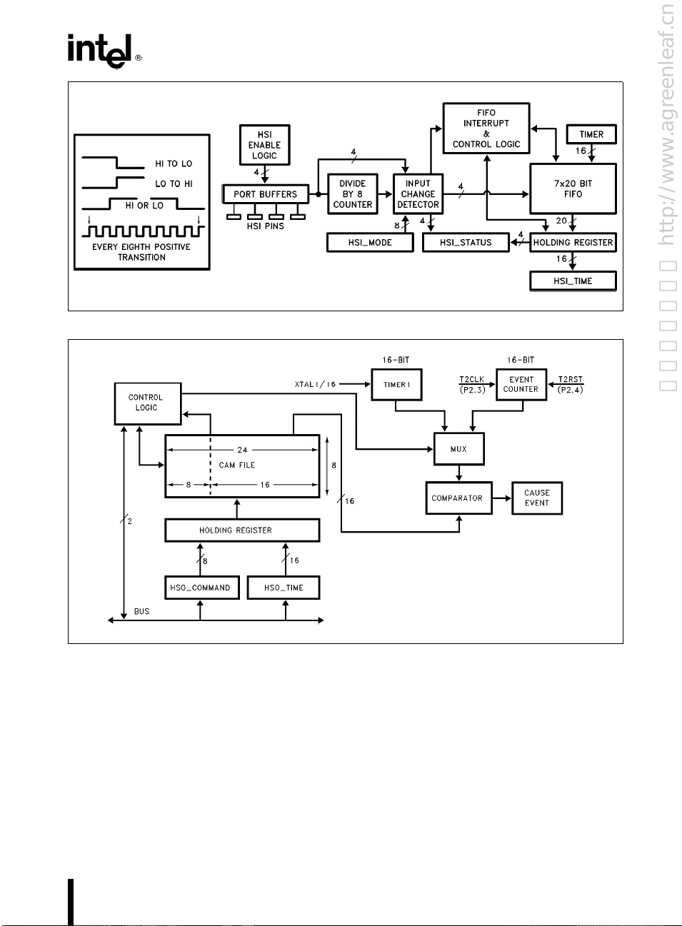
HSI Trigger Options
数控原理与维修 http://www.agreenleaf.cn
270651– 18
80C196KB USER’S GUIDE
270651– 19
Figure 4-3. HSI Block Diagram
HIGH SPEED OUTPUT CONTROLS
6 PINS
4 SOFTWARE TIMERS
2 INTERRUPTS
INITIATE A/D CONVERSION
RESET TIMER2
Figure 4-4. HSO Block Diagram
270651– 8
25
Page 30

80C196KB USER’S GUIDE
数控原理与维修 http://www.agreenleaf.cn
MODES OF OPERATION
Mode 0 is a synchronous mode which is commonly
used for shift register based I/O expansion. Sets of 8
bits are shifted in or out of the 80C196KB with a data
signal and a clock signal.
Mode 1 is the standard asynchronous communications
mode: the data frame used in this mode consists of 10
bits: a start bit (0), 8 data bits (LSB first), and a stop bit
(1). Parity can be enabled to send an even parity bit
instead of the 8th data bit and to check parity on reception.
Modes 2 and 3 are 9-bit modes commonly used for
multi-processor communications. The data frame used
in these modes consist of a start bit (0), 9 data bits (LSB
first), and a stop bit (1). When transmitting, the 9th
data bit can be set to a one to indicate an address or
other global transmission. Devices in Mode 2 will be
interrupted only if this bit is set. Devices in Mode 3 will
be interrupted upon any reception. This provides an
easy way to have selective reception on a data link.
Mode 3 can also be used to send and receive 8 bits of
data plus even parity.
BAUD RATES
Baud rates are generated in an independent 15-bit
counter based on either the T2CLK pin or XTAL1 pin.
Common baud rates can be easily generated with standard crystal frequencies. A maximum baud rate of 750
Kbaud is available in the asynchronous modes with
12MHz on XTAL1. The synchronous mode has a maximum rate of 3.0 Mbaud with a 12 MHz clock.
input at a time using successive approximation with a
result equal to the ratio of the input voltage divided by
the analog supply voltage. If the ratio is 1.00, then the
result will be all ones. A conversion can be started by
writing to the A/DÐCommand register or by an HSO
Command. Details on the A/D converter are in Section
11.
4.7 I/O Ports
There are five 8-bit I/O ports on the 80C196KB. Some
of these ports are input only, some are output only,
some are bidirectional and some have multiple functions. In addition to these ports, the HSI/O pins can be
used as standard I/O pins if their timer related features
are not needed.
Port 0 is an input port which is also the analog input
for the A/D converter. Port 1 is a quasi-bidirectional
port and the 3MSBs of Port 1 are multiplexed with the
HOLD
/HLDA functions. Port 2 contains three types
of port lines: quasi-bidirectional, input and output. Its
input and output lines are shared with other functions
such as serial port receive and transmit and Timer2
clock and reset. Ports 3 and 4 are open-drain bidirectional ports which share their pins with the address/
data bus.
Quasi-bidirectional pins can be used as input and output pins without the need for a data direction register.
They output a strong low value and a weak high value.
The weak high value can be externally pulled low providing an input function. A detailed explanation of
these ports can be found in Section 12.
4.6 A/D Converter
The 80C196KB’s Analog interface consists of a sampleand-hold, an 8-channel multiplexer, and a 10-bit successive approximation analog-to-digital converter.
Analog signals can be sampled by any of the 8 analog
input pins (ACH0 through ACH7) which are shared
with Port 0. An A/D conversion is performed on one
26
4.8 Watchdog Timer
The Watchdog Timer (WDT) provides a means to recover gracefully from a software upset. When the
watchdog is enabled it will initiate a hardware reset
unless the software clears it every 64K state times.
Hardware resets on the 80C196KB cause the RESET
input pin to be pulled low, providing a reset signal to
other components on the board. The WDT is independent of the other timers on the 80C196KB.
Page 31

80C196KB USER’S GUIDE
数控原理与维修 http://www.agreenleaf.cn
5.0 INTERRUPTS
Twenty-eight (28) sources of interrupts are available on
the 80C196KB. These sources are gathered into 15 vectors plus special vectors for NMI, the TRAP instruction, and Unimplemented Opcodes. Figure 5-1 shows
the routing of the interrupt sources into their vectors as
well as the control bits which enable some of the
sources.
Special Interrupts
Three special interrupts are available on the
80C196KB: NMI, TRAP and Unimplemented opcode.
The external NMI pin generates an unmaskable interrupt for implementation of critical interrupt routines.
The TRAP instruction is useful in the development of
custom software debuggers or generation of software
interrupts. The unimplemented opcode interrupt generates an interrupt when unimplemented opcodes are exe-
Figure 5-1. 80C196KB Interrupt Sources
270651– 9
27
Page 32

80C196KB USER’S GUIDE
数控原理与维修 http://www.agreenleaf.cn
cuted. This provides software recovery from random
execution during hardware and software failures. Although available for customer use, these interrupts may
be used in Intel development tools or evaluation boards.
NMI
NMI, the external Non-Maskable Interrupt, is the
highest priority interrupt. It vectors indirectly through
location 203EH. For design symmetry, a mask bit exists in INTÐMASK1 for the NMI. To prevent accidental masking of an NMI, the bit does not function
and will not stop an NMI from occurring. For future
compatibility, the NMI mask bit must be set to zero.
NMI on the 8096 vectored directly to location 0000H,
so for the 80C196KB to be compatible with 8096 software, which uses the NMI, location 203EH must be
loaded with 0000H. The NMI interrupt vector and interrupt vector location is used by some Intel development tools. For example, the EV80C196KB evaluation
board uses the NMI to process serial communication
interrupts from the host. The NMI interrupt routine
executes monitor commands passed from the host.
The NMI interrupt is sampled during PH1 or
CLKOUT low and is latched internally. If the pin is
held high, multiple interrupts will not occur.
TRAP
Opcode 0F7H, the TRAP instruction, causes an indirect vector through location 2010H. The TRAP instruction provides a single instruction interrupt useful
in designing software debuggers. The TRAP instruction prevents the acknowledgement of interrupts until
after execution of the next instruction.
Unimplemented Opcode
Opcodes which are not implemented on the 80C196KB
will cause an indirect vector through location 2012H.
User code or hardware which may have failed and run
into an unimplemented opcode can software recover
through this interrupt. The DJNZW instruction is not
supported on the 80C196KB but remains a valid opcode, therefore, no interrupt will occur.
The programmer must initialize the interrupt vector table with the starting addresses of the appropriate interrupt service routines. It is suggested that any unused
interrupts be vectored to an error handling routine. In a
debug environment, it may be desirable to have the routine lock into a jump to self loop which would be easily
traceable with emulation tools. More sophisticated routines may be appropriate for production code recoveries.
270651– 10
Figure 5-2. 80C196KB Interrupt Structure
Block Diagram
Five registers control the operation of the interrupt system: INTÐPEND, INTÐPEND1, INTÐMASK and
INTÐMASK1 and the PSW which contains a global
disable bit. A block diagram of the system is shown in
Figure 5-2. The transition detector looks for 0 to 1 transitions on any of the sources. External sources have a
maximum transition speed of one edge every state time.
Sampling will be guaranteed if the level on the interrupt
line is held for at least one state time. If the interrupt
line is not held for at least one state time, the interrupt
may not be detected.
28
Page 33

80C196KB USER’S GUIDE
数控原理与维修 http://www.agreenleaf.cn
5.1 Interrupt Control
Interrupt Pending Register
When the hardware detects one of the sixteen interrupts it sets the corresponding bit in one of two pending
interrupt registers (INTÐPEND-09H and INT
PEND1-12H). When the interrupt vector is taken, the
pending bit is cleared. These registers, the formats of
which are shown in Figure 5-3, can be read or modified
as byte registers. They can be read to determine which
of the interrupts are pending at any given time or modified to either clear pending interrupts or generate interrupts under software control. Any software which
modifies the INTÐPEND registers should ensure that
the entire operation is inseparable. The easiest way to
do this is to use the logical instructions in the two or
three operand format, for example:
ANDB INT
ORB INT
Caution must be used when writing to the pending register to clear interrupts. If the interrupt has already
been acknowledged when the bit is cleared, a 5 state
time ‘‘partial’’ interrupt cycle will occur. This is because the 80C196KB will have to fetch the next instruction of the normal instruction flow, instead of proceeding with the interrupt processing. The effect on the program will be essentially that of an extra two NOPs.
This can be prevented by clearing the bits using a 2
operand immediate logical, as the 80C196KB holds off
acknowledging interrupts during these ‘‘read/modify/
write’’ instructions.
Interrupt Mask Register
Individual interrupts can be enabled or disabled by setting or clearing bits in the interrupt mask registers
(INTÐMASK-08H and INTÐMASK1-13H). The
PEND,#11111101B
; Clears the A/D Interrupt
PEND,#00000010B
; Sets the A/D Interrupt
Ð
format of these registers is the same as that of the Interrupt Pending Register shown in Figure 5-3.
The INTÐMASK and INTÐMASK1 registers can be
read or written as byte registers. A one in any bit position will enable the corresponding interrupt source and
a zero will disable the source. The hardware will save
any interrupts that occur by setting bits in the pending
register, even if the interrupt mask bit is cleared. The
INTÐMASK register is the lower eight bits of the
PSW so the PUSHF and POPF instructions save and
restore the INTÐMASK register as well as the global
interrupt lockout and the arithmetic flags. Both the
INTÐMASK and INTÐMASK1 registers can be
saved with the PUSHA and POPA Instructions.
Global Disable
The processing of all interrupts except the NMI, TRAP
and unimplemented opcode interrupts can be disabled
by clearing the I bit in the PSW. Setting the I bit will
enable interrupts that have mask register bits which are
set. The I bit is controlled by the EI (Enable Interrupts)
and DI (Disable Interrupts) instructions. Note that the
I bit only controls the actual servicing of interrupts.
Interrupts that occur during periods of lockout will be
held in the pending register and serviced on a prioritized basis when the lockout period ends.
5.2 Interrupt Priorities
The priority encoder looks at all of the interrupts which
are both pending and enabled, and selects the one with
the highest priority. The priorities are shown in Figure
5-4 (15 is highest, 0 is lowest). The interrupt generator
then forces a call to the location in the indicated vector
location. This location would be the starting location of
the Interrupt Service Routine (ISR).
76543210
12H IPEND1:
13H IMASK1: FULL INT1 OVF CAP
09H IPEND: EXT SER SOFT HSI.0 HSO HSI A/D TIMER
08H IMASK: INT PORT TIMER PIN PIN DATA DONE OVF
NMI
76543210
Figure 5-3. Interrupt Mask and Pending Registers
FIFO EXT T2 T2
HSI4 RI TI
29
Page 34

80C196KB USER’S GUIDE
数控原理与维修 http://www.agreenleaf.cn
Number Source
INT15 NMI 203EH 15
INT14 HSI FIFO Full 203CH 14
INT13 EXTINT1 203AH 13
INT12 TIMER2 Overflow 2038H 12
INT11 TIMER2 Capture 2036H 11
INT10 4th Entry into HSI FIFO 2034H 10
INT09 RI 2032H 9
INT08 TI 2030H 8
SPECIAL Unimplemented Opcode 2012H N/A
SPECIAL Trap 2010H N/A
INT07 EXTINT 200EH 7
INT06 Serial Port 200CH 6
INT05 Software Timer 200AH 5
INT04 HSI.0 Pin 2008H 4
INT03 High Speed Outputs 2006H 3
INT02 HSI Data Available 2004H 2
INT01 A/D Conversion Complete 2002H 1
INT00 Timer Overflow 2000H 0
Figure 5-4. 80C196KB Interrupt Priorities
This priority selection controls the order in which
pending interrupts are passed to the software via interrupt calls. The software can then implement its own
priority structure by controlling the mask registers
(INTÐMASK and INTÐMASK1). To see how this is
done, consider the case of a serial I/O service routine
which must run at a priority level which is lower than
the HSI data available interrupt but higher than any
other source. The ‘‘preamble’’ and exit code for this
interrupt service routine would look like this:
Vector
Location
Priority
Note that location 200CH in the interrupt vector table
would have to be loaded with the label serialÐioÐisr
and the interrupt be enabled for this routine to execute.
There is an interesting chain of instruction side-effects
which makes this (or any other) 80C196KB interrupt
service routine execute properly:
A) After the interrupt controller decides to process an
interrupt, it executes a ‘‘CALL’’, using the location
from the corresponding interrupt vector table entry
as the destination. The return address is pushed
onto the stack. Another interrupt cannot be serviced
until after the first instruction following the interrupt call is executed.
B) The PUSHA instruction, which is now guaran-
teed to execute, saves the PSW, INTÐMASK,
INTÐMASK1, and the WSR on the stack as two
words, and clears them. An interrupt cannot be
serviced immediately following a PUSHA instruction. (If INTÐMASK1 and the WSR register are
not used, or 8096BH code is being executed,
PUSHF, which saves only the PSW and
INTÐMASK, can be used in place of PUSHA).
C) LD INTÐMASK, which is guaranteed to execute,
enables those interrupts that are allowed to interrupt this ISR. This allows the software to establish
its own priorities independent of the hardware.
D) The EI instruction reenables the processing of inter-
rupts with the new priorities.
E) At the end of the ISR, the POPA instruction re-
stores the PSW, INTÐMASK, INT
WSR to their original state when the interrupt occurred. Interrupts cannot occur immediately following a POPA instruction so the RET instruction is
guaranteed to execute. This prevents the stack from
overflowing if interrupts are occurring at high frequency. (If INTÐMASK1 and the WSR are not
being used, or 8096BH code is being executed,
POPF, which restores only the PSW and
INTÐMASK, can be used in place of POPA.)
MASK1, and
Ð
serial
30
io isr:
PUSHA ; Save the PSW, INT
LDB INT
EI ; Enable interrupts again
;
;
;
; Service the interrupt
;
;
;
–
POPA ; Restore
RET
; INT
MASK,#00000100B
MASK1, and WSR
MASK
Page 35

80C196KB USER’S GUIDE
数控原理与维修 http://www.agreenleaf.cn
Notice that the ‘‘preamble’’ and exit code for the interrupt service routine does not include any code for saving or restoring registers. This is because it has been
assumed that the interrupt service routine has been allocated its own private set of registers from the onboard register file. The availability of some 230 bytes of
register storage makes this quite practical.
5.3 Critical Regions
Interrupt service routines must sometimes share data
with other routines. Whenever the programmer is coding those sections of code which access these shared
pieces of data, great care must be taken to ensure that
the integrity of the data is maintained. Consider clearing a bit in the interrupt pending register as part of a
non-interrupt routine:
LDB AL,INT
ANDB AL,#bit
STB AL,INT
This code works if no other routines are operating concurrently, but will cause occasional but serious problems if used in a concurrent environment. (All programs which make use of interrupts must be considered
to be part of a concurrent environment.) To demonstrate this problem, assume that the INTÐPEND register contains 00001111B and bit 3 (HSO event interrupt pending) is to be reset. The code does work for this
data pattern but what happens if an HSI interrupt occurs somewhere between the LDB and the STB instructions? Before the LDB instruction INTÐPEND contains 00001111B and after the LDB instruction so does
AL. If the HSI interrupt service routine executes at this
point then INTÐPEND will change to 00001011B.
The ANDB changes AL to 00000111B and the STB
changes INTÐPEND to 00000111B. It should be
00000011B. This code sequence has managed to generate a false HSI interrupt The same basic process can
generate an amazing assortment of problems and headaches. These problems can be avoided by assuring mutual exclusion which basically means that if more than
one routine can change a variable, then the programmer must ensure exclusive access to the variable during
the entire operation on the variable.
In many cases the instruction set of the 80C196KB allows the variable to be modified with a single instruction. The code in the above example can be implemented with a single instruction.
ANDB INT
Instructions are indivisible so mutual exclusion is ensured in this case. Changes to the INTÐPEND or
INTÐPEND1 register must be made as a single instruction, since bits can be changed in this register even
PEND
mask
PEND
PEND,#bit mask
if interrupts are disabled. Depending on system configurations, several other SFRs might also need to be
changed in a single instruction for the same reason.
When variables must be modified without interruption,
and a single instruction can not be used, the programmer must create what is termed a critical region in
which it is safe to modify the variable. One way to do
this is to simply disable interrupts with a DI instruction, perform the modification, and then re-enable interrupts with an EI instruction. The problem with this
approach is that it leaves the interrupts enabled even if
they were not enabled at the start. A better solution is
to enter the critical region with a PUSHF instruction
which saves the PSW and also clears the interrupt enable flags. The region can then be terminated with a
POPF instruction which returns the interrupt enable to
the state it was in before the code sequence. It should be
noted that some system configurations might require
more protection to form a critical region. An example
is a system in which more than one processor has access to a common resource such as memory or external
I/O devices.
5.4 Interrupt Timing
The 80C196KB can be interrupted from four different
external sources; NMI, P2.2, HSI.0 and P0.7. All external interrupts are sampled during PH1 or CLKOUT
low and are latched internally. Holding levels on external interrupts for at least one state time will ensure
recognition of the interrupts.
The external interrupts on the 80C196KB, although
sampled during PH1, are edge triggered interrupts as
opposed to level triggered. Edge triggered interrupts
will generate only one interrupt if the input is held
high. On the other hand, level triggered interrupts will
generate multiple interrupts when held high.
Interrupts are not always acknowledged immediately.
If the interrupt signal does not occur prior to 4 statetimes before the end of an instruction, the interrupt
may not be acknowledged until after the next instruction has been executed. This is because an instruction is
fetched and prepared for execution a few state times
before it is actually executed.
There are 6 instructions which always inhibit interrupts
from being acknowledged until after the next instruction has been executed. These instructions are:
EI, DI Ð Enable and disable all interrupts by tog-
gling the global disable bit (PSW.9).
PUSHF Ð PUSH Flags pushes the PSW/INT
MASK pair then clears it, leaving both
INTÐMASK and PSW.9 clear.
Ð
31
Page 36

80C196KB USER’S GUIDE
数控原理与维修 http://www.agreenleaf.cn
POPF Ð POP Flags pops the PSW/INTÐMASK
PUSHA Ð PUSH All does a PUSHF, then pushes
POPA Ð POP All pops the INTÐMASK1/WSR
Interrupts can also not occur immediately after execution of:
Unimplemented Opcodes
TRAP Ð The software trap instruction
SIGND Ð The signed prefix for multiply and divide
When an interrupt is acknowledged the interrupt pending bit is cleared, and a call is forced to the location
indicated by the specified interrupt vector. This call occurs after the completion of the instruction in process,
except as noted above. The procedure of getting the
vector and forcing the call requires 16 state times. If the
stack is in external RAM an additional 2 state times are
required.
The maximum number of state times required from the
time an interrupt is generated (not acknowledged) until
the 80C196KB begins executing code at the desired location is the time of the longest instruction, NORML
(Normalize Ð 39 state times), plus the 4 state times
prior to the end of the previous instruction, plus the
response time (16(internal stack) or 18(external stack)
state times). Therefore, the maximum response time is
61 (39
10 state times required for PUSHF if it is used as the
first instruction in the interrupt routine or additional
latency caused by having the interrupt masked or disabled. Refer to Figure 5-5, Interrupt Response Time, to
visualize an example of worst case scenario.
Interrupt latency time can be reduced by careful selection of instructions in areas of code where interrupts
are expected. Using ‘EI’ followed immediately by a
long instruction (e.g. MUL, NORML, etc.) will increase the maximum latency by 4 state times, as an
interrupt cannot occur between EI and the instruction
pair off the stack
the INTÐMASK1/WSR pair and clears
INTÐMASK1
pair and then does a POPF
instructions
a4a
18) state times. This does not include the
following EI. The DI, PUSHF, POPF, PUSHA, POPA
and TRAP instructions will also cause the same situation. Typically these instructions would only effect latency when one interrupt routine is already in process,
as these instructions are seldom used at other times.
5.5 Interrupt Summary
Many of the interrupt vectors on the 8096BH were
shared by multiple interrupts. The interrupts which
were shared on the 8096BH are: Transmit Interrupt,
Receive Interrupt, HSI FIFO Full, Timer2 Overflow
and EXTINT. On the 80C196KB, each of these interrupts have their own interrupt vectors. The source of
the interrupt vectors are typically programmed through
control registers. These registers can be read in Window 15 to determine the source of any interrupt. Interrupt sources with two possible interrupt vectors, serial
receive interrupt sharing serial port and receive interrupt vectors for example, should be configured for only
one interrupt vector.
Interrupts with separate vectors include: NMI, TRAP,
Unimplemented Opcode, Timer2 Capture, 4th Entry
into HSI FIFO, Software timer, HSI.0 Pin, High Speed
Outputs, and A/D conversion Complete. The NMI,
TRAP and Unimplemented Opcode interrupts were
covered in section 5.0.
EXTINT and P0.7
The 80C196KB has two external interrupt vectors;
EXTINT (200EH) and EXTINT1 (203AH). The
EXTINT vector has two alternate sources selectable by
IOC1.1, the external interrupt pin (Port 2.2) and Port
0.7. The external interrupt pin is the only source for the
EXTINT1 interrupt vector. The external interrupt pin
should not be programmed to interrupt through both
vectors. Both external interrupt sources are rising edge
triggered.
Figure 5-5. Interrupt Response Time
32
270651– 11
Page 37

80C196KB USER’S GUIDE
数控原理与维修 http://www.agreenleaf.cn
Serial Port Interrupts
The serial port generates one of three possible interrupts: Transmit interrupt TI(2030H), Receive Interrupt
RI(2032H) and SERIAL(200CH). Refer to section 10
for information on the serial port interrupts. The
8096BH shared the TI and RI interrupts on the SERIAL interrupt vector. On the 80C196KB, these interrupts share both the serial interrupt vector and have
their own interrupt vectors. Ideally, the transmit and
receive interrupts should be programmed as separate
interrupt vectors while disabling the SERIAL interrupt. For 8096BH compatibility, the interrupts can still
use the SERIAL interrupt vector.
HSI FIFO FULL and HSI DATA AVAILABLE
HSI FIFO FULL and HSI DATA AVAILABLE interrupts shared the HSI DATA AVAILABLE interrupt vector on the 8096BH. The source of the HSI
DATA AVAILABLE interrupt is controlled by the
setting of I/O Control Register 1,(IOC1.7). Setting
IOC1.7 to zero will generate an interrupt when a time
value is loaded into the holding register. Setting the bit
to one generates an interrupt when the FIFO, independent of the holding register, has six entries in it.
On the 80C196KB, separate interrupt vectors are available for the HSI FIFO FULL(203CH) and HSI DATA
AVAILABLE(2004H) interrupts. The interrupts
should be programmed for separate interrupt vector locations. Refer to Section 8 for more information on the
High Speed Inputs.
HSI FIFOÐ4
The HSI FIFO can generate an interrupt when the HSI
has four or more entries in the FIFO. The HSI FIFO
4 interrupt vectors through location 2034H. Refer to
Section 8 for more information on the High Speed Inputs.
HSI.0 External Interrupt
The rising edge on HSI.0 pin can be used as an external
interrupt. The HSI.0 pin is sampled during PH1 or
CLKOUT low. Sampling is guaranteed if the pin is
held for at least one state time. The interrupt vectors
through location 2008H. The pin does not need to be
enabled to the HSI FIFO in order to generate the interrupt.
Timer2 and Timer1 overflow
Timer2 and Timer1 can interrupt on overflow. These
interrupts shared the same interrupt vector TIMER
OVERFLOW(2000H) on the 8096BH. The interrupts
Ð
are individually enabled by setting bits 2 and 3 of IOC1:
bit 2 for Timer1, and bit 3 for Timer2. Which timer
actually caused the interrupt can be determined by bits
4 and 5 of IOS1: bit 4 for Timer2 and 5 for Timer1. On
the 80C196KB Timer2 overflow(0H or 8000H) has a
separate interrupt vector through location 2038H.
Timer2 Capture
The 80C196KB can generate an interrupt in response
to a Timer2 capture triggered by a rising edge on P2.7.
Timer2 Capture vectors through location 2036H.
High Speed Outputs
The High Speed Outputs interrupt can be generated in
response to a programmed HSO command which causes an external event. HSO commands which set or clear
the High Speed Output pins are considered external
events. Status Register IOS2 indicates which HSO
events have occured and can be used to arbitrate which
HSO command caused the interrupt. The High Speed
Output interrupt vectors indirectly through location
2006H. For more information on High Speed Outputs,
refer to Section 9.
Software Timers
HSO commands which create internal events can interrupt through the Software Timer interrupt vector. Internal events include triggering an A/D conversion, resetting Timer2 and software timers. Status registers
IOS2 and IOS1 can be used to determine which internal
HSO event has occured. Location 200AH is the interrupt vector for the Software Timer interrupt. Refer to
Section 9 for more information on software timers and
the HSO.
A/D Conversion Complete
The A/D Conversion Complete interrupt can generate
an interrupt in response to a completed A/D conversion. The interrupt vectors indirectly through location
2002H. Refer to section 11 for more information on the
A/D Converter.
6.0 Pulse Width Modulation Output
(D/A)
Digital to analog conversion can be done with the Pulse
Width Modulation output; a block diagram of the circuit is shown in Figure 6-1. The 8-bit counter is incremented every state time. When it equals 0, the PWM
output is set to a one. When the counter matches the
value in the PWM register, the output is switched low.
When the counter overflows, the output is once again
switched high. A typical output waveform is shown in
33
Page 38

80C196KB USER’S GUIDE
数控原理与维修 http://www.agreenleaf.cn
Figure 6-2. Note that when the PWM register equals
00, the output is always low. Additionally, the PWM
register will only be reloaded from the temporary latch
when the counter overflows. This means the compare
circuit will not recognize a new value until the counter
has expired preventing missed PWM edges.
The 80C196KB PWM unit has a prescaler bit (divide
by 2) which is enabled by setting IOC2.2
e
1. The
PWM frequencies are shown in Figure 6-3. The output
waveform is a variable duty cycle pulse which repeats
every 256 or 512 state times (42.75 ms or 85.5 msat
12 MHz). Changes in the duty cycle are made by writing to the PWM register at location 17H. The value
programmed into the PWM register can be read in
Window 15 (WSR
e
15). There are several types of motors which require a PWM waveform for more efficient
operation. Additionally, if this waveform is integrated
it will produce a DC level which can be changed in 256
steps by varying the duty cycle. as described in the next
section.
e
XTAL1
8 MHz 10 MHz 12 MHz
IOC2.2e0 15.6 KHz 19.6 KHz 23.6 KHz
e
IOC2.2
1 7.8 KHz 9.8 KHz 11.8 KHz
Figure 6-3. PWM Frequencies
The PWM output shares a pin with Port 2, pin 5 so
that these two features cannot be used at the same time.
IOC1.0 equal to 1 selects the PWM function instead of
the standard port function.
Duty Cycle Programmable in 256 Steps
#
Figure 6-1. PWM Block Diagram
270651– 12
34
270651– 13
Figure 6-2. Typical PWM Outputs
Page 39

80C196KB USER’S GUIDE
数控原理与维修 http://www.agreenleaf.cn
6.1 Analog Outputs
Analog outputs can be generated by two methods, either by using the PWM output or the HSO. See Section
9.7 for information on generating a PWM with the
High Speed Output Unit. Either device will generate a
rectangular pulse train that varies in duty cycle and
period. If a smooth analog signal is desired as an output, the rectangular waveform must be filtered.
In most cases this filtering is best done after the signal
is buffered to make it swing from 0 to 5 volts since both
of the outputs are guaranteed only to low current levels. A block diagram of the type of circuit needed is
shown in Figure 6-4. By proper selection of components, accounting for temperature and power supply
Figure 6-4. D/A Buffer Block Diagram
drift, a highly accurate 8-bit D to A converter can be
made using either the HSO or the PWM output. Figure
6-5 shows two typical circuits. If the HSO is used the
accuracy could be theoretically extended to 16-bits,
however the temperature and noise related problems
would be extremely hard to handle.
When driving some circuits it may be desirable to use
unfiltered Pulse Width Modulation. This is particularly
true for motor drive circuits. The PWM output can
generate these waveforms if a fixed period on the order
of 64 ms is acceptable. If this is not the case then the
HSO unit can be used. The HSO can generate a variable waveform with a duty cycle variable in up to 65536
steps and a period of up to 87.5 milliseconds. Both of
these outputs produce CHMOS levels.
270651– 14
270651– 15
270651– 16
Figure 6-5. Buffer Circuits for D/A
35
Page 40

80C196KB USER’S GUIDE
数控原理与维修 http://www.agreenleaf.cn
7.0 TIMERS
7.1 Timer1
Timer1 is a 16-bit free-running timer which is incremented every eight state times. An interrupt can be
generated in response to an overflow. It is read through
location 0AH in Window 0 and written in Window 15.
Figure 7-1 shows a block diagram of the timers.
Care must be taken when writing to it if the High Speed
I/O (HSIO) Subsystem is being used. HSO time entries
in the CAM depend on exact matches with Timer1.
Writes to Timer1 should be taken into account in software to ensure events in the HSO CAM are not missed
or occur in an order which may be unexpected. Changing Timer1 with incoming events on the High Speed
Input lines may corrupt relative references between
captured inputs. Further information on the High
Speed Outputs and High Speed Inputs can be found in
Sections 8 and 9 respectively.
7.2 Timer2
Timer2 on the 80C196KB can be used as an external
reference for the HSO unit, an up/down counter, an
external event capture or as an extra counter. Timer2 is
clocked externally using either the T2CLK pin (P2.3)
or the HSI.1 pin depending on the state of IOC0.7.
Timer 2 counts both positive and negative transitions.
The maximum transition speed is once per state time in
the Fast Increment mode, and once every 8 states otherwise. CLKOUT cannot be used directly to clock Timer2. It must first be divided by 2. Timer2 can be read
and written through location 0CH in Window 0. Figure
7-1 shows a block diagram of the timers.
Timer2 can be reset by hardware, software or the HSO
unit. Either T2RST (P2.4) or HSI.0 can reset Timer2
externally depending on the setting of IOC0.5. Figure
7-2 shows the configuration and input pins of Timer2.
Figure 7-3 shows the reset and clocking options for
Timer2. The appropriate control registers can be read
in Window 15 to determine the programmed modes.
However, IOC0.1(T2RST) is not latched and will read
a1.
Caution should be used when writing to the timers if
they are used as a reference to the High Speed Output
Unit. Programmed HSO commands could be missed if
the timers do not count continuously in one direction.
High Speed Output events based on Timer2 must be
carefully programmed when using Timer2 as an
up/down counter or is reset externally. Programmed
events could be missed or occur in the wrong order.
Refer to section 9 for more information on using the
timers with the High Speed Output Unit.
Capture Register
The value in Timer2 can be captured into the T2CAPture register by a rising edge on P2.7. The edge must be
held for at least one state time as discussed in the next
section. T2CAP is located at 0CH in Window 15. The
interrupt generated by a capture vectors through location 2036H.
Fast Increment Mode
Timer2 can be programmed to run in fast increment
mode to count transitions every state time. Setting
IOC2.0 programs Timer2 in the Fast Increment mode.
In this mode, the events programmed on the HSO unit
with Timer2 as a reference will not execute properly
since the HSO requires eight state times to compare
every location in the HSO CAM. With Timer2 as a
reference for the HSO unit, Timer2 transitioning every
state time may cause programmed HSO events to be
missed. For this reason, Timer2 should not be used as a
reference for the HSO if transitions occur faster than
once every eight state times.
Timer2 should not be RESET in the fast increment
mode. All Timer2 resets are synchronized to an eight
state time clock. If Timer2 is reset when clocking faster
than once every 8 states, it may reset on a different
count.
Up/Down Counter Mode
Timer2 can be made to count up or down based on the
Port 2.6 pin if IOC2.1
used when this feature is working in conjunction with
the HSO. If Timer2 does not complete a full cycle it is
possible to have events in the CAM which never match
the timer. These events would stay in the CAM until
the CAM is cleared or the chip is reset.
e
1. However, caution must be
7.3 Sampling on External Timer Pins
The T2UP/DN, T2CLK, T2RST, and T2CAP pins are
sampled during PH1. PH1 roughly corresponds to
CLKOUT low externally. For valid sampling, the inputs should be present 30 nsec prior to the rising edge
of CLKOUT or it may not be sampled until the next
CLKOUT. If the T2UP/DN signal changes and becomes stable before, or at the same time that the
T2CLK signal changes, the count will go into the new
direction.
36
Page 41

Figure 7-1. Timer Block Diagram
数控原理与维修 http://www.agreenleaf.cn
Bite1 Bite0
IOC0.1 Reset Timer2 each write No action
IOC0.3 Enable external reset Disable
IOC0.5 HSI.0 is ext. reset source T2RST is reset source
IOC0.7 HSI.1 is T2 clock source T2CLK is clock source
IOC1.3 Enable Timer2 overflow int. Disable overflow interrupt
IOC2.0 Enable fast increment Disable fast increment
IOC2.1 Enable downcount feature Disable downcount
P2.6 Count down if IOC2.1e1 Count up
IOC2.5 Interrupt on 7FFFH/8000H Interrupt on 0FFFFH/0000H
P2.7 Capture Timer2 into
T2CAPture on rising edge
Figure 7-2. Timer2 Configuration and Control Pins
270651– 17
Figure 7-3. Timer2 Clock and Reset Options
80C196KB USER’S GUIDE
270651– 5
7.4 Timer Interrupts
Both Timer1 and Timer2 can trigger a timer overflow
interrupt and set a flag in the I/O Status Register 1
(IOS1). Timer1 overflow is controlled by setting
IOC1.2 and the interrupt status is indicated in IOS1.5.
The TIMER OVERFLOW interrupt is enabled by setting INTÐMASK.0.
A Timer2 overflow condition interrupts through location 2000H by setting IOC1.3 and setting INT
MASK.0. Alternatively, Timer2 overflow can interrupt
through location 2038H by setting INTÐMASK1.3.
The status of the Timer2 overflow interrupt is indicated
in IOS1.4.
Interrupts can be generated if Timer2 crosses the
0FFFFH/0000H boundary or the 7FFFH/8000H
boundary in either direction. By having two interrupt
points it is possible to have interrupts enabled even if
Ð
37
Page 42

80C196KB USER’S GUIDE
数控原理与维修 http://www.agreenleaf.cn
Timer2 is counting up and down centered around one
of the interrupt points. The boundaries used to control
the Timer2 interrupt is determined by the setting of
IOC2.5. When set, Timer2 will interrupt on the
7FFFH/8000H boundary, otherwise, the 0FFFFH/
0000H boundary interrupts.
A T2CAPTURE interrupt is enabled by setting INT
MASK1.3. The interrupt will vector through location
2036H.
Caution must be used when examining the flags, as any
access (including Compare and Jump on Bit) of IOS1
clears bits 0 through 5 including the software timer
flags. It is, therefore, recommended to copy the byte to
a temporary register before testing bits. Writing to
IOS1 in Window 15 will set the status bits but not cause
interrupts. The general enabling and disabling of the
HSI Trigger Options
270651– 18
Ð
timer interrupts are controlled by the Interrupt Mask
Register bit 0. In all cases, setting a bit enables a function, while clearing a bit disables it.
8.0 HIGH SPEED INPUTS
The High Speed Input Unit (HSI) can record the time
an event occurs with respect to Timer1. There are 4
lines (HSI.0 through HSI.3) which can be used in this
mode and up to a total of 8 events can be recorded.
HSI.2 and HSI.3 are bidirectional pins which can also
be used as HSO.4 and HSO.5. The I/O Control Registers (IOC0 and IOC1) determine the functions of these
pins. The values programmed into IOC0 and IOC1 can
be read in Window 15. A block diagram of the HSI unit
is shown in Figure 8-1.
Figure 8-2. HSI Status Register Diagram
38
270651– 19
Figure 8-1. High Speed Input Unit
HSI Status Register (HSIÐStatus)
270651– 22
Page 43

When an HSI event occurs, a 7c20 FIFO stores the 16
数控原理与维修 http://www.agreenleaf.cn
bits of Timer1, and the 4 bits indicating which pins
recorded events associated with that time tag. Therefore, if multiple pins are being used as HSI inputs, software must check each status bits when processing on
HSI event. Multiple pins can recognize events with the
same time tag. It can take up to 8 state times for this
information to reach the holding register. For this reason, 8 state times must elapse between consecutive
reads of HSIÐTIME. When the FIFO is full, one additional event, for a total of 8 events, can be stored by
considering the holding register part of the FIFO. If the
FIFO and holding register are full, any additional
events will not be recorded.
80C196KB USER’S GUIDE
8.1 HSI Modes
There are 4 possible modes of operation for each of the
HSI pins. The HSIÐMODE register at location 03H
controls which pins will look for what type of events. In
Window 15, reading the register will read back the programmed HSI mode. The 8-bit register is set up as
shown in Figure 8-3.
270651– 20
Figure 8-3. HSI Mode Register 1
The maximum input speed is 1 event every 8 state times
except when the 8 transition mode is used, in which
case it is 1 transition per state time.
270651– 21
Figure 8-4. IOC0 Control of HSI Pin Functions
8.2 HSI Status
Bits 6 and 7 of the I/O Status Register 1 (IOS1Ðsee
Figure 8-5) indicate the status of the HSI FIFO. If bit 7
is set, the HSI holding register is loaded. The FIFO
may or may not contain 1 –5 events. If bit 6 is set, the
FIFO contains 6 entries. If the FIFO fills, future events
will not be recorded. Reading IOS1 clears bits 0 –5, so
keep an image of the register and test the image to
retain all 6 bits.
Reading the HSI holding register must be done in a
certain order. The HSIÐSTATUS Register (Figure 8-
2) is read first to obtain the status and input bits. Second, the HSIÐTIME Register (04H) is read to obtain
the time tag. Reading HSIÐTIME unloads one level of
the FIFO. If the HSIÐTIME is read before
HSIÐSTATUS, the contents of HSI
ated with that HSIÐTIME tag are lost.
STATUS associ-
Ð
The HSI pins can be individually enabled and disabled
using bits in IOC0 as shown in Figure 8-4. If the pin is
disabled, transitions are not entered in the FIFO. However, the input bits of the HSIÐSTATUS register (Figure 8-2) are always valid regardless of whether the pin
is enabled to the FIFO. This allows the HSI pins to be
used as general purpose input pins.
270651– 23
Figure 8-5. I/O Status Register 1
39
Page 44

80C196KB USER’S GUIDE
数控原理与维修 http://www.agreenleaf.cn
If the HSIÐTIME register is read without the holding
register being loaded, the returned value will be indeterminate. Under the same conditions, the four bits in
HSIÐSTATUS indicating which events have occurred
will also be indeterminate. The four HSIÐSTATUS
bits which indicate the current state of the pins will
always return the correct value.
It should be noted that many of the Status register conditions are changed by a reset, see section 13. Writing
to HSIÐTIME in window 15 will write to the HSI
FIFO holding register. Writing to HSIÐSTATUS in
Window 15 will set the status bits but will not affect the
input bits.
8.3 HSI Interrupts
Interrupts can be generated by the HSI unit in three
ways: when a value moves from the FIFO into the
holding register; when the FIFO (independent of the
holding register) has 4 or more event stored; when the
FIFO has 6 or more events.
The HSI DATA AVAILABLE and HSI FIFO FULL
interrupts are shared on the 8096BH. The source for
the HSI DATA AVAILABLE interrupt is controlled
by IOC1.7. When IOC1.7 is cleared, the HSI will generate an interrupt when the holding register is loaded.
The interrupt indicates at least one HSI event has occurred and is ready to be processed. The interrupt vectors through location 2004H. The interrupt is enabled
by setting INTÐMASK.2. The generation of a HSI
DATA AVAILABLE interrupt will set IOS1.7. The
HSI FIFO FULL interrupt will vector through HSI
DATA AVAILABLE if IOC1.7 is set. On the
80C196KB, the HSI FIFO FULL has a separate interrupt vector at location 203CH.
A HSI FIFO FULL interrupt occurs when the HSI
FIFO has six or more entries loaded independent of the
holding register. Since all interrupts are rising edge triggered, the processor will not be reinterrupted until the
FIFO first contains 5 or less records, then contains six
or more. The HSI FIFO FULL interrupt mask bit is
INTÐMASK1.6. The occurrence of a HSI FIFO
FULL interrupt is indicated by IOS1.6. Earlier warning
of a impending FIFO full condition can be achieved by
the HSI FIFO 4th Entry interrupt.
The HSIÐFIFOÐ4 interrupt generates an interrupt
when four or more events are stored in the HSI FIFO
independent of the holding register. The interrupt is
enabled by setting INTÐMASK1.2. The HSI
FIFOÐ4 vectors indirectly through location 2034H.
There is no status flag associated with the HSI
FIFOÐ4 interrupt since it has its own independent interrupt vector.
Ð
Ð
The HSI.0 pin can generate an interrupt on the rising
edge even if its not enabled to the HSI FIFO. An interrupt generated by this pin vectors through location
2008H.
8.4 HSI Input Sampling
The HSI pins are sampled internally once each state
time. Any value on these pins must remain stable for at
least 1 full state time to guarantee that it is recognized.
The actual sampling occurs during PH1 or during
CLKOUT low. The HSI inputs should be valid at least
30 nsec before the rising of CLKOUT. Otherwise, the
HSI input may be sampled in the next CLKOUT.
Therefore, if information is to be synchronized to the
HSI it should be latched on the rising edge of
CLKOUT.
8.5 Initializing the HSI
To start the HSI, the following steps and the sequence
must be observed; 1) flush the FIFO, 2) enable the HSI
interrupts, and 3) initialize and enable the HSI pins.
The following section of code can be used to flush the
FIFO:
reflush: ld 0, HSI TIME ;clear an event
Enabling the HSI pins before enabling the interrupts
can cause a FIFO lockout condition. For example, if
the HSI pins were enabled first, an event could get
loaded into the holding register before the HSI
DATAÐAVAILABLE interrupt is enabled. If this
happens, no HSIÐDATAÐAVAILABLE interrupts
will ever occur.
skip0 ;wait 8 state times
skip0
jbs IOS1, 7, reflush
Ð
9.0 HIGH SPEED OUTPUTS
The High Speed Output unit (HSO) trigger events at
specific times with minimal CPU overhead. Events are
generated by writing commands to the HSOÐCOMMAND register and the relative time at which the
events are to occur into the HSOÐTIME register. In
Window 15, these registers will read the last value programmed in the holding register. The programmable
events include: starting an A/D conversion, resetting
Timer2, setting 4 software flags, and switching 6 output
lines (HSO.0 through HSO.5). The format of the
HSOÐCOMMAND register is shown in Figure 9-1.
Commands 0CH and 0DH are reserved for use on future products. Up to eight events can be pending at one
time and interrupts can be generated whenever any of
these events are triggered. HSO.4 and HSO.5 are bi-
40
Page 45

80C196KB USER’S GUIDE
数控原理与维修 http://www.agreenleaf.cn
76543210
HSO
Ð
COMMAND LOCK TMR1
CAM Lock Ð Locks event in CAM if this is enabled by IOC2.6 (ENAÐLOCK)
TMR/TMR1 Ð Events Based on Timer2/Based on Timer1 if 0
SET/CLEAR Ð Set HSO pin/Clear HSO pin if 0
INT/INT
CHANNEL: 0–5: HSO pins 0 –5 separately
(in Hex)
CAM TMR2/ SET/ INT/
CLEAR INT
Ð Cause interrupt/No interrupt if 0
6: HSO pins 0 and 1 together
7: HSO pins 2 and 3 together
8–B: Software Timers 0–3
C–D: Unflagged Events (Do not use for future compatibility)
E: Reset Timer2
F: Start A to D Conversion
Figure 9-1. HSO Command Register
CHANNEL 06H
directional pins which are multiplexed with HSI.2 and
HSI.3 respectively. Bits 4 and 6 of I/O Control Register 1 (IOC1.4, IOC1.6) enable HSO.4 and HSO.5 as
outputs. The Control Registers can be read in Window
15 to determine the programmed modes for the HSO.
However, the IOC2.7(CAM CLEAR) bit is not latched
and will read as a one. Entries can be locked in the
CAM to generate periodic events or waveforms.
9.1 HSO Interrupts and Software
Timers
The HSO unit can generate two types of interrupts. The
High Speed Output execution interrupt can be generated (if enabled) for HSO commands which change one
or more of the six output pins. The other HSO interrupt is the interrupt which can be generated by any
other HSO command, (e.g. triggering the A/D, resetting Timer2 or generating a software time delay).
IOS2: 7 6543210
START T2
A/D RESET
17H
read Indicates which HSO event occcured
START A/D: HSOÐCMD 15, start A/D
T2RESET: HSOÐCMD 14, Timer2 Reset
HSO.0–5: Output pins HSO.0 through HSO.5
HSO.5 HSO.4 HSO.3 HSO.2 HSO.1 HSO.0
HSO Interrupt Status
Register IOS2 at location 17H displays the HSO events
which have occurred. IOS2 is shown in Figure 9-2. The
events displayed are HSO.0 through HSO.5, Timer2
Reset and start of an A/D conversion. IOS2 is cleared
when accessed, therefore, the register should be saved
in an image register if more than one bit is being tested.
The status register is useful in determining which
events have caused an HSO generated interrupt. Writing to this register in Window 15 will set the status bits
but not cause interrupts. In Window 15, writing to
IOS2 can set the High Speed Output lines to an initial
value. Refer to Section 2.2 for more information on
Window 15.
Figure 9-2. I/O Status Register 2
41
Page 46

80C196KB USER’S GUIDE
数控原理与维修 http://www.agreenleaf.cn
SOFTWARE TIMERS
The HSO can be programmed to generate interrupts at
preset times. Up to four such ‘‘Software Timers’’ can be
in operation at a time. As each preprogrammed time is
reached, the HSO unit sets a Software Timer Flag. If
the interrupt bit in the HSO command register was set
then a Software Timer Interrupt will also be generated.
The interrupt service routine can then examine I/O
Status register 1 (IOS1) to determine which software
timer expired and caused the interrupt. When the HSO
resets Timer2 or starts an A/D conversion, it can also
be programmed to generate a software timer interrupt.
If more than one software timer interrupt occurs in the
same time frame, multiple status bits will be set. Each
read or test of any bit in IOS1 (see Figure 9-5) will clear
bits 0 through 5. Be certain to save the byte before
testing it unless you are only concerned with 1 bit. See
also Section 11.5.
9.2 HSO CAM
A block diagram of the HSO unit is shown in Figure 9-
3. The Content Addressable Memory (CAM) file is the
center of control. One CAM register is compared with
the timer values every state time, taking 8 state times to
compare all CAM registers with the timers. This defines the time resolution of the HSO to be 8 state times
(1.33 microseconds at an oscillator frequency of 12
MHz).
Each CAM register is 24 bits wide. Sixteen bits specify
the time at which the action is to be carried out, one bit
for the lock bit and 7 bits specify both the nature of the
action and whether Timer1 or Timer2 is the reference.
The format of the command to the HSO unit is shown
in Figure 9-1. Note that bit 5 is ignored for command
channels 8 through 0FH.
To enter a command into the CAM file, write the 8-bit
‘‘Command Tag’’ into location 0006H followed by the
time the action is to be carried out into word address
0004H. The typical code would be:
LDB HSO
ADD HSO
COMMAND,#what to
TIME,Timer1,#when to do it
do
42
Figure 9-3. High Speed Output Unit
HIGH SPEED OUTPUT CONTROLS
6 PINS
4 SOFTWARE TIMERS
2 INTERRUPTS
INITIATE A/D CONVERSION
RESET TIMER2
270651– 24
Page 47

80C196KB USER’S GUIDE
数控原理与维修 http://www.agreenleaf.cn
270651– 25
Figure 9-4. I/O Status Register 0
Writing the time value loads the HSO Holding Register
with both the time and the last written command tag.
The command does not actually enter the CAM file
until an empty CAM register becomes available.
Commands in the holding register will not execute even
if their time tag is reached. Commands must be in the
CAM to execute. Commands in the holding register
can also be overwritten. Since it can take up to 8 state
times for a command to move from the holding register
to the CAM, 8 states must be allowed between successive writes to the CAM.
To provide proper synchronization, the minimum time
that should be loaded to Timer1 is Timer1
er values may cause the Timer match to occur 65,636
counts later than expected. A similar restriction applies
if Timer2 is used.
Care must be taken when writing the command tag for
the HSO, because an interrupt can occur between writing the command tag and loading the time value. If the
interrupt service routine writes to the HSO, the command tag used in the interrupt routine will overwrite
the command tag from the main routine. One way of
avoiding this problem would be to disable interrupts
when writing to the HSO unit.
a
2. Small-
9.3 HSO Status
Before writing to the HSO, it is desirable to ensure that
the Holding Register is empty. If it is not, writing to the
HSO will overwrite the value in the Holding Register.
I/O Status Register 0 (IOS0) bits 6 and 7 indicate the
status of the HSO unit. If IOS0.6 equals 0, the holding
register is empty and at least one CAM register is empty. If IOS0.7 equals 0, the holding register is empty.
The programmer should carefully decide which of these
two flags is the best to use for each application. This
register also shows the current status of the HSO.0
through HSO.5. The HSO pins can be set by writing to
270651– 26
Figure 9-5. I/O Status Register 1 (IOS1)
this register in Window 15. The format for I/O Status
Register 0 is shown in Figure 9-4.
The expiration of software timer 0 through 4, and the
overflow of Timer1 and Timer2 are indicated in IOS1.
The status bits can be set in Window 15 but not cause
interrupts. The register is shown in Figure 9-5.
Whenever the processor reads this register all of the
time-related flags (bits 5 through 0) are cleared. This
applies not only to explicit reads such as:
LDB AL,IOS1
but also to implicit reads such as:
JBS IOS1,3,somewhere
which jumps to somewhereÐelse if bit 3 of IOS1 is set.
In most cases this situation can best be handled by having a byte in the register file which maintains an image
of the register. Any time a hardware timer interrupt or
a HSO software timer interrupt occurs the byte can be
updated:
ORB IOS1
leaving IOS1Ðimage containing all the flags that were
set before plus all the new flags that were read and
cleared from IOS1. Any other routine which needs to
sample the flags can safely check IOS1Ðimage. Note
that if these routines need to clear the flags that they
have acted on, then the modification of IOS1Ðimage
must be done from inside a critical region.
image,IOS1
else
9.4 Clearing the HSO and Locked Entries
All 8 CAM locations of the HSO are compared before
any action is taken. This allows a pending external
43
Page 48

80C196KB USER’S GUIDE
数控原理与维修 http://www.agreenleaf.cn
event to be cancelled by simply writing the opposite
event to the CAM. However, once an entry is placed in
the CAM, it cannot be removed until either the specified timer matches the written value , a chip reset occurs or IOC2.7 is set. IOC2.7 is the CAM clear bit
which clears all entries in the CAM.
Internal events cannot be cleared by writing an opposite event. This includes events on HSO channels 8
through F. The only method for clearing these events
are by a reset or setting IOC2.7.
HSO LOCKED ENTRIES
The CAM Lock bit (HSOÐCommand.7) can be set to
keep commands in the CAM, otherwise the commands
will clear from the CAM as soon as they cause an
event. This feature allows for generation periodic events
based on Timer2 and must be enabled by setting
IOC2.6. To clear locked events from the CAM, the entire CAM can be cleared by writing a one to the CAM
clear bit IOC2.7. A chip reset will also clear the CAM.
Locked entries are useful in applications requiring periodic or repetitive events to occur. Timer2 used as an
HSO reference can generate periodic events with the
use of the HSO T2RST command. HSO events programmed with a HSO time less then the Timer2 reset
time will occur repeatedly as Timer2 resets. Recurrent
software tasks can be scheduled by locking software
timers commands into the High Speed Output Unit.
Continuous sampling of the A/D converter can be accompished by programming a locked HSO A/D conversion command. One of the most useful features is
the generation of multiple PWM’s on the High Speed
Output lines. Locked entries provide the ability to program periodic events while minimizing the software
overhead. Section 9.6 describes the generation of four
PWMs using locked entries.
Individual external events setting or clearing an HSO
pin can by cancelled by writing the opposite event to
the CAM. The HSO events do not occur until the timer
reference has changed state. An event programmed to
set and clear an HSO event at the same time will cancel
each other out. Locked entries can correspondingly be
cancelled using this method. However, the entries remain in the HSO CAM and can quickly fill up the
available eight locations. As an alternative, all entries in
the HSO CAM can be cleared by setting IOC2.7.
9.5 HSO Precautions
Timer1 is incremented once every 8 state-times. When
it is being used as the reference timer for an HSO command, the comparator has a chance to look at all 8
CAM registers before Timer1 changes its value. Writing to Timer1, which is allowed in Window 15, should
be carefully done. The user should ensure writing to
Timer1 will not cause programmed HSO events to be
missed or occur in the wrong order. The same precaution applies to Timer2.
The HSO requires at least eight state times to compare
each entry in the CAM. Therefore, the fast increment
mode for Timer2 cannot be used as a reference for the
HSO if transitions occur faster then once every eight
state times.
Referencing events when Timer2 is being used as an
up/down counter could cause events to occur in opposite order or be missed entirely. Additionally, locked
entries could possibly occur several times if Timer2 is
oscillating around the time tag for an entry.
When using Timer2 as the HSO reference, caution
must be taken that Timer2 is not reset prior to the
highest value for a Timer2 match in the CAM. If that
match is never reached, the event will remain pending
in the CAM until the part is reset or CAM is cleared.
9.6 PWM Using the HSO
The HSO unit can generate PWM waveforms with very
little CPU overhead using Timer2 as a reference. A
PWM is generated by programming an HSO line to a
high and a T2RST to occur at the same time. An HSO
low time is programmed on the CAM to generate the
duty cycle of the PWM. A repetitive PWM waveform is
generated by locking the commands into the CAM. Reprogramming of the duty cycle or PWM frequency can
be accomplished by generating a software interrupt and
reprogramming the HSO high, HSO low and T2RST
commands.
Multiple PWMs can be programmed using Timer2 as a
reference and locked CAM entries. Up to four PWM’s
can be generated by locking a PWM(High) and
PWM(low) into the CAM for each HSO.0 through
HSO.3. Timer2 is used as a reference and set to zero by
programming a T2RST command at the same time an
HSO command sets all the lines high. Two CAM entries program the four PWM (high) times by setting
HSO.0/HSO.1 and HSO.2/HSO.3 high with the same
command. Four entries in the CAM set each of the
HSO lines low. One entry is used to reset Timer2. This
method uses a total of seven CAM entries with little or
no software overhead. The PWMs can change their
duty cycle by reprogramming the CAM with different
HSO levels.
Changing the duty cycle for each PWM requires the
flushing of the CAM and reprogramming of all seven
entries in the CAM. The 80C196KB can flush the entire CAM by setting bit 7 in the IOC2 register (location
16H). Each HSO(high) and HSO(low) times should be
44
Page 49

80C196KB USER’S GUIDE
数控原理与维修 http://www.agreenleaf.cn
reprogrammed in addition to the Timer2 reset command. This method provides for up to four PWM’s
with no software overhead except when reprogramming
the duty cycle of any particular PWM. The code to
generate these PWMs is shown in Figure 9-6.
er changes every eight state times during Phase1. From
an external perspective the HSO pin should change just
prior to the falling edge of CLKOUT and be stable by
its rising edge. Information from the HSO can be
latched on the CLKOUT rising edge. Internal events
also occur when the reference timer increments.
9.7 HSO Output Timing
Changes in the HSO lines are synchronized to either
Timer1 or Timer2. All of the external HSO lines due to
change at a certain value of a timer will change just
after the incrementing of the timer. Internally, the tim-
$include (reg196.inc)
; **********************************************************
; *
; * GENERATION OF FOUR PWM’S USING LOCKED ENTRIES *
; *
; * Timer2 is used as a reference and is clocked *
; * externally by T2CLK. The High Speed outputs are *
; * used as PWMs by programming each individual *
; * PWM(low) and PWM(High) time as a locked entry. *
; * The period of the PWM is programmed by resetting *
; * timer2 and setting all the HSO lines high at the *
; * same time. The PWMs are reprogrammed by *
; * clearing the HSO CAM and reloading new values *
; * for the PWM period and duty cycle. *
; *
; **********************************************************
RSEG at 60h
pwm0timl: dsw 1
pwm1timl: dsw 1
pwm2timl: dsw 1
pwm3timl: dsw 1
PWM period: dsw 1
temp: dsw 1
10.0 SERIAL PORT
The serial port on the 80C196KB has one synchronous
and 3 asynchronous modes. The asynchronous modes
cseg at 2080h
ld sp,#0d0h ; initialize stack pointer
ld PWM
ld pwm0timl,#2000h ; initialize pwm 0-3 duty cycle
ld pwm1timl,#4000h
ld pwm2timl,#6000h
ld pwm3timl,#8000h
ldb ioc2,#40h ; Enable locked entries
ldb ioc0,#0h ; Enable t2clk for timer2 clock
call pwm
here: sjmp here ; loop forever
period,#0f000h ; intialize pwm period
program ; program pwm’s on CAM
Figure 9-6. Generating Four PWMs Using Locked Entries
; source
45
Page 50

80C196KB USER’S GUIDE
数控原理与维修 http://www.agreenleaf.cn
pwm program:
ldb ioc2,#0c0h ; flush entire cam
ldb hso
ld hso
nop ; delay eight state times before
nop ; next load
nop
nop
ldb hso
ld hso
nop
nop
nop
nop
ldb hso command,#0e7h ; HSO 2/3 high, locked, timer2
ld hso
nop
nop
nop
nop
ldb hso
ld hso
nop
nop
nop
nop
ldb hso
ld hso time,pwm1timl ; HSO.1 time low
nop
nop
nop
nop
ldb hso
ld hso
nop
nop
nop
nop
ldb hso command,#0c3h ; set HSO.3 low, locked,timer2
ld hso
ret
end
command,#0ceh ; program timer2 reset time
time,PWM period
command,#0e6h ; HSO 0/1 high, locked, timer2 as
time,PWM period ; set hso high on t2rst
time,PWM period ; set hso high on t2rst
command,#0c0h ; set HSO.0 low, locked, timer2
time,pwm0timl ; HSO.0 time low
command,#0c1h ; set HSO.1 low, locked, timer2
command,#0c2h ; set HSO.2 low, locked,timer2
time,pwm2timl ; HSO.2 time low
time,pwm3timl ; HSO.3 time low
; reference
; as reference
; as reference
; reference
; as reference
; as reference
Figure 9-6. Generating Four PWMs Using Locked Entries (Continued)
46
Page 51

80C196KB USER’S GUIDE
数控原理与维修 http://www.agreenleaf.cn
are full duplex, meaning they can transmit and receive
at the same time. The receiver is double buffered so that
the reception of a second byte can begin before the first
byte has been read. The transmitter on the 80C196KB
is also double buffered allowing continuous transmissions. The port is functionally compatible with the serial port on the MCS-51 family of microcontrollers, although the software controlling the ports is different.
Data to and from the serial port is transferred through
SBUF(RX) and SBUF(TX), both located at 07H.
SBUF(TX) holds data ready for transmission and
SBUF(RX) contains data received by the serial port.
SBUF(TX) and SBUF(RX) can be read and can be
written in Window 15.
Mode 0, the synchronous shift register mode, is designed to expand I/O over a serial line. Mode 1 is the
standard 8 bit data asynchronous mode used for normal
serial communications. Modes 2 and 3 are 9 bit data
asynchronous modes typically used for interprocessor
communications. Mode 2 provides monitoring of a
communication line fora1inthe9thbitposition before
causing an interrupt. Mode 3 causes interrupts independant of the 9th bit value.
10.1 Serial Port Status and Control
Control of the serial port is done through the Serial
Port Control (SPÐCON) register shown in Figure 10-
1. Writing to location 11H accesses SPÐCON while
reading it accesses SPÐSTAT. The upper 3 bits of
SPÐCON must be written as 0s for future compatibility. On the 80C196KB the SPÐSTAT register contains
new bits to indicate receive Overrun Error (OE), Framing Error (FE), and Transmitter Empty (TXE). The
bits which were also present on the 8096BH are the
Transmit Interrupt (TI) bit, the Receive Interrupt (RI)
bit, and the Received Bit 8 (RB8) or Receive Parity
Error (RPE) bit. SPÐSTAT is read-only in Window 0
and is shown in Figure 10-1.
In all modes, the RI flag is set after the last data bit is
sampled, approximately in the middle of a bit time.
Data is held in the receive shift register until the last
data bit is received, then the data byte is loaded into
SBUF (RX). The receiver on the 80C196KB also
checks for a valid stop bit. If a stop bit is not found
within the appropriate time, the Framing Error (FE)
bit is set.
Since the receiver is double-buffered, reception on a
second data byte can begin before the first byte is read.
However, if data in the shift register is loaded into
SBUF (RX) before the previous byte is read, the Overflow Error (OE) bit is set. Regardless, the data in SBUF
(RX) will always be the latest byte received; it will never be a combination of the two bytes. The RI, FE, and
OE flags are cleared when SPÐSTAT is read. However, RI does not have to be cleared for the serial port to
receive data.
SPÐCON: 7 6 5 4 3 2 1 0
X X X TB8 REN PEN M2 M1 11H
TB8 Ð Sets the ninth data bit for transmission. Cleared after each transmission. Not valid
REN Ð Enables the receiver
PEN Ð Enables the Parity function (even parity)
M2, M1 Ð Sets the mode. Mode0
SPÐSTAT 7 6 5 4 3 2 1 0
RB8 Ð Set if the 9th data bit is high on reception (parity disabled)
RPE Ð Set if parity is enabled and a parity error occurred
RI Ð Set after the last data bit is sampled
TI Ð Set at the beginning of the STOP bit transmission
FE Ð Set if no STOP bit is found at the end of a reception
TXE Ð Set if two bytes can be transmitted
OE Ð Set if the receiver buffer is overwritten
if parity is enabled.
RB8/
RPE
Figure 10-1. Serial Port Control and Status Registers
RI TI FE TXE OE X X 11H
e
00, Mode1e01, Mode2e10, Mode3e11
47
Page 52

80C196KB USER’S GUIDE
数控原理与维修 http://www.agreenleaf.cn
1249/0.00
600
89C3
84E1
8270
8138
804D
809B
8026
XTAL1
时16进
制值
The Transmitter Empty (TXE) bit is set if the transmit
buffer is empty and ready to take up to two characters.
TXE gets cleared as soon as a byte is written to SBUF.
Two bytes may be written consecutively to SBUF if
TXE is set. One byte may be written if TI alone is set.
By definition, if TXE has just been set, a transmission
has completed and TI will be set. The TI bit is reset
when the CPU reads the SPÐSTAT registers.
The TB8 bit is cleared after each transmission and both
TI and RI are cleared when SPÐSTAT read. The RI
and TI status bits can be set by writing to SPÐSTAT in
window 15 but they will not cause an interrupt. Reading of SPÐCON in Window 15 will read the last value
written. Whenever the TXD pin is used for the serial
port it must be enabled by setting IOC1.5 to a 1. I/O
control register 1 can be read in window 15 to determine the setting.
STARTING TRANSMISSIONS AND RECEPTIONS
In Mode 0, if REN
start a transmission. Causing a rising edge on REN, or
clearing RI with REN
ting REN
e
e
0, writing to SBUF (TX) will
e
1, will start a reception. Set-
0 will stop a reception in progress and
inhibit further receptions. To avoid a partial or complete undesired reception, REN must be set to zero before RI is cleared. This can be handled in an interrupt
environment by using software flags or in straight-line
code by using the Interrupt Pending register to signal
the completion of a reception.
In the asynchronous modes, writing to SBUF (TX)
starts a transmission. A falling edge on RXD will begin
a reception if REN is set to 1. New data placed in
SBUF (TX) is held and will not be transmitted until the
end of the stop bit has been sent.
In all modes, the RI flag is set after the last data bit is
sampled approximately in the middle of the bit time.
Also for all modes, the TI flag is set after the last data
bit (either 8
th
or 9th) is sent, also in the middle of the
bit time. The flags clear when SPÐSTAT is read, but
do not have to be clear for the port to receive or transmit. The serial port interrupt bit is set as a logical OR
of the RI and TI bits. Note that changing modes will
reset the Serial Port and abort any transmission or reception in progress on the channel.
BAUD RATES
Baud rates are generated based on either the T2CLK
pin or XTAL1 pin. The values used are different than
those used for the 8096BH because the 80C196KB uses
a divide-by-2 clock instead of a divide-by-3 clock to
generate the internal timings. Baud rates are calculated
using the following formulas where BAUDÐREG is
the value loaded into the baud rate register:
Asynchronous Modes 1, 2 and 3:
BAUDÐREG
XTAL1
e
Baud Rate * 16
b
1OR
T2CLK
Baud Rate * 8
Synchronous Mode 0:
BAUDÐREG
XTAL1
e
Baud Rate * 2
b
1OR
T2CLK
Baud Rate
The most significant bit in the baud register value is set
to a one to select XTAL1 as the source. If it is a zero
the T2CLK pin becomes the source. The following table shows some typical baud rate values.
BAUD RATES AND BAUD REGISTER VALUES
Baud XTAL1 Frequency
Rate
8.0 MHz 10.0 MHz 12.0 MHz
300 1666 /b0.02 2082 / 0.02 2499 / 0.00
1200 416 /
2400 207 / 0.16 259 / 0.16 312 /
b
0.08 520 /b0.03 624 / 0.00
b
0.16
4800 103 / 0.16 129 / 0.16 155 / 0.16
9600 51 / 0.16 64 / 0.16 77 / 0.16
19.2K 25 / 0.16 32 / 1.40 38 / 0.16
Baud Register Value / % Error
A maximum baud rate of 750 Kbaud is available in the
asynchronous modes with 12 MHz on XTAL1. The
synchronous mode has a maximum rate of 3.0 Mbaud
with a 12 MHz clock. Location 0EH is the Baud Register. It is loaded sequentially in two bytes, with the low
byte being loaded first. This register may not be loaded
with zero in serial port Mode 0.
48
Page 53
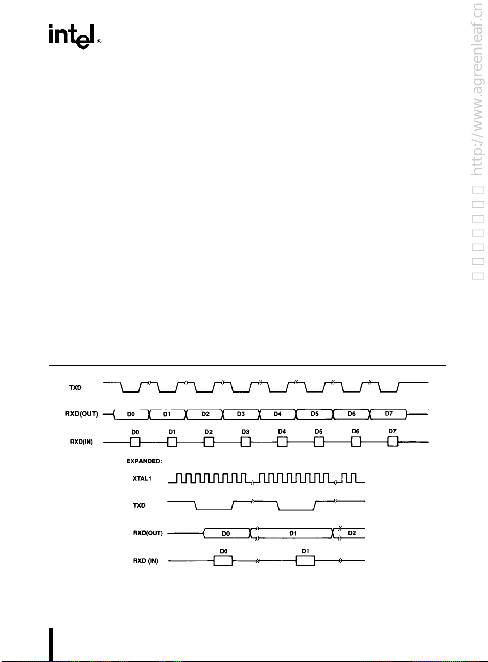
80C196KB USER’S GUIDE
数控原理与维修 http://www.agreenleaf.cn
10.2 Serial Port Interrupts
The serial port generates one of three possible interrupts: Transmit Interrupt TI(2030H), Receive Interrupt RI(2032H) and SERIAL(200CH). When the RI
bit gets set an interrupt is generated through either
200CH or 2032H depending on which interrupt is enabled. INTÐMASK1.1 controls the serial port receive
interrupt through location 2032H and INTÐMASK.6
controls serial port interrupts through location 200CH.
The 8096BH shared the TI and RI interrupts on the
SERIAL interrupt vector. On the 80C196KB, these interrupts share both the serial interrupt vector and have
their own interrupt vectors.
When the TI bit is set it can cause an interrupt through
the vectors at locations 200CH or 2030. Interrupt
through location 2030 is determined by INT
MASK1.0. Interrupts through the serial interrupt is
controlled by the same bit as the RI interrupt(INT
MASK.6). The user should not mask off the serial port
interrupt when using the double-buffered feature of the
transmitter, as it could cause a missed count in the
number of bytes being transmitted.
Ð
Ð
10.3 Serial Port Modes
MODE 0
Mode 0 is a synchronous mode which is commonly
used for shift register based I/O expansion. In this
mode the TXD pin outputs a set of 8 pulses while the
RXD pin either transmits or receives data. Data is
transferred 8 bits at a time with the LSB first. A diagram of the relative timing of these signals is shown in
Figure 10-2. Note that this is the only mode which uses
RXD as an output.
Mode 0 Timings
In Mode 0, the TXD pin sends out a clock train, while
the RXD pin transmits or receives the data. Figure 102 shows the waveforms and timing.
In this mode the serial port expands the I/O capability
of the 80C196KB by simply adding shift registers. A
schematic of a typical circuit is shown in Figure 10-3.
This circuit inverts the data coming in, so it must be
reinverted in software.
MODE 1
Mode 1 is the standard asynchronous communications
mode. The data frame used in this mode is shown in
Figure 10-4. It consists of 10 bits; a start bit (0), 8 data
bits (LSB first), and a stop bit (1). If parity is enabled
by setting SPCON.2, an even parity bit is sent instead
of the 8th data bit and parity is checked on reception.
270651– 28
Figure 10-2. Mode 0 Timing
49
Page 54

80C196KB USER’S GUIDE
数控原理与维修 http://www.agreenleaf.cn
270651– 29
Figure 10-3. Typical Shift Register Circuit
270651– 30
Figure 10-4. Serial Port Frames, Mode 1, 2, and 3
The transmit and receive functions are controlled by
separate shift clocks. The transmit shift clock starts
when the baud rate generator is initialized, the receive
shift clock is reset when a ‘1 to 0’ transition (start bit) is
received. The transmit clock may therefore not be in
sync with the receive clock, although they will both be
at the same frequency.
The TI (Transmit Interrupt) and RI (Receive Interrupt) flags are set to indicate when operations are complete. TI is set when the last data bit of the message has
been sent, not when the stop bit is sent. If an attempt to
send another byte is made before the stop bit is sent the
50
270651– 31
port will hold off transmission until the stop bit is complete. RI is set when 8 data bits are received, not when
the stop bit is received. Note that when the serial port
status register is read both TI and RI are cleared.
Caution should be used when using the serial port to
connect more than two devices in half-duplex, (i.e. one
wire for transmit and receive). If the receiving processor does not wait for one bit time after RI is set before
starting to transmit, the stop bit on the link could be
corrupted. This could cause a problem for other devices
listening on the link.
Page 55

80C196KB USER’S GUIDE
数控原理与维修 http://www.agreenleaf.cn
MODE 2
Mode 2 is the asynchronous 9th bit recognition mode.
This mode is commonly used with Mode 3 for multiprocessor communications. Figure 10-4 shows the data
frame used in this mode. It consists of a start bit (0), 9
data bits (LSB first), and a stop bit (1). When transmitting, the 9th bit can be set to a one by setting the TB8
bit in the control register before writing to SBUF (TX).
The TB8 bit is cleared on every transmission, so it must
be set prior to writing to SBUF (TX). During reception, the serial port interrupt and the Receive Interrupt
will not occur unless the 9th bit being received is set.
This provides an easy way to have selective reception
on a data link. Parity cannot be enabled in this mode.
MODE 3
Mode 3 is the asynchronous 9th bit mode. The data
frame for this mode is identical to that of Mode 2. The
transmission differences between Mode 3 and Mode 2
are that parity can be enabled (PEN
9th data bit to take the even parity value. The TB8 bit
can still be used if parity is not enabled (PEN
When in Mode 3, a reception always causes an interrupt, regardless of the state of the 9th bit. The 9th bit is
stored if PEN
e
PEN
(RPE) flag.
Mode 2 and 3 Timings
Modes 2 and 3 operate in a manner similar to that of
Mode 1. The only difference is that the data is now
made up of 9 bits, so 11-bit packages are transmitted
and received. This means that TI and RI will be set on
the 9th data bit rather than the 8th. The 9th bit can be
used for parity or multiple processor communications.
e
1 then RB8 becomes the Receive Parity Error
0 and can be read in bit RB8. If
e
1) and cause the
e
0).
10.4 Multiprocessor Communications
Mode 2 and 3 are provided for multiprocessor communications. In Mode 2 if the received 9th data bit is zero,
the RI bit is not set and will not cause an interrupt. In
Mode 3, the RI bit is set and always causes an interrupt
regardless of the value in the 9th bit. The way to use
this feature in multiprocessor systems is described below.
bit is set. Two types of frames are used: address frames
which have the 9th bit set and data frames which have
the 9th bit cleared. When the master processor wants to
transmit a block of data to one of several slaves, it first
sends out an address frame which identifies the target
slave. Slaves in Mode 2 will not be interrupted by a data
frame, but an address frame will interrupt all slaves.
Each slave can examine the received byte and see if it is
being addressed. The addressed slave switches to Mode
3 to receive the coming data frames, while the slaves
that were not addressed stay in Mode 2 continue executing.
11.0 A/D CONVERTER
Analog Inputs to the 80C196KB System are handled
by the A/D converter System. As shown in Figure
11-4, the converter system has an 8 channel multiplexer, a sample-and-hold, and a 10 bit successive approximation A/D converter. Conversions can be performed
on one of eight channels, the inputs of which share pins
with port 0. A conversion can be done in as little as 91
state times.
Conversions are started by loading the ADÐCOMMAND register at location 02H with the channel number. The conversion can be started immediately by setting the GO bit to a one. If it is cleared the conversion
will start when the HSO unit triggers it. The A/D command register must be written to for each conversion,
even if the HSO is used as the trigger. The result of
the conversion is read in the ADÐRESULT(High)
and ADÐRESULT(Low) registers. The ADÐRESULT(High) contains the most significant eight bits of
the conversion. The ADÐRESULT(Low) register contains the remaining two bits and the A/D channel number and A/D status. The format for the ADÐCOMMAND register is shown in Figure 11-1. In Window
15, reading the ADÐCOMMAND register will read
the last command written. Writing to the ADÐRESULT register will write a value into the result register.
The master processor is set to Mode 3 so it always gets
interrupts from serial receptions. The slaves are set in
Mode 2 so they only have receive interrupts if the 9th
270651– 33
Figure 11-1. A/D Command Register
51
Page 56

80C196KB USER’S GUIDE
数控原理与维修 http://www.agreenleaf.cn
The A/D converter can cause an interrupt through the
vector at location 2002H when it completes a conversion. It is also possible to use a polling method by
checking the Status (S) bit in the lower byte of the
ADÐRESULT register, also at location 02H. The
status bit will be a 1 while a conversion is in progress. It
takes 8 state times to set this bit after a conversion is
270651– 32
Figure 11-2. A/D Result Lo Register
started. The upper byte of the result register contains
the most significant 8 bits of the conversion. The lower
byte format is shown in Figure 11-2.
At high crystal frequencies, more time is needed to allow the comparator to settle. For this reason IOC2.4 is
provided to adjust the speed of the A/D conversion by
disabling/enabling a clock prescaler.
A summary of the conversion time for the two options
is shown below. The numbers represent the number of
state times required for conversion, e.g., 91 states is
22.7 ms with an 8 MHz XTAL1 (providing a 250 ns
state time.)
Clock Prescaler On Clock Prescaler Off
158 States 91 States
26.33 ms
e
IOC2.4
Figure 11-3. A/D Conversion Times
0 IOC2.4e1
@
12 MHz 22.75 m s@8 MHz.
Figure 11-4. A/D Converter Block Diagram
52
270651– 34
Page 57

80C196KB USER’S GUIDE
数控原理与维修 http://www.agreenleaf.cn
11.1 A/D Conversion Process
The conversion process is initiated by the execution of
HSO command 0FH, or by writing a one to the GO Bit
in the A/D Control Register. Either activity causes a
start conversion signal to be sent to the A/D converter
control logic. If an HSO command was used, the conversion process will begin when Timer1 increments.
This aids applications attempting to approach spectrally pure sampling, since successive samples spaced by
equal Timer1 delays will occur with a variance of about
g
50 ns (assuming a stable clock on XTAL1). However, conversions initiated by writing a one to the ADCON register GO Bit will start within three state times
after the instruction has completed execution resulting
in a variance of about 0.50 ms (XTAL1e12 MHz).
Once the A/D unit receives a start conversion signal,
there is a one state time delay before sampling (Sample
Delay) while the successive approximation register is
reset and the proper multiplexer channel is selected.
After the sample delay, the multiplexer output is connected to the sample capacitor and remains connected
for 8 state times in fast mode or 15 state times for slow
mode (Sample Time). After this 8/15 state time ‘‘sample window’’ closes, the input to the sample capacitor is
disconnected from the multiplexer so that changes on
the input pin will not alter the stored charge while the
conversion is in progress. The comparator is then autozeroed and the conversion begins. The sample delay
and sample time uncertainties are each approximately
g
50 ns, independent of clock speed.
The total number of state times required for a conversion is determined by the setting of IOC2.4 clock prescaler bit. With the bit set the conversion time is 91
states and 158 states when the bit is cleared.
11.2 A/D Interface Suggestions
The external interface circuitry to an analog input is
highly dependent upon the application, and can impact
converter characteristics. In the external circuit’s design, important factors such as input pin leakage, sample capacitor size and multiplexer series resistance from
the input pin to the sample capacitor must be considered.
For the 80C196KB, these factors are idealized in Figure 11-5. The external input circuit must be able to
charge a sample capacitor (C
) to an accurate voltage given a D.C. leakage
ance (R
I
(I
). On the 80C196KB, CSis around 2 pF, RIis
L
around 5 KX and I
determining the necessary source impedance R
value of V
BIAS
is specified as 3 mA maximum. In
L
is not important.
) through a series resist-
S
, the
S
To perform the actual analog-to-digital conversion the
80C196KB implements a successive approximation algorithm. The converter hardware consists of a 256-resistor ladder, a comparator, coupling capacitors and a
10-bit successive approximation register (SAR) with
logic that guides the process. The resistor ladder provides 20 mV steps (V
coupling creates 5 mV steps within the 20 mV ladder
e
5.12V), while capacitive
REF
voltages. Therefore, 1024 internal reference voltages are
available for comparison against the analog input to
generate a 10-bit conversion result.
A successive approximation conversion is performed by
comparing a sequence of reference voltages, to the analog input, in a binary search for the reference voltage
that most closely matches the input. The (/2 full scale
reference voltage is the first tested. This corresponds to
a 10-bit result where the most significant bit is zero,
and all other bits are ones (0111.1111.11b). If the analog input was less than the test voltage, bit 10 of the
SAR is left a zero, and a new test voltage of (/4 full scale
(0011.1111.11b) is tried. If this test voltage was lower
than the analog input, bit 9 of the SAR is set and bit 8
is cleared for the next test (0101.1111.11b). This binary
search continues until 10 tests have occurred, at which
time the valid 10-bit conversion result resides in the
SAR where it can be read by software.
270651– 35
Figure 11-5. Idealized A/D Sampling Circuitry
External circuits with source impedances of 1 KX or
less will be able to maintain an input voltage within a
tolerance of aboutg0.61 LSB (1.0 KXc3.0 mA
3.0 mV) given the D.C. leakage. Source impedances
above 2 KX can result in an external error of at least
one LSB due to the voltage drop caused by the 3 mA
leakage. In addition, source impedances above 25 KX
may degrade converter accuracy as a result of the internal sample capacitor not being fully charged during the
1 ms (12 MHz clock) sample window.
If large source impedances degrade converter accuracy
because the sample capacitor is not charged during the
sample time, an external capacitor connected to the pin
compensates for this. Since the sample capacitor is
2 pF, a 0.005 mF capacitor (2048 * 2 pF) will charge
the sample capacitor to an accurate input voltage of
g
0.5 LSB. An external capacitor does not compensate
for the voltage drop across the source resistance, but
charges the sample capacitor fully during the sample
time.
53
e
Page 58

80C196KB USER’S GUIDE
数控原理与维修 http://www.agreenleaf.cn
Placing an external capacitor on each analog input will
also reduce the sensitivity to noise, as the capacitor
combines with series resistance in the external circuit to
form a low-pass filter. In practice, one should include a
small series resistance prior to the external capacitor on
the analog input pin and choose the largest capacitor
value practical, given the frequency of the signal being
converted. This provides a low-pass filter on the input,
while the resistor will also limit input current during
over-voltage conditions.
Figure 11-6 shows a simple analog interface circuit
based upon the discussion above. The circuit in the figure also provides limited protection against over-voltage conditions on the analog input. Should the input
voltage inappropriately drop significantly below
ground, diode D2 will forward bias at about 0.8 DCV.
Since the specification of the pin has an absolute maximum low voltage of
b
0.3V, this will leave about 0.5V
across the 270X resistor, or about 2 mA of current.
This should limit the current to a safe amount.
However, before any circuit is used in an actual application, it should be thoroughly analyzed for applicability to
the specific problem at hand.
270651– 36
Figure 11-6. Suggested A/D Input Circuit
ANALOG REFERENCES
Reference supply levels strongly influence the absolute
accuracy of the conversion. For this reason, it is recommended that the ANGND pin be tied to the two V
pins at the power supply. Bypass capacitors should also
be used between V
be within about a tenth of a volt of V
be well regulated and used only for the A/D converter.
The V
needs to be able to source around 5 mA. See Section 13
supply can be between 4.5V and 5.5V and
REF
and ANGND. ANGND should
REF
SS.VREF
should
for the minimum hardware connections.
Note that if only ratiometric information is desired,
V
can be connected to VCC. In addition, V
REF
REF
and
ANGND must be connected even if the A/D converter
is not being used. Remember that Port 0 receives its
power from the V
is used as digital I/O.
and ANGND pins even when it
REF
11.3 The A/D Transfer Function
The conversion result is a 10-bit ratiometric representation of the input voltage, so the numerical value obtained from the conversion will be:
INT[1023c(V
This produces a stair-stepped transfer function when
the output code is plotted versus input voltage (see Figure 11-7). The resulting digital codes can be taken as
simple ratiometric information, or they provide information about absolute voltages or relative voltage
changes on the inputs. The more demanding the application is on the A/D converter, the more important it
is to fully understand the converter’s operation. For
simple applications, knowing the absolute error of the
converter is sufficient. However, closing a servo-loop
with analog inputs necessitates a detailed understanding of an A/D converter’s operation and errors.
The errors inherent in an analog-to-digital conversion
process are many: quantizing error, zero offset, fullscale error, differential non-linearity, and non-linearity.
These are ‘‘transfer function’’ errors related to the A/D
converter. In addition, converter temperature drift,
V
rejection, sample-hold feedthrough, multiplexer
CC
off-isolation, channel-to-channel matching and random
noise should be considered. Fortunately, one ‘‘Absolute
Error’’ specification is available which describes the
sum total of all deviations between the actual conversion process and an ideal converter. However, the various sub-components of error are important in many
applications. These error components are described in
Section 11.5 and in the text below where ideal and actual converters are compared.
An unavoidable error simply results from the conversion of a continuous voltage to an integer digital repre-
SS
sentation. This error is called quantizing error, and is
g
always
0.5 LSB. Quantizing error is the only error
seen in a perfect A/D converter, and is obviously present in actual converters. Figure 11-7 shows the transfer
function for an ideal 3-bit A/D converter (i.e. the Ideal
Characteristic).
Note that in Figure 11-7 the Ideal Characteristic possesses unique qualities: it’s first code transition occurs
when the input voltage is 0.5 LSB; it’s full-scale code
transition occurs when the input voltage equals the full-
b
IN
ANGND)/(V
REF
b
ANGND)].
54
Page 59

80C196KB USER’S GUIDE
数控原理与维修 http://www.agreenleaf.cn
270651– 37
Figure 11-7. Ideal A/D Characteristic
55
Page 60

80C196KB USER’S GUIDE
数控原理与维修 http://www.agreenleaf.cn
270651– 38
Figure 11-8. Actual and Ideal Characteristics
56
Page 61

80C196KB USER’S GUIDE
数控原理与维修 http://www.agreenleaf.cn
270651– 39
Figure 11-9. Terminal Based Characteristic
57
Page 62

80C196KB USER’S GUIDE
数控原理与维修 http://www.agreenleaf.cn
scale reference minus 1.5 LSB; and it’s code widths are
all exactly one LSB. These qualities result in a digitization without offset, full-scale or linearity errors. In other words, a perfect conversion.
Figure 11-8 shows an Actual Characteristic of a hypothetical 3-bit converter, which is not perfect. When the
Ideal Characteristic is overlaid with the imperfect characteristic, the actual converter is seen to exhibit errors
in the location of the first and final code transitions and
code widths. The deviation of the first code transition
from ideal is called ‘‘zero offset’’, and the deviation of
the final code transition from ideal is ‘‘full-scale error’’.
The deviation of the code widths from ideal causes two
types of errors. Differential Non-Linearity and NonLinearity. Differential Non-Linearity is a local linearity
error measurement, whereas Non-Linearity is an overall linearity error measure.
Differential Non-Linearity is the degree to which actual
code widths differ from the ideal one LSB width. It
gives the user a measure of how much the input voltage
may have changed in order to produce a one count
change in the conversion result. Non-Linearity is the
worst case deviation of code transitions from the corresponding code transitions of the Ideal Characteristic.
Non-Linearity describes how much Differential NonLinearities could add up to produce an overall maximum departure from a linear characteristic. If the Differential Non-Linearity errors are too large, it is possible for an A/D converter to miss codes or exhibit nonmonotonicity. Neither behavior is desirable in a closedloop system. A converter has no missed codes if there
exists for each output code a unique input voltage range
that produces that code only. A converter is monotonic
if every subsequent code change represents an input
voltage change in the same direction.
Differential Non-Linearity and Non-Linearity are
quantified by measuring the Terminal Based Linearity
Errors. A Terminal Based Characteristic results when
an Actual Characteristic is shifted and rotated to eliminate zero offset and full-scale error (see Figure 11-9).
The Terminal Based Characteristic is similar to the Actual Characteristic that would be seen if zero offset and
full-scale error were externally trimmed away. In practice, this is done by using input circuits which include
gain and offset trimming. In addition, V
80C196KB could also be closely regulated and trimmed
within the specified range to affect full-scale error.
Other factors that affect a real A/D Converter system
include sensitivity to temperature, failure to completely
reject all unwanted signals, multiplexer channel dissimilarities and random noise. Fortunately these effects are
small.
Temperature sensitivities are described by the rate at
which typical specifications change with a change in
temperature.
REF
on the
Undesired signals come from three main sources. First,
noise on V
changes on the channel being converted after the sample window has closedÐFeedthrough. Third, signals
applied to channels not selected by the multiplexerÐ
Off-Isolation.
Finally, multiplexer on-channel resistances differ slightly from one channel to the next causing Channel-toChannel Matching errors, and random noise in general
results in Repeatability errors.
CCÐVCC
Rejection. Second, input signal
11.4 A/D Glossary of Terms
Figures 11-7, 11-8, and 11-9 display many of these
terms. Refer to AP-406 ‘MCS-96 Analog Acquisition
Primer‘ for additional information on the A/D terms.
ABSOLUTE ERRORÐThe maximum difference between corresponding actual and ideal code transitions.
Absolute Error accounts for all deviations of an actual
converter from an ideal converter.
ACTUAL CHARACTERISTICÐThe characteristic of
an actual converter. The characteristic of a given converter may vary over temperature, supply voltage, and
frequency conditions. An Actual Characteristic rarely
has ideal first and last transition locations or ideal code
widths. It may even vary over multiple conversion under the same conditions.
BREAK-BEFORE-MAKEÐThe property of a multiplexer which guarantees that a previously selected
channel will be deselected before a new channel is selected. (e.g. the converter will not short inputs together.)
CHANNEL-TO-CHANNEL MATCHINGÐThe difference between corresponding code transitions of actual characteristics taken from different channels under
the same temperature, voltage and frequency conditions.
CHARACTERISTICÐA graph of input voltage versus the resultant output code for an A/D converter. It
describes the transfer function of the A/D converter.
CODEÐThe digital value output by the converter.
CODE CENTERÐThe voltage corresponding to the
midpoint between two adjacent code transitions.
CODE TRANSITIONÐThe point at which the converter changes from an output code of Q, to a code of
a
Q
1. The input voltage corresponding to a code transition is defined to be that voltage which is equally likely to produce either of two adjacent codes.
CODE WIDTHÐThe voltage corresponding to the
difference between two adjacent code transitions.
58
Page 63

80C196KB USER’S GUIDE
数控原理与维修 http://www.agreenleaf.cn
CROSSTALKÐSee ‘‘Off-Isolation’’.
D.C. INPUT LEAKAGEÐLeakage current to ground
from an analog input pin.
DIFFERENTIAL NON-LINEARITYÐThe difference between the ideal and actual code widths of the
terminal based characteristic of a converter.
FEEDTHROUGHÐAttenuation of a voltage applied
on the selected channel of the A/D converter after the
sample window closes.
FULL SCALE ERRORÐThe difference between the
expected and actual input voltage corresponding to the
full scale code transition.
IDEAL CHARACTERISTICÐA characteristic with
its first code transition at V
transition at V
widths equal to one LSB.
IN
e
(V
e
0.5 LSB, its last code
IN
b
1.5 LSB) and all code
REF
INPUT RESISTANCEÐThe effective series resistance
from the analog input pin to the sample capacitor.
LSBÐLEAST SIGNIFICANT BIT: The voltage value
corresponding to the full scale voltage divided by 2
where n is the number of bits of resolution of the converter. For a 10-bit converter with a reference voltage
of 5.12 volts, one LSB is 5.0 mV. Note that this is
different than digital LSBs, since an uncertainty of two
LSBs, when referring to an A/D converter, equals
10 mV. (This has been confused with an uncertainty of
two digital bits, which would mean four counts, or
20 mV.)
MONOTONICÐThe property of successive approximation converters which guarantees that increasing input voltages produce adjacent codes of increasing value,
and that decreasing input voltages produce adjacent
codes of decreasing value.
REPEATABILITYÐThe difference between corresponding code transitions from different actual characteristics taken from the same converter on the same
channel at the same temperature, voltage and frequency
conditions.
RESOLUTIONÐThe number of input voltage levels
that the converter can unambiguously distinguish between. Also defines the number of useful bits of information which the converter can return.
SAMPLE DELAYÐThe delay from receiving the start
conversion signal to when the sample window opens.
SAMPLE DELAY UNCERTAINTYÐThe variation
in the Sample Delay.
SAMPLE TIMEÐThe time that the sample window is
open.
SAMPLE TIME UNCERTAINTYÐThe variation in
the sample time.
SAMPLE WINDOWÐBegins when the sample capacitor is attached to a selected channel and ends when the
sample capacitor is disconnected from the selected
n
,
channel.
SUCCESSIVE APPROXIMATIONÐAn A/D conversion method which uses a binary search to arrive at
the best digital representation of an analog input.
TEMPERATURE COEFFICIENTSÐChange in the
stated variable per degree centigrade temperature
change. Temperature coefficients are added to the typical values of a specification to see the effect of temperature drift.
TERMINAL BASED CHARACTERISTICÐAn Actual Characteristic which has been rotated and translated to remove zero offset and full-scale error.
NO MISSED CODESÐFor each and every output
code, there exists a unique input voltage range which
produces that code only.
NON-LINEARITYÐThe maximum deviation of code
transitions of the terminal based characteristic from the
corresponding code transitions of the ideal characteristics.
OFF-ISOLATIONÐAttenuation of a voltage applied
on a deselected channel of the A/D converter. (Also
referred to as Crosstalk.)
V
REJECTIONÐAttenuation of noise on the V
CC
line to the A/D converter.
CC
ZERO OFFSETÐThe difference between the expected
and actual input voltage corresponding to the first code
transition.
59
Page 64

80C196KB USER’S GUIDE
数控原理与维修 http://www.agreenleaf.cn
12.0 I/O PORTS
There are five 8-bit I/O ports on the 80C196KB. Some
of these ports are input only, some are output only,
some are bidirectional and some have alternate functions. In addition to these ports, the HSI/O unit provides extra I/O lines if the timer related features of
these lines are not needed.
Port 0 is an input port which is also used as the analog
input for the A/D converter. Port 0 is read at location
0EH. Port 1 is a quasi-bidirectional port and is read or
written to through location 0FH. The three most significant bits of Port 1 are the control signals for the
HOLD
/HLDA bus port pins. Port 2 contains three
types of port lines: quasi-bidirectional, input and output. Port2 is read or written from location 10H. The
ports cannot be read or written in Window 15. The
input and output lines are shared with other functions
in the 80C196KB as shown in Figure 12-1. Ports 3 and
4 are open-drain bidirectional ports which share their
pins with the address/data bus. On EPROM and ROM
parts, Port 3 and 4 are read and written through location 1FFEH.
PIN FUNC.
2.0 Output TXD (Serial Port Transmit) IOC1.5
2.1 Input RXD (Serial Port Receive) SPCON.3
P2.2 Input EXTINT IOC1.1
2.3 Input T2CLK (Timer2 Clock & Baud) IOC0.7
2.4 Input T2RST (Timer2 Reset) IOC0.5
2.5 Output PWM Output IOC1.0
2.6 QBD* Timer2 up/down select IOC2.1
2.7 QBD* Timer2 Capture N/A
*QBDeQuasi-bidirectional
Figure 12-1. Port 2 Multiple Functions
While discussing the characteristics of the I/O pins
some approximate current or voltage specifications will
be given. The exact specifications are available in the
latest version of the data sheet that corresponds to the
part being used.
ALTERNATE CONTROL
FUNCTION REG.
In addition to acting as a digital input, each line of Port
0 can be selected to be the input of the A/D converter
as discussed in Section 11. The capacitance on these
pins is approximately 1 pF and will instantaneously increase by around 2 pF when the pin is being sampled by
the A/D converter.
Port 0 pins are special in that they may individually be
used as digital inputs and analog inputs at the same
time. A Port 0 pin being used as a digital input acts as
the high impedance input ports just described. However, Port 0 pins being used as analog inputs are required
to provide current to the internal sample capacitor
when a conversion begins. This means that the input
characteristics of a pin will change if a conversion is
being done on that pin. In either case, if Port 0 is to be
used as analog or digital I/O, it will be necessary to
provide power to this port through the V
ANGND pins.
Port 0 is only sampled when the SFR is read to reduce
the noise in the A/D converter. The data must be stable
one state time before the SFR is read.
NOTE:
*Q1 and Q2 are ESD Protection Devices
Figure 12-2. Input Port Structure
pin and
REF
270651– 76
12.1 Input Ports
Input ports and pins can only be read. There are no
output drivers on these pins. The input leakage of these
pins is in the microamp range. The specific values can
be found in the data sheet for the device being considered. Figure 12-2 shows the input port structure.
The high impedance input pins on the 80C196KB have
an input leakage of a few microamps and are predominantly capacitive loads on the order of 10 pF.
60
12.2 Quasi-Bidirectional Ports
Port 1 and Port 2 have quasi-bidirectional I/O pins.
When used as inputs the data on these pins must be
stable one state time prior to reading the SFR. This
timing is also valid for the input-only pins of Port 2 and
is similar to the HSI in that the sample occurs during
PH1 or during CLKOUT low. When used as outputs,
the quasi-bidirectional pins will change state shortly after CLKOUT falls. If the change was from ‘0’ to a ‘1’
Page 65

80C196KB USER’S GUIDE
数控原理与维修 http://www.agreenleaf.cn
表低电平导通
CHMOS Configuration. pFET 1 is turned on for 2 osc. periods after Q makes a 0-to-1 transition. During this time, pFET 1
also turns on pFET 3 through the inverter to form a latch which holds the 1. pFET 2 is also on.
Figure 12-3. CHMOS Quasi-Bidirectional Port Circuit
the low impedance pullup will remain on for one state
time after the change.
Port 1, Port 2.6 and Port 2.7 are quasi-bidirectional
ports. When the processor writes to the pins of a quasibidirectional port it actually writes into a register which
in turn drives the port pin. When the processor reads
these ports, it senses the status of the pin directly. If a
port pin is to be used as an input then the software
should write a one to its associated SFR bit, this will
cause the low-impedance pull-down device to turn off
and leave the pin pulled up with a relatively high impedance pullup device which can be easily driven down
by the device driving the input.
If some pins of a port are to be used as inputs and some
are to be used as outputs the programmer should be
careful when writing to the port.
Particular care should be exercised when using XOR
opcodes or any opcode which is a read-modify-write
instruction. It is possible for a Quasi-Bidirectional Pin
to be written as a one, but read back as a zero if an
external device (i.e., a transistor base) is pulling the pin
below V
Quasi-bidirectional pins can be used as input and output pins without the need for a data direction register.
They output a strong low value and a weak high value.
The weak high value can be externally pulled low providing an input function. Figure 12-3 shows the configuration of a CHMOS quasi-bidirectional port.
Outputting a 0 on a quasi-bidirectional pin turns on the
strong pull-down and turns off all of the pull-ups.
Whena1isoutput the pull-down is turned off and 3
pull-ups (strong-P1, weak-P3, very weak-P2) are turned
on. Each time a pin switches from 0 to 1 transistor P1
IH
.
turns on for two oscillator periods. P2 remains on until
a zero is written to the pin. P3 is used as a latch, so it is
turned on whenever the pin is above the threshold value
(around 2 volts).
To reduce the amount of current which flows when the
pin is externally pulled low, P3 is turned off when the
pin voltage drops below the threshold. The current required to pull the pin from a high to a low is at its
maximum just prior to the pull-up turning off. An external driver can switch these pins easily. The maximum current required occurs at the threshold voltage
and is approximately 700 microamps.
When the Port 1 pins are used as their alternate functions (HOLD
standard output port.
HARDWARE CONNECTION HINTS
When using the quasi-bidirectional ports as inputs tied
to switches, series resistors may be needed if the ports
will be written to internally after the part is initialized.
The amount of current sourced to ground from each
pin is typically 7 mA or more. Therefore, if all 8 pins
are tied to ground, 56 mA will be sourced. This is
equivalent to instantaneously doubling the power used
by the chip and may cause noise in some applications.
This potential problem can be solved in hardware or
software. In software, never write a zero to a pin being
used as an input.
In hardware, a 1K resistor in series with each pin will
limit current to a reasonable value without impeding
the ability to override the high impedance pullup. If all
8 pins are tied together a 120X resistor would be reasonable. The problem is not quite as severe when the
, HLDA, and BREQ), the pins act like a
270651– 40
61
Page 66

80C196KB USER’S GUIDE
数控原理与维修 http://www.agreenleaf.cn
inputs are tied to electronic devices instead of switches,
as most external pulldowns will not hold 20 mA to 0.0
volts.
Writing to a Quasi-Bidirectional Port with electronic
devices attached to the pins requires special attention.
Consider using P1.0 as an input and trying to toggle
P1.1 as an output:
ORB IOPORT1, #00000001B ; Set P1.0
; for input
XORB IOPORT1, #00000010B ; Complement
; P1.1
The first instruction will work as expected but two
problems can occur when the second instruction executes. The first is that even though P1.1 is being driven
high by the 80C196KB it is possible that it is being held
low externally. This typically happens when the port
pin drives the base of an NPN transistor which in turn
drives whatever there is in the outside world which
needs to be toggled. The base of the transistor will
clamp the port pin to the transistor’s Vbe above
ground, typically 0.7V. The 80C196KB will input this
value as a zero even if a one has been written to the port
pin. When this happens the XORB instruction will always write a one to the port pin’s SFR and the pin will
not toggle.
The second problem, which is related to the first, is that
if P1.0 happens to be driven to a zero when Port 1 is
read by the XORB instruction, then the XORB will
write a zero to P1.0 and it will no longer be useable as
an input.
The first situation can best be solved by the external
driver design. A series resistor between the port pin and
the base of the transistor often works by bringing up
the voltage present on the port pin. The second case can
be taken care of in the software fairly easily:
LDB AL, IOPORT1
XORB AL, #010B
ORB AL, #001B
STB AL, IOPORT1
A software solution to both cases is to keep a byte in
RAM as an image of the data to be output to the port;
any time the software wants to modify the data on the
port it can then modify the image byte and copy it to
the port.
If a switch is used on a long line connected to a quasibidirectional pin, a pullup resistor is recommended to
reduce the possibility of noise glitches and to decrease
the rise time of the line. On extremely long lines that
are handling slow signals, a capacitor may be helpful in
addition to the resistor to reduce noise.
12.3 Output Ports
Output pins include the bus control lines, the HSO
lines, and some of Port 2. These pins can only be used
as outputs as there are no input buffers connected to
them. The output pins are output before the rising edge
of PH1 and is valid some time during PH1. Externally,
PH1 corresponds to CLKOUT low. It is not possible to
use immediate logical instructions such as XOR to toggle these pins.
The control outputs and HSO pins have output buffers
with the same output characteristics as those of the bus
pins. Included in the category of control outputs are:
TXD, RXD (in Mode 0), PWM, CLKOUT, ALE,
BHE
,RD, and WR. The bus pins have 3 states: output
high, output low, and high impedance. Figure 12-4
shows the internal configuration of an output pin.
62
270651– 77
Figure 12-4. Output Port
Page 67

80C196KB USER’S GUIDE
数控原理与维修 http://www.agreenleaf.cn
12.4 Ports 3 and 4/AD0 –15
These pins have two functions. They are either bidirectional ports with open-drain outputs or System Bus
pins which the memory controller uses when it is accessing off-chip memory. If the EA
always act as the System Bus. Otherwise they act as bus
pins only during a memory access. If these pins are
being used as ports and bus pins, ones must be written
to them prior to bus operations.
Accessing Port 3 and 4 as I/O is easily done from internal registers. Since the LD and ST instructions require
the use of internal registers, it may be necessary to first
move the port information into an internal location before utilizing the data. If the data is already internal,
the LD is unnecessary. For instance, to write a word
value to Port 3 and 4 . . .
LD intreg, portdata ; register
ST intreg, 1FFEH ; register
To read Port 3 and 4 requires that ‘‘ones’’ be written to
the port registers to first setup the input port configuration circuit. Note that the ports are reset to this input
condition, but if zeroes have been written to the port,
then ones must be re-written to any pins which are to
line is low, the pins
w
; data
; not needed if
; already
; internal
x
; Port 3 and 4
be used as inputs. Reading Port 3 and 4 from a previously written zero condition is as follows . . .
LD intregA, #0FFFFH ; setup port
ST intregA, 1FFEH ; register
LD intregB, 1FFEH ; register
Note that while the format of the LD and ST instructions are similar, the source and destination directions
change.
When acting as the system bus the pins have strong
drivers to both V
whenever data is being output on the system bus and
are not used when data is being output by Ports 3 and
4. The pins, external input buffers and pulldowns are
shared between the bus and the ports. The ports use
different output buffers which are configured as opendrain, and require external pullup resistors. (open-drain
is the MOS version of open-collector.) The port pins
and their system bus functions are shown in Figure
12-5.
CC
; change mode
; pattern
x
; Port 3 and 4
;LD&STnot
; needed if
; previously
; written as ones
w
; Port 3 and 4
and VSS. These drivers are used
270651– 41
Figure 12-5. Port 3, 4/AD0-15 Pins
63
Page 68

80C196KB USER’S GUIDE
数控原理与维修 http://www.agreenleaf.cn
Ports 3 and 4 on the 80C196KB are open drain ports.
There is no pullup when these pins are used as I/O
ports. A diagram of the output buffers connected to
Ports 3 and 4 and the bus pins is shown in Figure 12-5.
When Ports 3 and 4 are to be used as inputs, or as bus
pins, they must first be written with a ‘1’. This will put
the ports in a high impedance mode. When they are
used as outputs, a pullup resistor must be used externally. A 15K pullup resistor will source a maximum of
0.33 milliamps, so it would be a reasonable value to
choose if no other circuits with pullups were connected
to the pin.
Ports 3 and 4 are addressed as off-chip memorymapped I/O. The port pins will change state shortly
after the falling edge of CLKOUT. When these pins are
used as Ports 3 and 4 they are open drains, their structure is different when they are used as part of the bus.
Port 3 and 4 can be reconstructed as I/O ports from the
Address/Data bus. Refer to Section 15.7 for details.
13.0 MINIMUM HARDWARE CONSIDERATIONS
The 80C196KB requires several external connections to
operate correctly. Power and ground must be connected, a clock source must be generated, and a reset circuit
must be present. We will look at each of these areas in
detail.
follow good design and board layout techniques to keep
noise to a minimum. Liberal use of decoupling caps,
and ground planes, and transient absorbers can all
V
CC
be of great help. It is much easier to design a board
with these features then to search for random noise on
a poorly designed PC board. For more information on
noise, refer to Applications Note AP-125, ‘Designing
Microcontroller Systems for Noisy Environments’ in
the Embedded Control Application Handbook.
13.3 Oscillator and Internal Timings
ON-CHIP OSCILLATOR
The on-chip oscillator circuitry for the 80C196KB, as
shown in Figure 13.1, consists of a crystal-controlled,
positive reactance oscillator. In this application, the
crystal is operated in its fundamental response mode as
an inductive reactance in parallel resonance with capacitance external to the crystal.
13.1 Power Supply
Power to the 80C196KB flows through 5 pins. V
supplies the positive voltage to the digital portion of the
chip while V
with a positive voltage. These two pins need to be connected to a 5 volt power supply. When using the A/D
converter, it is desirable to connect V
power supply, or at least a separate trace to minimize
the noise in the A/D converter.
The four common return pins, V
Angd, must all be nominally at 0 volts. Even if the
A/D converter is not being used, V
still be connected for Port0 to function.
supplies the A/D converter and Port0
REF
REF
1, VSS2, VSS3, and
SS
REF
13.2 Noise Protection Tips
Due to the fast rise and fall times of high speed CMOS
logic, noise glitches on the power supply lines and outputs at the chip are not uncommon. The 80C196KB is
no exception to this rule. So it is extremely important to
64
CC
to a separate
and Angd must
270651– 42
Figure 13-1. On-chip Oscillator Circuitry
The feedback resistor, Rf, consists of paralleled n-channel and p-channel FETs controlled by the PD (powerdown) bit. Rf acts as an open when in Powerdown
Mode. Both XTAL1 and XTAL2 also have ESD protection on the pins which is not shown in the figure.
The crystal specifications and capacitance values in
Figure 13-2 are not critical. 20 pF is adequate for any
frequency above 1 MHz with good quality crystals. Ceramic resonators can be used instead of a crystal in cost
sensitive applications. For ceramic resonators, the manufacturer should be contacted for values of the capacitors.
Page 69

270651– 43
数控原理与维修 http://www.agreenleaf.cn
Figure 13-2. External Crystal Connections
To drive the 80C196KB with an external clock source,
apply the external clock signal to XTAL1 and let
XTAL2 float. An example of this circuit is shown in
Figure 13-3. The required voltage levels on XTAL1 are
specified in the data sheet. The signal on XTAL1 must
be clean with good solid levels.
It is important that the minimum high and low times
are met to avoid having the XTAL1 pin in the transition range for long periods of time. The longer the
signal is in the transition region, the higher the probability that an external noise glitch could be seen by the
clock generator circuitry. Noise glitches on the
80C196KB internal clock lines will cause unreliable operation.
80C196KB USER’S GUIDE
INTERNAL TIMINGS
Internal operation of the chip is based on the oscillator
frequency divided by two, giving the basic time unit,
known as a ‘state time‘. With a 12 Mhz crystal, a state
time is 167 nS. Since the 80C196KB can operate at
many frequencies, the times given throughout this overview will be in state times.
Two non-overlapping internal phases are created by the
clock generator: phase 1 and phase 2 as shown in Figure 13-4. CLKOUT is generated by the rising edge of
phase 1 and phase 2. This is not the same as the
8096BH, which uses a three phase clock. Changing
from a three phase clock to a two phase one speeds up
operation for a set oscillator frequency. Consult the latest data sheet for AC timing specifications.
270651– 44
Figure 13-4. Internal Clock Phases
13.4 Reset and Reset Status
Reset starts the 80C196KB off in a known state. To
reset the chip, the RESET
least four state times after the power supply is within
tolerance and the oscillator has stabilized. As soon as
the RESET
are asynchronously driven to their reset condition.
pin is pulled low, the I/O and control pins
pin must be held low for at
Figure 13-3. External Clock Drive
270651– 78
After the RESET
sequence occurs as shown in Figure 13-5. During this
time the CCB (Chip Configuration Byte) is read from
location 2018H and stored in the CCR (Chip Configuration Register). The EA (External Access) pin qualifies whether the CCB is read from external or internal
memory. Figure 13-6 gives the reset status of all the
pins and Special Function Registers.
pin is brought high, a ten state reset
65
Page 70

80C196KB USER’S GUIDE
数控原理与维修 http://www.agreenleaf.cn
270651– 45
80C196KB Reset Sequence
66
Figure 13-5. Reset Sequence
Page 71

80C196KB USER’S GUIDE
数控原理与维修 http://www.agreenleaf.cn
WATCHDOG TIMER
There are three ways in which the 80C196KB can reset
itself. The watchdog timer will reset the 80C196KB if it
is not cleared in 64K state times. The watchdog timer is
enabled the first time it is cleared. To clear the watchdog, write a ‘1E‘ followed immediately by an ‘E1‘ to
location 0AH. Once enabled, the watchdog can only be
disabled by a reset.
Pin Multiplexed Value of the
Name Port Pins Pin on Reset
RESET Mid-sized Pullup
ALE Weak Pullup
RD Weak Pullup
BHE Weak Pullup
WR Weak Pullup
INST Weak Pullup
EA Undefined Input *
READY Undefined Input *
NMI Undefined Input *
BUSWIDTH Undefined Input *
CLKOUT Phase 2 of Clock
System Bus P3.0 –P4.7 Weak Pullups
ACH0–7 P0.0–P0.7 Undefined Input *
PORT1 P1.0–P1.7 Weak Pullups
TXD P2.0 Weak Pullup
RXD P2.1 Undefined Input *
EXTINT P2.2 Undefined Input *
T2CLK P2.3 Undefined Input *
T2RST P2.4 Undefined Input *
PWM P2.5 Weak Pulldown
Ð P2.6– P2.7 Weak Pullups
HSI0–HSI1 Undefined Input *
HSI2/HSO4 Undefined Input *
HSI3/HSO5 Undefined Input *
HSO0–HSO3 Weak Pulldown
RST INSTRUCTION
Executing a RST instruction will also reset the
80C196KB. The opcode for the RST instruction is
0FFH. By putting pullups on the Addr/data bus, unimplemented areas of memory will read 0FFH and cause
the 80C196KB to be reset.
Register Name Value
ADÐRESULT 7FF0H
HSIÐSTATUS x0x0x0x0B
SBUF(RX) 00H
INTÐMASK 00000000B
INTÐPENDING 00000000B
TIMER1 0000H
TIMER2 0000H
IOPORT1 11111111B
IOPORT2 11000001B
SPÐSTAT/SPÐCON 00001011B
IMASK1 00000000B
IPEND1 00000000B
WSR XXXX0000B
HSIÐMODE 11111111B
IOC2 X0000000B
IOC0 000000X0B
IOC1 00100001B
PWMÐCONTROL 00H
IOPORT3 11111111B
IOPORT4 11111111B
IOS0 00000000B
IOS1 00000000B
IOS2 00000000B
*These pins must be driven and not left floating.
Figure 13-6. Chip Reset Status
67
Page 72

80C196KB USER’S GUIDE
数控原理与维修 http://www.agreenleaf.cn
RESET CIRCUITS
The simplest way to reset an 80C196KB is to insert a
capacitor between the RESET
80C196KB has an internal pullup which has a value
between 6K and 50K ohms. A 5 uF or greater capacitor should provide sufficient reset time as long as Vcc
rises quickly.
Figure 13-7 shows what the RESET
ternally. The RESET
an output to reset an entire system with a watchdog
timer overflow, or by executing a RST instruction. For
a system reset application, the reset circuit should be a
one-shot with an open collector output. The reset pulse
may have to be lengthened and buffered since RESET
pin functions as an input and as
pin and VSS. The
pin looks like in-
is only asserted for four state times. If this is done, it is
possible for the 80C196KB to start running before other chips in the system are out of reset. Software must
take this condition into account. A capacitor cannot be
connected directly to RESET
pins of other chips in the circuit. The capacitor may
keep the voltage on the pin from going below guaranteed V
ure 13-8 shows an example of a system reset circuit.
for circuits connected to the RESET pin. Fig-
IL
if it is to drive the reset
13.5 Minimum Hardware Connections
Figure 13-9 shows the minimum connections needed to
get the 80C196KB up and running. It is important to
tie all unused inputs to V
or VSS. If these pins are
CC
NOTE:
1. The diode will provide a faster cycle time repetitive power-on-resets.
68
270651– 46
Figure 13-7. Reset Pin
270651– 47
Figure 13-8. System Reset Circuit
Page 73

NOTE:
数控原理与维修 http://www.agreenleaf.cn
*Must be driven high or low.
was formerly the CDE pin. The CDE function is no longer available. This pin must be connectd to VSS.
**V
SS3
Figure 13-9. 80C196KB Minimum Hardware Connections
left floating, they can float to a mid voltage level and
draw excessive current. Some pins such as NMI or
EXTINT may generate spurious interrupts if left unconnected.
14.0 SPECIAL MODES OF OPERATION
The 80C196KB has Idle and Powerdown Modes to reduce the amount of current consumed by the chip. The
80C196KB also has an ONCE (ON-Circuit-Emulation)
Mode to isolate itself from the rest of the components
in the system.
14.1 Idle Mode
The Idle Mode is entered by executing the instruction
‘IDLPD
ing. The CPU clocks are frozen at logic state zero, but
the peripheral clocks continue to be active. CLKOUT
continues to be active. Power consumption in the Idle
Mode is reduced to about 40% of the active Mode.
The CPU exits the Idle Mode by any enabled interrupt
source or a hardware reset. Since all of the peripherals
are running, the interrupt can be generated by the HSI,
HSO, A/D, serial port, etc. When an interrupt brings
Ý
1’. In the Idle Mode, the CPU stops execut-
80C196KB USER’S GUIDE
270651– 48
the CPU out of the Idle Mode, the CPU vectors to the
corresponding interrupt service routine and begins executing. The CPU returns from the interrupt service
routine to the next instruction following the ‘IDLPD
Ý
1’ instruction that put the CPU in the Idle Mode.
In the Idle Mode, the system bus control pins (ALE,
RD
,WR, INST, and BHE), go to their inactive states.
Ports 3 and 4 will retain the value present in their data
latches if being used as I/O ports. If these ports are the
ADDR/DATA bus, the pins will float.
It is important to note the Watchdog Timer continues
to run in the Idle Mode if it is enabled. So the chip
must be awakened every 64K state times to clear the
Watchdog or the chip will reset.
14.2 Powerdown Mode
The Powerdown Mode is entered by executing the instruction, ‘IDLPD
internal clocks are frozen at logic state zero and the
oscillator is shut off. All 232 bytes of registers and most
peripherals hold their values if V
Power is reduced to the device leakage and is in the uA
range. The 87C196KB (EPROM part) will consume
more power if the EPROM window is not covered.
Ý
2’. In the Powerdown Mode, all
is maintained.
CC
69
Page 74

80C196KB USER’S GUIDE
数控原理与维修 http://www.agreenleaf.cn
Figure 14-1. Power Up and Power Down Sequence
In Powerdown, the bus control pins go to their inactive
states. All of the output pins will assume the value in
their data latches. Ports 3 and 4 will continue to act as
ports in the single chip mode or will float if acting as
the ADDR/DATA bus.
To prevent accidental entry into the Powerdown Mode,
this feature may be disabled at reset by clearing bit 0 of
the CCR (Chip Configuration Register). Since the default value of the CCR bit 0 is 1, the Powerdown Mode
is normally enabled.
The Powerdown Mode can be exited by a chip reset or
a high level on the external interrupt pin. If the RESET
pin is used, it must be asserted long enough for the
oscillator to stabilize.
When exiting Powerdown with an external interrupt, a
positive level on the pin mapped to INT7 (either
EXTINT or port0.7) will bring the chip out of Powerdown Mode. The interrupt does not have to be unmasked to exit Powerdown. An internal timing circuit
ensures that the oscillator has time to stabilize before
turning on the internal clocks. Figure 14-1 shows the
power down and power up sequence using an external
interrupt.
During normal operation, before entering Powerdown
Mode, the V
pullup. The user must connect a capacitor between V
and VSS. A positive level on the external interrupt pin
starts to discharge this capacitor. The internal current
source that discharges the capacitor can sink approximately 100 uA. When the voltage goes below about 1
volt on the VPPpin, the chip begins executing code. A
1uF capacitor would take about 4 ms to discharge to 1
volt.
pin will rise to VCCthrough an internal
PP
PP
270651– 49
If the external interrupt brings the chip out of Powerdown, the corresponding bit will be set in the interrupt
pending register. If the interrupt is unmasked, the part
will immediately execute the interrupt service routine,
and return to the instruction following the IDLPD instruction that put the chip into Powerdown. If the interrupt is masked, the chip will start at the instruction
following the IDLPD instruction. The bit in the pending register will remain set, however.
All peripherals should be in an inactive state before
entering Powerdown. If the A/D converter is in the
middle of a conversion, it is aborted. If the chip comes
out of Powerdown by an external interrupt, the serial
port will continue where it left off. Make sure that the
serial port is done transmitting or receiving before entering Powerdown. The SFRs associated with the A/D
and the serial port may also contain incorrect information when returning from Powerdown.
When the chip is in Powerdown, it is impossible for the
watchdog timer to time out because its clock has
stopped. Systems which must use the Watchdog and
Powerdown, should clear the Watchdog right before
entering Powerdown. This will keep the Watchdog
from timing out when the oscillator is stabilizing after
leaving Powerdown.
14.3 ONCE and Test Modes
Test Modes can be entered on the 80C196KB by holding ALE, INST or RD
edge of RESET
use by Intel is the ONCE, or ON-Circuit-Emulation
Mode.
in their active state on the rising
. The only Test Mode not reserved for
70
Page 75

80C196KB USER’S GUIDE
数控原理与维修 http://www.agreenleaf.cn
ONCE is entered by driving ALE high, INST low and
RD
low on the rising edge of RESET. All pins except
XTAL1 and XTAL2 are floated. Some of the pins are
not truly high impedance as they have weak pullups or
pulldowns. The ONCE Mode is useful in electrically
removing the 80C196KB from the rest of the system. A
typical application of the ONCE Mode would be to
program discrete EPROMs onboard without removing
the 80C196KB from its socket.
ALE, INST, and RD
during reset. It is important that a circuit does not inadvertantly drive these signals during reset, or a Test
Mode could be entered by accident.
are weakly pulled high or low
15.0 EXTERNAL MEMORY
INTERFACING
15.1 Bus Operation
There are several different external operating modes on
the 80C196KB. The standard bus mode uses a 16 bit
multiplexed address/data bus. Other bus modes include
an 8 bit external bus mode and a mode in which the bus
size can be dynamically switched between 8-bits and
16-bits. In addition, there are several options available
on the type of bus control signals which make an external bus simple to design.
In the standard mode, external memory is addressed
through lines AD0-AD15 which form a 16 bit multiplexed bus. The address/data bus shares pins with ports
3 and 4. Figure 15-1 shows an idealized timing diagram
for the external bus signals.
Address Latch Enable (ALE) provides a strobe to
transparent latches (74AC373s) to demultiplex the bus.
To avoid confusion, the latched address signals will be
called MA0-MA15 and the data signals will be named
MD0-MD15.
The data returned from external memory must be on
the bus and stable for a specified setup time before the
rising edge of RD
the end of the sampling window. Writing to external
memory is controlled with the WR
valid on MD0-MD15 on the rising edge of WR
time data must be latched by the external system. The
80C196KB has ample setup and hold times for writes.
When BHE
high byte of the data bus is selected. When MA0 is a 0,
the memory connected to the low byte of the data bus is
selected. In this way accesses to a 16-bit wide memory
can be to the low (even) byte only (MA0e0, BHEe1),
to the high (odd) byte only (MA0
both bytes (MA0
When a block of memory is decoded for reads only, the
system does not have to decode BHE
80C196KB will discard the byte it does not need. For
systems that write to external memory, a system must
generate separate write strobes to both the high and low
byte of memory. This is discussed in more detail later.
All of the external bus signals are gated by the rising
and falling edges of CLKOUT. A zero waitstate bus
cycle consists of two CLKOUT periods. Therefore,
there are 4 clock edges that generate a complete bus
cycle. The first falling edge of CLKOUT asserts ALE
and drives an address on the bus. The rising edge of
(read). The rising edge of RD signals
(write) pin. Data is
is asserted, the memory connected to the
e
e
0, BHEe0).
1, BHEe0), or the
. At this
and MA0. The
270651– 50
Figure 15-1. Idealized Bus Timings
71
Page 76

80C196KB USER’S GUIDE
数控原理与维修 http://www.agreenleaf.cn
11001011
CLKOUT drives ALE inactive. The next falling edge
of CLKOUT asserts RD
read cycle. During a WR
and drives valid data on the bus. On the last rising
WR
edge of CLKOUT, data is latched into the 80C196KB
for a read cycle, or data is valid for a write cycle.
READY Pin
The READY pin can insert wait states into the bus
cycle for interfacing to slow memory or peripherals. A
wait state is 2 Tosc in length. Since the bus is synchronized to CLKOUT, it can only be held for an integral
number of waitstates. Because the 80C196KB is a completely static part, the number of waitstates that can be
inserted into a bus cycle is unbounded. Refer to the
next section for information on internally controlling
the number of waitstates inserted into a bus cycle.
There are several setup and hold times associated with
the READY signal. If these timings are not met, the
part may insert the incorrect number of waitstates.
INST Pin
The INST pin is useful for decoding more than 64K of
addressing space. The INST pin allows both 64K of
code space and 64K of data space. For instruction
fetches from external memory, the INST pin is asserted, or high for the entire bus cycle. For data reads and
writes, the INST pin is low. The INST pin is low for
the Chip Configuration Byte fetch and for interrupt
vector fetches.
(read) and floats the bus for a
(write) cycle, this edge asserts
15.2 Chip Configuration Register
The CCR (Chip Configuration Register) is the first
byte fetched from memory following a chip reset. The
CCR is fetched from the CCB (Chip Configuration
Byte) at location 2018H in either internal or external
memory depending on the state of the EA
CCR is only written once during the reset sequence.
Once loaded, the CCR cannot be changed until the next
reset.
The CCR is shown in Figure 15-2. The two most significant bits control the level of ROM/EPROM protection. ROM/EPROM protection is covered in the last
section. The next two bits control the internal READY
mode. The next three bits determine the bus control
signals. The last bit enables or disables the Powerdown
pin. The
Mode. Before the CCB fetch, if the program memory is
external, the CPU assumes that the bus is configured as
an 8-bit bus. In the 8-bit bus mode, during the CCB
fetch, address lines 8– 15 use only the weak drivers.
However, in a 16-bit bus system, the external memory
device will be driving the high byte of the bus while
outputting the CCB. This could cause bus contention if
location 2019H contains FFH. A value 20H in location
2019H will help prevent the contention.
270651– 51
Figure 15-2. Chip Configuration Register
READY control
To simplify ready control, four modes of internal ready
control are available. The modes are chosen by bits 4
and 5 of the CCR and are shown in Figure 15-3.
IRC1 IRC0 Description
0 0 Limit to one wait state
0 1 Limit to two wait states
1 0 Limit to three wait states
1 1 Wait states not limited internally
Figure 15-3. Ready Control Modes
The internal ready control logic limits the number of
waitstates that slow devices can insert into the bus cycle. When the READY pin is pulled low, waitstates are
inserted into the bus cycle until the READY pin goes
high, or the number of waitstate equal the number programmed into the CCR. So the ready control is a simple logical OR between the READY pin and the internal ready control.
72
Page 77

80C196KB USER’S GUIDE
数控原理与维修 http://www.agreenleaf.cn
This feature gives very simple and flexible ready control. For example, every slow memory chip select line
could be ORed together and connected to the READY
pin with Internal Ready Control programmed to insert
the desired number of waitstates into the bus cycle.
If the READY pin is pulled low during the CCR fetch,
the bus controller will automatically insert 3 waitstates
into the CCR bus cycle. This allows the CCR fetch to
come from slow memory without having to assert the
READY pin.
Bus Control
Using the CCR, the 80C196KB can generate several
types of control signals designed to reduce external
16-Bit Bus Cycle
270651– 52
Figure 15-4. Standard Bus Control
hardware. The ALE, WR, and BHE pins serve dual
functions. Bits 2 and 3 of the CCR specify the function
performed by these control lines.
Standard Bus Control
If CCR bits 2 and 3 are 1s, the standard bus control
signals ALE, WR
, and BHE are generated as shown in
Figure 15-4. ALE rises as the address starts to be driven, and falls to externally latch the address. WR
en for every write. BHE
form WRL
and WRH for even and odd byte writes.
and MA0 can be combined to
8-Bit Bus Cycle
is driv-
270651– 53
Figure 15-5. Decoding WRL and WRH
270651– 79
73
Page 78

80C196KB USER’S GUIDE
数控原理与维修 http://www.agreenleaf.cn
Figure 15-5 is an example of external circuitry to decode WRL
and WRH.
Write Strobe Mode
The Write Strobe Mode eliminates the need to externally decode for odd and even byte writes. If CCR bit 2 is
0, and the bus is a 16-bit cycle, WRL
generated in place of WR
and BHE. WRL is asserted
and WRH are
for all byte writes to an even address and all word
writes. WRH
is asserted for all byte writes to odd addresses and all word writes. The Write Strobe mode is
shown in Figure 15-6.
In the eight bit mode, WRL
and WRH are asserted for
both even and odd addresses.
Address Valid Strobe Mode
Address Valid strobe replaces ALE if CCR bit 3 is 0.
When Address valid Strobe mode is selected, ADV
will
be asserted after an external address is setup. It will
stay asserted until the end of the bus cycle as shown in
Figure 15-7. ADV
for external memory. ADV
can be used as a simple chip select
looks exactly like ALE for
back to back bus cycles. The only difference is ADV
will be inactive when the external bus is idle.
Address Valid with Write Strobe
If CCR bits 2 and 3 are 0, the Address Valid with Write
Strobe mode is enabled. Figure 15-8 shows the signals.
16-Bit Bus Cycle
16-Bit Bus Cycle
Figure 15-7. Address Valid Strobe Mode
74
270651– 55
Figure 15-6. Write Strobe Mode
270651– 57
8-Bit Bus Cycle
8-Bit Bus Cycle
270651– 56
270651– 58
Page 79

80C196KB USER’S GUIDE
数控原理与维修 http://www.agreenleaf.cn
15.3 Bus Width
The 80C196KB external bus width can be run-time
conFigured to operate as a 16 bit multiplexed address/
data bus, or as an MCS-51 style multiplexed 16 bit address/8 bit data bus.
16-Bit Bus Cycle
Figure 15-8. Address Valid with Write Strobe Mode
270651– 59
During 16 bit bus cycles, Ports 3 and 4 contain the
address multiplexed with data using ALE to latch the
address. In 8-bit bus cycles, Port 3 is multiplexed with
address/data but Port 4 only outputs the upper 8 address bits. The Addresses on Port 4 are valid throughout the entire bus cycle. Figure 15-9 shows the two bus
width options.
8-Bit Bus Cycle
270651– 60
(a) 16-Bit Bus
270651– 61
Figure 15-9. Bus Width Options
(b) 8-Bit Bus
270651– 62
75
Page 80

80C196KB USER’S GUIDE
数控原理与维修 http://www.agreenleaf.cn
11001011
The external bus width can be changed every bus cycle
if a 1 was loaded into bit CCR.1 at reset. The bus width
is changed on the fly by using the BUSWIDTH pin. If
the BUSWIDTH pin is a 1, the bus cycle is 16-bits. For
an 8-bit bus cycle, the BUSWIDTH pin is a zero. The
BUSWIDTH is sampled by the 80C196KB after the
address is on the bus. The BUSWIDTH pin has about
the same timing as the READY pin.
Applications for the BUSWIDTH pin are numerous.
For example, a system could have code fetched from 16
bit memory, while data would come from 8 bit memory. This saves the cost of using two 8 bit static RAMS if
only the capacity of one is needed. This system could be
easily implemented by tying the chip select input of the
8-bit memory to the BUSWIDTH pin.
If CCR bit 1 is a 0, the 80C196KB is locked into the 8
bit mode and the BUSWIDTH pin is ignored.
When executing code from a 8-bit bus, some performance degradation is to be expected. The prefetch queue
cannot be kept full under all conditions from an 8-bit
bus. Also, word reads and writes to external memory
will take an extra bus cycle for the extra byte.
15.4 HOLD/HLDA Protocol
The 80C196KB supports a bus exchange protocol, allowing other devices to gain control of the bus. The
protocol consists of three signals, HOLD
BREQ
. HOLD is an input asserted by a device which
requests the 80C196KB bus. Figure 15-10 shows the
timing for HOLD
by releasing the bus and asserting HLDA
device is done accessing the 80C196KB memory, it relinquishes the bus by deactivating the HOLD
80C196KB will remove its HDLA
of the bus. The third signal, BREQ
80C196KB during the hold sequence when it has a
pending external bus cycle. The 80C196KB deactivates
BREQ
at the same time it deactivates HDLA.
The HOLD
with P1.7, P1.6, and P1.5, respectively. To enable
HOLD
, HLDA and BREQ, the HLDEN bit (WSR.7)
must be 1. HLDEN is cleared during reset. Once this
bit is set, the port1 pins cannot be returned to being
quasi-bidirectional pins until the device is reset, but can
still be read. The HOLD/HLDA feature, however, can
be disabled by clearing the HLDEN bit.
The HOLD
is low.
When the 80C196KB acknowledges the hold request,
the output buffers for the addr/data bus, RD,WR,
and INST are floated. Although the strong pullup
BHE
and pulldown on ALE/ADV
down is turned on. This provides the option to wire OR
ALE with other bus masters. The request to hold latency is dependent on the state of the bus controller.
/HLDA. The 80C196KB responds
, HLDA, and BREQ pins are multiplexed
is sampled on phase 1, or when CLKOUT
are disabled, a weak pull-
, HLDA, and
. When the
pin. The
and assume control
, is asserted by the
76
270651– 63
Figure 15-10. HOLD/HLDA Timings
Page 81

80C196KB USER’S GUIDE
数控原理与维修 http://www.agreenleaf.cn
MAXIMUM HOLD LATENCY
The time between HOLD being asserted and HLDA
being driven is known as Hold Latency. After recognizing HOLD
cycle to finish, and then asserts HLDA
, the 80C196KB waits for any current bus
. There are 3
types bus cycles; 8-bit external cycle, 16-bit external
cycle, and an idle bus. Accessing on-chip
ROM/EPROM is an idle bus.
HOLD
is an asynchronous input. There are two different system configurations for asserting HOLD
80C196KB will recognize HOLD
internally on the next
clock edge if the system meets Thvch (HOLD
CLKOUT high). If Thvch is not met (HOLD
asynchronously), HOLD
may be recognized one clock
. The
valid to
applied
later (see Figure 15-12). Consult the latest 80C196KB
data sheet for the Thvch specification.
Figure 15-12 shows the 80C196KB entering HOLD
when the bus is idle. This is the minimum hold latency
for both the synchronous and asynchronous cases. If
Thvch is met, HLDA
is asserted about on the next
falling edge of CLKOUT. See the data sheet for Tclhal
(CLKOUT low to HLDA
case, the minimum hold latency
a
Tclhal.
If HOLD
hold latency increases by one state time and
a
is asserted asynchronously, the minimum
1.5 statesaTclhal.
low) specification. For this
e
Thvcla0.5 states
e
Thvcl
Figure 15-11 summarizes the additional hold latency
added to the minimum latency for the 3 types of bus
cycles. When accessing external memory, add one state
for each waitstate inserted into the bus cycle. For an
8-bit bus, worst case hold latency is for word reads or
writes. For this case, the bus controller must access the
bus twice, which increases latency by two states.
For exiting Hold, the minimum hold latency times apply for when the 80C196KB will deassert HLDA
response to HOLD
being removed.
Idle Bus Min
16-bit External Access Mina1 state
8-bit External Access Mina3 states
MineThvcla0.5 statesaTclhal if Thvcl is met
e
Thvcla1.5 statesaTclhal for asynchronous HOLD
Figure 15-11. Maximum Hold Latency
REGAINING BUS CONTROL
There is no delay from the time the 80C196KB removes HLDA
After HOLD
to the time it takes control of the bus.
is removed, the 80C196KB drops HLDA
in the following state and resumes control of the bus.
BREQ
is asserted when the part is in hold and needs to
perform an external memory cycle. An external memory cycle can be a data access or a request from the
prefetch queue for a code request. A request comes
from the queue when it contains two bytes or less. Once
asserted, it remains asserted until HOLD
At the earliest, BREQ
can be asserted with HLDA.
Hold requests do not freeze the 80C196KB when executing out of internal memory. The part continues executing as long as the resources it needs are located internal to the 80C196KB. As soon as the part needs to
access external memory, it asserts BREQ
the HOLD
to be removed. At this time, the part cannot
respond to any interrupt requests until HOLD
moved.
When executing out of external memory during a
HOLD
, the 80C196KB keeps running until the queue
is empty or it needs to perform an external data cycle.
The 80C196KB cannot service any interrupts until
HOLD
is removed.
The 80C196KB will also respond to hold requests in
the Idle Mode. The latency for entering bus hold from
the Idle Mode is the same as when executing out of
internal memory.
Special consideration must be given to the bus arbiter
design if the 80C196KB can be reset while in HOLD
For example, a CPU part would try and fetch the CCR
from external memory after RESET
Now there would be two parts attempting to access
80C196KB memory. Also, if another bus master is directly driving ALE, RD
in
or another test mode could be entered. The simplest
solution is to make the RESET
, and INST, the ONCE mode
pin of the 80C196KB a
system reset. This way the other bus master would also
be reset. Examples of system reset circuits are given in
Section 13.
is removed.
and waits for
is re-
.
is brought high.
77
Page 82

80C196KB USER’S GUIDE
数控原理与维修 http://www.agreenleaf.cn
Case 1. Meeting Thvcl
Case 2. Asserting HOLD Asynchronously
Figure 15-12. HOLD Applied Asynchronously
DISABLING HOLD
Clearing the HLDEN bit (WSR.7), can disable HOLD
requests when consecutive memory cycles are required.
Clearing the HDLEN bit, however, does not cause the
80C196KB to take over the bus immediately. The
80C196KB waits for the current HOLD
ish. Then it disables the bus hold feature, causing any
new requests to be ignored until the HLDEN bit is set
again. Since there is a delay from the time the code for
clearing this bit is fetched to the time it is actually executed, the code that clears HLDEN needs to be a few
instructions ahead of the block that needs to be protected from HOLD
REQUESTS
request to fin-
requests.
270651– 82
270651– 83
The safest way is to add a JBC instruction to check the
status of the HLDA
HLDEN bit. Figure 15-13 is an example of code that
prevents the part from executing a new instruction until
both current HOLD
feature is disabled.
pin after the code that clears the
requests are serviced and the hold
15.5 AC Timing Explanations
Figure 15-14 shows the timing of the ADDR/DATA
bus and control signals. Refer to the latest data sheet
for the AC timings to make sure your system meets
specifications. The major timing specifications are explained in Figure 15-15.
DI ; disable interrupts
WAIT: JBC PORT1, 6, WAIT; Check the HLDA pin
ANDB WSR, #OEFH ; disable hold request
#
#
#
ORB WSR,#80h ; enable HOLD requests
EI ; enable interrupts
NOTE:
Interrupts should be disabled to prevent code interruption
78
; If set, execute
; protected instructions
Figure 15-13. HOLD code
Page 83

80C196KB USER’S GUIDE
数控原理与维修 http://www.agreenleaf.cn
270651– 80
Figure 15-14. AC Timing Diagrams
79
Page 84

80C196KB USER’S GUIDE
数控原理与维修 http://www.agreenleaf.cn
Figure 15-14. AC Timing Diagrams (Continued)
80
270651– 81
270651– 84
Page 85

80C196KB USER’S GUIDE
数控原理与维修 http://www.agreenleaf.cn
TIMINGS THE MEMORY SYSTEM MUST MEET:
T
Ð ADDRESS Valid to READY Setup:
AVYV
Maximum time the memory system has
to decode READY after ADDRESS is
output by the 80C196KB to guarantee at
least one-wait state will occur.
T
Ð ALE Low to READY Setup: Maximum
LLYV
time the memory system has to decode
READY after ALE falls to guarantee at
least one wait state will occur.
T
Ð READY Low to READY HIGH: Maxi-
YLYH
mum amount of nonREADY time or
the maximum number of wait states that
can be inserted into a bus cycle. Since
the 80C196KB is a completely static
T
part, T
Ð READY Hold after CLKOUT Low:
CLYX
Minimum time the level on the READY
YLYH
is unbounded.
pin must be valid after CLKOUT falls.
The minimum hold time is always 0 ns.
If maximum value is exceeded, additional wait states will occur.
T
Ð READY Hold AFTER ALE Low: Mini-
LLYX
mum time the level on the READY pin
must be valid after ALE falls. If maximum value is exceeded, additional wait
states will occur.
T
Ð ADDRESS Valid to BUSWIDTH Val-
AVGV
id: Maximum time the memory system
has to decode BUSWIDTH after ADDRESS is output by the 80C196KB. If
exceeded, it is not guaranteed the
80C196KB will respond with an 8- or
16-bit bus cycle.
T
Ð ALE Low to BUSWIDTH Valid: Maxi-
LLGV
mum time after ALE/ADV
falls until
BUSWIDTH must be valid. If exceeded,
it is not guaranteed the 80C196KB will
respond with an 8- or 16-bit bus cycle.
T
Ð BUSWIDTH Hold after CLKOUT
CLGX
Low: Minimum time BUSWIDTH must
be held valid after CLKOUT falls. Always 0 ns of the 80C196KB.
T
Ð ADDRESS Valid to Input Data Valid:
AVDV
Maximum time the memory system has
to output valid data after the 80C196KB
outputs a valid address.
T
Ð RD Low to Input Data Valid: Maximum
RLDV
time the memory system has to output
valid data after the 80C196KB asserts
RD
.
T
Ð CLKOUT Low to Input Data Valid:
CLDV
Maximum time the memory system has
to output valid data after the CLKOUT
falls.
T
Ð RD High to Input Data Float: Time af-
RHDZ
is inactive until the memory sys-
ter RD
tem must float the bus. If this timing is
not met, bus contention will occur.
T
Ð Data Hold after RD Inactive: Time after
RXDX
RD
is inactive that the memory system
must hold Data on the bus. Always 0 ns
on the 80C196KB.
TIMINGS THE 80C196KB WILL PROVIDE:
F
Ð Frequency on XTAL1: Frequency of sig-
XTAL
nal input into the 80C196KB. The
80C196KB runs internally at (/2 F
T
T
Ð 1/F
OSC
XHCH
enced to T
Ð XTAL1 High to CLKOUT High or
Low: Needed in systems where the sig-
: All A.C. Timings are refer-
XTAL
OSC
.
nal driving XTAL1 is also a clock for
external devices.
T
T
Ð CLKOUT Cycle Time: Nominally 2
CLCL
CHCL
T
.
OSC
Ð CLKOUT High Period: Needed in sys-
tems which use CLKOUT as clock for
external devices.
T
T
T
T
Ð CLKOUT Falling Edge to ALE/ADV
CLLH
LLCH
LHLH
LHLL
Rising: A help in deriving other timings.
Ð ALE/ADV Falling Edge to CLKOUT
Rising: A help in deriving other timings.
Ð ALE Cycle Time: Time between ALE
pulses.
Ð ALE/ADV High Period: Useful in de-
termining ALE/ADV
rising edge to
ADDRESS valid. External latches must
also meet this spec.
T
Ð ADDRESS Setup to ALE/ADV Falling
AVLL
Edge: Length of time ADDRESS is valid before ALE/ADV
falls. External
latches must meet this spec.
T
Ð ADDRESS Hold after ALE/ADV Fall-
LLAX
ing Edge: Length of Time ADDRESS is
valid after ALE/ADV
falls. External
latches must meet this spec.
T
Ð ALE/ADV Low to RD Low: Length of
LLRL
time after ALE/ADV
falls before RD is
asserted. Could be needed to insure
proper memory decoding takes place before a device is enabled.
XTAL
.
Figure 15-15. AC Timing Explanations
81
Page 86

80C196KB USER’S GUIDE
数控原理与维修 http://www.agreenleaf.cn
T
RLCL
T
RLRH
T
RHLH
T
RLAZ
T
LLWL
T
CLWL
T
QVWH
T
CHWH
Ð RD Low to CLKOUT Falling Edge:
Length of time from RD
asserted to
CLKOUT falling edge: Useful for systems based on CLKOUT.
Ð RD Low to RD High: RD pulse width.
Ð RD High to ALE/ADV Asserted: Time
between RD
ALE/ADV
going inactive and next
, also used to calculate time
between inactive and next ADDRESS
valid.
Ð RD Low to ADDRESS Float: Used to
calculate when the 80C196KB stops
driving ADDRESS on the bus.
Ð ALE/ADV Low Edge to WR Low:
Length of time ALE/ADV
is asserted. Could be needed to en-
WR
falls before
sure proper memory decoding takes
place before a device is enabled.
Ð CLKOUT Falling Edge to WR Low:
Time between CLKOUT going low and
WR
being asserted. Useful in systems
based on CLKOUT.
Ð Data Valid to WR Rising Edge: Time
between data being valid on the bus and
going inactive. Memory devices
WR
must meet this spec.
Ð CLKOUT High to WR Rising Edge:
Time between CLKOUT going high and
WR
going inactive. Useful in systems
based on CLKOUT.
T
WLWH
T
WHQX
T
WHLH
T
WHBX
T
RHBX
T
WHAX
T
RHAX
Ð WR Low to WR High: WR pulse width.
Memory devices must meet this spec.
Ð Data Hold after WR Rising Edge:
Amount of time data is valid on the bus
after WR
going inactive. Memory devic-
es must meet this spec.
Ð WR Rising Edge to ALE/ADV
Edge: Time between WR
and next ALE/ADV
culate WR
inactive and next ADDRESS
. Also used to cal-
Rising
going inactive
valid.
Ð BHE, INST, Hold after WR Rising
Edge: Minimum time these signals will
be valid after WR
inactive.
Ð BHE, INST HOLD after RD Rising
Edge: Minimum time these signals will
be valid after RD
inactive.
Ð AD8 –15 Hold after WR Rising Edge:
Minimum time the high byte of the address in 8-bit mode will be valid after
WR
inactive.
Ð AD8 –15 Hold after RD Rising Edge:
Minimum time the high byte of the address in 8-bit mode will be valid after
RD
inactive.
Figure 15-15. AC Timing Explanations (Continued)
Figure 15-16. 8-Bit System with EPROM
82
270651– 66
Page 87

80C196KB USER’S GUIDE
数控原理与维修 http://www.agreenleaf.cn
15.6 Memory System Examples
External memory systems for the 80C196KB can be set
up in many different ways. Figure 15-16 shows a simple
8 bit system with a single EPROM. The ADV
can be selected to provide a chip select to the memory.
By setting bit CCR.1 to 0, the system is locked into the
eight bit mode. An eight bit system with EPROM and
RAM is shown in Figure 15-17. The EPROM is decod-
Figure 15-17. 8-Bit System with EPROM and RAM
Mode
ed in the lower half of memory,and the RAM in the
upper half.
Figure 15-18 shows a 16 bit system with 2 EPROMs.
Again, ADV
15-19 shows a system with dynamic bus width. Code is
executed from the two EPROMs and data is stored in
the single RAM. Note the Chip Select of the RAM also
is input to the BUSWIDTH pin to select an eight bit
cycle.
is used to chip select the memory. Figure
270651– 67
Figure 15-18. 16-Bit System with EPROM
270651– 68
83
Page 88

80C196KB USER’S GUIDE
数控原理与维修 http://www.agreenleaf.cn
Figure 15-19. 16-Bit System with Dynamic Buswidth
270651– 69
Figure 15-20. I/O Port Reconstruction
84
270651– 70
Page 89

80C196KB USER’S GUIDE
数控原理与维修 http://www.agreenleaf.cn
15.7 I/O Port Reconstruction
When a single-chip system is being designed using a
multiple chip system as a prototype, it may be necessary to reconstruct I/O Ports 3 and 4 using a memory
mapped I/O technique. The circuit to reconstruct the
Ports is shown in Figure 15-20. It can be attached to a
80C196KB system which has the required address decoding and bus demultiplexing.
The output circuitry is a latch that operates when
1FFEH or 1FFFH are placed on the MA lines. The
inverters surrounding the latch create an open-collector
output to emulate the open-drain output found on the
80C196KB. The RESET
line sets the ports to all 1s
when the chip is reset. The voltage and current specifications of the port will be different from the
80C196KB, but the functionality will be the same.
The input circuitry is a bus transceiver that is addressed
at 1FFEH and 1FFFH. If the ports are going to be
either inputs or outputs, but not both, some of the circuitry may be eliminated.
16.0 USING THE EPROM
The 87C196KB contains 8 Kbytes of ultraviolet Erasable and electrically Programmable Read Only Memory (EPROM). When EA
located at memory locations 2000H through 3FFFH.
Applying
a
12.75V to EA when the chip is reset places
the 87C196KB device in the EPROM Programming
Mode. The Programming Mode supports EPROM programming and verification. The following is a brief description of each of the programming modes:
The Auto Configuration Byte Programming Mode
programs the Programming Chip Configuration Byte
and the Chip Configuration Byte.
The Auto Programming Mode enables an
87C196KB to program itself without using an
EPROM programmer.
The Slave Programming Mode provides a standard
interface for programming any number of
87C196KB’s by a master device such as an EPROM
programmer.
is a TTL high, the EPROM is
The Run-Time Programming Mode allows individual EPROM locations to be programmed at run-time
under complete software control. (Run-Time Programming is done with EA
e
5V.)
In the Programming Mode some I/O pins have new
functions. These pins determine the programming function, provide programming control signals and slave ID
numbers, and pass error information. Figure 16-1
shows how the pins are renamed. Figure 16-2 describes
each new pin function.
PMODE selects the programming mode (see Figure
16-3). The 87C196KB does not need to be in the Programming Mode to do run-time programming; it can be
done at any time.
When an 87C196KB EPROM device is not being
erased the window must be covered with an opaque
label. This prevents functional degradation and data
loss from the array.
16.1 Power-Up and Power-Down
To avoid damaging devices during programming, follow these rules:
Ý
RULE
RULE
RULEÝ3VPPmust not have a low impedance path
RULE
RULE
RULE
RULE
To adhere to these rules you can use the following power-up and power-down sequences:
1VPPmust be within 1V of VCCwhile V
is below 4.5V.
Ý
2VPPcan not be higher than 5.0V until V
is above 4.5V.
to ground when V
Ý
4EAmust be brought to 12.75V before V
is above 4.5V.
CC
is brought to 12.75V (not needed for runtime programming).
Ý
5 The PMODE and SID pins must be in
their desired state before RESET rises.
Ý
6 All voltages must be within tolerance and
the oscillator stable before RESET rises.
Ý
7 The supplies to VCC,VPP,EAand RE-
SET must be well regulated and free of
spikes and glitches.
CC
CC
PP
85
Page 90

80C196KB USER’S GUIDE
数控原理与维修 http://www.agreenleaf.cn
POWER-UP
RESETe0V
e
eEAe
V
V
CC
CLOCK on (if using an external clock instead of the
internal oscillator)
PALE
SID and PMODE valid
EA
V
WAIT (wait for supplies and clock to settle)
RESET
PP
e
PROGePORT3, 4eV
12.75V
12.75V
e
5V
(2)
(3)
PP
e
e
WAIT Tshll (RESET high to first PALE
BEGIN
POWER-DOWN
e
RESET
V
PP
0V
e
5V
5V
IH
(1)
low)
e
5V
EA
e
PALE
0V
V
CLOCK OFF
1. V
2. The same power supply can be used for EA
V
V
from noise to prevent damage to it.
3. Exceeding the maximum limit on V
amount of time could damage the device permanently.
The V
glitches.
PROGeSIDePMODEePORT3, 4
e
eEAe
V
CC
PP
e
logical ‘‘1’’ (2.4V minimum)
IH
. However, the EA pin must be powered up before
PP
is powered up. Also, EA should be protected
PP
source must be well regulated and free of
PP
0V
NOTES:
PP
for any
and
16.2 Reserved Locations
All Intel Reserved locations except address 2019H,
when mapped internally or externally, must be loaded
with 0FFH to ensure compatibility with future devices.
Address 2019H must be loaded with 20H.
e
Figure 16-1. Programming Mode Pin Functions
86
270651– 71
Page 91

80C196KB USER’S GUIDE
数控原理与维修 http://www.agreenleaf.cn
Mode Name Function
General
Auto PCCB PVER Program Verification Output. A high signal indicates that the bytes
Programming Mode (P2.0)
Auto Programming
Mode
Slave Programming
Mode
PMODE
(P0–0.4, 0.5,
0.6, 0.7)
PALE Programming ALE Input. Indicates that Port3 contains the data to be
(P2.1)
PACT
(P2.7)
PVAL
(P3.0)
Ports
3 and 4
SID
(HSI–0.0,
0.1, 0.2, 0.3)
PALE
(P2.1)
PROG
(P2.2)
PVER
(P2.0)
AINC
(P2.4)
Ports Address/Command/Data Bus. Used to pass commands, addresses,
3 and 4
Figure 16-2. Programming Mode Pin Definitions
Programming Mode Select. Determines the EPROM programming
algorithm that is performed. PMODE is sampled after a chip reset and
should be static while the part is operating.
have programmed correctly.
programmed into the CCB and the PCCB.
Programming Active Output. Indicates when programming activity is
complete.
Program Valid Output. Indicates the success or failure of
programming. A zero indicates successful programming.
Address/Command/Data Bus. Used in the Auto Programming Mode
as a regular system bus to access external memory. Should have
pullups to V
Slave ID Number. Used to assign a pin of Port 3 or 4 to each slave to
use for passing programming verification acknowledgement. For
example, if gang programming in the Slave Programming Mode, the
slave with SID
program verification.
Programming ALE Input. Indicates that Ports 3 and 4 contain a
command/address.
Programming Input. Falling edge indicates valid data on PBUS and the
beginning of programming. Rising edge indicates end of programming.
Program Verification Output. Low signal after rising edge of PROG
indicates programming was not successful.
Auto Increment Input. Active low input signal indicates that the auto
increment mode is enabled. Auto Increment will allow reading or
writing of sequential EPROM locations without address transactions
across the PBUS for each read or write.
and data to and from 87C196KBs in the Slave Programming Mode.
One pin each can be assigned to up to 15 slaves to pass verification
information.
(15 kX).
CC
e
001 will use Port 3.1 to signal correct or incorrect
PMODE Programming Mode
0–4 Reserved
5 Slave Programming
6 ROM Dump
7–0BH Reserved
0CH Auto Programming
0DH Program Configuration Byte
0EH–0FH Reserved
Figure 16-3. Programming
Function Pmode Values
16.3 Programming Pulse Width Register (PPW)
In the Auto and Run-Time Programming Modes the
width of the programming pulse is determined by the 8
bit PPW (Programming Pulse Width) register. In the
Auto Programming Mode, the PPW is loaded from location 4014H in external memory. In Run-time Programming Mode, the PPW is located in window 14 at
04H. In order for the EPROM to properly program,
the pulse width must be set to approximately 100 uS.
The pulse width is dependent on the oscillator frequency and is calculated with the following formula:
Pulse WidthePPW * (Tosc * 8)
e
150@12 Mhz
PPW
In the Slave Programming Mode the width of the programming pulse is determined by the PROG
signal.
87
Page 92

80C196KB USER’S GUIDE
数控原理与维修 http://www.agreenleaf.cn
16.4 Auto Configuration Byte Programming Mode
The Programming Chip Configuration Byte (PCCB) is
a non-memory mapped EPROM location. It gets loaded into the CCR during reset for auto and slave programming. The Auto Configuration Byte Programming
Mode programs the PCCB.
The Chip Configuration Byte (CCB) is at location
2018H and can be programmed like any other EPROM
location using Auto, Slave, or Run-Time Programming.
However, you can also use Auto Configuration Byte
Programming to program the CCB when no other locations need to be programmed. The CCB is programmed
with the same value as the PCCB.
The Auto Configuration Byte Programming Mode is
entered by following the power-up sequence described
in Section 16.1 with PMODE
0FFH, and Port 3ethe data to be programmed into
the PCCB and CCB. When a 0 is placed on PALE the
CCB and PCCB are automatically programmed with
the data on Port 3. After programming, PVER is driven high if the bytes programmed correctly and low if
they did not.
Once the PCCB and CCB are programmed, all programming activities and bus operations use the selected
bus width, READY control, bus controls, and READ/
WRITE protection until you erase the device. You
must be careful when programming the READ and
WRITE lock bits in the PCCB and CCB. If the READ
e
0DH, Port 4
e
or WRITE lock bits are enabled, some programming
modes will require security key verification before executing and some modes will not execute. See Figure
16-10 and the sections on each programming mode for
details of the effects of enabling the lock bits.
If the PCCB is not programmed, the CCR will be loaded with 0FFFH when the device is in the Programming
Mode.
16.5 Auto Programming Mode
The Auto Programming Mode provides the ability to
program the 87C196KB EPROM without using an
EPROM programmer. For this mode follow the powerup sequence described in Section 16.1 with PMODE
0CH. External location 4014H must contain the PPW.
When RESET rises, the 87C196KB automatically programs itself with the data found at external locations
4000H through 5FFFH.
The 87C196KB begins programming by setting PACT
low. Then it reads a word from external memory. The
Modified Quick-Pulse Programming Algorithm (described later) programs the corresponding EPROM location. Since the erased state of a byte is 0FFH, the
Auto Programming Mode will skip locations with
0FFH for data. When all 8K have been programmed,
PACT
goes high and the device outputsa0onPVAL
(P3.0) if it programmed correctly and a 1 if it failed.
Figure 16-4 shows a minimum configuration using an
c
8K
8 EPROM to program an 87C196KB in the
Auto Programming Mode.
e
NOTES:
Tie Port 3 to the value desired to be programmed into
CCB and PCCB.
Make all necessary minimum connections for power,
ground and clock.
Figure 16-5. The PCCB Programming Mode
88
270651– 73
AUTO PROGRAMMING MODE AND THE
CCB/PCCB
In the Auto Programming Mode the CCR is loaded
with the PCCB. The PCCB must correspond to the
memory system of the programming setup, including
the READY and bus control selections. You can program the PCCB using the Auto Configuration Byte
Programming Mode (see Section 16.4).
The data in the PCCB takes effect upon reset. If you
enable the READ and WRITE lock bits during Auto
Programming but do not reset the device, Auto Programming will continue. If you enable either the
READ or WRITE lock bits in the CCB using Auto
Configuration Byte Programming and then reset the
87C196KB for Auto Programming, the device does a
security key verification. The same security keys that
reside at internal addresses 2020H– 202FH must reside
at external locations 4020H –402FH. If the keys match,
auto programming continues. If the keys do not match,
the device enters an endless loop of internal execution.
Page 93

NOTES:
数控原理与维修 http://www.agreenleaf.cn
*Inputs must be driven high or low.
**Allow RESET to rise after the voltages to V
Figure 16-4. Auto Programming Mode
,EA, and VPPare stable.
CC
80C196KB USER’S GUIDE
270651– 72
89
Page 94

80C196KB USER’S GUIDE
数控原理与维修 http://www.agreenleaf.cn
16.6 Slave Programming Mode
Any number of 87C196KBs can be programmed by a
master programmer through the Slave Programming
Mode. There is no 87C196KB dependent limit to the
number of devices that can be programmed.
In this mode, the 87C196KB programs like a simple
EPROM device and responds to three different commands: data program, data verify, and word dump. The
87C196KB uses Ports 3 and 4 and five other pins to
select commands, to transfer data and addresses, and to
provide handshaking. The two most significant bits on
Ports 3 and 4 specify the command and the lower 14
bits contain the address. The address ranges from
2000H-3FFFH and refers to internal memory space.
Figure 16-6 is a list of valid Programming Commands.
P4.7 P4.6 Action
0 0 Word Dump
0 1 Data Verify
1 0 Data Program
1 1 Reserved
Figure 16-6. Slave Programming
Mode Commands
The 87C196KB receives an input signal, PALE
dicate a valid command is present. PROG
87C196KB to read in or output a data word. PVER
indicates if the programming was successful. AINC
tomatically increments the address for the Data Program and Word Dump commands.
Data Program Command
A Data Program Command is illustrated in Figure 16-
7. Asserting PALE latches the command and address
on Ports 3 and 4. PROG
present on Ports 3 and 4. PROG
programming sequence. The width of the PROG
determines the programming pulse width. Note that the
PPW is not used in the Slave Programming Mode.
After the rising edge of PROG
verify the contents of the location just programmed.
PVER is asserted if the location programmed correctly.
This gives verification information to programmers
which can not use the Data Verify Command. The
AINC
pin can increment to the next location or a new
Data Program Command can be issued.
is asserted to latch the data
also starts the actual
, the slaves automatically
,toin-
causes the
au-
pulse
Figure 16-7. Data Program Command in Slave Mode
90
270651– 74
Page 95

80C196KB USER’S GUIDE
数控原理与维修 http://www.agreenleaf.cn
PVER is a 1 if the data program was successful. PVER
isa0ifthedata program was unsuccessful. Figure 16-7
shows the relationship of PALE
the Command/Data path on Ports 3 and 4 for the Data
Program Command.
Data Verify Command
When the Data Verify Command is sent, the slaves indicate correct or incorrect verification of the previous
Data Program Command by driving one bit of Ports 3
and 4. A 1 indicates a correct verification, and a 0 indicates incorrect verification. The SID (Slave I.D) of each
slave determines which bit of Ports 3 and 4 will be
driven. For example, a SID of 0001 would drive Port
3.1. PROG
ure 16-8 shows the relationship of ports 3 and 4 to
PALE
A Data Verify Command is always preceded by a Data
Program Command in a programming system with as
many as 16 slaves. However, a Data Verify Command
does not have to follow every Data Program Command.
Word Dump Command
When the Word Dump Command is issued, the
87C196KB adds 2000H to the address field of the com-
governs when the slaves drive the bus. Fig-
and PROG.
, PROG, and PVER to
mand and places the value at the new address on Ports
3 and 4. For example, when the slave receives the command 0100H, it will place the word at internal address
2100H on Ports 3 and 4. PROG
drives the bus. The Timings are the same as shown in
Figure 16-7.
Note that the Word Dump Command only works when
a single slave is attached to the bus. Also, there is no
restriction on commands that precede or follow a Word
Dump Command.
Gang Programming With the Slave
Programming Mode
Gang Programming of 87C196KBs can be done using
the Slave Programming Mode. There is no 87C196KB
based limit on the number of devices that may be
hooked to the same Port 3 and 4 data path for gang
programming.
If more than 16 devices are being gang programmed,
the PVER outputs of each chip can be used for verification. The master programmer can issue a Data Program Command, then either watch every device’s error
signal, or AND all the signals together to form a system PVER.
governs when the slave
Figure 16-8. Ports 3 and 4 to PALE and PROG
270651– 75
91
Page 96

80C196KB USER’S GUIDE
数控原理与维修 http://www.agreenleaf.cn
If 16 or fewer 87C196KBs are to be gang programmed
at once, a more flexible form of verification is available
by giving each device a unique SID. The master programmer can issue a Data Verify Command after the
Data Program Command. When a verify command is
seen by the slaves, each will drive a bit of Ports 3 or 4
corresponding to its unique SID. A 1 indicates the address verified, while a 0 means it failed.
SLAVE PROGRAMMING MODE AND THE
CCB/PCCB
Devices in the Slave Programming Mode use Ports 3
and 4 as the command/data path. The data bus is not
used. Therefore, you do not need to program either the
CCB or the PCCB before starting slave programming.
You can program the CCB like any other location in
slave mode. Data programmed into the CCB takes effect upon reset. If you enable either the READ or the
WRITE lock bits in the CCB during slave programming and do not reset the device, slave programming
will continue. If you do reset the device, the device first
does a security key verification. The same security keys
that reside at internal addresses 2020H –202FH must
reside at external addresses 4020H– 402FH. If the keys
match, slave programming continues. If the keys do not
match, the device enters an endless loop of internal execution.
LD WSR,#14 ;Initialize programmable
LD PPW,#VALUE ;pulse width
16.7 Run-Time Programming
The 87C196KB can program itself under software control. One byte or word can be programmed instead of
the entire array. The only additional requirement is
that you apply a programming voltage to V
the ambient temperature at 25
ming is done with EA
enabled).
To Run-Time Program, the user writes to the location
to be programmed. The value of the PPW register determines the programming pulse. To ensure 87C196KC
compatibility, the Idle Mode should be used for RunTime Programming. Figure 16-9 is the recommended
code sequence for Run-Time Programming. The Modified Quick Pulse algorithm guarantees the programmed
EPROM cell for the life of the part.
RUN-TIME PROGRAMMING AND THE
CCB/PCCB
For run-time programming, the CCR is loaded with the
CCB. Run-time programming is done with EA
a TTL-high (internal execution) so the internal CCB
must correspond to the memory system of the application setup. You can use Auto Configuration Byte Programming or a generic programmer to program the
CCB before using Run-Time Programming.
at a TTL high (internal memory
C. Run-time program-
§
and have
PP
equal to
PROGRAM: POP ADDRESS
LOOP: ST DATA
NOTE:
*Not Really Needed on Current 87C196KB Part
92
POP DATA
PUSHF
LD COUNT, #25T
TEMP,[ADDR TEMP] ;begin programming
DJNZ COUNT, L00P ;loop 25 times
POPF
RET
Figure 16-9. Future Run-Time Programming Algorithm
TEMP ;Load program data
TEMP ;and address
;enter idle mode
Page 97

80C196KB USER’S GUIDE
数控原理与维修 http://www.agreenleaf.cn
The CCB can also be programmed during Run-Time
Programming like any other EPROM location.
Data programmed into the CCB takes effect immediately. If the WRITE lock bit of the CCB is enabled, the
array can no longer be programmed. You should only
program the WRITE lock bit when no further programming will be done to the array. If the READ lock
bit is programmed the array can still be programmed
using run-time programming but a data access will only
be performed when the program counter is between
2000H and 3FFFH.
16.8 ROM/EPROM Memory Protection Options
Write protection is available for EPROM parts, and
read protection is provided for both ROM and
EPROM parts.
Write protection is enabled by clearing the LOC0 bit in
the CCR. When write protection is enabled, the bus
controller will cycle through the write sequence but will
not actually drive data to the EPROM or enable V
the EPROM. This protects the entire EPROM (locations 2000H –3FFFH) from inadvertent or unauthorized programming.
Read protection is enabled by clearing the LOC1 bit of
the CCR. When read protection is selected, the bus
controller will only perform a data read from the address range 2020H-202FH (Security Key) and 2040H3FFFH if the Slave Program Counter is in the range
2000H-3FFFH. Since the Slave PC can be as many as 4
bytes ahead of the CPU program counter, an instruction after address 3FFAH may not access protected
memory. Also note the interrupt vectors and CCB are
not read protected.
EA
is latched on reset so the device cannot be switched
from internal to external memory by toggling EA
PP
.
CCB.1 CCB.0
RD WR Protection
Lock Lock
1 1 Array is unprotected. ROM
0 1 Array is READ protected. Run-
1 0 Array is WRITE protected. Auto,
0 0 Array is READ and WRITE
to
ROM DUMP MODE
You can use the security key and ROM Dump Mode to
dump the internal ROM/EPROM for testing purposes.
The security key is a 16 byte number. The internal
ROM/EPROM must contain the security key at locations 2020H–202FH. The user must place the same
security key at external address 4020H –402FH. Before
doing a ROM dump, the device checks that the keys
match.
Dump Mode and all
programming modes are
allowed.
time programming is allowed.
Auto, Slave, and ROM Dump
Mode are allowed after security
key verification.
Slave, and ROM Dump Mode
are allowed after security key
verification. Run-time
programming is not allowed.
protected. Auto, Slave, and
ROM Dump Mode are allowed
after security key verification.
Run-time programming is not
allowed.
Figure 16-10
If the CCR has any protection enabled, the security key
is write protected to keep unauthorized users from overwriting the key with a known security key.
NOTE:
Substantial effort has been made to provide an excellent program protection scheme. However, Intel cannot and does not guarantee that these protection
methods will always prevent unauthorized access.
93
Page 98

80C196KB USER’S GUIDE
数控原理与维修 http://www.agreenleaf.cn
For the 87C196KB, the ROM dump mode is entered
like the other programming modes described in Section
16.1 with PMODE equal to 6H. For the 83C196KB,
the ROM Dump Mode is entered by placing EA
TTL high, holding ALE
high on the rising edge of RESET. The device first
RD
low and holding INST and
at a
verifies the security key. If the security keys do not
match, the device puts itself into an endless loop of
internal execution. If the keys match, the device dumps
internal locations 2000H-3FFFH to external locations
4000H–5FFFH.
16.9 Algorithms
The Modified Quick-Pulse Algorithm
The Modified Quick-Pulse Algorithm must be used to
guarantee programming over the life of the EPROM in
Run-time and Slave Programming Modes.
The Modified Quick-Pulse Algorithm calls for each
EPROM location to receive 25 separate 100 uS (
ms) programming cycles. Verification is done after the
25th pulse. If the location verifies, the next location is
programmed. If the location fails to verify, the location
fails the programming sequence.
Once all locations are programmed and verified, the
entire EPROM is again verified.
Programming of 87C196KB EPROMs is done with
e
V
12.75Vg0.25V and V
PP
CC
e
5.0Vg0.5V.
Signature Word
The 87C196KB contains a signature word at location
2070H. The word can be accessed in the Slave Mode by
executing a Word Dump Command. The programming
voltages are determined by reading the test ROM at
locations 2072H and 2073H. The voltages are calculated by using the following equation.
Voltagee20/256 * (test ROM data)
g
Description Location Value
Signature Word 2070H 897CH
Programming V
Programming V
CC
PP
2072H 040H
2073H 0A3H
Figure 16-10. Signature Word and Voltage Levels
Erasing the 87C196KB
After each erasure, all bits of the 87C196KB are logical
1s. Data is introduced by selectively programming 0s.
The only way to changea0toa1isbyexposure to
ultraviolet light.
Erasing begins upon exposure to light with wavelengths
shorter than approximately 4000 Angstroms. It should
be noted that sunlight and certain types of fluorescent
lamps have wavelengths in the 3000-4000 Angstrom
range. Constant exposure to room level fluorescent
5
lighting could erase an 87C196KB in about 3 years. It
would take about 1 week in direct sunlight to erase an
87C196KB.
Opaque labels should always be placed over the window to prevent unintentional erasure. In the Powerdown Mode, the part will draw more current than normal if the EPROM window is exposed to light.
The recommended erasure procedure for the
87C196KB is exposure to ultraviolet light which has a
wavelength of 2537 Angstroms. The integrated dose
(UV intensity * exposure time) should be a minimum of
15 Wsec/cm
2
. The total time for erasure is about 15 to
20 minutes at this level of exposure. The 87C196KB
should be placed within 1 inch of the lamp during exposure. The maximum integrated dose an 87C196KB can
be exposed to without damage is 7258 Wsec/cm2(1
@
12000 uW/cm2). Exposure to UV light greater
week
than this can cause permanent damage.
(5.0V)
(12.75V)
The values for the signature word and voltage levels are
shown in Figure 16-10.
94
 Loading...