

Page 1

Intel 186 EB/EC
Evaluation Board
User’s Manual
80C186EC/80C188EC
80L186EC/80L188EC
and
80C186EB/80C188EB
80L186EB/80L188EB
March 1997
Order Number: 272986-001
Page 2

Informa t ion in this do cument is provided in connection with Intel pr od ucts. No license, expre ss or implied, b y e st oppel or oth er -
wise, to any intellec t ual property r i g ht s is granted by t his document. Exc ept as provide d i n In t el’s Terms and Conditions of Sale
for such products, Intel assumes no liability whatsoever, and Intel disclaims any express or implied warranty, relating to sale
and/or u se o f In tel pro du cts i nc lud in g li abil it y o r war ra nti es r el ati ng t o fi t ness fo r a part ic ular pur pose , m ercha nta bi lit y, or i nfr i ngement of any patent, copyright or other intellectual property right. Intel products are not intended for use in medical, life saving,
or life sustaining applications.
The product may contain design defects or errors known as errata. Current characterized errata are available on request.
Intel retains the right to make changes to specifications and product descriptions at any time, without notice. Contact your local
Intel sales office or your distributor to obtain the latest specifications and before placing your product order.
*Third-party brands and names are the property of their respective owners.
Copies of documents which have an ordering number and are referenced in this document, or other Intel literature, may be ob-
tained from:
Intel Corporation
P.O. Box 7641
Mt. Prospect, IL 60056-7641
or call 1-800-879-4683
Copyright © INTEL CORPORATION, 1997
Page 3

CONTENTS
CHAPTER 1
ABOUT THIS MANUAL
1.1 CONTENT OVERVIEW................................................................................................. 1-1
1.2 NOTATION CONVENTIONS......................................................................................... 1-2
1.3 RELATED DOCUMENTS.............................................................................................. 1-3
1.4 ELECTRONIC SUPPORT SYSTEMS........................................................................... 1-4
1.4.1 FaxBack Service .......................................................................................................1-4
1.4.2 World Wide Web .......................................................................................................1-4
1.5 TECHNICAL SUPPORT................................................................................................ 1-5
CHAPTER 2
GETTING STARTED
2.1 SYSTEM REQUIREMENTS.......................................................................................... 2-3
2.2 WHAT’S IN YOUR KIT................................................................................................... 2-3
2.3 VIEWING THE BOARD SCHEMATICS......................................................................... 2-4
2.4 SETTING UP THE EVALUATION BOARD AND THE HOST PC.................................. 2-4
CHAPTER 3
HARDWARE OVERVIEW
3.1 JUMPER SUMMARY..................................................................................................... 3-1
3.2 MICROPROCESSOR.................................................................................................... 3-2
3.2.1 Packaging .................................................................................................................3-2
3.3 MEMORY CONFIGURATION........................................................................................ 3-3
3.3.1 Flash (Program Memory) ..........................................................................................3-5
3.3.1.1 Configuring the Board for Flash Downloading .................................................3-5
3.3.2 SRAM (Static Memory) .............................................................................................3-7
3.4 PROGRAMMABLE LOGIC............................................................................................ 3-7
3.5 POWER SUPPLY.......................................................................................................... 3-8
3.6 SERIAL INTERFACE..................................................................................................... 3-9
3.7 EXPANSION INTERFACE........................................................................................... 3-12
3.8 LCD INTERFACE ................................... ........ ......... ........ ........ ......... ........ ......... ........ .. 3-15
3.8.1 LCD Interface Demo ...............................................................................................3-15
iii
Page 4

CONTENTS
CHAPTER 4
INTRODUCTION TO THE SOFTWARE
4.1 SOFTWARE FEATURES.............................................................................................. 4-1
4.2 RESTRICTIONS............................................................................................................ 4-2
4.3 EMBEDDED CONTROLLER MONITOR (ECM)............................................................ 4-2
4.4 USER INTERFACE........................................................................................................ 4-3
4.4.1 Numeric Input ............................................................................................................4-3
4.4.2 Controlling Lengthy Commands ................................................................................4-3
4.4.3 Aborting from iECM-86 .............................................................................................4-3
4.5 INITIATING AND TERMINATING iECM-86................................................................... 4-3
4.5.1 ECM86 ......................................................................................................................4-3
4.5.2 -COM2, -COM1 .........................................................................................................4-4
4.5.3 -DIAG ........................................................................................................................4-4
4.5.4 -POLL, -SIGNAL ................................................................................. ......... ........ .....4-5
4.5.5 RESET SYSTEM, RES SYSTEM, RESET, RES ......................................................4-5
4.5.6 DOS ..........................................................................................................................4-5
4.5.7 QUIT .........................................................................................................................4-5
4.6 RELATED INFORMATION............................................................................................ 4-6
4.6.1 Reserved Functions ..................................................................................................4-6
4.6.2 Reserved Memory .....................................................................................................4-6
4.6.3 Reserved I/O .............................................................................................................4-6
CHAPTER 5
iECM-86 COMMANDS
5.1 ENTERING COMMANDS.............................................................................................. 5-1
5.2 FILE OPERATIONS....................................................................................................... 5-2
5.2.1 Loading and Saving Object Code .............................................................................5-2
5.2.2 Other File Operations ................................................................................................5-3
5.3 PROGRAM CONTROL................................................................................................. 5-5
5.3.1 Resetting the Target .................................................................................................5-5
5.3.2 Breakpoints ...............................................................................................................5-5
5.3.3 Program Execution ...................................................................................................5-7
5.3.4 Program Stepping .....................................................................................................5-8
5.4 DISPLAYING AND MODIFYING PROGRAM VARIABLES......................................... 5-10
5.4.1 Supported Data Types ............................................................................................5-10
5.4.2 BYTE Commands ...................................................................................................5-11
5.4.3 WORD Commands .................................................................................................5-12
5.4.4 DWORD Commands .......................................................... ......... ............................5-13
5.4.5 STACK Commands .................................................................................................5-14
5.4.6 STRING Commands ...............................................................................................5-15
5.4.7 PORT Commands ...................................................................................................5-15
5.4.8 WPORT Commands ...............................................................................................5-16
5.4.9 Processor Variables ................................................................................................5-17
iv
Page 5

CONTENTS
CHAPTER 6
iRISM-186 COMMANDS
6.1 IRISM VARIABLES........................................................................................................ 6-1
6.1.1 Other Variables .........................................................................................................6-1
6.2 RISM STRUCTURE......................................................... .......................................... .... 6-2
6.3 RECEIVING DATA FROM THE HOST.......................................................................... 6-2
6.4 SENDING DATA TO THE HOST................................................................................... 6-2
6.5 RISM COMMANDS........................ .......................................... ......... ........ ......... ............ 6-2
6.5.1 SET_DATA_FLAG (Code 00H) .......................... ........ ........ ......... ........ ......... ........ .....6-3
6.5.2 TRANSMIT (Code 02H) .............................................................. ........ ......... .............6-3
6.5.3 READ_BYTE (Code 04H) .........................................................................................6-3
6.5.4 READ_WORD (Code 05H) .......................................................................................6-3
6.5.5 READ_DOUBLE (Code 06H) ....................................................................................6-3
6.5.6 WRITE_BYTE (Code 07H) ........................................................................................6-3
6.5.7 WRITE_WORD (Code 08H) ......................................................................................6-3
6.5.8 WRITE_DOUBLE (Code 09H) ..................................................................................6-4
6.5.9 LOAD_ADDRESS (Code 0AH) .................................................................................6-4
6.5.10 READ_PC (Code 10H) .............................................................................................6-4
6.5.11 WRITE_PC (Code 11H) ............................................................................................6-4
6.5.12 START_USER (Code 12H) ......................................................... ........ ......... ........ .....6-4
6.5.13 STOP_USER (code 13H) .........................................................................................6-4
6.5.14 TRAP_ISR ................................................................................................................6-5
6.5.15 REPORT_STATUS (Code 14H) ...............................................................................6-5
6.5.16 MONITOR_ESCAPE (Code 15H) .............................. ........ ......... ........ ......... ........ .....6-5
6.5.17 READ_BPORT (Code 16H) ......................................................................................6-5
6.5.18 WRITE_BPORT (Code 17H) .....................................................................................6-5
6.5.19 READ_WPORT (Code 18H) .....................................................................................6-5
6.5.20 WRITE_WPORT (Code 19H) ....................................................................................6-6
6.5.21 STEP (Code 1AH) .....................................................................................................6-6
6.5.22 READ_REG (Code 1BH) ..........................................................................................6-6
6.5.23 WRITE_REG (Code 1CH) .........................................................................................6-6
6.5.24 Start Up Commands (/ or \) .......................................................................................6-7
APPENDIX A
PARTS LIST
v
Page 6

CONTENTS
FIGURES
2-1 Intel 186 EB Evaluation Board Layout..........................................................................2-1
2-2 Intel 186 EC Evaluation Board Layout .........................................................................2-2
3-1 Physical Memory Map..................................................................................................3-4
3-2 Jumper Assembly for Flash Downloading....................................................................3-6
3-3 E1 Jumper....................................................................................................................3-8
3-4 J2 Power Connector.....................................................................................................3-8
3-5 25-Pin to 9-Pin Adaptor..............................................................................................3-11
3-6 186 EC Peripheral Expansion Connector JP2 (40 pin)..............................................3-12
3-7 186 EB Peripheral Expansion Connector JP2 (24 pin)...............................................3-13
TABLES
1-1 Customer Support Telephone Numbers.......................................................................1-5
3-1 80x186EB/EC Evaluation Board Jumper Settings........................................................3-1
3-2 Logical Memory Map....................................................................................................3-3
3-3 P1 Host Serial Connector.............................................................................................3-9
3-4 P2 Serial Channel 0 ...................................................................................................3-10
5-1 Supported Data Types...............................................................................................5-10
6-1 iRISM Variables............................................................................................................6-1
6-2 iRISM Registers ...........................................................................................................6-6
A-1 80186 EB Board Manual Parts List.............................................................................A-1
A-2 80186 EC Board Manual Parts List.............................................................................A-4
vi
Page 7

A
About This Manual
1
Page 8

Page 9

CHAPTER 1
ABOUT THIS MANUAL
This manual describes how to set up and use the Intel 186 EB/EC Evaluation Board. The board
is used to evaluate hardware and software performance and provide an “emulation-like” feel
when executing and debugging user-written code. This board operates at either 3.3 volts or 5.0
volts. It supports the following processors:
• 80C186EB/80C188EB
• 80L186EB/80L188EB
• 80C186EC/80C188EC
• 80L186EC/80L188EC.
The 3.3 V, 16 MHz 80L186EB or 80L186EC proce ssor is instal led on th e evalua tion boa rd. This
manual covers both processors.
1.1 CONTENT OVERVIEW
Chapter 1, About This Manual — This chapter contains an overview of this manual.
Chapter 2, Getting Start ed — This chapt er des cribe s the I ntel 186 EC/EB Evaluat ion Boa rd, and
provides setup instructions.
1
Chapter 3, Hardware Overview — This chapter describes the evaluation board hardware, such
as connectors, jumpers, memory configuration, and power supply.
Chapter 4, Introducti on to the Softwa re — This chapter provides an overview of the software
used on the evaluation board and the host computer.
Chapter 5, iECM-86 Commands — This chapter describes the iECM-86 software, which runs
on the host computer.
Chapter 6, iRISM-186 Commands — This chapter describes the iRISM-186 software, which
runs on the evaluation board.
Appendix A, Parts List — This chapter contains a part list for both the EB and EC versions of
the evaluation board.
1-1
Page 10

INTEL 186 EB/EC EVALUATION BOARD USER’S MANUAL
1.2 NOTATION CONVENTIONS
The following notation conventions are used in this manual.
# Pound symbol (#) appended to a signal name indicates that the signal is
active low.
italics Italics identify variables and indicate new terms.
bold sans-serif In text, identifies commands (instructions).
typewriter
font
This font is used for code examples. All characters are equal width; this is
useful for maintaining accurate character spacing.
UPPERCASE In text, signal names are shown in uppercase. When several signals share a
common name, each signal is represented by the signal name followed by a
number; the group is represented by the signal name followed by a variable
(n). In code examples, signal names are shown in the case required by the
software development tool in use.
Designations fo r
hexadecimal a nd
binary numbers
Hexadecimal numbers are represented by a string of hex digits followed by
the letter H. A zero prefix is added to numbers that begin with A through F.
(FF is shown as 0FFH.) For binary numbers, the letter B may be appended
for clar ity.
Units of
mA
milliamps, milliamperes
Measure
A
amps, amperes
NOTE:
Units listed are
frequently used;
other units and
symbols are used
as necessary.
1-2
Kbit, Kbyte
K
Ω
Mbit, Mbyte
KHz, MHz
ms
µs
ns
µF
W
V
kilobits, kilobytes
kilo-ohms
megabits, megabyte s
kilohertz, megahertz
milliseconds
microseconds
nanoseconds
microfarads
watts
volts
Page 11

ABOUT THIS MANUAL
1.3 RELATED DOCUMENTS
You can order Intel product literature from the following Intel literature centers.
1-800-548-4725 U.S. and Canada
708-296-9333 U.S. (from overseas)
44(0)1793-431155 Europe (U.K.)
44(0)1793-421333 Germany
44(0)1793-421777 France
81(0)120-47-88- 32 Japan (fax only)
The following documents may be useful for designing applications using this evaluation board.
Document Name Intel Order #
1
80C186EB/80C188EB Microproces sor User’s Manual
80C186EC/80C 188EC Microprocessor User’s Manual
80C186EB/80C188EB and 80L186EB /80L188EB
80C186EC/80C188EC and 80L186EC/80L188EC
Flash Memory
AP484: Interfacing a Floppy D isk Drive to an 80C186EX Family Process or
AP730: Interfacing the 82C59A-2 to Intel186 Family Processors
AP731: Understanding the In terrupt Control Unit of the
80C186EC/8 0C188EC
80C186EC/80C188EC Hypertext Manual & Datasheet
ApBuilder Interactive Programmi ng Tool Software Pack age 272216
databook 210830
ApBuilder and Hypertext
datasheet 272433
datasheet 272434
Application Notes
270830
272047
272339
272822
272823
272298
1-3
Page 12

INTEL 186 EB/EC EVALUATION BOARD USER’S MANUAL
1.4 ELECTRONIC SUPPORT SYSTEMS
Intel’s FaxBack* service provides up-to-date technical information. Intel also offers a variety of
informatio n on the Worl d Wide Web. These systems are avai labl e 24 hours a day, 7 days a week,
providing technical information whenever you need it.
1.4.1 FaxBack Service
FaxBack is an on- demand publ ishi ng syst em that s ends docu ments to your fax machi ne. You can
get product announcements, change notifications, product literature, device characteristics,
design recommendations, and quality and reliability information.
1-800-525-3019 (US or Canada)
+44-1793-496646 (Eur ope )
+65-256-5350 (Singapore)
+852-2-844-4448 (Hong Kong)
+886-2-514-0815 (Taiwan)
+822-767-2594 (Korea)
+61-2-975-3922 (Australia)
1-503-264-6835 or 1-916-356-3105 (Worldwide)
1.4.2 World Wide Web
Intel offers a variety of information through the World Wide Web (http://www.intel.com/).
1-4
Page 13

1.5 TECHNICAL SUPPORT
Table 1-1. Customer Support Telephone Numbers
ABOUT THIS MANUAL
Customer Support (US and Canada) 800-628-8686
Australia
National
Sydney
Belgium, Nethe rl ands, and Luxembourg 010-4071-111
Canada Contact local distributor
Finland 358-0-544-644
France 33-1-30-57-72-22
Germany Hardware: 49-89-903-8529
Israel 972-3-548-3232
Italy 39-02-89200950
Japan 0120-1-80387
Sweden 46-8-7340100
008-257-307
61-2-975-3300
61-3-810-2141
Software: 49-89-903-2025
1
1-5
Page 14

Page 15

Getting Started
2
Page 16

Page 17
CHAPTER 2
GETTING STARTED
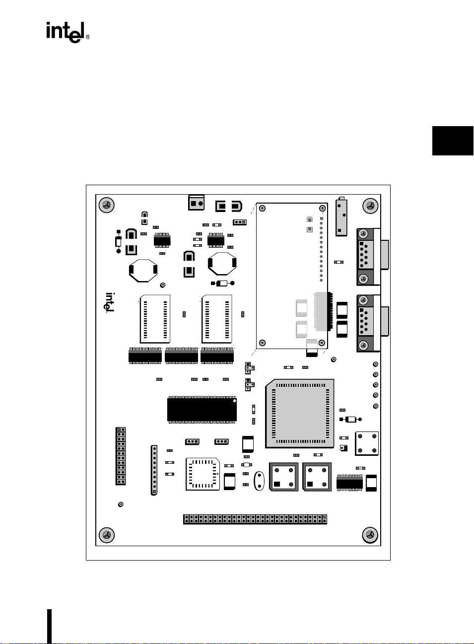
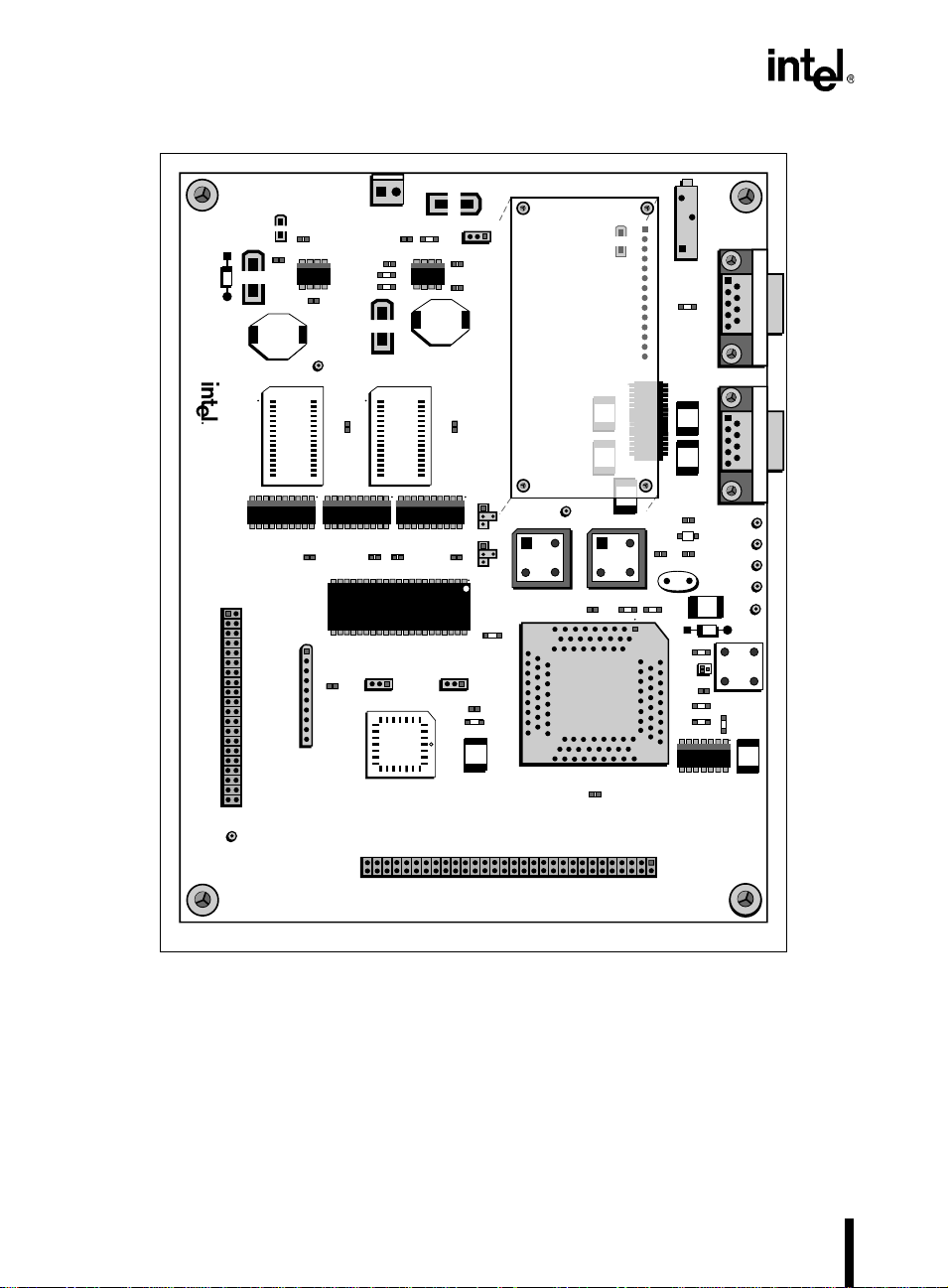
This chapter des cribes t he Intel 18 6 EC/EB Eval uation Boar d kit, and provi des se tup instru ctions.
Figure 2-1 shows the 80x186 EB Evaluation Board layout, and Figure 2-2 shows the EC board
layout. Refer to these figu res wh en you are fo llow ing the inst ructio ns in this ch apt er for se tting
up your evaluation board.
J1
R2
P1
R3
P2
C2 C3
DCE ConnectorPC Interface
TP6
GND
R5
V
CC
JP1
V
CC
TP1
TP4 TP3 TP2
TP5
C4
D1
R4
Q1
S1
R1
C1U1
C32
C33
GND
JP2
L3
TP8
C31
U14
V
CC
T0INT1OUT
T1INT0OUT
GNDGND
INT0P2.2
INT1P2.3
INT2BCLK0
INT3P2.6
INT4P2.7
GNDGND
GCS6#+5V
GCS7#+12V
D3
80X186EB EVAL 3V / 5V
V
CC
RP1
GND
C34
C26
TP7
C30
R12
R13
C28
U11
U13
J2
+5V GND
C25
R10
R11
C27
C29
U12
186/188
SELECT
GNDGND
C24
CLKOUTDT-R#
+5VDEN#
C22 R9
C23
E3
ABC
GCS5#BHE#
+12VRESOUT
PWRDN
NMIWR#
LOCK#RD#
U6
C14
FLASH
U10
ALELA19
5V/3V Select
CBA
C20
U7
C21
L2
D2
U8
U9
E4
ABC
R8
C19
READYLA18
HOLDLA17
HLDALA16
GNDGND
C12
E1
C13
PROT
WRT
A B C
A B C
SELECT
C15
C17
C18
AD15LA15
AD14LA14
C5
U2
C8C7
C6
E2 D
E3
U4
D
V
PP
C11R7
C16
L1
U5
Y1
AD13LA13
AD12LA12
AD11LA11
AD10LA10
AD9LA9
AD8LA8
C9
R6
C10
U3
GNDGND
AD7LA7
AD6LA6
AD5LA5
AD4LA4
AD3LA3
AD2LA2
AD1LA1
AD0LA0
2
Figure 2-1. Intel 186 EB Evaluation Board Layout
A5289-01
2-1
Page 18
INTEL 186 EB/EC EVALUATION BOARD USER’S MANUAL
C32
C33
D3
80X186EC EVAL 3V / 5V
C31
L3
GND
C30
C26
TP7
U13
U11
C27
J2
+5V GND
C24
R12
R13
C21 R11
C25
5V/3V Select
U6
U7
C15
CBA
C20
C22
C19
E1
L2
WRT PROT V
C12C11
J1
R2
C8
U2
R3
C2 C3
P1
P2
DCE ConntectorPC Interface
E2 D
A B C
C34
RP1
U12 U8
186/188
SELECT
C29
GNDGND
CLKOUTDT-R#
C23C28
ABC
+5VDEN#
+12VRESOUT
E5
GCS5#BHE#
NMIWR#
LOCK#RD#
ALELA19
U14
JP2
T1OUTT0IN
T0OUTT1IN
V
V
CC
CC
P3.0INT0
P3.1INT1
P3.2INT2
P3.3INT3
P3.4INT4
P3.5INT5
WDTOUT#INT6
GNDINT7
BCLK0INTA#
P2.3GND
RXD1DRQ0
TXD1DRQ1
P2.6DRQ2
CTS1#DRQ3
GNDGND
+5VGCS6#
+12VGCS7#
GND
TP8
C16
FLASH
PWRDN
U10
READYLA18
HOLDLA17
U9
ABC
C18
HLDALA16
A B C
PP
SELECT
E4
GNDGND
AD15LA15
R9
C17
R10
E3
D
AD14LA14
AD13LA13
AD12LA12
U5
AD11LA11
AD10LA10
AD9LA9
GND
AD8LA8
GNDGND
AD7LA7
TP6
U3
AD6LA6
C14
AD5LA5
AD4LA4
C10
AD3LA3
AD2LA2
AD1LA1
AD0LA0
TP1
C4
L1
C9
C5
TP4 TP3 TP2
Y1
TP5
R7R8C13
U4
V
CC
JP1
V
CC
C6
D1
R4
Q1
C7
R5
R6
S1
R1
C1U1
A5288-01
Figure 2-2. Intel 186 EC Evaluation Board Layout
2-2
Page 19

GETTING STARTED
2.1 SYSTEM REQUIREMENTS
• IBM* PC AT, XT or BIOS-compatible computer host system (interfaces via COM1 or
COM2 at 9600 baud).
• 5 V power supply (the connector housing and contact pins are included in the kit).
2.2 WHAT’S IN YOUR KIT
Evaluation Board Your kit includes a board with either a 3.3 volt, 16 MHz
80L186EB or 80L186EC microprocessor installed. Separately
packaged components included with the board are 5 VDC versions of the microprocessor and SRAM for conversion to a
5 VDC evaluation platform.
Monitor Program The Embedded Controller Monitor (ECM) program supports
basic software and hardware evaluation and basic debug facilities
(LOAD, GO, STEP, etc.) on the evaluation board. The ECM consists of two prog rams : RISM -186 ex ecutes in the ev aluat ion boa rd
and ECM-86 executes in an IBM PC or BIOS-compatible computer, called the host PC. These two programs communicate
through an asynchronous serial channel using a binary protocol
defined specifically for this application.
The source co de for the monitor soft ware is pro vid ed on a di sket te
included in your kit; this allows you to update the software for
various operating conditions in your target application.
Contents on Disk In addition to Flash downloading software, a diskette provided in
the kit contains schematics, a pld file for the programmable logic
device used on the board, and a sample assembly file for working
the with L CD display. Compiler software is not included in the
kit.
2
Software Development
Kit
Flash Loading
Utility
Serial Cable A serial cable is provided to connect the evaluation board to the
The kit provides a software development kit, which includes a
software debugger, locator, and sample code.
Users can download application programs to the on-board Flash
memory for execution. The Flash loading uti l it y is co nta in ed on a
diskette, and a separate manual, the CQI Flash Loader User’s
Manual, provides instructions for using this utility.
host PC.
2-3
Page 20

INTEL 186 EB/EC EVALUATION BOARD USER’S MANUAL
2.3 VIEWING THE BOARD SCHEMATICS
The schematics provided on the diskette are in the Adobe* Acrobat .pdf format. You can view
and print the schem atic s using the Acrobat Reader. The Reade r is availa bl e at no char ge from the
Intel World Wide Web site (http://www.intel.com/) or from the Adobe site
(http://www.adobe.com/).
2.4 SETTING UP THE EVALUATION BOARD AND THE HOST PC
This section tells you how to set up the board for use with a host PC. This section assumes you
won’t be using some of the advanced features of the board when you first power it up. For
additional options, such as selecting 80188 evaluation mode, refer to Chapter 3, “Hardware
Overview.”
1. Make sure you are in a static-free environment before removing any components from
their anti-static packaging. The evaluation board is susceptible to electro-static discharge
damage; such damage may cause product failure or unpredictable operation.
2. Inspect the contents of your kit. Make sure that all items are included. Check for damage
that may have oc cur re d during shipmen t. Cont act y our sales repres ent at iv e i f any items are
missing or damaged.
CAUTION: Many of the connectors on the evaluation board provide power through non-
standard pins. Connecting the wrong cable or reversing the cable can damage the
evaluation board and may damage the device being connected. Use extreme
caution when preparing to connect cables to this product.
3. Connect the power supply. The Intel 186 EC/EB Evaluation Board operates from a
5 VDC ± 10% power supply plugged into the J2 power connector (see Figures 2-1
and 2-2). This 5 volt signal is stepped down to 3.3 volts on the board. The connector
housing and contact pins provided in your kit match the power supply to the J2 connector.
To select 5 V, place a jumper on pins B and C of jumpe r E1. To select 3 V, place a jumper
on pins A and B of jumper E1. See Figures 2-1 and 2-2 for jumper locations.
All devices on the board operate at both 3.3 volts and 5.0 volts (except the LCD display,
which is hardwired to 5 volts). This option allows comparison of current consumption
when running code at either voltage. Separately packaged 5 V versions of the 80C186
processor and SRAM must be installed on the board for 5V operation.
2-4
Page 21

GETTING STARTED
4. Apply power to the host PC and the evaluation board.
When power is applied to the board, the message “i186 Ex 3V/5V EV” should appear
across the LCD display. This message indicates board initialization is complete. If the
message does not appear, press the reset button (S1).
Connect one end of the standard 9-pin AT-type serial connector to header P1 on the
evaluation board. Connect the other end to the COM1 port of the host computer. (You can
use COM2 if you need to, but you’ll have to specify COM2 when you run the Monitor
Software.) The PC and board communicate at 9600 baud.
After connection to the PC, the processor may appear to be held in the reset state. The
reason this occurs is that one of the host signals is used to reset the board. This signal may
be active prior to invoking the ECM86 host software on the PC. The PC and board
communicate at 9600 baud.
5. Insert the ECM-86 floppy disk provided with your kit in the floppy drive on the host PC.
You can run the ECM86 program directly from the diskette or copy the contents of the
diskette to your hard drive.
6. At the DOS prompt, change to the floppy disk drive (or to the directory to which you
copied the files in the previous step) and enter this command:
ECM86
After a moment, the PC should display the ECM86 monitor screen.
Comple te information on using the monitor software is located in Chapters 4 and 5.
2
2-5
Page 22

Page 23

Hardware Overview
3
Page 24

Page 25

HARDWARE OVERVIEW
CHAPTER 3
HARDWARE OVERVIEW
The evaluation board comes with a 16 MHz 80L186 EB or EC processor, 512 Kbytes of Flash
(containing the iRISM-186 monitor and a Flas h loa der utility in the boot blo ck) , and 256Kbytes
of SRAM. The expansion connector (JP1) supports up to 1 Mbyte of external memory and
64 K bytes of external I/O. Refer to Figures 2-1 and 2-2 for the exact locations of connectors,
jumpers and headers listed in this chapter.
The board utilizes the high peripheral integration of the 186 product family. The programmable
chip-selects support on-board memory, expansion memory, and the LCD interface. The
timer/counter unit controls timing for LCD display accesses. The serial control unit communicates with the hos t PC throug h the i ECM-86 softwa re and the Fl ash lo ader host softwa re. Fin ally,
the I/O port unit controls on-board power management functions (enable/disable serial drivers
and +12 volts).
Other on-chip peripherals are made available for hardware expansion via the JP1, JP2, and P2
connectors. The following sections describe in detail the specific devices used on the board.
3.1 JUMPER SUMMARY
Table 3-1. 80x186EB/EC Evaluation Board Jumper Settings
3
Jumper Name Description Options
E1 5 V/3 V Select Selects voltage (5 V or 3.3 V) that
E2 LA19/WRT PROT Selects options for Flash WP# pin.
E3 V
E4 Flash Powerdo wn
E5 186/ 188 Select Jumper for appropria te processor
†
Default setting
Select Selects 5 V or 12V programming
PP
Select
will be present on V
Includes option to make LA19
available t o Flash pi n 2 f or upg rading
to 8-MBIT component
(PA28F800BV).
voltage, as well as GND to remove
all program and erase capabilities.
Selects options for Flash RP# pin.
For normal operation, SW-RES# is
selected. To un l ock boot block
(regar dl e s s of WP#), 12 V is
selected.
type.
power plane.
CC
A-B = 3.3 V
B-C = 5 V
A-B = Write protect boot block
B-C = Unlock boot block
B-D = Add LA19 for 8- MBIT
Flash
A-B = Total WRT protect
B-C = 12 V program voltage
B-D = 5 V program voltage
A-B = Normal
B-C = Program boot block
override
A-B = 188 processor i nstalled
B-C = 186 processor in stalled
†
†
†
†
†
3-1
Page 26

INTEL 186 EB/EC EVALUATION BOARD USER’S MANUAL
3.2 MICROPROCESSOR
The core of the evaluation board is the 80x186 microprocessor. This processor operates at
3.3 volts up to 16 MHz in this board. Alternatively, the board can be configured to run at 5 volts
up to 33 MHz. To vary the CPU clock speed, an appropriate frequency value oscillator must be
installed at location U3 on the EC board and at location U5 on the EB board. The oscillator
operates at twice the frequency of the installed processor.
The 80x186 processor offers the following features:
• 16-bit data bus
• 1 Mbyte address space
• 2 on-chip UARTs
• 10 programmable chip-selects
• Interrupt control unit
• 3 programmable timer/counters
• Power management unit
• 32-bit watchdog timer (EC only)
• 4 DMA channels (EC only)
The 8-bit bus version of the processor (80C188/80L188) may also be used in this board. To
configure the board to operate with an 8-bit bus, jumper E5 must be in the A–B position. To
configure the board to operate with a 16-bit bus, jumper E5 must be in the B–C position. Many
of the proce ssor’ s on-c hip pe ripher als c an be a ccesse d usin g t he two e xpansi on conne cto rs on the
board (JP1 and JP2).
NOTE
Because host communications use the on-chip serial ports, changing the
operating frequency of the board requires the processor serial ports to be
reconfigured. The RISM monitor source code is provided on a floppy diskette
in your kit and is commented to indicate current register values.
3.2.1 Packaging
The 80x186 EC is packaged in a 100 lead PQFP and so cket and t he 80x186 EB is pac kaged in an
84 lead PLCC package and socket. Adaptors are available from Applied Microsystems Corp.*
and Emulation Technologies, Inc.* to allow for the connection of in-circuit emulators.
3-2
Page 27

HARDWARE OVERVIEW
3.3 MEMORY CONFIGURATION
The memory on the evaluation board can be divided into three types: Flash, SRAM, and
expansion. Flash memory contains the Flash loader utility, located in the boot block boundary,
and the RISM monitor program, beginning at F800:0000. Users can execute their test code from
boot-up using the Flash loader utility. Refer to the CQI Flash Loader Reference Manual for
instructions on programming the Flash memory. SRAM memory is used for the processor
interrupt vector table , stack all ocati on, and RISM da ta vari able s, and as a poss ible de st inati on for
user-writ ten code down loaded on the host i nterf ace. Expan sion me mory can be ac cessed through
the expansion interface, if required.
Table 3-2 shows the log ic al memory map and Figure 3-1 s hows the phys ic al memory ma p of t he
evaluation board.
Table 3-2. Logical Memory Map
Memory Area Start (H) Stop (H) Size
SRAM 0000:0000 2000:0000 128 Kbytes
Flash 8000:0000 F000:FFFF 512 Kbytes
Flash Boot Block FC00:0000 F000:FFFF 16 Kbytes
Expansion 4000:0000 8000:000 0 256 Kbytes
LCD (I/O) 0000:0400 0000:0440 64 bytes
3
3-3
Page 28

INTEL 186 EB/EC EVALUATION BOARD USER’S MANUAL
FFFFFH
UCS Flash
512 K
80000H
FFFFFH
Flash Loader Utility* (16K)
FC000H
Control Block
64 K
LCD Control
IO SpaceMemory Space
Peripheral
FFFFH
FF00H
0440H
0400H
Expansion
256 K
Unused
SRAM
128 K
Interru pt Vec t or Table at 00000H to 003FFH ( 1K)
LCS
LCS
GCS5
40000H
20000H
00000H
1Meg
UCS — Upper Chip Select
Start: 80000H Stop: FFFFF (Flash 512 K)
• 3 Wait Stat es
• Active for Memory Bus Cycles
• Bus Ready Not Required
LCS — Lower Chip Select
Start: 0000H Stop: 40000H (SRAM 128 K)
• 2 Wait Stat es
• Stop Address Required
• Active for Memory Bus Cycles
• Bus Ready Ignored
GCS5 — Expansion Memory
Start: 40000H Stop: 80000H (Expansion 256 K)
• Zero Wait Stat es
• Ignore Stop Address
• Active for Memory Bus Cycles
• Bus Ready Requi r ed
GCS7 — Expansion I/O
Start: 400H Stop: 500H
• Zero Wait States
• Ignore Stop Ad dress
• Active for I/O Bus Cycles
• Bus Ready Required
GCS2 — LCD Display I/O
Start: 400H Stop: 440H
• 8 Wait States
• Active for I/O Bus Cycles
• Bus Ready Ignored
* As shipped, RISM is located at F800:0000 and pointed to by the Flash lo ader utility during boot-up.
Figure 3-1. Physical Memory Map
3-4
Page 29

HARDWARE OVERVIEW
3.3.1 Flash (Program Memory)
Flash memory, as configured in the RISM monitor, is mapped to the upper 512 Kbytes of the
1 Mbyt e 80x186 proce ssor ad dress spac e. The board incl udes a singl e 4 Mbit, 32-pin PSOP Flash
device at locati on U9 with 110 ns access time at 3.3 V and 60 ns access time at 5 V. This memory
runs with one wait state at 5 volts/20 MHz and 3.3 volts/16 MHz.
The device data bus can be configured to be either 8 or 16 bits wide (corresponding to the
80x188and the 80x186 processor, respectively). Jumper E5 determines the Flash bus width.
When E5 is in the A–B position, the bus is 8 bits wide; when E5 is in the B–C position, the bus
is 16 bits wide. The configurable bus width allows access to all 512 Kbytes of Flash memory.
If a user app li cat i on r equi re s no nvolatile memory for storage, Flash can be erased and wr it te n by
jumpering E3 for either 5 V or 12 V programming voltage (V
) and using the proper
PP
programming algorithm. The SmartVoltage* Flash device can be programmed using either
voltage. The Flash loader utility is located in the Flash boot block (upper 16 Kbytes, FC000h to
FFFFFh). Writes to this region are prohibited, regardless of the voltage on V
, unless the RP#
PP
input is at +12 vo lt s or ju mp er E2 is s et to un lock the boot block . Jumpe r E4 controls the volt age
on RP#. When E4 i s i n the B–C position, the +1 2 vo lt s uppl y i s connected to RP#. When E4 is in
the A–B position, RP# is connected to the board reset signal.
CAUTION: To access boot block memory, E4 must be in the B–C position and Port Pin 1.1
must be programmed to a logic 0 (enabling +12 volts). Accessing the boot block is
not recommended, as the Flash loader utility code could be corrupted.
3
3.3.1.1 Setting Up the Board for Flash Downloading
You can use the Flash utility host program, FLASHLDR.EXE, provided in the kit to download
your application program to the Flash memory. Upon reset or power-up, the Flash loader reads
port pin to determine whether to execute a loaded program, such as RISM, or download new
software to Flash memory.
To set up the board for Flash downloading:
1. Power-off the evaluation board and disconnect the serial cable from the PC.
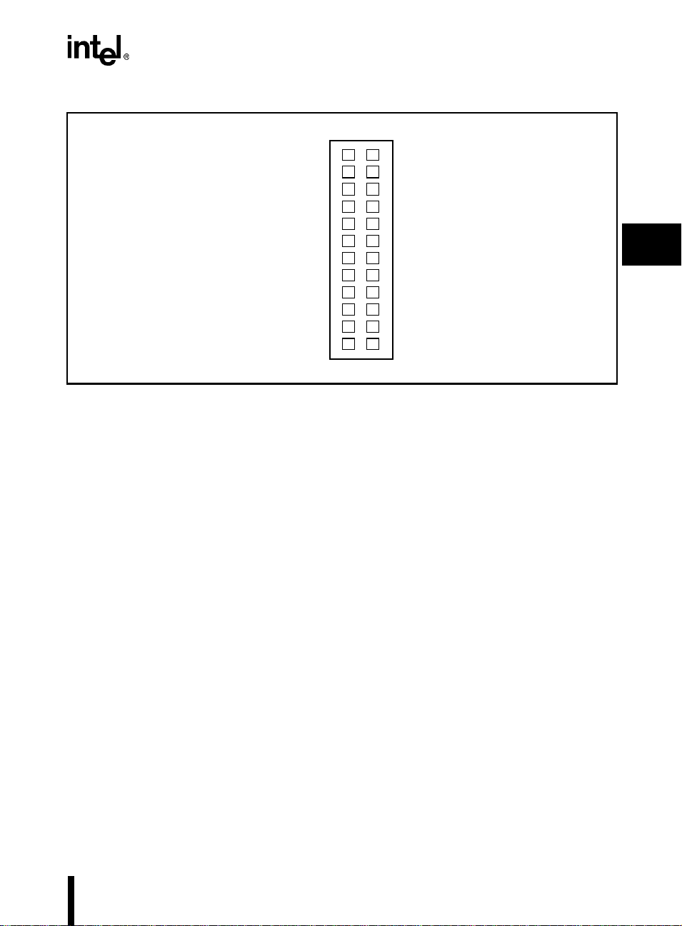
2. Port pin P2.6 on the secondary header (JP2) controls which programs execute at start-up.
Connect P2.6 to the +5 volt pin with jumper wire and 10 kΩ resistor. Figure 3-2 illustrates
this connection.
CAUTION: A 10 kΩ resistor is required when jumpering from the P2.6 pin to the 5 volt pin; if
this configuration is not used, the processor’s port control hardware could be
damaged.
3-5
Page 30

INTEL 186 EB/EC EVALUATION BOARD USER’S MANUAL
V
CC
Jumper Wire
10K ohm
P2.6
+5V
Jumper Wire
186 EB Connector JP2
V
CC
DRQ2
GCS6#
JP2
T1OUTT0IN
T0OUTT1IN
V
CC
P3.0INT0
P3.1INT1
P3.2INT2
P3.3INT3
P3.4INT4
P3.5INT5
WDTOUT#INT6
GNDINT7
BCLK0INTA#
P2.3GND
RXD1DRQ0
TXD1DRQ1
P2.6
CTS1#DRQ3
GNDGND
+5V
+12VGCS7#
186 EB Connecto r JP2 186 EC Connector JP2
186 EC Connector JP2
V
CC
T0INT1OUT
T1INT0OUT
GNDGND
INT0P2.2
INT1P2.3
INT2BCLK0
INT3
INT4P2.7
GNDGND
GCS6#
GCS7#+12V
Jumper Wire
10K ohm
Jumper Wire
A5420-01
Figure 3-2. Jumper Assembly for Flash Downloading
3. Reconnect the serial cable and power-up the board.
You should notice that the text CQFLASH LOADER now displays on the LED, signaling
that the board is ready for Flash downloading.
When the jumper assembly is installed, the Flash target program waits for commands from the
PC host, allowing you to use the provided Flash loader utility program to download programs to
the Flash.
3-6
Page 31

HARDWARE OVERVIEW
If this text does not display o n the LED, indicat ing a probl em with th e jumper as sembly, the board
boots as if no Flash loader assembly is installed; that is, the Flash target program immediately
starts the loaded user application program (for example, the iRISM monitor software).
You can find complete instructions for using the Flash utility program in the CQI Flash Lo ad er
User Manual included in your kit.
3.3.2 SRAM (Static Memory)
SRAM occupies the lower 128 Kbytes of memory starting at location 00000H. This memory is
used by the processor for interrupt vectors and stack allocation, by the RISM for program
variables, and by the user for downloaded code. The board includes two 1-Mbit, 32-pin SRAMs
with 17 ns access time at 3.3 volts. SRAMs are socketed to allow installation of 5 V SRAMs
(17 ns access time).
To allow insertion of both the 80x186 processor and the 80x188 processor, the memory is
configured such that only 128 Kbytes of the SRAM is accessible, even though 256 Kbytes of
SRAM are installed on the board.
3.4 PROGRAMMABLE LOGIC
All glue logic re quired by t he evaluatio n board is impl emented on a GAL 22 LV10C-15. The PLD
file located on the floppy diskette in your kit includes logic equations for this device. The logic
implemented inclu des the following:
• Inverting the Port Pin signal controlling V
(so VPP is disabled at reset)
PP
• Controlling the 8-bit/16-bit configuration for the Flash device
• Decoding the Enable signal for the LCD display
3
3-7
Page 32

INTEL 186 EB/EC EVALUATION BOARD USER’S MANUAL
3.5 POWER SUPPLY
The power supply connects to J2 on the board schematic. Pin 1 must connect to +5 volts and pin
2 must connect to g rou nd. The sup ply is then re gul ated to 3. 3 vol ts by t he on-b oard ci rc uitry. The
V
for the board is controlled by jumper E1. When E1 is in the A–B position, VCC = 3.3 volts;
CC
when E1 is in the B–C position, V
= 5.0 volts. VCC is converted t o +12 v olts f or opt ional Flash
CC
programming voltage.
E1
A
B
C
A – B
B – C
VCC = 3.3 volts
VCC = 5.0 volts
A2607-01
Figure 3-3. E1 Jumper
The LCD display controller VCC pin connects directly to the 5 volt supply, not the VCC plane,
allowing 5 volt operation only.
21
+5VDC - V
Ground - V
CC
SS
Figure 3-4. J2 Power Connector
The Maxim* MAX750 component at U6 (EC) or U7 (EB) is a current-mode DC-DC converter.
This device takes the 5 volt supply and steps it down to 3.3 volts. This voltage output is always
supplied to provide V
for the processor, memory, and logic when selected at E1.
CC
3-8
Page 33

HARDWARE OVERVIEW
The Maxim MAX734 loc at ed at U11 is al so a cur rent-mode DC-DC conv er ter . T his device steps
up the V
voltage to +12.0 volts. This voltage output is supplied to provide a VPP option for
CC
Flash memory programming. The SHDN# input (pin 1) connects to a port pin (P1.1) on the
processor through an inverter. At reset, SHDN# is driven low to disable the +12 volt signal. The
output remains disabled until Port Pin 1.1 is programmed to a logic 0. When SHDN# is low, the
output (pin 8) is V
minus a diode drop. The evaluation board uses SmartVoltage Flash. To
CC
prevent unintentional writes to Flash, set jumpers E2 and E3 as indicated in Table 3-1.
3.6 SERIAL INTERFACE
Connector P1 c onne ct s t o yo ur PC’s serial por t. P1 i nt erf aces pin-to-p in wit h a st andard nine-pin
RS-232 serial connector. Verify that the cable being used provides all signals required.
Table 3-3. P1 Host Serial Connector
P1 Connector
1234 5
6
78
9
Pin
Nos.
1 (CF) DCD Data Carrier Detect DTR P1-pin 4
2 (BB) RxD Receive Data TxD of MAX561
3 (BA) TxD Transmit Data RxD of MAX561
4 (CD) DTR Data Terminal Ready INIT
5 (AB) SG Signal Ground Digital Ground
6 (CC) DSR Data Set Ready DTR P1-pin4
7 (CA) RTS Request To Send CTS P1-pin8
8 (CB) CTS Clear To Send RTS P1-pin7
9 (CE) RI Ring Indicator Run Indicator
Host RS-232
Signal Name
Connection on
Evaluation Board
Connector P2 is an additional serial port for user applications. Receive, Transmit, and Clear-toSend are connected. Other connector pins are routed to test points on the board.
3
3-9
Page 34

INTEL 186 EB/EC EVALUATION BOARD USER’S MANUAL
Table 3-4. P2 Serial Channel 0
P2 Connector
1234 5
6
78
9
Pin
Nos.
1 (CF) DCD Data Carrier Detect Test Point 1
2 (BB) RxD Receive Data RxD
3 (BA) TxD Transmit Data TxD
4 (CD) DTR Data Terminal Ready Test Point 4
5 (AB) SG Si gnal Ground Digital Ground
6 (AB) DSR Data Set Ready Test Point 2
7 (CD) RTS Request To Send Test Point 3
8 (BA) CTS Clear To Send CTS
9 (BB) RI R ing Indicator Test Point 5
Host RS-232
Signal Name
Connection on
Eval uation Board
The two serial connectors are connected to the Maxim MAX561, an EIA/TIA-562
Driver/Rece iver. Th is devi ce ope rates from a 3.3 volt V
(or 5 volts, o pti onall y). The E IA/ TIA-
CC
562 standard is a low voltage serial communications protocol. This protocol operates at ±3.7
volts. The 3.3 volt signals from the board are charge-pumped to ±6.6 volt levels internally,
conforming t o t hi s s ta ndard. Signals from the seria l conn ect or s, P 1 and P2, are tr ans la te d t o a 3.3
volt level. Output from this device is recognized by EIA/TIA-232-D receivers, and inputs can
handle EIA/TIA-232-D levels without damaging the device. The MAX561 SHDN pin (pin 25)
connects to port pin 1.0 on the 80x186 processor. When this pin is programmed to a logic 1, the
Maxim device will go into shutdown mode, reducing current consumption to leakage. During
initialization, port pin 1.0 is programmed t o a l ogi c 0 to enable communi ca ti on wi th the host PC.
Serial communications on the evaluation board are controlled by the 80x186 processor on-chip
serial ports. Serial Port 0 on the microprocessor handles PC communications via connector P1.
Serial Port 1 is available for user applications via connector P2. The 80x186 processor supports
synchronous serial communications as well as various modes of asynchronous communications.
The time base for the host interface is a 6.0 MHz oscillator connected to BCLK0, the external
serial clock i nput on the 80 x186 process or. This al lows the use r to change t he process or oper ating
frequency without altering the baud rate.
NOTE
The BCLK0 input must be less than half the processor operating frequency
(which is half the clock input frequency). Operating the processor below
12.288 MHz requires reprogramming the serial control unit on the 80x186
processor. The source code for the RISM monitor is provided on a floppy
diskette included in your kit for this purpose.
Figure 3-5 on page 3-11 illustrates the adaptor cable needed if your PC has a 25-pin serial port
connector.
3-10
Page 35

To Evaluation Board
DCD
1
DSR
6
RXD
2
RTS
7
TXD
3
CTS
8
DTR
4
RI
9
GND
5
P1
Note:
Signal mnemonics are referenced to the host.
HARDWARE OVERVIEW
To Host PC
Shield Ground
TXD
RXD
RTS
CTS
DSR
GND
DTR
DCD
1
14
2
15
3
16
4
17
5
18
6
19
7
20
8
21
9
22
RI
10
23
11
24
12
25
13
3
Figure 3-5. 25-Pin to 9-Pin Adaptor
A2343-02
3-11
Page 36

INTEL 186 EB/EC EVALUATION BOARD USER’S MANUAL
3.7 EXPANSION INTERFACE
There are two expansi on conne ctors on the evalua tion b oard. Ref er to the schemat ics in clude d on
a floppy diskett e in your ki t for repr esentat ion of the co nnector pi nouts. The 60- pin JP1 conn ector
(Figure 3-7) provides latched address pins and the address/data bus signals. This connector also
provides access to all bus-control signals, programmable chip-selects, +3.3 volts, +5 volts, and
+12 volts. The JP2 connector provides access to on-chip peripherals of the 80x186 processor.
This connector allows access to interrupt inputs, timer inputs and outputs, port pins, CLKOUT,
RESOUT, +3.3 volts, +5 volts, and +12 volts. The JP2 connector contains 40 pins for the EC
processors (see Figure 3-6) and 24 pins for the EB processors (see Figure 3-7).
NOTE
3.3 volts is available on the connector only when jumper E1 selects VCC = 3.3
volts; otherwise, these pins are 5 volts. +12 volts is available on the connector
only when Port Pin 1.1 is programmed to a logic 0; otherwise, these pins are
V
minus a diode drop.
CC
..............................
V
SS
T1IN.............................
V
..............................
CC
INT0.............................
INT1.............................
INT2.............................
INT3.............................
INT4.............................
INT5.............................
INT6.............................
INT7.............................
INTA#...........................
V
...............................
SS
DRQ0...........................
DRQ1...........................
DRQ2...........................
DRQ3...........................
V
...............................
SS
GCS6#..........................
GCS7#..........................
1
3
5
7
9
11
13
15
17
19
21
23
25
27
29
31
33
35
37
39
2 - T1OUT
4 - T0OUT
6 - V
CC
8 - P3.0
10 - P3.1
12 - P3.2
14 - P3.3
16 - P3.4
18 - P3.5
20 - WDTOUT#
22 - V
SS
24 - BCLK0
26 - P2.3
28 - RXD1
30 - TXD1
32 - P2.6
34 - CTS1#
36 - V
SS
38 - +5VDC
40 - +12VDC
Figure 3-6. 186 EC Peripheral Expansion Connector JP2 (40 pin)
3-12
Page 37
HARDWARE OVERVIEW
............
V
CC
T1OUT.......
T0OUT.......
V
.............
SS
P2.2............
P2.3............
BCLK0........
P2.6............
P2.7............
V
.............
SS
+5V.............
+12V...........
1
3
5
7
9
11
13
15
17
19
21
23
2 - V
CC
4 - T0IN
6 - T1IN
8 - V
SS
10 - INT0
12 - INT1
14 - INT2
16 - INT3
18 - INT4
20 - V
SS
22 - GCS6#
24 - GCS7#
Figure 3-7. 186 EB Peripheral Expansion Connector JP2 (24 pin)
3
3-13
Page 38

INTEL 186 EB/EC EVALUATION BOARD USER’S MANUAL
JP1 Memory - I/O Expansion Connector
2x30 Pin Molex* 39-51-6004 or Equivalent
..............................
V
CC
LA0 Output..................
LA1 Output..................
LA2 Output..................
LA3 Output..................
LA4 Output..................
LA5 Output..................
LA6 Output..................
LA7 Output..................
V
..............................
SS
LA8 Output..................
LA9 Output.................
LA10 Output................
LA11 Output................
LA12 Output................
LA13 Output................
LA14 Output................
LA15 Output................
V
...............................
SS
LA16.............................
LA17............................
LA18...........................
LA19...........................
RD#............................
WR#............................
BHE#..........................
RESOUT.....................
DEN#...........................
DT-R#.........................
V
..............................
SS
1
3
5
7
9
11
13
15
17
19
21
23
25
27
29
31
33
35
37
39
41
43
45
47
49
51
53
55
57
59
2 - V
CC
4 - D0 Bidirectional
6 - D1 Bidirectional
8 - D2 Bidirectional
10 - D3 Bidirectional
12 - D4 Bidirectional
14 - D5 Bidirectional
16 - D6 Bidirectional
18 - D7 Bidirectional
20 - V
SS
22 - D8 Bidirectional
24 - D9 Bidirectional
26 - D10 Bidirectional
28 - D11 Bidirectional
30 - D12 Bidirectional
32 - D13 Bidirectional
34 - D14 Bidirectional
36 - D15 Bidirectional
38 - V
SS
40 - HLDA
42 - HOLD
44 - READY Input
46 - ALE
48 - LOCK#
50 - NMI
52 - GCS5#
54 - +12 VDC
56 - +5 VDC
58 - CLKOUT
60 - V
SS
3-14
Figure 3-8. CPU Bus Expansion (EB and EC)
Page 39

HARDWARE OVERVIEW
3.8 LCD INTERFACE
The evaluation board includes a 16-character by 1-line LCD display. The display has an 8-bit
interface and is de signed to o perat e at up to 20MHz. The displa y inc lud es a Hitach i* 447 80 LCD
display cont roll er th at tak es car e of funct ions s uch as char acte r inte rp retat ion an d displ ay ref resh.
The display i s write-only. T his i s b eca use the displ ay cont ro ll er operates a t 5 v olt s V
part driving a 3.3-volt bus can damage parts operating at 3.3 volts V
. This means that the
CC
. A 5-volt
CC
BUSY pin of the processor can not be monitored to det er mine when the pr oc essor is rea dy for t he
next command, so a delay loop must be used to allow the display to finish commands.
Signals from the 80x186 processor can be connected directly to the LCD controller inputs,
regardless of V
, because 3.3 volt and 5 volt outputs are compatible with 5 volt TTL level
CC
inputs.
The LCD display is mapped in I/O space at 400H to 440H. All command and data writes to the
display are t o this addre ss. Port pin 1.4 is used to c ontrol whi ch LCD regis ter is acc essed. P1.4= 0
accesses the command register; P1.4 = 1 accesses the data register.
3.8.1 LCD Interface Demo
The diskette provided in your kit includes a file, LCD_DEMO.ASM, that contains source code
you can assemble and load onto the board (using iECM). You can execute the program for a
demonstration of the basic principals of operating the LCD display module. This program prints
a static message to the display. The source code is commented to serve as a tutorial and can be
adapted as needed for other applications and messages. Note that although the LCD module is
capable of displaying standard ASCII (characters 32 through 125) or custom characters, this
demo uses only ASCII characters.
For more infor mat ion re gardin g t he opera tion o f the d is play co ntrol le r, ple ase re fer to th e Hitac hi
LCD Controller/Driver LSI Data Book.
3
3-15
Page 40

Page 41

Introduction to the
Software
4
Page 42

Page 43

CHAPTER 4
INTRODUCTION TO THE SOFTWARE
The Intel 186 EC/ EB Eva luation Board us es an Embedd ed Contr oller M onitor ( ECM) wr itte n for
the 80x186 family of 16-bit microprocessors. This monitor supports basic debug facilities
(LOAD, GO, STEP, etc.) in the user’s target system. The ECM is broken into two independent
programs. One of these (iRISM-186) executes in the evaluation board and the other (iECM-86)
executes in an IBM PC or BIOS-compatibl e c om put er . These two programs communicate via an
asynchronous serial channel using a binary protocol defined specifically for this application.
The partitioning of the ECM into two separate programs supports a number of goals:
• The system is easy to adapt to a new target because the code that runs in the target is very
simple and small.
• The feature set of the user interface is not limited by the resources of the target, since the
user interfa ce is impl em ent ed in the host PC .
• Concurrent operation of the ECM and the target system is easily achieved. This allows you
to interrogate and (carefully) modify the state of the target system while it is running.
This chapter descri bes the us er inter face provided b y the i ECM-86, the interf ace betw een this PCresident software and the target-resident software, and the structure of the software in the target.
The board uses the internal 80x186 EB/EC serial port for host communications.
4
The iECM-86 software was created by Intel to support users of the 80x186 architecture and is
placed in the public domain with no restrictions or warranties of any kind.
4.1 SOFTWARE FEATURES
The iECM-86 software has the following features:
• Sixteen software execution breakpoints
• Concurrent interrogation of target memory and registers
• Supports BYTE, CHARACTER, WORD, STRING, DOUBLE WORD, and REAL variable
types
• Supports LOAD, SAVE, LIST, LOG, and command INCLUDE files
4-1
Page 44

INTEL 186 EB/EC EVALUATION BOARD USER’S MANUAL
4.2 RESTRICTIONS
Two words of the user stack are reserved for use by the iRISM-186 software. Other memory
and/or regi ster s in th e targ et me mory are use d by the iRI SM-186 softwa re. The exac t amo unt and
location of this memory is implementation-dependent.
An asynchronous serial port capable of operation at 9600 baud must be available in the target
system. The RISM described in this document uses the 80x186 EB/EC internal serial port.
The TRAP instruction is reserved.
Breakpoints and program stepping will not operate if the user’s code is in Flash or other
nonchangeable memory.
4.3 EMBEDDED CONTROLLER MONITOR (ECM)
An ECM (Embedded Controller Mon itor) is installe d in your target system to pr ovide basic debug
capability. Capabilities include lo ading object files into system RAM, examin ing and modifying
variables, executing code, and stepping through code. A personal computer acts as the host for
program translation and emulates a video display during user interaction with the ECM. The
ECM developed f or the 80x186 famil y makes the assumpt i on t ha t t he user interface is a person al
computer; no provision is made for interface to a CRT terminal. By making this assumption, it is
possible to re duc e t h e s iz e an d com p lexity of the c ode t hat must be inst alled in the t arget system.
The term coined for this target-resident code is Reduced Instruction Set Monitor (RISM).
The RISM consists of about 2200 bytes of 80x186 code that provides primitive operations.
Software running in the host uses the RISM commands to provide a complete user interface to
the target system. The advantage of this approach is that the ECM can be readily adapted to
different tar g et sys tems and requires only a sma ll par t of t he available targ et mem or y space. The
disadvantage is that the user interface must be provided by a personal computer.
RISM is structured as a short section of initialization code and an interrupt service routine (ISR).
The ISR processes interrupts from the host system. The RISM ISR consists of a short prologue
and a case-jump to one of 20 to 25 command executors. These executors are simple and short;
the flow though the e nti re ISR (i nc luding the prologue) is 15-20 instructi ons. The serial communication occu rs at 96 00 baud, which li mits the frequenc y of the se inter rupts t o 1 KHz. In the worst
case, the board will be slowed by the execution of a fairly short RISM ISR every millisecond
while executing user code. It is possible to operate the board so that no real time is lost to the
iECM-86 unless the user is actively interrogating the target. See “Initiating and Terminating
iECM-86” on page 4-3 and the description of the RISM REPORT_STATUS code (Code 14H)
on page 6-5 for details.
4-2
Page 45

INTRODUCTION TO THE SOFTWARE
4.4 USER INTERFACE
The user interface to the iECM-86 supports commands to initiate and configure the ECM-86,
perform I/O operations involving DOS files, execute user programs, and interrogate variables in
the target sy stem. Inter rogation can be done in a numb er of format s and in most case s can be done
concurrently with user code execution.
4.4.1 Numeric Input
The command parser used by the iECM-86 software requires that numeric inputs always start
with the digits 0-9. Hexadecimal numbers that start with A–F must be preceded by a zero. For
example, enter “0AA55” instead of “AA55.” This requirement is similar to that of ASM86.
4.4.2 Controlling Lengthy Commands
Most of the commands supported by iECM-86 appear to complete without delay. Some
commands (f or exa m ple , d isp laying or fil l ing a large area of memory) t ake an appreciable l en g th
of time to complete. In general, these commands can be aborted by pressing Enter. Those
commands that display a large amount of information can be paused by pressing the spacebar.
After you have checked the data on the screen, you can press the spacebar again to resume the
output.
4
4.4.3 Aborting from iECM-86
Press Ctrl+C to close any open files and return to DOS.
4.5 INITIATING AND TERMINATING iECM-86
This section descri bes t he command s for invoki ng iECM -86 f rom DOS and exit ing ba ck to DOS.
4.5.1 ECM86
This command, entered at t he D OS p rom pt , l oads the iECM-86 software and e xecutes it. Se ver al
options are available with this command. Option strings always start with a hyphen (-) and can
be entered in upper or lower case. The operation of these options is described below. Any or all
of these options can be entered in any order. If the options are contradictory, the actual option
accepted is the last one entered.
4-3
Page 46

INTEL 186 EB/EC EVALUATION BOARD USER’S MANUAL
4.5.2 -COM2, -COM1
These options tell the iECM -86 softwa re which ser ial communic ation port is to be use d. If neith er
option is entered, COM1 is used as a default. If iECM-86 detects valid CTS (Clear to Send) and
DSR (Data Set Ready) signals from the appropriate COM port, it signs on and displays a
command prompt. When the target is stopped, the command prompt is an asterisk (*). When the
target is already running, the prompt is a greater-than sign (>).
4.5.3 -DIAG
If CTS and DSR are not present, iECM-86 displays a warning message. You can choose to
proceed or exit. It is possible, but not likely, that iECM-86 will operate properly even after the
warning. It is more likely that ther e is a prob lem with the serial port or th e cabling that preve nts
proper operation.
If the problem is not obvious, such as a disconnected cable or no power to the target hardware,
use the -DIAG invocation option to help isolate the problem. The -DIAG option puts the iECM86 system in a special mode that allows many tests to be used to find interfacing problems or
target bugs.
The diagnostic mode is intended to support debugging of boards that use iECM-86 software. It
also provides a simple routine to check the communications interface between the host and the
target.
In the board , a seri al por t loo p-back mo de all ows de buggin g the ho st/bo ard inter face. Upon res et,
the board is in the echo mode. Until it receives an ASCII slash (/) or backslash (\), it increments
every character it receives from the host and sends the incremented value back to the host. The
LCD dis plays the word “DIAGNOSTICS” when the board is in echo mode. If a backslash is
received by the RISM, the board leaves echo mode and starts normal operation. When a slash is
received, the board stops echoing incremented received data and starts responding to RISM
commands with the diagnostic flag set.
NOTE
The target hardware has to be reset before using the -DIAG option. When
executing diagnostic routines from Flash, certain commands such as
breakpoints and stepping will not work because they need to modify the code
to work properly.
When the host software is invoked in the diagnostic mode, it prompts you to enter characters on
the keyboard. Thes e charac ters are sen t to the target , and the res ponse from the ta rget i s displayed
on screen. This is a simple confidence check on the serial communication channel. You are told
to enter a slash or backslash to terminate this mode and proceed in either the diagnostic mode or
the normal user’s mode. If the user interface is invoked without the -DIAG option, the software
immediately transmits a reverse-slash, which should put the target in the normal mode.
4-4
Page 47

INTRODUCTION TO THE SOFTWARE
4.5.4 -POLL, -SIGNAL
These two options contr ol how the host software detects whether or not the user’s code is running.
If poll mode is selected, the host periodically polls the target with a REPORT_STATUS
command. This takes no additional hardware, but it forces the target to spend instruction cycles
responding t o the p oll. The si gnal m ode av oids t hi s overh ead, but it requi res t hat t he tar get se t t he
Ring Indicator modem line before it issues a REPORT_STATUS command. If neither option is
selected, the s ig nal mo de i s s elect ed as a default. On the boar d, t he P1.3 pin of 80x186 p roc ess or
is used to generate this running signal. Therefore, the signal mode is recommended. (The
REPORT_STATUS command is described on page 6-5.)
4.5.5 RESET SYSTEM, RES SYSTEM, RESET, RES
This command and its abbreviations reset the entire target hardware system. This command
operates by dropping the DTR modem control line. This comes into the target as DSR. After
dropping DTR, the iECM-86 software waits about 1 second to allow the target to complete its
initiali zation r outines. The iECM -86 warns of this time dela y and th en ignores input fr om the ho st
PC until it e xpi res. Unless spe ci al pr ecautions are taken in the design of a ta rge t system, any da ta
in RAM (including downloaded object code) may be corrupted by the reset. On the board, the
RAM contents should not be affected by a reset.
4
4.5.6 DOS
This command enables you to temporarily leave iECM-86 and return to DOS. Once you have
suspended iECM-86, you may perform other functions in DOS, including using other software
programs such as ASM86, as long as there is sufficient memory to do so.
To re-enter i ECM-86, type exi t at the DOS prompt. i ECM-86 retur ns with all condi tions that were
in effect at the time it was suspended.
4.5.7 QUIT
This command closes any files that iECM-86 has opened and exits to DOS. Note that this
command can b e u sed eve n if the targ et is r unni ng. iECM -8 6 s ets the selec ted COM por t to 9600
baud, 8 bits, no parity and one stop bit. The port is left in this state by iECM-86 when control is
returned to DOS.
4-5
Page 48

INTEL 186 EB/EC EVALUATION BOARD USER’S MANUAL
4.6 RELATED INFORMATION
All unreser ved funct ions of the pr ocessor a re avail able to you, exc ept the Non-Maskab le In terrupt
(NMI), the Breakpoint instruction (INT 3), the Trap Flag (TF), 16 Kbytes of address space, and
128 bytes of I/O space.
4.6.1 Reserved Functions
The Trap Flag and its vector in memory locations 4H–7H are reserved for use by the SSTEP
command and BREAKPOINTS.
The NMI pin and its vector in memory locations 8H–0BH are reserved for use by the host
interface.
The INT 3 instruction and its vector in memory locations 0CH–0FH are reserved for use by the
SSTEP command and BREAKPOINTS.
4.6.2 Reserved Memory
On-board Flash memory, as shipped, is 32 Kbytes from address 0H to 7FFFH.
Addresses 0H–3FFH are the interrupt vectors for the processor.
You must not alter the interrupt vectors from 4H–0FH.
Memory locations 400 H–415H a re reserv ed for us e by the RI SM monitor c ode. You must ensu re
that no locations in this partition are used by code that is to operate with the RISM. The easiest
way of doing this is to generate an ASM-86 module that declares a DATA SEGMENT at 400H
that is 22 bytes long. This module can then be linked into the final program to prevent the linker
from assigning these registers to another module.
Fourteen words of user stack space must be reserved for use by the iRISM-186 software while
the board is processing a host interrupt. The CS:SP register pair is initialized by RISM to
0000H:0800H, providing a total stack size of 501 words before RISM data variables are
overwritten. If this is insufficient for your application, your code should alter the SP to a large
enough value. Normally, you should write your code to begin at address 800H and download it
to Flash memory using iECM-86. You should use any space left beneath your code as data
memory.
4.6.3 Reserved I/O
The I/O space from 400H–47FH is reserved for use by the host interface.
4-6
Page 49

iECM-86 Commands
5
Page 50

Page 51

This chapter defines the iECM-86 software commands.
5.1 ENTERING COMMANDS
The syntax for iECM commands is shown below:
COMMAND
metasymbol
CHAPTER 5
iECM-86 COMMANDS
iECM-86 command definitions use one or more of the following metasymbols:
addr
address iECM-86 is able to interpret the microprocessor’s address space as
either a flat 20-bit array or through segmentation. A location
anywhere within the 1 Mbyte memory range may be specified by its
complete physical address, such as 0F1AC9H.
segment:offset Memory may also be accessed by segments. Valid segment
references are the following (where segment and offset are valid
integers):
CS:offset
DS:offset
ES:offset
SS:offset
When using CS, DS, ES or SS, the full address i s c al cul at ed u si ng t he
actual value of the appropriate target processor segment register.
In addition to the above registers, iECM-86 maintains four userdefinable registers that may be used for segment variables:
CB:offset
DB:offset
EB:offset
SB:offset
5
This faci lity is useful w hen reading f rom assembler listings, wh ich
are typically offset from 0000. These base registers are used, for
example, as a base pointer to a block of memory for debug purposes.
CB could be loaded with the base address of a code module, then
breakpoints could be set using offsets from that base. Using these
internal iECM registers has no effect on the values of the target
processor's registers.
5-1
Page 52

INTEL 186 EB/EC EVALUATION BOARD USER’S MANUAL
bp_number Sixteen breakpoints are available to the user. This number selects
which breakpoint to access.
code_addr The code address may be specified by either segment: offset,
CS:offset, or CB:offset.
count This denotes the number of times a command executes.
filename This is the location (path) and name of the file you want to reference
(e.g., \progdir\program.obj).
value Data to be entered in the current base notation.
5.2 FILE OPERATIONS
iECM-86 uses f il es in the host sy st em to load and sav e o bject code, to ent er pr edef ined strings of
commands, to keep a log of commands that are entered by the user, and to keep a record of an
entire debug session that includes both the characters entered by the user and the responses
generated by i E CM-86 on the host s cr een. The commands th at operate with fi le s are descri bed in
the following sections.
5.2.1 Loading and Saving Object Code
iECM-86 accepts object files that are generated by Intel’s development tools. iECM-86 will not
accept file s that conta in unresolv ed external s or files that contai n re-locat able re cords. These files
must be passed through LINK86 and/or LOC86 to resolve the externals and/or absolutely locate
the re-locatable segments. iECM-86 will also not accept HEX format files. The iECM-86
commands that operate on object files are the following:
LOAD
filename
SAVE
addr
TO
addr
IN
filename
The metasymbol filename mean s t h at a va li d M S- DOS fi le na me mus t be entered in t ha t posi t ion
of the command string.
LOAD filename This command loads the content records of the object
file filename into the target memory.
SAVE addr TO addr IN filename This command saves a region of memory as an object
file that can be reloaded into the target memory at
some la ter time.
5-2
Page 53

iECM-86 COMMANDS
5.2.2 Other File Operations
In additio n to o bject file s, the i ECM-86 ma kes us e of i nclude fil es, lo g fil es, and l ist fil es. I nclude
files contain commands to be executed by iECM-86. They must contain the exact sequence of
ASCII characters that you would enter from the keyboard to execute the command. Include files
can be tedious to create with a text edito r, so iECM-86 ca n generat e log fi les tha t stor e charac ters
entered by the user. These log files may be used later as include files to recreate command
sequences. List files keep a running record of commands entered by the user and the responses
generated by iECM-86. Comments can be included in list and log files to make them easier to
understand. A comment starts with a semicolon (;) and ends with a carriage return or ESC. The
semicolon is co nsidered pa rt of the commen t, but the carriage ret urn or ESC is not. The command
parser ignores comments but puts them in the list and log files.
The list and l o g fi le commands allow for default f i le names a nd allow either overwriting existing
data in the fil e or appending data at the end of th e fi le . Thi s al lows you to gather li st a nd l og da ta
in the def ault file s, wh ich av oid s crea ting and managin g a large numb er of separ ate files. Log and
list files are stamped with the date and time whenever they are opened to facilitate using this
capability, then going back to sort out the data from several debug sessions with a text editor.
The following commands are used in include, log, and list operations.
INCLUDE
PAUSE
LIST
LIST
LOG
LOG
LISTOFF
LISTON
LOGOFF
LOGON
filename
filename
filename
Three of these commands requir e you to supply a valid f ile nam e; th e rest us e the app rop riat e file
name that has already been entered.
INCLUDE filename T his command attempts to open filename as a read-o nly file. If the
file can be opened, the command parser takes commands from that
file until the end of the file is reached. The INCLUDE file is then
closed. Only one INCLUDE file is opened at a time.
5
PAUSE This command is do cumented in th is sect ion beca use it is in tended t o
be used as part of INCLUDE files. It is not really a file-oriented
command itself. When this command is entered, the iECM-86 stops
5-3
Page 54

INTEL 186 EB/EC EVALUATION BOARD USER’S MANUAL
parsing commands until a space character is entered from the
keyboard (the space character can’t come from an INCLUDE file).
This allows the user to pause in the middle of an INCLUDE file
operation to see what is occurring and then acknowledge the pause
condition by pressing the space bar.
LIST This command behaves like the LIST filename command described
below, exce pt tha t it uses t he la st file name tha t wa s ente re d as par t of
a LIST filename command. If no such command has been entered,
the default filename LIST.ECM is used.
LIST filename This com mand attempts to open filename as a writable file. If
filename already exists, then iEC M -86 asks if the file is to be
overwritten or if the new d ata sho uld be appen ded t o the e xisti ng fi le.
It then opens the file and stamps it with the current date and time
from the system clock. Subsequent commands entered by the user
and the responses generated by iECM-86 are recorded in the file.
LOG This command behaves like the LOG filename command described
below, exce pt tha t it uses t he la st file name tha t wa s ente re d as par t of
a LOG filename command. If no such command has been entered,
the default file name LOG.ECM is used.
LOG filename This com mand attempts to open filename as a writable file. If
filename already exists, iECM-86 asks if the file is to be overwritten
or if the new data should be appended to the file. It then opens the
file and stamps it with the current date and time. Subsequent
commands entered by the user are recorded in the file. Note that this
file may contain nonprintable characters (e.g., ESC).
LISTOFF
LISTON The LISTOFF command closes a list file that has been specified by
the LIST command. This stops new list information from being
recorded. The LISTON command reopens the list file in the append
mode so that recording can start again. LISTON also stamps the list
file with the current date and time from the system clock.
LOGOFF
LOGON The LOGOFF command closes a log file that has been specified by
the LOG command. This stops new log information from being
recorded. The LOGON command reopens the log file in the append
mode so that recording can start again. LOGON also stamps the list
file with the current date and time from the system clock.
5-4
Page 55

iECM-86 COMMANDS
5.3 PROGRAM CONTROL
Commands that co ntr ol pr ogr am exe cut ion allow you to res et th e processor, set ex ecution breakpoints, start execution, stop execution, step, and super step. The commands are grouped by their
major functions for the sake of discussion.
5.3.1 Resetting the Target
The processor can be reset by executing the following iECM-86 command:
RESET CHIP
RES CHIP
This command physically resets the processor by setting the RISM_DATA register to
0XXXX0001 and issuing a MONITOR_ESC RISM command, which causes the target to
perform a JMP FFFF:0000H instruction.
RESET SYSTEM
RES SYSTEM
RES
This command resets the ent ire i ECM-86 sys tem, incl uding the tar get. It op erate s by bri nging t he
DCD line of the serial port low. This, with appropriate circuitry in the target system, resets the
target proces sor . Durin g this proce ss, the i ECM-86 sof tware mu st wait a bout one secon d to al low
the main board to complete its initialization routines. The iECM-86 warns of this time delay and
then ignores the user until it expires. Any user code in the Flash must be reloaded after this
command.
5.3.2 Breakpoints
iECM-86 provides sixteen program execution breakpoints. If a given breakpoint is inactive, it is
set to zero; if it i s act iv e, it is set to th e addr ess of the first byt e of an i nst ruction. Breakpoints set
to address es t hat ar e not the fir st byte of an inst ruct ion cause unpre di ctabl e err ors in th e e xecut ion
of the user’s code. When execution is started, iECM-86 saves the user code byte at any active
breakpoint and substitutes an INT3 instruction for that byte. Executing an INT3 instruction
causes the iECM-86 to restore the user code bytes where the INT instructions were substituted
and then decrement the user’s program counter so that it points to the original instruction. The
user’s program appears to stop execution immediately before executing the instruction with a
breakpoint set on it. All INT instructions are removed from the user’s code and the original code
is restored.
5
5-5
Page 56

INTEL 186 EB/EC EVALUATION BOARD USER’S MANUAL
NOTE
Most monitor programs similar to iECM-86 display a message on the console
when a break occurs (e.g., “Program break at 1234H”). This is not done in
iECM-86 becaus e the s ystem s upport s conc urrent int erroga tion of the ta rget on
which the user's code is running; it is possible that the break will occur while
you are in the middle of displaying or modifying the state of the target. Any
special break message would have to interrupt the execution of the command.
Because of this, the iECM-86 does not output a special break message. You
have two ways to find out that a break occurred:
• The prompt changes from a greater-than sign (>) to an asterisk (*).
• The status of the processor shown in the “control panel” at the top of the console screen
changes from “running” to “stopped.”
Commands which set the breakpoint array are:
BR
BR [
bp_number
BR [
bp_number
The square brackets in the latter two commands are part of the command syntax and must be
entered by the user; the angl e bracke ts are pa rt of t he “meta” l anguage u sed to describe t he syntax.
Breakpoints can be displayed while your code is running, but they cannot be modified.
]
] =
code_addr
NOTE
BR[0] and BR[1] can also be set by the GO command by using the TILL
clause; all breakpoints are cleared by the GO command if the FOREVER
clause is used.
BR This command displays all of the active breakpoints (i.e., those not
set to zero). You are also informed if no breakpoints are active.
BR [ bp_number] This command displays the setting of the selected breakpoint and
waits for input from you. If you enter a carr ia ge return, the c ommand
terminates. If you enter an ESC, the next sequential breakpoint is
displayed. If you enter a numeric value, the selected breakpoint is
loaded with the value and the iECM-86 again waits for input. At this
point, you can enter either a carri age re turn or an ESC. As before , the
ESC causes the iECM-86 to display the next breakpoint and the
carriage return terminates the command. This command wraps
around from the last breakpoint (15t) to the first breakpoint (0).
BR [bp_number] = code_addr This command sets the specific breakpoint specified
by bp_number to the value code_addr.
5-6
Page 57

iECM-86 COMMANDS
5.3.3 Program Execution
These commands start and stop execution of user code. The commands provided are:
GO
GO FOREVER
GO FROM
GO FROM
GO FROM
GO FROM
GO TILL
GO TILL
HALT
code_addr
code_addr
code_addr
code_addr
code_addr
code_addr
FOREVER
TILL
code_addr
TILL
code_addr
OR
code_addr
OR
code_addr
If a GO with br eakp oint command i s ente re d, the user code by tes a t the break poi nts a re sa ved and
INT3s are substituted. When a breakpoint is reached, the user’s software stops before the
instruction that caused the breakpoint and the iECM-86 software restores the original user code.
Note that this differs from the operation of most ICE modules, which stop just after the
instruction ex ecu tes. A pr oblem ass ociat ed wi th stopp ing befo re th e break i nstru ction execu tes is
that subsequent GO commands may ru n into the break point befo re any user code is execute d. The
iECM-86 avoids this problem by skipping the setting of any breakpoints set on the instruction
that the current PC points to. If this happens to remove the last breakpoint set, you are warned,
but the GO still executes with no breakpoints enabled. If this happens, you can use the HALT
command to stop the program.
5
None of the GO commands can be executed while the user’s code is already running; the HALT
command cannot be executed if the user’s code is not running. The GO commands that set
breakpoints use BR[0] and possibly BR[1]. Any break value already in one of these breakpoints
is overwritten and des troyed by t hese GO command s. If pos sibl e, the us er shou ld res erve th e first
two breakpoints for use by the GO commands, and set the remaining breakpoints (if required)
explicitly with the B R commands.
GO This command starts execution of the user’s code using the current
value of user’s program counter (PC) and the current breakpoint
array.
GO FOREVER This command clears the break poi nt a rr ay an d starts execution at the
current value of the user’s PC.
GO FROM code_addr This command loads the us er’s PC with code_addr and starts
execution of the user’s code using the current breakpoint array.
5-7
Page 58

INTEL 186 EB/EC EVALUATION BOARD USER’S MANUAL
GO FROM code_addr FOREVER
This com mand loads the user’s PC with code_addr, clears the
breakpoint array, and starts execution of the user’s code.
GO FROM code_addr TILL code_addr
This com mand loads the user’s PC with the code_addr that follows
the FROM keyword, sets the first breakpoint (BR[0]) to the
code_addr that follows the TILL keyword, and starts execution of
the user’s code.
GO FROM code_addr TILL code_addr OR code_addr
This command acts like the previous command, except that it als o
sets the second breakpoint (BR[1]) to the code_addr that foll ows the
OR keyword.
GO TILL code_addr This command sets the first breakpoint (BR[0]) to code_addr and
starts the execut ion of u ser cod e us ing the curren t s etti ng of the user’s
PC and the breakpoint array.
GO TILL code_addr OR code_addr
This command acts like the previous command, except that it als o
sets the second breakpoint (BR[1]) to the code_addr that foll ows the
OR keyword.
HALT This command stops exec ution of user code by f orc in g the processor
to execute a jump to self instruction in a reserved location.
5.3.4 Program Stepping
These commands allow stepping through programs one instruction at a time. Between instructions, the iECM-86 commands can be used to check the state of the variables changed by the
instruction, to e nsure th at the program i s operat ing prop erly. St epping th rough code allows a more
detailed look at what is going on i n the progr am. The pric e paid for this detail is that ste pping does
not occur in real ti me; t h is makes i t di ff ic ult , or per ha ps impo ssible, to use on code tha t is tied to
real-time events.
Stepping while i nt errupts are ena bl ed wou ld be confusing, since i n t er rup t s er vice routines wo uld
be stepped through as well as sequential code. iECM-86 avoids this problem by artificially
locking out interrupts while stepping, ignoring the state of the interrupt enable (IF) or interrupt
mask.
5-8
Page 59

iECM-86 COMMANDS
Super-stepping is similar to stepping, except that the super-step command treats an interrupt
service routine or a subroutine call (and the body of the subroutine that is called) as one
indivisible instruction. This allows the user to ignore the details of subroutines and interrupt
service routines while evaluating code. This may allow limited stepping through code while
operating in a concurrent environment, but the system will not operate in real time. A better
approach is to use the GO command to execute to a specified breakpoint and then step through
the code being tested, looking for proper operation.
iECM-86 implements the step operation by using the trap flag (TF). To step over a given
instruction, iECM-86 sets the trap flag to put the processor into single-step mode. In this mode,
the CPU automatically genera tes an internal interrupt after each instruction, allowing a program
to be inspected as it executes. After the processor receives this trap interrupt, it restores all of the
user flags overwritten by the iECM flags.
Super-stepp ing is als o accompl ished by se ttin g the trap flag, ex cept for CALL i nstruct ions, whi ch
are treated as a special case. During a STEP, the iECM-86 sets the trap flag; during a super-step
an INT3 is placed at the instruction following the CALL. Interrupts are suppressed during STEP
operations by saving the user’s IF bit, clearing it before the STEP occurs, and then restoring it.
During a GO or SSTEP command, all instructions are executed by the target.
The iECM-86 commands that implement step operations are the following:
STEP
STEP
count
STEP FROM
STEP FROM
SSTEP
SSTEP
SSTEP FROM
SSTEP FROM
code_addr
code_addr count
count
code_addr
code_addr count
5
Aside from the style of the actual step operation, the SSTEP and STEP commands behave the
same. They are called single-stepping commands are described as follows.
{STEP | SSTEP} This command single-steps one time.
{STEP | SSTEP} count This command single-steps count times.
{STEP | SSTEP} FROM code_addr
This command loads the user's program counter (PC) with
code_addr and then single-steps one time.
5-9
Page 60

INTEL 186 EB/EC EVALUATION BOARD USER’S MANUAL
{STEP | SSTEP} FROM code_addr count
This command loads the user’s program counter (PC) with
code_addr and then single-steps count times.
5.4 DISPLAYING AND MODIFYING PROGRAM VARIABLES
iECM-86 provides commands to display and modify program variables in several formats. In
addition to simple variables such as bytes and words, more complicated variables such as reals
and character strings are supported. iECM-86 commands allow variables to be displayed or
initialized either individually or as regions of memory that contain variables of the given type.
5.4.1 Supported Data Types
Table 5-1. Supported Data Types
Data Type Description
BYTE A BYTE is an eight-bit variable. No alignment r ul es are enforced for BYTE
CHAR A CHAR is a special case of a BYTE. CHAR variables are displayed as
WORD A WORD i s a 16-bit variable. The address of a WORD is the address of its
DWORD A DWORD i s a 32-bit variable. The address of a DWORD is the ad dress of
STACK A STACK variable is a 16-bit variable that resides in the system stack. The
STRING A STRING i s a s equence of ASCII characters that ar e terminated by the
PORT A PORT is an 8-bit I/O port. No alignment rules are enforced for PORTs.
WPORT A WPORT is a 16-bit I/O port . The addres s of a WPORT is the add res s of it s
variables.
ASCII chara c te rs .
least signif icant byte.
its least significant byte.
address of a stack variable (
stack pointer
NUL character. The ASCII character NUL has the binary value of zero.
least signif icant byte. A WPORT must start at an even address.
stack_addr
) is taken to be relative to the current
In addition to supporting access to variables of the above types, iECM-86 also provides
commands to ac cess t he mi cropr ocesso r regi sters and other s pecia l pr ogram va riabl es suc h as P C
(program counter ), an d SP (s ta ck po int er ). Th ese command s in cl ude AX, AH, AL, BX, BH, BL,
CX, CH, and CL.
5-10
Page 61

iECM-86 COMMANDS
5.4.2 BYTE Commands
There are four forms for the BYTE commands:
BYTE
byte_address
BYTE
byte_address = byte_value
BYTE
byte_address
BYTE
byte_address
TO
byte_address
TO
byte_address = byte_value
All of these commands can be used whether or not the user’s program is running.
BYTE byte_address This form is used to examine and then possibly change one or more
sequential BYTE variables. When this command is invoked, iECM86 displays the byte_address in hexadecimal notation and the value
of the BYTE in the default base, then waits for an input from you.
You can respond with a carriage return character, an ESC character,
or a numeric value . A carriage return term inates the co mmand. An
ESC results in the di splay of the next sequent ial BYTE variable. If a
numeric value is entered, the BYTE variable is set to this value and
the iECM-86 again waits for input. At this point, you can respond
only with an ESC or carriage return. As before, the ESC displays the
next sequential BYTE and the carriage return terminates the
command.
5
BYTE byte_address = byte_value
This form is used to set an individual BYTE variable without first
checking its current value. When invoked, this command sets the
BYTE variable at byte_address to byte_value.
BYTE byte_address TO byte_address
This form is used to display a region of memory as a sequence of
BYTE variables. Whe n t his comman d is in voked, iECM-86 starts by
displaying the curr ent default bas e and then a series of li ne s showing
the contents of the selected memory region. The next line starts with
a hexadecimal d ispla y of the address of the n ext BYTE var iable to be
displayed, followed by the display of up to 16 bytes of memory as
BYTE variables in the default base. A new line start whenever 16
bytes of memory have been displayed on the line. The command
terminates when all of the BYTE vari ab les in t he selec ted ran ge hav e
been displayed. During lengthy displays, you can stop the output to
the consol e b y p ressing the s pac e bar . Yo u c an resume the d is play by
pressing the space ba r a second ti me. You te rmin ate the command by
entering a carriage return.
5-11
Page 62

INTEL 186 EB/EC EVALUATION BOARD USER’S MANUAL
BYTE byte_address TO byte_address = byte_value
This form is used to initialize a region of memory to the given
byte_value. Note that this command takes a little over a millisecond
(at 9600 baud) for each BYTE loaded. You can terminate this
command by enterin g a carriage return, but terminati ng the comman d
leaves only part of the memory region initialized.
5.4.3 WORD Commands
There are four basic forms for the WORD commands:
WORD
WORD
WORD
WORD
word_address
word_address = word_value
word_address
word_address
TO
word_address
TO
word_address = word_value
All of these commands can be used whether or not the user’s program is running.
WORD word_address This form is used to examine and then possibly change one or more
sequential WORD variables. When this command is invoked, iECM86 displays the word_address in hexadecimal notation and the value
of the WORD in the default base, then waits for an input from you.
You can respond with a carriage return, an ESC, or a numeric value.
A carriage return terminates the command. An ESC results in the
display of the next sequential WORD variable. If a numeric value is
entered, the WORD variable is set to this value and the iECM-86
again waits fo r i nput. At this point you ca n resp ond o nly wit h an ESC
or carriage return. As before, the ESC displays the next sequential
WORD and the carriage return terminates the command.
WORD word_address = word_value
This form is used to set an individual WORD variable without first
checking its current value. When invoked, this command sets the
WORD variable at word_address to word_value.
WORD word_address TO word_address
This form is used to display a region of memory as a sequence of
WORD variables. When this command is invoked, iECM-86 starts
by displaying the current default base and then a series of lines
showing the contents of the selected memory region. The next line
starts with a hexadecimal display of the address of the next WORD
variable to be dis pla yed , fol lowe d by the dis pla y of up to 16 bytes of
memory as WORD variables in the default base. A new line starts
whenever 16 bytes of memory have been displayed on the line. The
5-12
Page 63

command termi nates when al l of t he WORD v ariab les in the sel ec ted
range have bee n displaye d. During length y displ ays, you c an stop the
output to the console by pressing the space bar. You can resume the
display by pressing the space bar a second time. You terminate the
command by entering a carriage return.
WORD word_address TO word_address = word_value
This form is used to initialize a region of memory to the given
word_value. Note that this command takes a little over a millisecond
(at 9600 baud) for each WORD loaded. You can terminate this
command by enterin g a carriage return, but terminati ng the comman d
leaves only part of the memory region initialized.
iECM-86 COMMANDS
5.4.4 DWORD Commands
There are four basic forms for the DWORD commands:
DWORD
DWORD
DWORD
DWORD
dword_address
dword_address = dword_value
dword_address
dword_address
TO
dword_address
TO
dword_address = dword_value
All of these commands can be used whether or not the user’s program is running.
DWORD dword_address
This form is used to examine and then possibly change one or more
sequential DWORD variables. When this command is invoked,
iECM-86 displays the dword_address in hexadecimal notation and
the value of the DWORD in the default base, then waits for an input
from you. You can respond with a carriage return, an ESC, or a
numeric value. A carriage return terminates the command. An ESC
results in the display of the next sequential DWORD variable. If a
numeric value is entered, the DWORD variable is set to this value
and the iE CM-86 again waits f or i npu t. At this poi nt y ou can respon d
only with an ESC or carriage return. As before, the ESC displays the
next sequential DWORD and the carriage return terminates the
command.
5
DWORD dword_address = dword_value
This form is used to set an i ndi vi dual DWORD vari abl e wit hout first
checking its current value. When invoked, this command sets the
DWORD variable at dword_address to dword_value.
DWORD dword_address TO dword_address
This form is used to display a region of memory as a sequence of
5-13
Page 64

INTEL 186 EB/EC EVALUATION BOARD USER’S MANUAL
DWORD variables. When this comm and is invoked, iECM-86 starts
by displaying the current default base and then a series of lines
showing the contents of the selected memory region. The next line
starts wi th a hexadecimal di splay of the add ress of the ne xt D WORD
variable to be displayed followed by the display of up to 16 bytes of
memory as DWORD variables in the default base. A new line starts
whenever 16 bytes of memory have been displayed on the line. The
command terminates when all of the DWORD variables in the
selected ran ge have been disp layed. During lengthy disp lays, you can
stop the output to the console by pressing the space bar. You can
resume the display by pressing the space bar a second time. You
terminate the command by entering a carriage return.
DWORD dword_address TO dword_address = dword_value
This form is used to initialize a region of memory to the given
dword_value. Note that this command tak es a little over a
millisecond (at 9600 baud) for each DWORD loaded. You can
terminate this command by entering a carriage return, but
terminating the command leaves only part of the memory region
initialized.
5.4.5 STACK Commands
There are two basi c forms for the STACK command:
STACK
STACK
stack_address
stack_address
TO
stack_address
Both of these commands can be used whether or not the user’s program is running.
STACK stack_address
This command is use ful for accessing a 16 -bi t var iab le that is known
to be a fixed offset in the system stack. When this command is
invoked, iECM-86 executes a WORD word_addr ess command in
which th e word_address is formed by adding stack_address to the
current value of the system stack pointer.
STACK stack_address TO stack_address
This command is useful for accessing a sequence of 16-bit variables
that are known to sta rt at a fixed off set i n the sy stem stack. When th is
command is inv oked, iECM-8 6 executes a WORD word_addres s TO
word_address command in which both word_address fields are
formed by adding the corresponding stack_address to the current
value of the system stack pointer. During lengthy displays, you can
stop the output to the console by pressing the space bar. You can
5-14
Page 65

iECM-86 COMMANDS
resume the display by pressing the space bar a second time. You
terminate the command by entering a carriage return.
5.4.6 STRING Commands
There is only one form of the STRING command:
STRING byte_address
The line star ts with a hexa deci m al di sp lay of by te_address followed by the NUL-terminated
ASCII string starting at that address. For long strings, only the first 60 characters are displayed. When trailing characters are stripped, decimal points (.) are substituted for the first
three characters stripped.
5.4.7 PORT Commands
There are four forms for the PORT command:
PORT
port_address
PORT
port_address = byte_value
PORT
PORT
port_address
port_address TO port_address = byte_value
TO
port_address
5
All of these commands can be used whether or not the user’s program is running.
PORT port_address This form is used to examine and then possibly change one or more
sequential PORT variables. When this command is invoked, iECM86 displays the port_address in hexadecimal notation and the value
of the PORT in the default base, then waits for an input from you.
You can respond with a carriage return, an ESC, or a numeric value.
A carriage return terminates the command. An ESC results in the
display of the next sequential PORT variable. If a numeric value is
entered, the PORT variable is set to this value and the iECM-86
again waits for input. At this point, you can respond only with an
ESC or carriage return. As before, the ESC displays the next
sequential PORT and the carriage return terminates the command.
PORT port_address = byte_value
This form is used to set an individual PORT variable without first
checking its current value. When invoked, this command sets the
PORT variable at port_address to byte_value.
PORT port_address TO port_address
This form is used to display a series of PORT variables. When this
command is invoked, iECM-86 starts by displaying the current
5-15
Page 66

INTEL 186 EB/EC EVALUATION BOARD USER’S MANUAL
default base and then a series of lines showing the contents of the
selected ports. The next line starts with a hexadecimal display of the
address of the next PORT variable to be displayed, followed by the
display of up to 16 PORT variables in the default base. A new line
starts whenever 16 ports have been displayed on the line. The
command terminates when all of the PORT variables in the selected
range have bee n displaye d. During length y displ ays, you c an stop the
output to the console by pressing the space bar. You can resume the
display by pressing the space bar a second time. You terminate the
command by entering a carriage return.
PORT port_address TO port_address = byte_value
This form is used to initialize a set of ports to byte_value. Note that
this command takes a little over a millisecond (at 9600 baud) for
each PORT loaded. You can terminate this command by entering a
carriage return, but terminating the command leaves only part of the
memory region initialized.
5.4.8 WPORT Commands
There are four basic forms for the WPORT commands:
WPORT
WPORT
WPORT
WPORT
wport_address
wport_address = word_value
wport_address
wport_address
TO
wport_address
TO
wport_address = word_value
All of these commands can be used whether or not the user’s program is running.
WPORT wport _address
This form is used to examine and possibly change one or more
sequential WPORT variables. When this command is invoked,
iECM-86 displays the wport_address in hexadecimal notat i on and
the value of the WPORT in the default base, then waits for an input
from you. You can respond with a carriage return, an ESC, or a
numeric value. A carriage return terminates the command. An ESC
results in the display of the next sequential WPORT variable. If a
numeric valu e is e nte red, t he WPORT var iab le is set to thi s val ue and
the iECM-86 again waits for input. At this point, you can respond
only with an ESC or carriage return. As before, the ESC displays the
next sequential WPORT and the carriage return terminat es the
command.
5-16
Page 67

WPORT wport_address = word_value
This form is used to set an individual WPORT variable without first
checking its current value. When invoked, this command sets the
WPORT variable at wport_address to word_value.
WPORT wport_address TO wport_address
This form is us ed to display a seri es of W PORT var iables. When this
command is invoked, iECM-86 starts by displaying the current
default base and then a series of lines showing the contents of the
selected ports. The next line starts with a hexadecimal display of the
address of the ne xt WPORT varia ble t o be di splay ed, fol lowed b y t he
display of up to 16 WPORT var ia bl es i n th e def ault base. A new line
starts whenever 16 bytes of memor y ha ve been display ed o n t he l i ne.
The command terminates when all of the WPORT variables in the
selected ran ge have been disp layed. During lengthy disp lays, you can
stop the output to the console by pressing the space bar. You can
resume the display by pressing the space bar a second time. You
terminate the command by entering a carriage return.
WPORT wport_address TO wport_address = word_value
This form is used to initialize a set of ports to word_value. Note that
this command takes a little over a millisecond (at 9600 baud) for
each WPORT loaded. You c an ter mina te th is command by ente ring a
carriage return, but terminating the command leaves only part of the
memory region initialized.
iECM-86 COMMANDS
5
5.4.9 Processor Variables
Several commands are provided to access variables that are associated with the processor rather
than with the program:
AX
AH
AL
BX
BH
BL
CX
CH
CL
DX
DH
DL
5-17
Page 68

INTEL 186 EB/EC EVALUATION BOARD USER’S MANUAL
CS
DS
SP
BP
DI
ES
FLAGS
IP
PC {=<code_address>}
REGS
SI
SP = <word_address>
SS
The processor varia bles c an be modi fied on ly whil e the t arget is st opped. The y ca n be rea d at any
time. These commands allow the display and loading of the internal target processor registers.
Display is in the default base. Addresses are displayed in the last format used (i.e., if PC was
loaded with the PC=segment:offset command, addresses will be displayed in that format).
The REGS command displa ys the register contents of t he microproce ssor in the cur rent base. The
80C186EC registers may be individ ually disp layed or chan ged by referri ng to them by name. The
registers with suffixes of ‘H or ‘L are byte-wide; all others are word-wide.
The PC and SP commands are special cases because they modify both segment and offset (i.e.,
CS:IP, SS:SP).
NOTE
The examination of the SP will be confusing if you don’t understand the
following paragraph.
The iECM-86 software uses twenty-eight words in the user’s stack to store all internal CPU
registers during a host interface interrupt. When the user displays the SP (or uses the STACK
command), the value shown for SP is adjusted by the correct number of bytes to compensate for
this overhead so that it becomes invisible to the user (the user must still allow for the extra stack
space used).
5-18
Page 69

iRISM-186
Commands
6
Page 70

Page 71

CHAPTER 6
iRISM-186 COMMANDS
This chapter des cri bes the elements of i RISM -1 86 moni t or c ode. This informati on i s c ommo n to
all implementat ions.
6.1 iRISM VARIABLES
The following table lists the RISM variables and provides a description of each.
Table 6-1. iRISM Variables
Variable Description
RISM_DATA A 32-bit regist er that acts as the primary data interface between software
RISM_ADDR A 32-bit register that contains the address to be used for reading and writing
RISM_STATUS An 8-bit register used to store RISM status and state information. This
DATA_FLAG Indicates that the next charac ter receiv ed by the RISM shoul d be treated as a
RUN_FLAG Indicates that the target is running user code. It can modify the operation of
TRAP_FLAG Indicates that the target was running user code, but that a software trap
DIAG_FLAG An optional flag that indicates that the target is operating in a diagnostic
USER_CS /
USER_IP
USER_FLAGS Saves the user’s program status word while the user’s code is not executing.
running in the host and the RISM running in the target.
target memory. The base address is conta i ned in the most signifi cant word
and the offset is in the least significant word.
register contains the following boolean flags:
BOOLEAN FL AGS
data byte, even if it s value corresponds to an impl emented command.
some RISM commands.
suspended its execution. The TRAP_FLAG is cleared whenever R ISM starts
execution of user c ode.
mode. Details of this flag are impleme ntation-depende nt.
Used to save the user’s program counter while the user’s code is not
executing.
6
6.1.1 Other Variables
Specific implementations of RISMs will require other variables for temporary storage.
6-1
Page 72

INTEL 186 EB/EC EVALUATION BOARD USER’S MANUAL
6.2 RISM STRUCTURE
The RISM resides in the target system and provides the interface between the target system and
the user inter face, wh ich resi des in the h ost syste m. The RISM is c ompact a nd simple. Thi s serves
two purposes:
1. The RISM can reside in a user’s system with minimal impact on available memory.
2. The RISM is easy to port into the target’s environment.
The internal state structure of the RISM was kept as simple as possible. There are only three
internal flags that can change the way that the RISM deals with a character sent by the host.
6.3 RECEIVING DATA FROM THE HOST
When the RISM receives a character from the host, its first task is to determine whether the
character represents a command or data. When the character is less than 32 (decimal), it is
assumed to be a comma nd. When t he charact er is m ore than 32 (decim al), it is assu med to be data.
When the host needs to send a data byte that has a value less than 32, it first must issue a
SET_DATA_FLAG command. When the DATA_FLAG is se t, the next character rec eived by the
RISM is interpreted as data (even if it is less than 32), and the DATA_FLAG is cleared. Once the
RISM determines that the received character is a data byte, it processes it by shifting the 32-bit
RISM_DATA register left eight places and then placing the data byte in the lower byte of the
RISM_DATA register. The data shifted out of the upper byte of the RISM_DATA register is
discarded.
6.4 SENDING DATA TO THE HOST
When the host expect s data t o be retur ned from the RISM, it send s a TRANSMIT command byte
and waits for a r esponse. The RISM tra nsmi ts t he l ower by te of the 32-bi t RISM_DATA r egi st er
and right shifts the RISM_DATA register by eight bits. As part of this command, the RISM
increments its RISM_ADDR register. The RISM transmits data only in response to a
TRANSMIT command, never on its own initiative or even in response to other commands from
the host.
6.5 RISM COMMANDS
This section details the operation of each of the commands sent to the RISM.
6-2
Page 73

iRISM-186 COMMANDS
6.5.1 SET_DATA_FLAG (Code 00H)
This command sets the DATA_FLAG. This forces the next character received by the RISM
to be treated as dat a, ev en i f it s va lue corr es pond s to a RISM command. The code that overrides the normal selection of command or data also clears the DATA_FLAG so that it
applies only to the first character received after the SET_DATA_FLAG command.
6.5.2 TRANSMIT (Code 02H)
This command transmits the lower eight bits of the RISM_DATA register to the host, right
shifts the data register eight places, and increments the RISM_ADDR register. Sequential
TRANSMIT commands are used to read the RISM_DATA register; the RISM_ADDR register indicates the address that corresponds to the least-significant byte in the RISM_DATA
register.
6.5.3 READ_BYTE (Code 04H)
This command reads the byte of memory pointed to by the RISM_ADDR register and
places the result in the least-significant byte of the RISM_DATA register.
6.5.4 READ_WORD (Code 05H)
This command reads the word of memory pointed to by the RISM_ADDR register and
places the result in the least-significant word of the RISM_DATA register.
6
6.5.5 READ_DO UBLE (Code 06H)
This command reads the double-word of memory pointed to by the address register and
places the result in the RISM_DATA register.
6.5.6 WRITE_BYTE (Code 07H)
This command stores the least-significant byte of the RISM_DATA register in the byte of
memory pointed to by the RISM_ADDR register and increments the RISM_ADDR register
(by one) to point to the next memory byte.
6.5.7 WRITE_WORD (Code 08H)
This command stores the least-significant word of the RISM_DATA register in the word of
memory pointed to by the RISM_ADDR register and increments the RISM_ADDR register
(by two) to point at the next memory word.
6-3
Page 74

INTEL 186 EB/EC EVALUATION BOARD USER’S MANUAL
6.5.8 WRITE_DOUBLE (Code 09H)
This command stores the RISM_DATA register in the double-word of memory pointed to
by the RISM_ADDR register and increments the RISM_ADDR register (by four) to point
at the next memory double-word.
6.5.9 LOAD_ADDRESS (Code 0AH)
This command loads the RISM_ADDR register with the least-significant word in the
RISM_DATA register.
6.5.10 READ_PC (Code 10H)
This command loads the RISM_DATA register with the CS (Code Segment) and IP
(Instruction Pointer) associated with the user’s code. Most RISM implementations have to
check RUN_FLAG to determine how to access the user’s PC.
6.5.11 WRITE_PC (Code 11H)
This command loads the CS (Code Segment) and the IP (Instruction Pointer) associated
with the user’s code from the RISM_DATA register. The host software will invoke this
command only while user code is not running.
6.5.12 START_USER (Code 12H)
This command starts execution of user code, clears the TRAP_FLAG, and sets the
RUN_FLAG. The action of this command relies on its being executed as part of an ISR
(Interrupt Service Routine). At the start of the ISR, the current CS:IP and FLAGS are
pushed into the stack. If the user code is not running, the CS:IP and FLAGS that are pushed
into the stack are associated with an idle loop that the RISM runs while it waits for an interrupt. The START_USER command deletes the CS:IP and FLAGS from the stack and
replaces them with USER_CS, USER_IP and USER_FLAGS. When control returns from
the ISR, the user ’s code (ra th er t han the idle loop) ex ecut es . The hos t software will not issue
a GO command if the user code is already running.
6.5.13 STOP_USER (code 13H)
This command stops the execution of user code and clears the RUN_FLAG. The action of
the HALT command mirrors that of the GO command. In the case of the HALT command,
the user’s CS:IP and FLAGS are pushed into the stack upon entry to the ISR. The
STOP_USER command saves this user information in USER_CS, USER_IP, and
USER_FLAGS and replaces it with CS:IP and FLAGS values associated with the idle loop.
When control returns from the ISR, the idle loop (rather than the user’s code) executes. The
host software will not issue a HALT command unless the user code is running.
6-4
Page 75

6.5.14 TRAP_ISR
This is a pseudo- command. It cannot be i ss ued dir ec tl y by t h e host so ft ware, but is executed
when an INT3 is executed. The INT3 instruction is used by iECM-86 for implementing
software breakpoints and for single-stepping. A separate entry point into the STOP_USER
command is provided for the INT3 vector. Code at this entry point sets the TRAP_FLAG
and then drops into the code that implements the STOP_USER command.
6.5.15 REPORT_STATUS (Code 14H)
This command loads the least-significant word of the RISM_DATA register with status
information. Valid status values are 0, 1, and 2:
0—indicates that user code is stopped (RUN_FLAG and TRAP_FLAG are both
FALSE)
1—indicates that user code is running (RUN_FLAG is TRUE)
2—indicates that user code executed a TRAP instruction (TRAP_FLAG is TRUE)
The host software periodically polls the target system to check on its status, and this polling
can rob execution time from the user’s program. This loss of target processor cycles can be
avoided by setting the Ring Indicator modem status line signal whenever the RUN_FLAG
is set. The host sof twar e as sumes that the target is ru nni ng user code whenever i t det ec ts the
ring indicator and issues REPORT_STATUS commands only if the ring indicator is off.
6.5.16 MONITOR_ESCAPE (Code 15H)
This command provides for the addition of RISM commands for special purposes; it uses
the RISM_DATA register to extend the command set of the RISM. The basic RISM
requires only one of these “extended” commands; if the lower 16-bits of the RISM_DATA
register is one (RISM_DATA = 0XXXX0001H), the target processor should execute either
a RST (ReSeT) instruction or a software initialization routine.
6.5.17 READ_BPORT (Code 16H)
This command reads th e 8- bi t i nput por t p oin te d to by th e RISM_ADDR register and plac es
the result in the least-significant byte of the RISM_DATA register.
6.5.18 WRITE_BPORT (Code 17H)
This command st or es the least-si gni ficant byte of the RISM_DATA register in t he 8-bi t out put port pointed to by the RISM_ADDR register.
6.5.19 READ_WPORT (Code 18H)
This command reads the 16-bit input port pointed to by the RISM_ADDR register and
places the result in the least-significant word of the RISM_DATA register.
Page 76

INTEL 186 EB/EC EVALUATION BOARD USER’S MANUAL
6.5.20 WRITE_WPORT (Code 19H)
This command stores the least-significant word of the RISM_DATA register in the 16-bit
output port pointed to by the RISM_ADDR register.
6.5.21 STEP (Code 1AH)
This command sets the target processor’s TRAP_FLAG and the RUN_FLAG and steps one
instruction. After setting these flags, the action of this command is similar to the
START_USER command followed by a TRAP.
6.5.22 READ_REG (Code 1BH)
This command reads the word value of a CPU register pointed to by the most-significant
word of the RISM_DATA register and places the result in the least-significant word of the
RISM_DATA register. Registers are accessed as shown in Table 6-2:
Table 6-2. iRISM Registers
MSW of RISM_DATA Re gister
0000H SS
0001H ES
0002H DS
0003H DI
0004H SI
0005H BP
0006H SP
0007H BX
0008H DX
0009H CX
000AH AX
000BH IP
000CH CS
000DH FLAGS
6.5.23 WRITE_REG (Code 1CH)
This command st ore s t h e le as t- significant wo rd of the RISM_DATA reg is te r i n the CPU regist er
pointed to by the most-significant word of the RISM_DATA register. Registers are accessed as
shown in Table 6-2.
6-6
Page 77

iRISM-186 COMMANDS
6.5.24 Start Up Commands (/ or \)
Upon reset, the board is in the echo mode. Until it receives an ASCII slash (/) or reverseslash (\), it increments every character it receives from the host and sends the incremented
value back to the host. It also displays the binary code of the character received on the
LEDs. If a reverse-slash is received by the RISM, the board leaves the echo mode and starts
normal operation. If a slash is received, it stops echoing incremented received data and
starts responding to RISM commands with the diagnostic flag set. (See the option “-DIAG”
on page 4-4 for additional information on the diagnostic mode.)
6
6-7
Page 78

Page 79

Parts List
A
Page 80

Page 81

APPENDIX A
PARTS LIST
Table A-1 provides the board location, manufacturer, and description of each part on the 80186
EB Evaluatio n Board. Ta ble A-2 provid es the s ame infor mation for th e 186 EC Ev aluation Board.
Table A-1. 80186 EB Board Manual Parts List (Sheet 1 of 3)
LOCATION
C31 Kemet #
C22,C26 Kemet #
C5,C32 Kemet #
C4,C9,C10, Kemet #
C11,C13,C14,
C20,C21,C23,
C24,C28,C29,
C30,C34
C1,C2,C3, Kemet #
C6,C7,C8,
C15,C19
C33 Kemet #
C12,C27 Kemet #
C25 Kemet #
C17,C18 Kemet #
C16 CC0805 Not installed, but
D1 Philips #1N4148 DIODE, 1N4148 DO-35 Axial lead Diode
D2,D3 Motorola # 1N5817 DIODE, 1N5817 DO-41 Axial lead Schottky
E1,E4,E5 3M #23036111TG 3 PIN HEADER JUMP3 3 pin header for
E2,E3 3M #23066121TG 4 PIN HEADER JUMP4 4 pin header for
J2 Methode
MANUFACTURER
PART NUMBER
C0805C102K5RA C
C0805C103K5RA C
T491C106K010 AS
C0805C104K5RA C
C2220C105J5RAC
T491D476K016 AS
T495X107K010AS
C0805C331K5RA C
C0805C220J5GAC
#3100-8-102-01
DESCRIPTION FOOTPRINT COMMENTS
CAP, .001µF CC0805 SMT Chip Cap
CAP, .01µF CC0805 SMT Chip Cap
CAP, 10µF 6032 SMT Tant.
CAP, .1µF CC0805 SMT Chip Cap
CAP, 1µF CC2220 SMT Chip Cap
CAP, 47µF 7343 SMT Chip Cap
CAP, 100µF 7343H SMT Tant.
ESR<.25 Ω
CAP, 330pF CC0 805 SMT Chip Cap
CAP, 22pF CC0805 SMT Chip Cap
place footprint
Diode
jumper
jumper, cut 2 x 6
2 PIN PWR CONN CN2PMLX 2 pin power connector
A
A-1
Page 82

INTEL 186 EB/EC EVALUATION BOARD USER’S MANUAL
Table A-1. 80186 EB Board Manual Parts List (Sheet 2 of 3)
LOCATION
J1 AMP #544282-3 14 PIN SIP SKT SIP14 14 pin SIP socket
JP1 AMP # 4-87227-0 2 X 30 HEADER HDR2X30 Cut to size
JP2 AMP # 1-103186-2 2 X 12 HEADER HDR2X12
L3 Coilcraft #D03316P-103 10 µH INDUCTOR SMT inductor, 10µH
L2 Coilcraft #D03316P-104 100µH INDUCTOR SMT inductor, 100µH
L1 3216CHIP Not installed, but
P1,P2 AMP # 748875-3 DB9
Q1 Motorola
R1 Dale # CRCW1206 RES, 100k Ω CR1206 SMT resistor, 100k
R4,R5,R6, Dale # CRCW1206 RES, 10k Ω CR1206 SMT resistor, 10k
R7,R8,R12,
R13
R9 Dale # CRCW1206 RES, 220k Ω CR1206 SMT resistor, 220k
R11 Dale # TNPW-1206-
R10 Dale # TNPW-1206-
R3 Dale # CRCW1206 RES, 1.5k Ω CR1206 SM T resistor, 1.5k
R2 Bourns 3006P,50k,
RP1 Bourns # 4610X-101 RPACK, 10K Ω SIP10 T hr u - ho l e ,1 0 pi n , 10 k
S1 ITT Cannon #
TP1 - TP8 Mill-Max # 3132-0-00-
U11 Maxim # MAX734CSA 12V Supply device S08 Pendi ng SMT
XU8, XU13 Berg McKenzie #
U8,U13 NEC
U8,U13 NEC # D431008LE-17 5V,1Mb,SRAM Bagged, to be
U8,U13 Hitachi
MANUFACTURER
PART NUMBER
#MMBT2907ALT1
1692-B-T-2
1002-B-T-2
potentiometer
KSAOM211
15-00-00-08-0
SOJ32P-4.0
# D431008LLE-A17
#HM62W8127HLJP-35
DESCRIPTION FOOTPRINT COMMENTS
terminal strip
(3-103186-0)
place footprint
DB9FM1 9 pin, sub-D, R/A,
RECEPTACLE
PNP TRANSI STOR SOT23 SMT PNP
RES,16.9k,.1% CR1206 SMT resistor,16.9k,
RES,10k,.1% CR1206 SMT resistor,16.9k,
POT,50k PT3006P Thru-hole
Mom. switch RESET Thru-hole, 4 pin
Testpoint turret EPOINT
SMT 32 pin sock et SOJ32/400 SRAM Sockets
3.3V,1Mb,SRAM To be installed
3.3V,1Mb,SRAM Possible secondary
female
transistor, 2907A
.1% tolerance
.1% tolerance
potentiomete r,50k
RPACK
(Include square blk
button #)
availability
(socketed)
included in kit
package
source for 3V & 5V
SRAM
A-2
Page 83

Table A-1. 80186 EB Board Manual Parts List (Sheet 3 of 3)
PARTS LIST
LOCATION
XU9 Meritec # 980021-44-01 SMT 44 pin socket SOP44 SMT 44 pin
U9 INTEL
U6,U12,U14 Motorola #
U7 Maxim # MAX750CSA Step-down
XU10 AMP # 822039-3 28 Pin PLCC
U10 Lattice
U1 Motorola # MC74AC14D 74AC14 SO14 SMT Hex Schmitt Trg.
U2 Maxim # MAX561CWI 562 Ser. xceiver SO28W SMT 3.3V 562
XU5, XU3 Thru-hole DIP soc ket 4 pin socket for osc XTAL8 4 pi n socket in 8 pin
U5 CTS 32MHZ,half size
U3 CTS 6MHZ,half size can 6MHZ Oscillator Socketed, Digi-Key
XU4 Samtec
U4 INTEL # N80L186EB-16 3.3V 80X186EB Socketed
Y1 XTALV Not installed, but
Jumper shunts Configureabl e options
J1 Sharp # LM16155 LCD Display Socketed at J3,
Standoff H/W EF Johnson #J234-ND
MANUFACTURER
PART NUMBER
#PA28F400BV-T60
MC74AC573DW
#GAL22LV10C-15 LJ
can
#PLCC-084-T-N
(D/K)
H538-ND,H612-ND,
#2 washer (D/K)
DESCRIPTION FOOTPRINT COMMENTS
socket ,w /o alignmen t
pins
4Mb,boot blk,flash Socketed
74AC573 SO20W SMT Octal latch
SO8 Pending SMT
regulator
SOCKET28 SMT 28 pin PLCC
socket
Low voltage GAL Socketed
32MHZ Oscillator Socketed, Digi-Key
84 ld PLCC socket SOCKET84 SMT 84 pin
Round Spacer,
.375
Nylon #2 H/W Nylon#2-56,3/4
availability
socket
inverter
Interface device
DIP size for oscillators
# CTX174-ND
# CTX159-ND
socket ,w /o alignmen t
pins
microprocessor
place footprint
mount holes will
require stndoff
2/Bd.Require (2 ) 2-56
nylon
screw,nut,washer
screw,nut,washer as
per above
A
A-3
Page 84

INTEL 186 EB/EC EVALUATION BOARD USER’S MANUAL
Table A-2. 80186 EC Board Manual Parts List (Sheet 1 of 3)
LOCATION
C31 Kemet #
C21,C30 Kemet #
C8,C32 Kemet #
C7,C13,C14, Kemet #
C15,C16,C17,
C20,C22,C23,
C26,C27,C28,
C29,C34
C1,C2,C3, Kemet #
C6,C10,C11,
C12,C18
C33 Kemet #
C19,C25 Kemet #
C24 Kemet #
C5,C9 Kemet #
C4 CC0805 Not installed, but
D1 Philips #1N4148 DIODE, 1N4148 DO-35 Axial lead Diode
D2,D3 Motorola # 1N5817 DIODE, 1N5817 DO-41 Axial lead Schottky
E1,E4,E5 3M #23036111TG 3 PIN HEADER JUMP3 3 pin header for
E2,E3 3M #23066121TG 4 PIN HEADER JUMP4 4 pin header for
J2 Methode
J1 AMP #544282-3 14 PIN SIP SKT SIP14 14 pin SIP socket
JP1 AMP # 4-87227-0 2 X 30 HEADER HDR2X30 Cut to size
JP2 AMP # 2-87227-0 2 X 20 HEADER HDR2X20
L3 Coilcraft #DO3316P-103 10 µH INDUCTOR SMT inductor, 10µH
L2 Coilcraft #DO3316P-104 100µH INDUCTOR SMT inductor, 100µH
MANUFACTURER
PART NUMBER
C0805C102K5RA C
C0805C103K5RA C
T491C106K010 AS
C0805C104K5RA C
C2220C105J5RAC
T491D476K016 AS
T495X107K010AS
C0805C331K5RA C
C0805C220J5GAC
#3100-8-102-01
DESCRIPTION FOOTPRINT COMMENTS
CAP, .001µF CC0805 SMT Chip Cap
CAP, .01µF CC0805 SMT Chip Cap
CAP, 10µF 6032 SMT Tant.
CAP, .1µF CC0805 SMT Chip Cap
CAP, 1µF CC2220 SMT Chip Cap
CAP, 47µF 7343 SMT Chip Cap
CAP, 100µF 7343H SMT Tant. ESR<.25 Ω
CAP, 330pF CC0 805 SMT Chip Cap
CAP, 22pF CC0805 SMT Chip Cap
place footprint
Diode
jumper
jumper, cut 2 x 6
2 PIN PWR CONN CN2PMLX 2 pin power connector
terminal strip
A-4
Page 85

Table A-2. 80186 EC Board Manual Parts List (Sheet 2 of 3)
PARTS LIST
LOCATION
L1 3216CHIP Not installed, but
P1,P2 AMP # 748875-3 DB9
Q1 Motorola #
R1 Dale # CRCW1206 RES, 100k Ω CR1206 SMT resistor, 100k
R4,R5,R6, Dale # CRCW1206 RES, 10k Ω CR1206 SMT resistor, 10k
R7,R8,R9,
R10
R11 Dale # CRCW1206 RES, 220k Ω CR1206 SMT resistor, 220k
R13 Dale # TNPW-1206-
R12 Dale # TNPW-1206-
R3 Dale # CRCW1206 RES, 1.5k Ω CR1206 SM T resistor, 1.5k
R2 Bourns 3006P,50k,
RP1 Bourns # 4610X-101 RPACK, 10K Ω SIP10 T hr u - ho l e ,1 0 pi n , 10 k
S1 ITT Cannon
TP1 - TP8 Mill-Max # 3132-0-00-
U11 Maxim # MAX734CSA 12V Supply device S08 Pendi ng SMT
XU7, XU13 Berg McKenzie
U7,U13 NEC # D431008LLE-
U7,U13 NEC # D43100 8LE-17 5V,1Mb,SRAM Bagged, to be included
U7,U13 Hitachi #
XU9 Meritec
U9 INTEL # PA28F400BV-
U8,U12,U14 Motorola
U6 Maxim # MAX750CSA Step-down
MANUFACTURER
PART NUMBER
MMBT2907ALT1
1692-B-T-2
1002-B-T-2
potentiometer
# KSAOM211
15-00-00-08-0
# SOJ32P-4.0
A17
HM62W8127HLJP-35
# 980021-44-01
T60
# MC74AC573DW
DESCRIPTION FOOTPRINT COMMENTS
place footprint
RECEPTACLE
DB9FM1 9 pin, sub-D, R/A,
PNP TRANSI STOR SOT23 SMT PNP
RES,16.9k,.1% CR1206 SMT resistor,16.9k,
RES,10k,.1% CR1206 SMT resistor,16.9k,
POT,50k PT3006P Thru-hole
Mom. switch RESET Thru-hole, 4 pin
Testpoint turret EPOINT
SMT 32 pin sock et SOJ32/400 SRAM Sockets
3.3V,1Mb,SRAM To be installed
3.3V,1Mb,SRAM Possible secondary
SMT 44 pin socket SOP44 SMT 44 pin
4Mb,boot blk,flash Socketed
74AC573 SO20W SMT Octal latch
SO8 Pending SMT
regulator
female
transistor, 2907A
.1% tolerance
.1% tolerance
potentiomete r,50k
RPACK
(Include square blk
button #)
availability
(socketed)
in kit package
source for 3V & 5V
SRAM
socket ,w /o alignmen t
pins
availability
A
A-5
Page 86

INTEL 186 EB/EC EVALUATION BOARD USER’S MANUAL
Table A-2. 80186 EC Board Manual Parts List (Sheet 3 of 3)
LOCATION
XU10 AMP # 822039-3 28 Pin PLCC
U10 Lattice # GAL22LV10C-
U1 Motorola # MC74AC14D 74AC14 SO14 SMT Hex Schmitt Trg.
U2 Maxim # MAX561CWI 562 Ser. xceiver SO28W SMT 3.3V 562
XU3, XU5 Mill-Max #S190-00-000-
U3 CTS 32MHZ,half size
U5 CTS 6MHZ,half size can 6MHZ Oscillator Socketed, Digi-Key
XU4 3M # 2-0100-07243-
U4 INTEL
Y1 XTALV Not installed, but
Jumper shunts Configureabl e options
J1 Sharp # LM16155 LCD Display Socketed at J3, mount
Standoff H/ W EF Johnson #J234-ND Round Spacer,
MANUFACTURER
PART NUMBER
15LJ
00-22000
can
000-018-007
# KU80L186EC-16
H538-ND,H612-ND ,#2
washer
DESCRIPTION FOOTPRINT COMMENTS
SOCKET28 SMT 28 pin PLCC
socket
Low voltage GAL Socketed
4 pin socket for osc XTAL8 4 pin socket in 8 pin
32MHZ Oscillator Socketed, Digi-Key
100 ld PQFP
socket
3.3V 80X186EC Socketed
.375
Nylon #2 H/W Nylon#2-56,3/4
socket
inverter
Interface device
DIP size for oscillators
# CTX174-ND
# CTX159-ND
Thru-hole socket
microprocessor
place footprint
holes will require
stndoff
2/Bd.Require (2) 2-56
nylon
screw,nut,washer
screw,nut,washer,as
per above
A-6
Page 87

INDEX
80C186EB/EC features, 3-2
80C188EB/EC, configuring board jumpers, 3-2
8-bit bus, configuring the board for, 3-2
A
adaptor
25-pin to 9-pin, 3-11
for in-circuit emulation, 3-2
B
BCLK0 input, 3-10
breakpoints, 5-5
bus expansion, 3-14
C
connectors
P1, 3-9
P2, 3-10
customer service, 1-4
D
data types, supported by iECM-86, 5-10
display controller, 3-15
E
E1 jumper, 3-8
EIA/TIA-562 protocol, 3-10
Embedded Controller Monitor (ECM), 4-1, 4-2
evaluation board
layout of EB, 2-1
layout of EC, 2-2
setting up, 2-4–2-5
expansion connectors, 3-12
Expansion memory, 3-3
F
FaxBack service, 1-4
Flash loader utility, 3-5
Flash memory, 3-3
bus width configuration, 3-5
downloading to, 3-5–3-6
mapping, 3-5
on-board, 3-1
H
hardware overv ie w , 3-1
Hitachi 44780 LCD display controller, 3-15
I
I/O port unit, 3-1
I/O space, reserved, 4-6
iEC-86
program variables, 5-10
iECM-86, 4-1
breakpoints, 5-5
features, 4-1
program stepping, 5-8
supported data types, 5-10
iECM-86 commands, 4-3
BR, 5-6
BYTE, 5-11
DWORD, 5-13
GO, 5-7
GO FOREVER, 5-7
GO FROM, 5-7
GO TILL, 5-8
HALT, 5-7, 5-8
INCLUDE, 5-3
LIST, 5-4
LISTOFF/ON, 5-4
LOAD, 5-2
LOG, 5-4
LOGOFF/LOGON, 5-4
PAUSE, 5-3
PORT, 5-15
RESET CHIP, 5-5
RESET SYSTEM, 5-5
SAVE, 5-2
STACK, 5-14
STEP | SSTEP, 5-9
STRING, 5-15
WORD, 5-12
WPORT, 5-16
include files, 5-3
iRISM-186, 4-1
registers, 6-6
restrictions, 4-2
J
JP1 expansion connector, 3-12
jumpers
configuring for an 8-bit bus, 3-2
E1, 3-8
J2 (power connector), 3-8
summary, 3-1
Index-1
Page 88

INTEL 186 EB/EC EVALUATION BOARD USER’S MANUAL
L
LCD interface, 3-15
list files, 5-3
log files, 5-3
M
Maxim MAX561, 3-10
Maxim MAX750, 3-8
memory configuration, 3-3
memory map, 3-3
memory, reserved, 4-6
N
non-maskable interrupt, 4-6
notational conventions, 1-2
P
P1 connector, 3-9
P2 connector, 3-10
peripheral expansion connector, 3-12, 3-13
power supply, 3-8
processor, selecting type using jumper, 3-1
program control, 5-5
program stepping, in iECM-86 programs, 5-8
programmable chip-selects, 3-1
R
reserved I/O space, 4-6
reserved memory, 4-6
RISM
receiving data from host, 6-2
sending data to the host, 6-2
structure, 6-2
variables, 6-1
RISM commands
LOAD_ADDRESS, 6-4
MONITOR _ ESCAPE, 6-5
READ_BPORT, 6-5
READ_BYTE, 6-3
READ_DOUBLE, 6-3
READ_PC, 6-4
READ_REG, 6-6
READ_WORD, 6-3
READ_WPORT, 6-5
REPORT_STATUS, 6-5
SET_DATA_FLAG, 6-3
start-up commands, 6-7
START_USER, 6-4
STEP, 6-6
STOP_USER, 6-4
TRANSMIT, 6-3
TRAP_ISR, 6-5
WRITE_BPORT, 6-5
WRITE_BYTE, 6-3
WRITE_DOUBLE, 6-4
WRITE_PC, 6-4
WRITE_REG, 6-6
WRITE_WORD, 6-3
WRITE_WPORT, 6-6
RISM monitor, 3-3
S
segment variable registers, 5-1
serial control unit, 3-1
serial port connector (P1), 3-9
serial ports
on-chip, 3-10
reconfiguring for different operating
frequency, 3-2
SRAM memory, 3-3
SRAM, mapping, 3-7
super-stepping, 5-9
T
technical support, 1-5
timer/counter unit, 3-1
Trap Flag, 4-6
used in step operation, 5-9
V
voltage, selecting using jumper, 3-1
W
World Wide Web, 1-4
Index-2
 Loading...