

Page 1
Intel Corporation assum es no responsibility for the use of any circui try other than ci rcuitry embodied in an Intel product. No other circuit patent
li
censes are implied. Information contained herein supersedes previously published specifications on these devices from Intel.
© INTEL CORPORATION, 2004 August 2004 Order Number: 272206-003
80960SA
EMBEDDED 32-BIT MICROPROCESSOR
WITH
16-BIT BURST DATA BUS
The 80960SA is a member of Intel’s i960® 32-bit processor family, which is designed especially for low cost
embedded
applications. It includes a 512-byte instruction cache and a built-in interrupt controller. The 80960SA
ha
s a large register set, multiple parallel execution units and a 16-bit burst bus. Using advanced RISC
technology, this high performance processor is capable of execution rates in excess of 7.5 million instructions
per
second
*
. The 80960SA is well-suited for a wide range of cost sensitive embedded applications including
non-impact
printers, network adapters and I/O controllers.
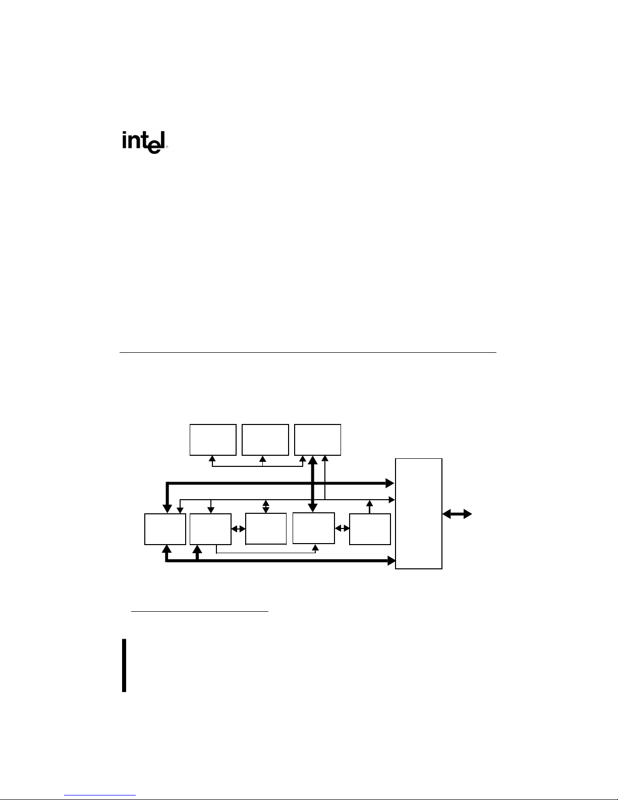
Figure
1. The 80960SA Processor’s Highly Parallel Architecture
* Relative to Digital Equipment Corporation’s VAX-11/780 at 1 MIPS (VAX-11™ is a trademark of Digital Equipment
Co
rporation)
■ High-Performance Embedded
Architectu
re
— 20 MIPS* Burst Execution at 20 MHz
— 7.5 MIPS Sustained Execution
at 20 MHz
■ 512-Byte On-Chip Instruction Cache
— Direct Mapped
— Parallel Load/Decode for Uncached
Instr
uctions
■ Multiple Register Sets
— Sixteen Global 32-Bit Registers
— Sixteen Local 32-Bit Registers
— Four Local Register Sets Stored
On-Chip
— Register Scoreboarding
■ Pin Compatible with 80960SB
■ Built-in Interrupt Controller
— 4 Direct Interrupt Pins
— 31 Priority Levels, 256 Vectors
■ Easy to Use, High Bandwidth 16-Bit Bus
— 32 Mbytes/s Burst
— Up to 16 Bytes Transferred per Burst
■ 32-Bit Address Space, 4 Gigabytes
■ 80-Lead Quad Flat Pack (EIAJ QFP)
— 84-Lead Plastic Leaded Chip Carrier
(PL
CC)
■ Software Compatible with
80960KA/KB/CA/CF
Processors
INSTRUCTION
FETCH UNI
T
512-BYTE
INSTRUCTIO
N
CACH
E
INSTRUCTION
DECODER
MICRO
-
INSTRUCTION
SEQ
UENCER
MICRO
-
INSTRUCTION
ROM
32-BIT
BU
S
CONTROL
LOGI
C
32-BIT
INSTRUCTIO
N
EXECUTIO
N
UNI
T
64-
BY 32-BIT
LOCAL
REGISTE
R
CACH
E
SIXTEEN
32-BIT
GLOBAL
REGISTERS
32-BIT
ADDRES
S
16-BIT
BURS
T
BUS
Page 2

ii
CONTENTS PAGE
1.0 THE i960® PROCESSOR ...........................................................................................................................1
1.1 Key Performance Features .................................................................................................................2
1.1.1 Memory Space And Addressing Modes ...................................................................................4
1.1.2 Data Types ...............................................................................................................................4
1.1.3 Large Register Set ...................................................................................................................4
1.1.4 Multiple Register Sets ..............................................................................................................5
1.1.5 Instruction Cache .....................................................................................................................6
1.1.6 Register Scoreboarding ........................................................................................................... 6
1.1.7 High Bandwidth Bus ................................................................................................................6
1.1.8 Interrupt Handling ....................................................................................................................6
1.1.9 Debug Features ....................................................................................................................... 6
1.1.10 Fault Detection .......................................................................................................................7
1.1.11 Built-in Testability ....................................................................................................................7
1.1.12 CHMOS ..................................................................................................................................7
2.0 ELECTRICAL SPECIFICATIONS............................................................................................................. 11
2.1 Power and Grounding .......................................................................................................................11
2.2 Power Decoupling Recommendations .............................................................................................. 11
2.3 Connection Recommendations ......................................................................................................... 11
2.4 Characteristic Curves ....................................................................................................................... 11
2.5 Test Load Circuit ...............................................................................................................................13
2.6 ABSOLUTE MAXIMUM RATINGS* ..................................................................................................14
2.7 DC Characteristics ............................................................................................................................14
2.8 AC Specifications ..............................................................................................................................15
3.0 MECHANICAL DATA................................................................................................................................21
3.1 Packaging .........................................................................................................................................21
3.2 Pin Assignment .................................................................................................................................21
3.3 Pinout ................................................................................................................................................23
3.4 Package Thermal Specifications ......................................................................................................27
3.5 Stepping Register Information ..........................................................................................................27
4.0 WAVEFORMS...........................................................................................................................................28
5.0 REVISION HISTORY ................................................................................................................................34
80960SA
EMBEDDED 32-BIT MICROPROCESSOR
WITH 16-BIT BURST DATA BUS
Page 3

iii
LIST OF FIGURES PAGE
Figure 1 The 80960SA Processor’s Highly Parallel Architecture ................................................................0
Figure 2 80960SA Programming Environment ...........................................................................................1
Figure 3 Instruction Formats ......................................................................................................................4
Figure 4 Multiple Register Sets Are Stored On-Chip ..................................................................................5
Figure 5 Connection Recommendation for LOCK
....................................................................................11
Figure 6 Typical Supply Current vs. Case Temperature ...........................................................................12
Figure 7 Typical Current vs. Frequency (Room Temp) ............................................................................. 12
Figure 8 Typical Current vs. Frequency (Hot Temp) ................................................................................. 13
Figure 9 Capacitive Derating Curve ......................................................................................................... 13
Figure 10 Test Load Circuit for Three-State Output Pins ............................................................................ 13
Figure 11 Drive Levels and Timing Relationships for 80960SA Signals ..................................................... 15
Figure 12 Processor Clock Pulse (CLK2) ...................................................................................................19
Figure 13 RESET
Signal Timing .................................................................................................................19
Figure 14 HOLD Timing ..............................................................................................................................20
Figure 15 80-Lead EIAJ Quad Flat Pack (QFP) Package ..........................................................................21
Figure 16 84-Lead Plastic Leaded Chip Carrier (PLCC) Package .............................................................22
Figure 17 Non-Burst Read and Write Transactions Without Wait States ....................................................28
Figure 18 Quad Word Burst Read Transaction With 1, 0, 0, 0, 0, 0, 0, 0 Wait States ................................29
Figure 19 Burst Write Transaction With 2, 1, 1, 1 Wait States (6-8 Bytes Transferred) ..............................30
Figure 20 Accesses Generated by Quad Word Read Bus Request,
Misaligned One Byte from Quad Word Boundary 1, 0, 0, 0, 0, 0, 0, 0 Wait States.....................31
Figure 21 Interrupt Acknowledge Cycle ......................................................................................................32
Figure 22 Cold Reset Waveform ................................................................................................................ 33
LIST OF TABLES
Table 1 80960SA Instruction Set ..............................................................................................................3
Table 2 Memory Addressing Modes .........................................................................................................4
Table 3 80960SA Pin Description: Bus Signals ........................................................................................8
Table 4 80960SA Pin Description: Support Signals ................................................................................ 10
Table 5 DC Characteristics .....................................................................................................................14
Table 6 80960SA AC Characteristics (10 MHz) ...................................................................................... 16
Table 7 80960SA AC Characteristics (16 MHz) ...................................................................................... 17
Table 8 80960SA AC Characteristics (20 MHz) ...................................................................................... 18
Table 9 80960SA QFP Pinout — In Pin Order ........................................................................................ 23
Table 10 80960SA QFP Pinout — In Signal Order ...................................................................................24
Table 11 80960SA PLCC Pinout — In Pin Order ......................................................................................25
Table 12 80960SA PLCC Pinout — In Signal Order ................................................................................. 26
Table 13 80960SA QFP Package Thermal Characteristics ...................................................................... 27
Table 14 80960SA PLCC Package Thermal Characteristics .................................................................... 27
Table 15 Die Stepping Cross Reference ...................................................................................................27
Page 4

Page 5
1
80960SA
1.0 THE i960® PROCESSOR
The 80960SA is a member of the 32-bit architecture
from Intel known as the i960 processor family. These
microprocessors were especially designed to serve
the needs of embedded applications. The embedded
market includes applications as diverse as industrial
automation, avionics, image processing, graphics
and networking. These types of applications require
high integration, low power consumption, quick
interrupt response times and high performance.
Since time to market is critical, embedded microprocessors need to be easy to use in both hardware and
software designs.
All members of the i960 processor family share a
common core architecture which utilizes RISC
technology so that, except for special functions, the
family members are object-code compatible. Each
new processor in the family adds its own special set
of functions to the core to satisfy the needs of a
specific application or range of applications in the
embedded market.
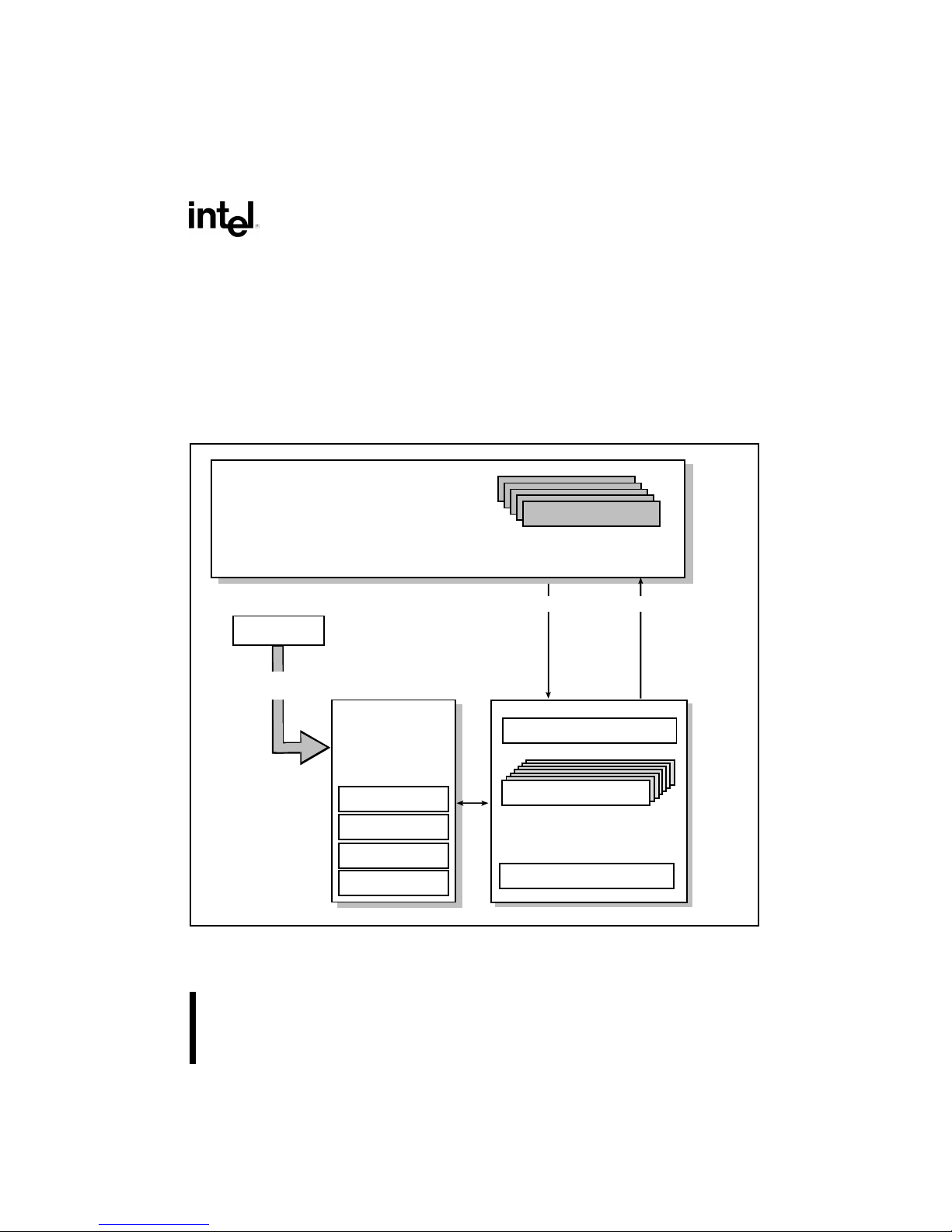
Figure 2. 80960SA Programming Environment
ARCHITECTURALLY
DEFINED
DATA STRUCTURES
FFFF FFFFH
INSTRUCTION
STREAM
INSTRUCTION
EXECUTION
PROCESSOR STATE
REGISTERS
INSTRUCTION
POINTER
ARITHMETIC
CONTROLS
PROCESS
CONTROLS
TRACE
CONTROLS
ADDRESS SPACE
SIXTEEN 32-BIT
GLOBAL REGISTERS
SIXTEEN 32-BIT
LOCAL REGISTERS
g0
g15
r0
r15
LOAD STORE
0000 0000H
INSTRUCTION
CACHE
FETCH
FOUR 80-BIT
CONTROL REGISTERS
FLOATING POINT REGISTERS
Page 6

2
80960SA
1.1 Key Performance Features
The 80960SA architecture is based on the most
recent advances in microprocessor technology and
is grounded in Intel’s long experience in the design
and manufacture of embedded microprocessors.
Many features contribute to the 80960SA’s exceptional performance:
1. Large Register Set. Having a large number of
registers reduces the number of times that a
processor needs to access memory. Modern
compilers can take advantage of this feature to
optimize execution speed. For maximum flexibility, the 80960SA provides thirty-two 32-bit
registers. (See Figure 2.)
2. Fast Instruction Execution. Simple functions
make up the bulk of instructions in most
programs so that execution speed can be
improved by ensuring that these core instructions are executed as quickly as possible. The
most frequently executed instructions — such
as register-register moves, add/subtract,
logical operations and shifts — execute in one
to two cycles. (Table 1 contains a list of instructions.)
3. Load/Store Architecture. One way to improve
execution speed is to reduce the number of
times that the processor must access memory
to perform an operation. As with other
processors based on RISC technology, the
80960SA has a Load/Store architecture. As
such, only the LOAD and STORE instructions
reference memory; all other instructions
operate on registers. This type of architecture
simplifies instruction decoding and is used in
combination with other techniques to increase
parallelism.
4. Simple Instruction Formats. All instructions
in the 80960SA are 32 bits long and must be
aligned on word boundaries. This alignment
makes it possible to eliminate the instruction
alignment stage in the pipeline. To simplify the
instruction decoder, there are only five
instruction formats; each instruction uses only
one format. (See Figure 3.)
5. Overlapped Instruction Execution. Load
operations allow execution of subsequent
instructions to continue before the data has
been returned from memory, so that these
instructions can overlap the load. The
80960SA manages this process transparently
to software through the use of a register scoreboard. Conditional instructions also make use
of a scoreboard so that subsequent unrelated
instructions may be executed while the conditional instruction is pending.
6. Integer Execution Optimization. When the
result of an arithmetic execution is used as an
operand in a subsequent calculation, the value
is sent immediately to its destination register.
At the same time, the value is put on a bypass
path to the ALU, thereby saving the time that
otherwise would be required to retrieve the
value for the next operation.
7. Bandwidth Optimizations. The 80960SA gets
optimal use of its memory bus bandwidth
because the bus is tuned for use with the onchip instruction cache: instruction cache line
size matches the maximum burst size for
instruction fetches. The 80960SA automatically
fetches four words in a burst and stores them
directly in the cache. Due to the size of the
cache and the fact that it is continually filled in
anticipation of needed instructions in the
program flow, the 80960SA is relatively insensitive to memory wait states. The benefit is that
the 80960SA delivers outstanding performance
even with a low cost memory system.
8. Cache Bypass. If a cache miss occurs, the
processor fetches the needed instruction then
sends it on to the instruction decoder at the
same time it updates the cache. Thus, no extra
time is spent to load and read the cache.
Page 7

3
80960SA
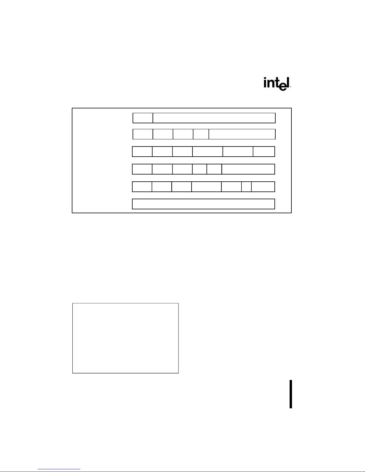
Table 1. 80960SA Instruction Set
Data Movement Arithmetic Logical Bit and Bit Field
Load
Store
Move
Load Address
Add
Subtract
Multiply
Divide
Remainder
Modulo
Shift
Extended Multiply
Extended Divide
And
Not And
And Not
Or
Exclusive Or
Not Or
Or Not
Nor
Exclusive Nor
Not
Nand
Rotate
Set Bit
Clear Bit
Not Bit
Check Bit
Alter Bit
Scan For Bit
Scan Over Bit
Extract
Modify
Comparison Branch Call/Return Fault
Compare
Conditional Compare
Compare and Increment
Compare and Decrement
Unconditional Branch
Conditional Branch
Compare and Branch
Call
Call Extended
Call System
Return
Branch and Link
Conditional Fault
Synchronize Faults
Debug Miscellaneous Decimal
Modify Trace Controls
Mark
Force Mark
Atomic Add
Atomic Modify
Flush Local Registers
Modify Arithmetic
Controls
Scan Byte for Equal
Test Condition Code
Move
Add with Carry
Subtract with Carry
Synchronous
Synchronous Load
Synchronous Move
Page 8
4
80960SA
Figure 3. Instruction Formats
Control
Compare and
Branch
Register to
Register
Memory Access--Short
Memory Access--Long
Opcode Displacement
Opcode DisplacementReg/Lit Reg M
Displacement
Opcode
Opcode
Opcode Reg
Reg
Reg Reg/Lit
Base
Base
M
Modes
Mode
Ext’d Op Reg/Lit
X Offset
Scale xx Offset
1.1.1 Memory Space And Addressing Modes
The 80960SA offers a linear programming
environment so that all programs running on the
processor are contained in a single address space.
Maximum address space size is 4 Gigabytes (2
32
bytes).
For ease of use the 80960SA has a small number of
addressing modes, but includes all those necessary
to ensure efficient execution of high-level languages
such as C. Table 2 lists the memory addressing
modes.
Table 2. Memory Addressing Modes
• 12-Bit Offset
• 32-Bit Offset
• Register-Indirect
• Register + 12-Bit Offset
• Register + 32-Bit Offset
• Register + (Index-Register x Scale-Factor)
• Register x Scale Factor + 32-Bit Displacement
• Register + (Index-Register x Scale-Factor) + 32Bit Displacement
Scale-Factor is 1, 2, 4, 8 or 16
1.1.2 Data Types
The 80960SA recognizes the following data types:
Numeric:
• 8-, 16-, 32- and 64-bit ordinals
• 8-, 16-, 32- and 64-bit integers
Non-Numeric:
• Bit
• Bit Field
• Triple Word (96 bits)
• Quad-Word (128 bits)
1.1.3 Large Register Set
The 80960SA programming environment includes a
large number of registers. In fact, 32 registers are
available at any time. The availability of this many
registers greatly reduces the number of memory
accesses required to perform algorithms, which
leads to greater instruction processing speed.
There are two types of general-purpose register:
local and global. The global registers consist of
sixteen 32-bit registers (g0 though g15). These
registers perform the same function as the general-
Page 9
5
80960SA
purpose registers provided in other popular microprocessors. The term global refers to the fact that
these registers retain their contents across
procedure calls.
The local registers, on the other hand, are procedure
specific. For each procedure call, the 80960SA
allocates 16 local registers (r0 through r15). Each
local register is 32 bits wide.
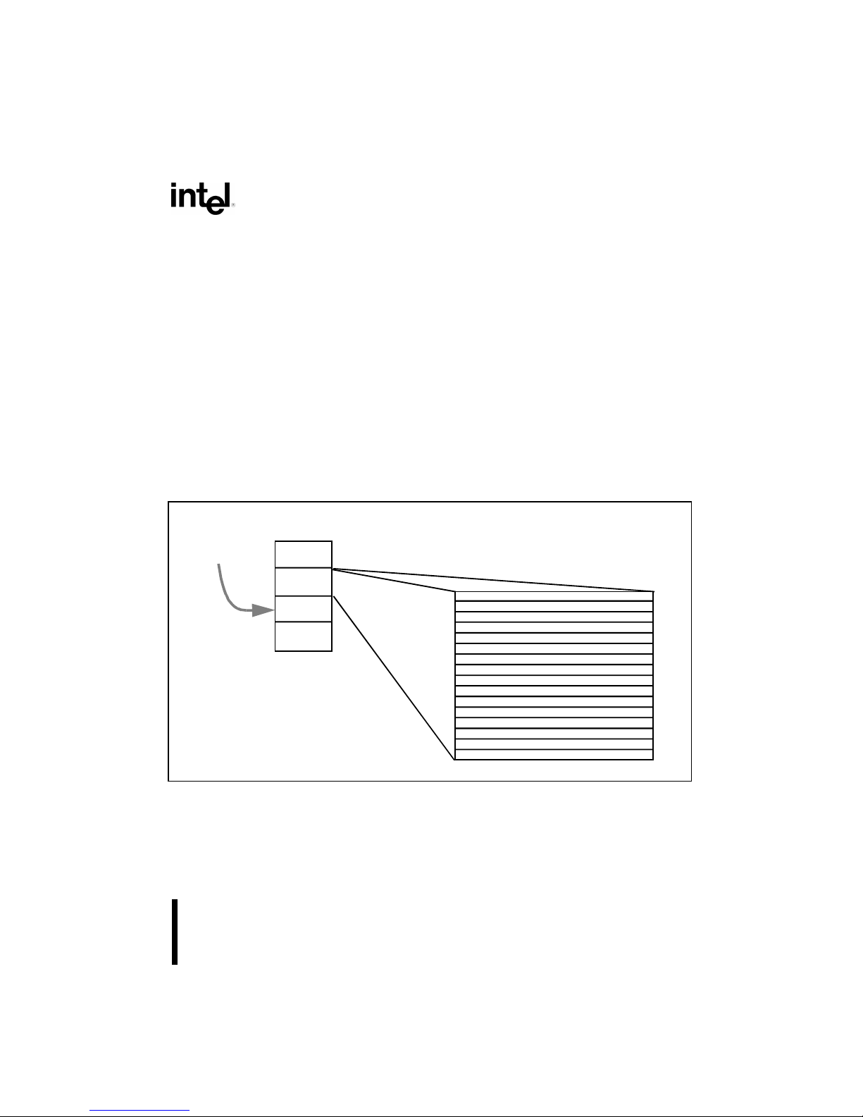
1.1.4 Multiple Register Sets
To further increase the efficiency of the register set,
multiple sets of local registers are stored on-chip
(See Figure 4). This cache holds up to four local
register frames, which means that up to three
procedure calls can be made without having to
access the procedure stack resident in memory.
Although programs may have procedure calls nested
many calls deep, a program typically oscillates back
and forth between only two to three levels. As a
result, with four stack frames in the cache, the probability of having a free frame available on the cache
when a call is made is very high. In fact, runs of
representative C-language programs show that 80%
of the calls are handled without needing to access
memory.
If four or more procedures are active and a new
procedure is called, the 80960SA moves the oldest
local register set in the stack-frame cache to a
procedure stack in memory to make room for a new
set of registers. Global register g15 is the frame
pointer (FP) to the procedure stack.
Global registers are not exchanged on a procedure
call, but retain their contents, making them available
to all procedures for fast parameter passing.
Figure 4. Multiple Register Sets Are Stored On-Chip
r
15
r
0
31
0
ONE OF FOUR
LOCAL
REGISTER SETS
REGISTER
CACHE
LOCAL REGISTER SET
Page 10

6
80960SA
1.1.5 Instruction Cache
To further reduce memory accesses, the 80960SA
includes a 512-byte on-chip instruction cache. The
instruction cache is based on the concept of locality
of reference; most programs are not usually
executed in a steady stream but consist of many
branches, loops and procedure calls that lead to
jumping back and forth in the same small section of
code. Thus, by maintaining a block of instructions in
cache, the number of memory references required to
read instructions into the processor is greatly
reduced.
To load the instruction cache, instructions are
fetched in 16-byte blocks; up to four instructions can
be fetched at one time. An efficient prefetch
algorithm increases the probability that an instruction
will already be in the cache when it is needed.
Code for small loops often fits entirely within the
cache, leading to a great increase in processing
speed since further memory references might not be
necessary until the program exits the loop. Similarly,
when calling short procedures, the code for the
calling procedure is likely to remain in the cache so it
will be there on the procedure’s return.
1.1.6 Register Scoreboarding
The instruction decoder is optimized in several ways.
One optimization method is the ability to overlap
instructions by using register scoreboarding.
Register scoreboarding occurs when a LOAD moves
a variable from memory into a register. When the
instruction initiates, a scoreboard bit on the target
register is set. Once the register is loaded, the bit is
reset. In between, any reference to the register
contents is accompanied by a test of the scoreboard
bit to ensure that the load has completed before
processing continues. Since the processor does not
need to wait for the LOAD to complete, it can execute
additional instructions placed between the LOAD
and the instruction that uses the register contents, as
shown in the following example:
ld data_2, r4
ld data_2, r5
Unrelated instruction
Unrelated instruction
add r4, r5, r6
In essence, the two unrelated instructions between
LOAD and ADD are executed “for free” (i.e., take no
apparent time to execute) because they are
executed while the register is being loaded. Up to
three load instructions can be pending at one time
with three corresponding scoreboard bits set. By
exploiting this feature, system programmers and
compiler writers have a useful tool for optimizing
execution speed.
1.1.7 High Bandwidth Bus
The 80960SA CPU resides on a high-bandwidth
address/data bus. The bus provides a direct communication path between the processor and the
memory and I/O subsystem interfaces. The
processor uses the bus to fetch instructions,
manipulate memory and respond to interrupts. Bus
features include:
• 16-bit data path multiplexed onto the lower bits of
the 32-bit address path
• Eight 16-bit half-word burst capability which
allows transfers from 1 to 16 bytes at a time
• High bandwidth reads and writes with 32
Mbytes/s burst (at 20 MHz)
Table 3 defines bus signal names and functions;
Table 4 defines other component-support signals
such as interrupt lines.
1.1.8 Interrupt Handling
The 80960SA can be interrupted in one of two ways:
by the activation of one of four interrupt pins or by
sending a message on the processor’s data bus.
The 80960SA is unusual in that it automatically
handles interrupts on a priority basis and can keep
track of pending interrupts through its on-chip
interrupt controller. Two of the interrupt pins can be
configured to provide 8259A-style handshaking for
expansion beyond four interrupt lines.
1.1.9 Debug Features
The 80960SA has built-in debug capabilities. There
are two types of breakpoints and six trace modes.
Debug features are controlled by two internal 32-bit
registers, the Process-Controls Word and the TraceControls Word. By setting bits in these control words,
a software debug monitor can closely control how
the processor responds during program execution.
Page 11

7
80960SA
The 80960SA provides two hardware breakpoint
registers on-chip which, by using a special
command, can be set to any value. When the
instruction pointer matches either breakpoint register
value, the breakpoint handling routine is automatically called.
The 80960SA also provides software breakpoints
through the use of two instructions: MARK and
FMARK. These can be placed at any point in a
program and cause the processor to halt execution
at that point and call the breakpoint handling routine.
The breakpoint mechanism is easy to use and
provides a powerful debugging tool.
Tracing is available for instructions (single step
execution), calls and returns and branching. Each
trace type may be enabled separately by a special
debug instruction. In each case, the 80960SA
executes the instruction first and then calls a trace
handling routine (usually part of a software debug
monitor). Further program execution is halted until
the routine completes, at which time execution
resumes at the next instruction. The 80960SA’s
tracing mechanisms, implemented completely in
hardware, greatly simplify the task of software test
and debug.
1.1.10 Fault Detection
The 80960SA has an automatic mechanism to
handle faults. Fault types include trace and
arithmetic faults. When the processor detects a fault,
it automatically calls the appropriate fault handling
routine and saves the current instruction pointer and
necessary state information to make efficient
recovery possible. Like interrupt handling routines,
fault handling routines are usually written to meet the
needs of specific applications and are often included
as part of the operating system or kernel.
For each of the fault types, there are numerous
subtypes that provide specific information about a
fault. The fault handler can use this specific information to respond correctly to the fault.
1.1.11 Built-in Testability
Upon reset, the 80960SA automatically conducts an
exhaustive internal test of its major blocks of logic.
Then, before executing its first instruction, it does a
zero check sum on the first eight words in memory to
ensure that the memory image was programmed
correctly. If a problem is discovered at any point
during the self-test, the 80960SA asserts its FAIL
pin
and will not begin program execution. Self test takes
approximately 24,000 cycles to complete.
System manufacturers can use the 80960SA’s selftest feature during incoming parts inspection. No
special diagnostic programs need to be written. The
test is both thorough and fast. The self-test capability
helps ensure that defective parts are discovered
before systems are shipped and, once in the field,
the self-test makes it easier to distinguish between
problems caused by processor failure and problems
resulting from other causes.
1.1.12 CHMOS
The 80960SA is fabricated using Intel’s CHMOS IV
(Complementary High Speed Metal Oxide Semiconductor) process. The 80960SA is available at 10 and
16 MHz in the QFP package and at 10, 16 and 20
MHz in the PLCC package.
Page 12
8
80960SA
Table 3. 80960SA Pin Description: Bus Signals (Sheet 1 of 2)
NAME TYPE DESCRIPTION
CLK2 I SYSTEM CLOCK provides the fundamental timing for 80960SA systems. It is
divided by two inside the 80960SA to generate the internal processor clock.
A31:16 O
T.S.
ADDRESS BUS carries the upper 16 bits of the 32-bit physical address to memory.
It is valid throughout the burst cycle; no latch is required.
AD15:1, D0 I/O
T.S.
ADDRESS/DATA BUS carries the low order 32-bit addresses and 16-bit data to
and from memory. AD15:4 must be latched since the cycle following the address
cycle carries data on the bus.
A3:1 O
T.S.
ADDRESS BUS carries the word addresses of the 32-bit address to memory.
These three bits are incremented during a burst access indicating the next word
address of the burst access. Note that A3:1 are duplicated with AD3:1 during the
address cycle.
ALE O
T.S.
ADDRESS LATCH ENABLE indicates the transfer of a physical address. ALE is
asserted during a T
a
cycle and deasserted before the beginning of the Td state. It is
active HIGH and floats to a high impedance state during a hold cycle (T
h
).
AS
O
T.S.
ADDRESS STATUS indicates an address state. AS is asserted every Ta state and
deasserted during the following T
d
state. AS is driven HIGH during reset.
W/R
O
T.S.
WRITE/READ specifies, during a Ta cycle, whether the operation is a write or read.
It is latched on-chip and remains valid during T
d
cycles.
DEN
O
T.S.
DATA ENABLE is asserted during Td cycles and indicates transfer of data on the
AD lines. The AD lines should not be driven by an external source unless DEN
is
asserted. When DEN
is asserted, outputs from the previous cycle are guaranteed
to be three-stated. In addition, DEN
deasserted indicates inputs have been
captured; therefore input hold times can be disregarded. DEN
is driven HIGH
during reset.
DT/R
O
T.S.
DATA TRANSMIT / RECEIVE indicates the direction of data transfer to and from
the bus. It is low during T
a
and Td cycles for a read or interrupt acknowledgment; it
is high during T
a
and Td cycles for a write. DT/R never changes state when DEN is
asserted. DT/R
is driven HIGH during reset.
READY
I READY indicates that data on AD lines can be sampled or removed. If READY is
not asserted during a T
d
cycle, the Td cycle is extended to the next cycle by
inserting a wait state (T
w
).
I/O = Input/Output, O = Output, I = Input, O.D. = Open Drain, T.S. = Three-state
Page 13

9
80960SA
LOCK I/O
O.D.
BUS LOCK prevents bus masters from gaining control of the bus during
Read/Modify/Write (RMW) cycles. The processor or any bus agent may assert
LOCK
.
At the start of a RMW operation, the processor examines the LOCK
pin. If the pin is
already asserted, the processor waits until it is not asserted. If the pin is not
asserted, the processor asserts LOCK
during the Ta cycle of the read transaction.
The processor deasserts LOCK
in the Ta cycle of the write transaction. While LOCK
is asserted, a bus agent can perform a normal read or write but not a RMW
operation. The processor also asserts LOCK
during interrupt-acknowledge transac-
tions.
Do not leave LOCK
unconnected. It must be pulled high for the processor to
function properly.
ONCE MODE: The LOCK
pin is sampled during reset. If it is asserted LOW at the
end of reset, all outputs will be three-stated until the part is reset again. ONCE
mode is used in conjunction with an in-circuit emulator.
BE1:0
O
T.S.
BYTE ENABLE LINES specify which data bytes (up to two) on the bus take part in
the current bus cycle. BE1
corresponds to AD15:8; BE0 corresponds to AD7:1, D0.
The byte enable lines are asserted appropriately during each data cycle.
INITIALIZATION FAILURE indicates that the processor has failed to initialize
correctly. The failure state is indicated by a combination of BLAST
asserted and
BE1:0
not asserted. This condition occurs after RESET is deasserted and before
the first bus transaction begins. FAIL
is asserted while the processor performs a
self-test. If the self-test completes successfully, FAIL
is deasserted. The processor
then performs a zero checksum on the first eight words of memory, If it fails, FAIL
is
asserted for a second time and remains asserted; if it passes, system initialization
continues and FAIL
remains deasserted.
HOLD I HOLD indicates a request from an external bus master to acquire the bus. When
the processor receives HOLD and grants bus control to another master, it floats its
three-state bus lines, then asserts HLDA and enters the T
h
state. When HOLD is
deasserted, the processor deasserts HLDA and enters the T
i
or Ta state.
HLDA O
T.S.
HOLD ACKNOWLEDGE notifies an external bus master that the processor has
relinquished control of the bus. This signal is always driven. At reset it is driven
LOW.
BLAST
/FAIL O
T.S.
BURST LAST indicates the last data cycle (Td) of a burst access. It is asserted low
during the last T
d
and associated with Twcycles in a burst access.
INITIALIZATION FAILURE indicates that the processor has failed to initialize
correctly. The failure state is indicated by a combination of BLAST
asserted and
BE1:0
not asserted. This condition occurs after RESET is deasserted and before
the first bus transaction begins. FAIL
is asserted while the processor performs a
self-test. If the self-test completes successfully, FAIL
is deasserted. The processor
then performs a zero checksum on the first eight words of memory, If it fails, FAIL
is
asserted for a second time and remains asserted; if it passes, system initialization
continues and FAIL
remains deasserted.
Table 3. 80960SA Pin Description: Bus Signals (Sheet 2 of 2)
NAME TYPE DESCRIPTION
I/O = Input/Output, O = Output, I = Input, O.D. = Open Drain, T.S. = Three-state
Page 14

10
80960SA
Table 4. 80960SA Pin Description: Support Signals
NAME TYPE DESCRIPTION
RESET
I RESET clears the processor’s internal logic and causes it to reinitialize.
During RESET
assertion, the input pins are ignored (except for INT0, INT1, INT3,
LOCK
), the three-state output pins are placed in a HIGH impedance state (except
for DT/R
, DEN, and AS) and other output pins are placed in their non-asserted
states.
RESET
must be asserted for at least 41 CLK2 cycles for a predictable reset.
Optionally, for a synchronous reset, the LOW and HIGH transition of RESET
should occur after the rising edge of both CLK2 and the external bus CLK and
before the next rising edge of CLK2.
The interrupt pins indicate the initialization sequence executed. Typical initialization requires driving only INT0
and INT3 to a HIGH state. The reset conditions
follow:
INT0
INT1 INT3 LOCK Action Taken
1 x 1 1 Run self test (core initialization)
0 0 1 1 Disable self-test
0 1 x x Reserved
x x 0 x Reserved
x x x 0 ONCE mode (see LOCK
pin)
INT0
I INTERRUPT 0 indicates a pending interrupt. To signal an interrupt in a
synchronous system, this pin — as well as the other interrupt pins — must be
enabled by being deasserted for at least one bus cycle and then asserted for at
least one additional bus cycle. In an asynchronous system, the pin must remain
deasserted for at least two system clock cycles and then asserted for at least two
more system clock cycles. The interrupt control register must be programmed with
an interrupt vector before using this pin.
INT0
is sampled during reset to determine if the self-test sequence is to be
executed.
INT1 I INTERRUPT 1, like INT0
, provides direct interrupt signaling. INT1 is sampled
during reset to determine if the self-test sequence is to be executed.
INT2/INTR I INTERRUPT2/INTERRUPT REQUEST: The interrupt control register determines
how this pin is interpreted. If INT2, it has the same interpretation as the INT0
and
INT1 pins. If INTR, it is used to receive an interrupt request from an external
interrupt controller.
INT3
/INTA I/O
T.S.
INTERRUPT3/INTERRUPT ACKNOWLEDGE: The interrupt control register
determines how this pin is interpreted. If INT3
, it has the same interpretation as
the INT0
and INT1 pins. If INTA, it is used as an output to control interrupt
acknowledge transactions. The INTA
output is latched on-chip and remains valid
during T
d
cycles; as an output, it is open-drain. INT3 must be pulled HIGH during
reset.
NC N/A NOT CONNECTED indicates pins should not be connected. Never connect any
pin marked NC; these pins may be reserved for factory use.
I/O = Input/Output, O = Output, I = Input, O.D. = Open Drain, T.S. = Three-state
Page 15

11
80960SA
2.0 ELECTRICAL SPECIFICATIONS
2.1 Power and Grounding
The 80960SA is implemented in CHMOS IV
technology and therefore has modest power requirements. Its high clock frequency and numerous output
buffers (address/data, control, error and arbitration
signals) can cause power surges as multiple output
buffers simultaneously drive new signal levels. For
clean on-chip power distribution, V
CC
and VSS pins
separately feed the device’s functional units. Power
and ground connections must be made to all
80960SA power and ground pins. On the circuit
board, all V
CC
pins must be strapped closely
together, preferably on a power plane; all V
SS
pins
should be strapped together, preferably on a ground
plane.
2.2 Power Decoupling
Recommendations
Place a liberal amount of decoupling capacitance
near the 80960SA. When driving the bus the
processor can cause transient power surges, particularly when connected to a large capacitive load.
Low inductance capacitors and interconnects are
recommended for best high frequency electrical
performance. Inductance is reduced by shortening
board traces between the processor and decoupling
capacitors as much as possible.
2.3 Connection Recommendations
For reliable operation, always connect unused inputs
to an appropriate signal level. In particular, if one or
more interrupt lines are not used, they should be
pulled up. No inputs should ever be left floating.
The LOCK
open-drain pin requires a pullup resistor
whether or not the pin is used as an output. Figure 5
shows the recommended resistor value.
Do not connect external logic to pins marked NC.
Figure 5. Connection Recommendation
for LOCK
2.4 Characteristic Curves
Figure 6 shows typical supply current requirements
over the operating temperature range of the
processor at supply voltage (V
CC
) of 5V. Figure 7
shows the typical power supply current (I
CC
) that the
80960SA requires at various operating frequencies
when measured at three input voltage (V
CC
) levels.
For a given output current (I
OL
) the curve in Figure 8
shows the worst case output low voltage (V
OL
).
Figure 9 shows the typical capacitive derating curve
for the 80960SA measured from 1.5V on the system
clock (CLK) to 0.8V on the falling edge and 2.0V on
the rising edge of the bus address/data (AD) signals.
910Ω
V
CC
OPEN-DRAIN
OUTPUT
Page 16

12
80960SA
Figure 6. Typical Supply Current vs. Case Temperature
Figure 7. Typical Current vs. Frequency (Room Temp)
VCC = 5.0V
POWER SUPPLY CURRENT (mA)
CASE TEMPERATURE (°C)
20 MHz
16 MHz
10 MHz
100
150
200
250
300
350
-10 0 10 20 30 40 50 60 70 80 90 100 110
0 5 10 15 20 25
OPERATING FREQUENCY (MHz)
4.5V
5.0V
5.5V
TYPICAL SUPPLYCURRENT (mA)
TEMP = +22°C
250
225
200
175
150
125
100
Page 17

13
80960SA
Figure 8. Typical Current vs. Frequency
(Hot Temp)
0 5 10 15 20 25
OPERATING FREQUENCY (MHz)
TYPICAL SUPPLYCURRENT (mA)
TEMP = +85°C
4.5V
5.0V
5.5V
300
250
200
150
100
50
0
Figure 9. Capacitive Derating Curve
0 20 40 60 80 100
30
25
20
15
10
THREE-STATE OUTPUT
CAPACITIVE LOAD (pF)
(TEMP = +85°C, V
CC
= 4.5V)
5
0
RISING
FALLING
X
X
X
VALID DELAY (NS)
2.5 Test Load Circuit
Figure 10 illustrates the load circuit used to test the 80960SA’s output pins.
Figure 10. Test Load Circuit for Three-State Output Pins
THREE-STATE OUTPUT
C
L
= 50 pF for all signals
C
L
Page 18

14
80960SA
2.6 ABSOLUTE MAXIMUM RATINGS*
Parameter Maximum Rating
Operating Temperature (PLCC) ........... 0°C to +85°C Case
Operating Temperature (QFP)............ 0°C to +100°C Case
Storage Temperature .............................. –65°C to +150°C
Voltage on Any Pin (PLCC)................. –0.5V to VCC +0.5V
Voltage on Any Pin (QFP)............... –0.25V to VCC +0.25V
Power Dissipation ....................................... 1.9W (20 MHz)
NOTICE: This is a production data sheet. The
specifications are subject to change without notice.
*WARNING: Stressing the device beyond the
“Absolute Maximum Ratings” may cause
permanent damage. These are stress ratings only.
Operation beyond the “Operating Conditions” is not
recommended and extended exposure beyond the
“Operating Conditions” may affect device reliability.
2.7 DC Characteristics
80960SA (10 and 16 MHz QFP) T
CASE
= 0°C to +100°C, VCC = 5V ± 5%
80960SA (10 and 16 MHz PLCC) T
CASE
= 0°C to +85°C, VCC = 5V ± 10%
80960SA (20 MHz PLCC) T
CASE
= 0°C to +85°C, VCC = 5V ± 5%
Table 5. DC Characteristics
Symbol Parameter Min Max Units Notes
V
IL
Input Low Voltage –0.3 +0.8 V
V
IH
Input High Voltage 2.0 VCC + 0.3 V
V
CL
CLK2 Input Low Voltage –0.3 +0.8 V
V
CH
CLK2 Input High Voltage 0.7 V
CC
VCC + 0.3 V
V
OL
Output Low Voltage 0.45
0.45
VVIOL = 4.0 mA
I
OL
= 6 mA, LOCK Pin
V
OH
Output High Voltage 2.4 V All TS, -2.5 mA(1)
I
CC
Power Supply Current:
10 MHz-QFP
10 MHz-PLCC
16 MHz-PLCC
20 MHz-PLCC
240
240
300
340
mA
mA
mA
mA
T
CASE
= 00C
T
CASE
= 00C
T
CASE
= 00C
T
CASE
= 00C
I
LI1
Input Leakage Current,
Except INT0
, LOCK
±15 µA 0 ≤ VIN≤ V
CC
I
LI2
Input Leakage Current,
INT0
, LOCK
–300 µA VIN= 0.45V (2)
I
OL
Output Leakage Current ±15 µA
C
IN
Input Capacitance 10 pF fC = 1 MHz (3)
C
O
Output Capacitance 12 pF fC = 1 MHz (3)
C
CLK
Clock Capacitance 10 pF fC = 1 MHz (3)
NOTES:
1. Not measured for open-drain output.
2. INT0
and LOCK have internal pullup devices.
3. Input, output and clock capacitance are not tested.
Page 19

15
80960SA
2.8 AC Specifications
This section describes the AC specifications for the
80960SA pins. All input and output timings are
specified relative to the 1.5V level of the rising edge
of CLK2 and refer to the time at which the signal
crosses 1.5V (for output delay and input setup). All
AC testing should be done with input voltages of
0.4V and 2.4V, except for the clock (CLK2) which
should be tested with input voltages of 0.45V and 0.7
x V
CC
. See Figure 11 and Tables 6, 7 and 8 for timing
relationships for the 80960SA signals.
Figure 11. Drive Levels and Timing Relationships for 80960SA Signals
A B C D A B C
1.5V
1.5V 1.5V 1.5V
T
6
1.5V
1.5V
T
7
1.5V 1.5VVALID OUTPUT
T
6
T
8
T
8
T
13
T
14
1.5V 1.5V
VALID OUTPUT
T
9
2.0V 2.0V
2.0V 2.0V
0.8V 0.8V
0.8V 0.8V
EDGE
CLK2
OUTPUTS:
AD15:1, A3:1, D0,
W/R
, DEN, BLAST,
HLDA, LOCK
, INTA
ALE
DT/R
INPUTS:
AD15:1, D0,
INT2, INT3
HOLD
LOCK
READY
T
9
T
10
T
11
T
12
T
11
A 31:16, BE1:0,
INT0, INT1,
AS
T
6AS
T
6AS
VALID INPUT
Page 20

16
80960SA
Table 6. 80960SA AC Characteristics (10 MHz)
Symbol Parameter Min Max Units Notes
Input Clock
T
1
Processor Clock Period (CLK2) 50 125 ns VIN= 1.5V
T
2
Processor Clock Low Time (CLK2) 8 ns VT= 10% Point
= V
CL
+ (VCH – VCL) x 0.1
T
3
Processor Clock High Time
(CLK2)
8 ns VT= 90% Point
= V
CL
+ (VCH – VCL) x 0.9
T
4
Processor Clock Fall Time (CLK2) 10 ns VT= 90% to 10% Point (1)
T
5
Processor Clock Rise Time (CLK2) 10 ns VT= 10% to 90% Point (1)
Synchronous Outputs
T
6
Output Valid Delay 2 31 ns
T
6AS
AS Output Valid Delay 2 25 ns
T
7
ALE Width T1 - 11 ns
T
8
ALE Output Valid Delay 4 33 ns
T
9
Output Float Delay 2 20 ns (2)
Synchronous Inputs
T
10
Input Setup 1 10 ns
T
11
Input Hold 2 ns
T
12
Input Setup 2 13 ns
T
13
Setup to ALE Inactive 10 ns
T
14
Hold after ALE Inactive 8 ns
T
15
RESET Hold 3 ns (3)
T
16
RESET Setup 5 ns (3)
T
17
RESET Width 2050 ns 41 CLK2 Periods Minimum
NOTES:
1. Processor clock (CLK2) rise time and fall time are not tested.
2. A float condition occurs when the maximum output current becomes less than I
LO
. Float delay is not tested, but should be
no longer than the valid delay.
3. Meeting RESET
setup and hold times is an optional method of synchronizing your clocks. If you decide to use an asyn-
chronous reset, synchronizing the clock can be accomplished by using AS
.
Page 21

17
80960SA
Table 7. 80960SA AC Characteristics (16 MHz)
Symbol Parameter Min Max Units Notes
Input Clock
T
1
Processor Clock Period (CLK2) 31.25 125 ns VIN= 1.5V
T
2
Processor Clock Low Time (CLK2) 8 ns VT= 10% Point
= V
CL
+ (VCH – VCL) x 0.1
T
3
Processor Clock High Time
(CLK2)
8 ns VT= 90% Point
= V
CL
+ (VCH – VCL) x 0.9
T
4
Processor Clock Fall Time (CLK2) 10 ns VT= 90% to 10% Point (1)
T
5
Processor Clock Rise Time (CLK2) 10 ns VT= 10% to 90% Point (1)
Synchronous Outputs
T
6
Output Valid Delay 2 25 ns
T
6AS
AS Output Valid Delay 2 21 ns
T
7
ALE Width T1 - 11 ns
T
8
ALE Output Valid Delay 2 22 ns
T
9
Output Float Delay 2 20 ns (2)
Synchronous Inputs
T
10
Input Setup 1 10 ns
T
11
Input Hold 2 ns
T
12
Input Setup 2 13 ns
T
13
Setup to ALE Inactive 10 ns
T
14
Hold after ALE Inactive 8 ns
T
15
RESET Hold 3 ns (3)
T
16
RESET Setup 5 ns (3)
T
17
RESET Width 1281 ns 41 CLK2 Periods Minimum
NOTES:
1. Processor clock (CLK2) rise time and fall time are not tested.
2. A float condition occurs when the maximum output current becomes less than I
LO
. Float delay is not tested, but should be
no longer than the valid delay.
3. Meeting RESET
setup and hold times is an optional method of synchronizing your clocks. If you decide to use an asyn-
chronous reset, synchronizing the clock can be accomplished by using AS
.
Page 22

18
80960SA
Table 8. 80960SA AC Characteristics (20 MHz)
Symbol Parameter Min Max Units Notes
Input Clock
T
1
Processor Clock Period (CLK2) 25 125 ns VIN= 1.5V
T
2
Processor Clock Low Time (CLK2) 6 ns VT= 10% Point
= V
CL
+ (VCH – VCL) x 0.1
T
3
Processor Clock High Time (CLK2) 6 ns VT= 90% Point
= V
CL
+ (VCH – VCL) x 0.9
T
4
Processor Clock Fall Time (CLK2) 10 ns VT= 90% to 10% Point (1)
T
5
Processor Clock Rise Time (CLK2) 10 ns VT= 10% to 90% Point (1)
Synchronous Outputs
T
6
Output Valid Delay 2 20 ns
T
6AS
AS Output Valid Delay 2 20 ns
T
7
ALE Width T1 - 11 ns
T
8
ALE Output Valid Delay 2 18 ns
T
9
Output Float Delay 2 17 ns (2)
Synchronous Inputs
T
10
Input Setup 1 7 ns
T
11
Input Hold 2 ns
T
12
Input Setup 2 13 ns
T
13
Setup to ALE Inactive 10 ns
T
14
Hold after ALE Inactive 8 ns
T
15
RESET Hold 3 ns (3)
T
16
RESET Setup 5 ns (3)
T
17
RESET Width 1025 ns 41 CLK2 Periods Minimum
NOTES:
1. Processor clock (CLK2) rise time and fall time are not tested.
2. A float condition occurs when the maximum output current becomes less than I
LO
. Float delay is not tested, but should be
no longer than the valid delay.
3. Meeting RESET
setup and hold times is an optional method of synchronizing your clocks. If you decide to use an asyn-
chronous reset, synchronizing the clock can be accomplished by using AS
.
Page 23

19
80960SA
Figure 12. Processor Clock Pulse (CLK2)
Figure 13. RESET
Signal Timing
HIGH LEVEL (MIN) 0.7V
CC
LOW LEVEL (MAX) 0.8V
T
1
T
3
T
5
T
4
T
2
90%
10%
1.5 V
CLK2
CLK
RESET
OUTPUTS
A B C D A
B C
T
15
T
16
INT0, INT1,
INT3
, LOCK
INITIALIZATION PARAMETERS
T
17
NOTE: Initialization parameters must be set up at least four CLK2 periods before the first CLK2 “A” edge.
Page 24

20
80960SA
Figure 14. HOLD Timing
T
h
T
h
T
h
CLK2
CLK
HOLD
HLDA
T
12
T
11
T
6
T
6
Page 25

21
80960SA
3.0 MECHANICAL DATA
3.1 Packaging
The 80960SA is available in two package types:
• 80-lead quad flat pack (EIAJ QFP). Shown in
Figure
15.
• 84-lead plastic leaded chip carrier (PLCC).
Shown
in Figure 16.
Dimensions
for both package types are given in the
Inte
l Packaging handbook (Order #240800).
3.2 Pin Assignment
The QFP and PLCC have different pin assignments.
The QFP pins are numbered in order from 1 to 80
around
the package perimeter. The PLCC pins are
numbered
in order from 1 to 84 around the package
perime
ter. Tables 9 and 10 list the function of each
QFP
pin; Tables 11 and 12 list the function of each
PLCC
pin.
V
CC
and GND connections must be made to multiple
V
CC
and GND pins. Each VCC and GND pin must be
connected
to the appropriate voltage or ground and
externally
strapped close to the package. It is recom-
mended
that you include separate power and ground
plane
s in your circuit board for power distribution.
Pins
identified as NC (No Connect) should never be
connected
.
Figure 15. 80-Lead EIAJ Quad Flat Pack (QFP) Package
AS
AD1
AD
2
V
SS
AD3
AD
4
AD
5
AD
6
A
D
7
AD
8
A
D
9
AD
1
0
AD
1
1
AD
1
2
AD
1
3
A
D
1
4
AD
1
5
A
16
A17A
18
A1
9
A20
A2
1
A2
2
V
SS
A23
A2
4
A25
BLAST
H
O
LD
V
S
S
R
ESET
V
CC
CLK
2
I
N
T3/INT
A
I
N
T
2
/
I
N
T
R
INT1
INT0
V
C
C
V
C
C
NC
V
SS
V
S
S
V
C
C
V
CC
V
S
S
V
SS
V
CC
V
CC
NC
V
SS
V
SS
V
SS
V
CC
V
CC
V
CC
HL
DA
ALE
A1
A2
A3
D0
W
/
R
READY
D
T
/R
B
E0
BE1
V
S
S
LO
CK
D
EN
V
S
S
V
SS
V
C
C
V
C
C
66
65
64 63 62 61 60 59 58 57 56 55 54 53 52 51 50 49 48 47 46 45 44 43 42 41
40
39
38
37
36
35
34
1 2 3 4 5 6 7 8 9 10 11 12 13 14 15 16 17 18 19 20 21
80
79
78
77
76
75
74
73
72
71
70
69
68
67
22 23 24
25
26
27
28
29
30
31
32
33
A26
A2
7
A2
8
A2
9
A3
0
A3
1
x80960SA-20
XXXXXXXX
XXXXX
X
XXXXX
X
NOTE: To address the fact that many of the package prefix variables have changed, all
package prefix variables in this document are now indicated with an "x".
Page 26

22
80960SA
.
Figure
16. 84-Lead Plastic Leaded Chip Carrier (PLCC) Package
AS
AD1
AD
2
V
SS
AD
3
AD
4
AD5
AD
6
AD7
AD
8
AD
9
AD10
AD1
1
AD1
2
AD1
3
AD1
4
AD1
5
A1
6
A17
A1
8
A19
A2
0
A21
A2
2
V
SS
A23
A
2
4
A25
BLAST
HOLD
V
SS
RESET
V
C
C
CLK2
INT3
/INTA
INT2/INTR
INT1
INT0
V
CC
V
C
C
N
C
V
S
S
V
SS
V
CC
V
C
C
V
SS
V
SS
V
CC
V
CC
NC
V
SS
V
SS
NC
V
SS
V
CC
V
CC
V
CC
HLDA
ALE
A
1
A2A
3
D0
W/R
READY
DT/R
B
E
0
B
E
1
V
SS
LOCK
DEN
N
C
N
C
V
S
S
V
S
S
N
C
V
C
C
V
C
C
66
65
64
63
62
61
60
59
58
57
56
55
54
5352515049484746454443424140393837363534
1234567891011
12
13
14
15
16
17
18
19
20
21
84 83 82 81 80 79 78 77 76 75
74
73
72
71
70
69
68
67
22
23
24
25
26
27
28
29
30
31
32
33
A26
A27
A28
A29
A30
A31
x80960SA-20
XXXXXXXX
XXXXX
X
XXXXX
X
NOTE: To address the fact that many of the package prefix variables have changed, all
package prefix variables in this document are now indicated with an "x".
Page 27

23
80960SA
3.3 Pinout
Table 9. 80960SA QFP Pinout — In Pin Order
Pin Signal Pin Signal Pin Signal Pin Signal
1 A22 21 V
CC
41 BE0 61 V
CC
2 A21 22 V
SS
42 V
CC
62 V
SS
3 A20 23 V
CC
43 V
SS
63 NC
4 A19 24 V
SS
44 CLK2 64 AS
5 A18 25 AD6 45 RESET 65 V
SS
6 A17 26 AD5 46 INT0 66 ALE
7 A16 27 AD4 47 INT1 67 READY
8 V
CC
28 AD3 48 INT2/INTR 68 A31
9 V
SS
29 AD2 49 INT3/INTA 69 A30
10 AD15 30 AD1 50 HLDA 70 A29
11 AD14 31 D0 51 V
CC
71 A28
12 V
CC
32 V
SS
52 V
SS
72 V
SS
13 V
SS
33 V
CC
53 HOLD 73 V
CC
14 AD13 34 A3 54 W/R 74 A27
15 AD12 35 A2 55 DEN
75 A26
16 AD11 36 V
CC
56 DT/R 76 A25
17 AD10 37 V
SS
57 BLAST 77 V
CC
18 AD9 38 A1 58 LOCK 78 V
SS
19 AD8 39 NC 59 V
CC
79 A24
20 AD7 40 BE1
60 V
SS
80 A23
NOTES:
Do not connect any external logic to any pins marked NC.
Page 28

24
80960SA
Table 10. 80960SA QFP Pinout — In Signal Order
Signal Pin Signal Pin Signal Pin Signal Pin
A1 38 A18 5 D0 31 V
CC
51
A2 35 A19 4 DEN
55 V
CC
59
A3 34 A20 3 DT/R
56 V
CC
61
AD1 30 A21 2 HLDA 50 V
CC
73
AD2 29 A22 1 HOLD 53 V
CC
77
AD3 28 A23 80 INT0
46 V
CC
8
AD4 27 A24 79 INT1 47 V
SS
13
AD5 26 A25 76 INT2/INTR 48 V
SS
22
AD6 25 A26 75 INT3
/INTA 49 V
SS
24
AD7 20 A27 74 LOCK 58 V
SS
32
AD8 19 A28 71 NC 39 V
SS
37
AD9 18 A29 70 NC 63 V
SS
43
AD10 17 A30 69 READY
67 V
SS
52
AD11 16 A31 68 RESET
45 V
SS
60
AD12 15 ALE 66 V
CC
12 V
SS
62
AD13 14 AS
64 V
CC
21 V
SS
72
AD14 11 BE0
41 V
CC
23 V
SS
78
AD15 10 BE1
40 V
CC
33 V
SS
9
A16 7 BLAST
57 V
CC
36 V
SS
65
A17 6 CLK2 44 V
CC
42 W/R 54
NOTES:
Do not connect any external logic to any pins marked N.C.
Page 29

25
80960SA
Table 11. 80960SA PLCC Pinout — In Pin Order
Pin Signal Pin Signal Pin Signal Pin Signal
1 V
CC
22 V
SS
43 V
SS
64 HOLD
2 NC 23 NC 44 V
CC
65 NC
3 A27 24 AD13 45 A3 66 W/R
4 A26 25 AD12 46 A2 67 DEN
5 A25 26 AD11 47 V
CC
68 DT/R
6 V
CC
27 AD10 48 V
SS
69 BLAST
7 V
SS
28 AD 9 49 A1 70 LOCK
8 A24 29 AD8 50 NC 71 V
CC
9 A23 30 AD7 51 BE1 72 V
SS
10 A2 2 31 V
CC
52 BE0 73 V
CC
11 A2 1 32 V
SS
53 V
CC
74 V
SS
12 A2 0 33 V
CC
54 V
SS
75 NC
13 A1 9 34 V
SS
55 CLK 2 76 AS
14 A1 8 35 AD6 56 RESET 77 V
SS
15 A1 7 36 AD5 57 INT0 78 ALE
16 A1 6 37 AD4 58 INT1 79 READY
17 V
CC
38 AD 3 59 INT2/INTR 80 A31
18 V
SS
39 D2 60 INT3/INTA 81 A30
19 AD1 5 40 D1 61 HLDA 82 A29
20 AD1 4 41 D0 62 V
CC
83 A28
21 V
CC
42 NC 63 V
SS
84 V
SS
NOTES:
Do not connect any external logic to any pins marked NC.
Page 30

26
80960SA
Table 12. 80960SA PLCC Pinout — In Signal Order
Signal Pin Signal Pin Signal Pin Signal Pin
A1 49 A18 14 DT/R
68 V
CC
44
A2 46 A19 13 HLDA 61 V
CC
47
A3 45 A20 12 HOLD 64 V
CC
53
D0 41 A21 11 INT0
57 V
CC
6
AD1 40 A22 10 INT1 58 V
CC
62
AD2 39 A23 9 INT2/INTR 5 9 V
CC
71
AD3 38 A24 8 INT3
/INTA 60 V
CC
73
AD4 37 A25 5 LOCK
70 V
SS
18
AD5 36 A26 4 NC 2 V
SS
22
AD6 35 A27 3 NC 23 V
SS
32
AD7 30 A28 83 NC 42 V
SS
34
AD8 29 A29 82 NC 50 V
SS
43
AD9 28 A30 81 NC 65 V
SS
48
AD10 27 A31 80 NC 75 V
SS
54
AD11 26 ALE 78 READY
79 V
SS
63
AD12 25 AS
76 RESE T 56 V
SS
7
AD13 24 BE0
52 V
CC
1 V
SS
72
AD14 20 BE1
51 V
CC
17 V
SS
74
AD15 19 BLAST
69 V
CC
21 V
SS
77
AD16 16 CLK2 55 V
CC
31 V
SS
84
A17 15 DEN
67 V
CC
33 W/R 66
NOTES:
Do not connect any external logic to any pins marked NC.
Page 31

27
80960SA
3.4 Package Thermal Specifications
The 80960SA is specified for operation when case
temperature is within the range 0°C to +85°C (PLCC)
or 0°C to 100°C (QFP). Measure case temperature
at the top center of the package. Ambient temperature can be calculated from:
T
J
= TC + P*θ
JC
TA = TJ - P*θ
JA
TC = TA + P*[θJA−θJC]
Compute P by multiplying the maximum voltage by
the typical current at maximum temperature. Values
for
θJA and θJC for various airflows are given in Table
13 for the QFP package and in Table 14 for the
PLCC package. I
CC
at maximum temperature is
typically 80 percent of specified I
CC
maximum (cold).
Table 13. 80960SA QFP Package Thermal Characteristics
Thermal Resistance — °C/Watt
Parameter
Airflow — ft./min (m/sec)
0 50 100 200 400 600 800
θ Junction-to-Ambient (Case
measured in the middle of the
top of the package)
(No Heatsink)
59 57 54 50 44 40 38
θ Junction-to-Case
11 11 11 11 11 11 11
NOTES:
This table applies to 80960SA QFP soldered directly to board.
Table 14. 80960SA PLCC Package Thermal Characteristics
Thermal Resistance — °C/Watt
Parameter
Airflow — ft./min (m/sec)
0 50 100 200 400 600 800 1000
θ Junction-to-Ambient
(No Heatsink)
34 32 29.5 28 25 23 21 20.5
θ Junction-to-Case
12 12 12 12 12 12 12 12
NOTES:
This table applies to 80960SA PLCC soldered directly to board.
3.5 Stepping Register Information
Upon reset, register g0 contains die stepping information. Table 15 shows the relationship between the
number in g0 and the current die stepping
The current numbering pattern in g0 may not be
consistent with past or future steppings of this
product.
Table 15. Die Stepping Cross Reference
Register g0 Die Stepping
01010101H C-1
Page 32

28
80960SA
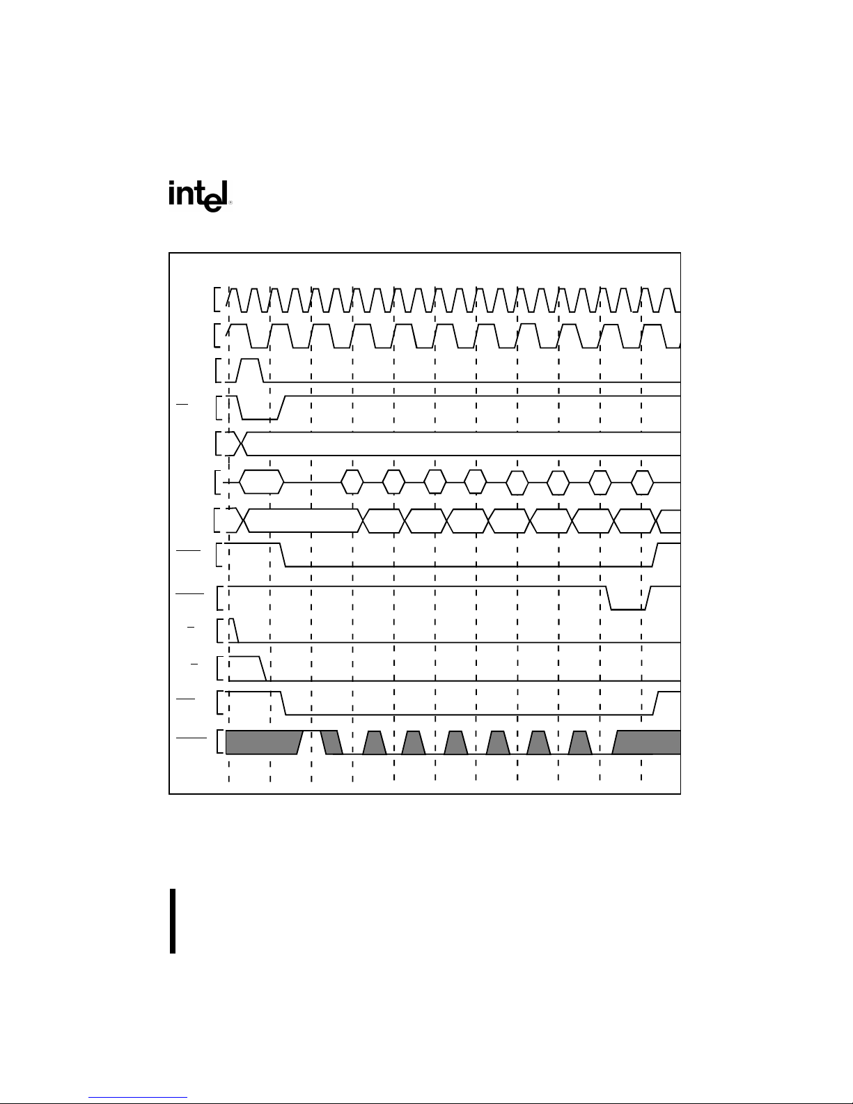
4.0 WAVEFORMS
Figures 17, 18, 19, 20 and 21 show waveforms for various transactions on the 80960SA’s bus. Figure 22 shows
a cold reset functional waveform.
Figure 17. Non-Burst Read and Write Transactions Without Wait States
T
a
T
d
T
r
T
a
T
d
T
r
CLK2
CLK
ALE
AS
A31:16
W/R
DT/R
DEN
READY
BLAST
BE1:0
VALID VALID
INVALID
A3:1
ADDR
ADDR
DATA
D
A15:4,
D15:0
VALID
VALID
Page 33
29
80960SA
Figure 18. Quad Word Burst Read Transaction With 1, 0, 0, 0, 0, 0, 0, 0 Wait States
T
a
T
w
T
d
T
d
T
d
T
d
T
d
T
d
T
d
T
d
T
r
CLK2
CLK
ALE
AS
BE1:0
W/R
DT/R
DEN
READY
BLAST
D D D D D D D D
A3:1
A15:4,
D15:0
A31:16
VALID
000 001 010 011 100 101 110 111
ADDR
Page 34

30
80960SA
Figure 19. Burst Write Transaction With 2, 1, 1, 1 Wait States (6-8 Bytes Transferred)
T
a
T
w
T
w
T
d
T
w
T
d
T
w
T
d
T
w
T
d
T
r
CLK2
CLK
ALE
AS
BE1:0
W/R
DT/R
DEN
READY
BLAST
A3:1
A15:4,
D15:0
A31:16
VALID
ADDR
DATA
DATA
DATA DATA
VALID
VALID VALID
VALID
00 00 x0
0x
Page 35

31
80960SA
Figure 20. Accesses Generated by Quad Word Read Bus Request,
Misaligned One Byte from Quad Word Boundary 1, 0, 0, 0, 0, 0, 0, 0 Wait States
T
a
T
w
T
d
Td Td T
d
T
d
T
d
T
d
T
d
T
r
CLK2
CLK
ALE
AS
BE1
W/R
DT/R
DEN
BLAST
A3:1
A15:4,
D15:0
A31:16
VALID
ADDR
T
a
T
w
T
d
T
r
BE0
ADDR
D D D D D D D D
D
VALID
000
001 010 011 100 101 110 111 000
READY
Page 36

32
80960SA
Figure 21. Interrupt Acknowledge Cycle
CLK2
TaTdTrT
i
TiTiTiTiTaT
w
TdT
r
A15:4,
ALE
AS
INTA
DT/R
DEN
LOCK
CLK
W/R
BLAST
A31:16
D15:0
ADDR
ADD
DATA
A3:1
1 1 0
BE1:0
READY
1 0
1 0
Page 37

33
80960SA
Figure 22. Cold Reset Waveform
RESET
CLK2
CLK
V
CC
AS, DT/R,
DEN,
LOCK (O)
HLDA
BLAST/FAIL
ALE, A31:16,
A15:4, A3:1,
D15:0,
BE1:0, W/R
INT0, INT1,
INT3,
LOCK (I)
VCCand CLK2 stable to RESET high, minimum 41 CLK2 periods
Initialization parameters
set up to first A edge,
minimum 4 CLK2 periods
First
Bus
Activity
Internal self-test,
approximately 94,000 CLK2
periods (if selected)
A B C D T
a
A B C D A B C D
A B C D
A B C D
A B C D
48,000
VALID
Page 38

34
80960SA
5.0 REVISION HISTORY
This data sheet supersedes data sheet 272206-001 and applies only to those devices identified as the current
stepping in section 3.
5. The sections significantly changed since the previous revision are:
Data
sheet 270917-004 applied to both the 80960SA and the 80960SB. The 80960SA was then documented
alone
in data sheet 272206-001. The sections significantly changed between revisions -004 of the SA/SB data
sheet and 272206-001 of the SA data sheet were:
Section
Las
t
Re
v.
Description
2.3
Connection Recommendations (pg. 11) -001 Removed two LOCK
pin Connection Recommendation
figures and added Figure 5 to reflect the new LOCK
pin
connection
recommendation of a single 910
Ω pullup
resistor
.
2.5 Test Load Circuit (pg. 13) -001 Obsolete figure (Test Load Circuit for Open-Drain
Output
Pins) removed to reflect current test conditions.
2.7
DC Characteristics (pg. 14) -001 I
OL
value at 0.45V improved.
WAS
: 2.5 mA IS: 4.0 mA
LOCK
pin IOL value at 0.45V relaxed.
WAS
: 12 mA IS: 6 mA
LOCK
pin IOL value at 0.60V deleted.
80960SA
16 MHz QFP added to product list.
3.5
Stepping Register Information (pg. 27) -001 New section added.
Secti
on
La
st
Re
v.
Descripti
on
2.3 Connection Recommendations
(pg.
11)
-0
04 Deleted corresponding graph of open drain voltage vs. out-
put
current.
Figure 6. Typical Supply Current vs.
Cas
e Temperature (pg. 11)
Figure 7. Typical Current vs. Frequency
(Room Temp) (pg. 12)
Figure 8. Typical Current vs. Frequency
(Hot Temp) (pg. 12)
-0
04 Regraphed new data in three graphs instead of two.
Table 5. DC Characteristics (pg. 15) -004 Input Leakage Current (I
LI2
) Specification added to accu-
rately
describe leakage of INT0 and LOCK as inputs.
ICC max reduced:
Power Supply Current: Was: Is:
10
MHz 280 240
16
MHz 350 300
NOTES:
Page numbers re
fer to 80960SA data sheet number 272206-001.
Overall
To address the fact that many of the package prefix
variables have changed, all package prefix variables
in this document are now indicated with an "x".
-003
Page 39

35
80960SA
Table 6. 80960SA AC Characteristics
(10 MHz) (pg. 17)
Table 7. 80960SA AC Characteristics
(16 MHz) (pg. 18).
-004 T7 minimum specification improved:
Power Supply Current: Was: Is:
10 MHz 24 ns T
1
- 11 ns
16 MHZ 15 ns T
1
- 11 ns
Table 8. 80960SA AC Characteristics
(20 MHz) (pg. 19)
-004 New 20 MHz specification table added for 80960SA C-step.
Table 11. 80960SA PLCC Pinout — In
Pin Order (pg. 26)
-004
θJA increased to reflect smaller die size and lower ICC.
Table 11. 80960SA PLCC Pinout — In
Pin Order (pg. 26)
-004
θJA and θJCincreased to reflect smaller die size and lower
I
CC
.
The sections significantly changed between revisions -003 and -004 of the 80960SA/SB Data Sheet were:
Section
Last
Rev.
Description
DC Characteristics -003 Operating temperature for PLCC package changed:
WAS: T
CASE
= 0°C to +100°C
IS: T
CASE
= 0°C to +85°C
The test program has not changed.
Table 9. 80960SA and 80960SB QFP
Pinout — In Pin Order
-003 Signal A12 incorrectly shown as Pin 28; is now correctly shown as Pin 38. Note added to clarify No Connect Pins.
Section
Last
Rev.
Description
NOTES:
Page numbers refer to 80960SA data sheet number 272206-001.
 Loading...