

Page 1

Intel® 80331 I/O Processor
Design Guide
March 2005
Order Number:273823-003
Page 2

Intel® 80331 I/O Processor Design Guide
Contents
INFORMATION IN THIS DOCUMENT IS PROVIDED IN CONNECTION WITH INTEL® PRODUCTS. NO LICENSE, EXPRESS OR IMPLIED, BY
ESTOPPEL OR OTHERWISE, TO ANY INTELLECTUAL PROPERTY RIGHTS IS GRANTED BY THIS DO CUMENT. EXCEPT AS PROVIDED IN
INTEL'S TERMS AND CONDITIONS OF SALE FOR SUCH PRODUCTS, INTEL ASSUM ES NO LIABILITY WHATSOEVER, AND INTEL DISCLAIMS
ANY EXPRESS OR IMPLIED WARRANTY, RELATING TO SALE AND/ OR USE OF INTEL PRODUCTS INCLUDING LIABILITY OR WARRANTIES
RELATING T O FITNESS FOR A PARTICULAR PURPOSE, MERCHANTABILITY, OR INFRINGEMENT OF ANY PATENT, COPYRIGHT OR OTHER
INTELLECTUAL PROPERTY RIGHT.
Intel products are not intended for use in medical, life saving, life sustaining applications.
Intel may make changes to specifications and product descriptions at any time, without notice.
Contact your local Intel sales office or your distributor to obtain the latest specifications and before placing your product order.
Copies of documents which have an order number and are referenced in this document, or other Intel literature, may be obtained by calling1-800-548-
4725, or by visiting Intel's website at http://www.intel.com.
AlertVIEW, AnyPoint, AppChoice, BoardWatch, BunnyPeople, CablePort, Celeron, Chips, CT Connect, CT Media, Dialogic, DM3, EtherExpress,
ETOX, FlashFile, i386, i486, i960, iCOMP, InstantIP, Intel, Intel logo, Intel386, Intel486, Intel740, IntelDX2, IntelDX4, IntelSX2, Intel Create & Share,
Intel GigaBlade, Intel InBusiness, Intel Inside, Intel Inside logo, Intel NetBurst, Intel NetMerge, Intel NetStructure, Intel Play, Intel Play logo, Intel
SingleDriver, Intel SpeedStep, Intel StrataFlash, Intel TeamStation, Intel Xeon, Intel XScale, IPLink, Itanium, LANDesk, LanRover, MCS, MMX, MMX
logo, Optimizer logo, OverDrive, Paragon, PC Dads, PC Parents, PDCharm, Pentium, Pentium II Xeon, Pentium III Xeon, Performance at Your
Command, RemoteExpress, Shiva, SmartDie, Solutions960, Sound Mark, StorageExpress, The Computer Inside., The Journey Inside,
TokenExpress, Trillium, VoiceBrick, Vtune, and Xircom are trademarks or registered trademarks of Intel Corporation or its subsidiaries in the United
States and other countries.
The ARM* and ARM Powered logo marks (the ARM marks) are trademarks of ARM, Ltd., and Intel uses these marks under license from ARM, Ltd.î
*Other names and brands may be claimed as the property of ot hers.
Copyright© Intel Corporation 2002
2
Page 3

Intel® 80331 I/O Processor Design Guide
Contents
Contents
1 Introduction..................................................................................................................................11
1.1 About This Document ..................................... ...... ...... ....... ...... ....... ...... ....... .......................11
1.1.1 Terminology and Definitions ..................................................................................12
1.1.2 Other Relevant Documents ...................................................................................14
1.2 About the Intel
2 Package Information ...................................................................................................................17
2.1 Power Plane Layout............................................................................................................21
2.2 Intel
3Terminations................................................................................................................................23
3.1 Analog Filters......................................................................................................................27
3.2 DDR Resistor Compensation..............................................................................................28
3.3 DDR Driver Compensation .................................................................................................29
4 Routing Guidelines......................................................................................................................31
4.1 General Routing Guidelines................................................................................................31
4.2 Crosstalk.............................................................................................................................32
4.3 EMI Considerations ............................................................................................................34
4.4 Power Distribution and Decoupling.....................................................................................34
4.5 Trace Impedance................................................................................................................36
®
80331 I/O Processor Applications.............................................................................22
3.1.1 V
4.4.1 Decoupling.............................................................................................................34
®
80331 I/O Processor.................................................................................15
Pin Requirements......................................................................................27
CCPLL
5 Board Layout Guidelines............................................................................................................37
5.1 Motherboard Stack Up Information.....................................................................................37
5.2 Adapter Card Stackup .......... ...... ....... ...... ....... ...... ...... ....... ...... ....... ...... ....... ...... ....... ..........39
6 PCI-X Layout Guidelines.............................................................................................................41
6.1 Interrupt Routing and IDSEL Lines.....................................................................................41
6.1.1 PCI Arbitration .......................................................................................................42
6.1.2 PCI Resistor Compensation ..................................................................................42
6.2 PCI General Layout Guidelines..........................................................................................43
6.3 PCI-X Topology Layout Guidelines.....................................................................................43
6.4 Intel
®
80331 I/O Processor PCI/X Layout Analysis ............................................................44
6.4.1 PCI Clock Layout Guidelines .................................................................................45
6.4.2 Single-Slot at 133 MHz ..........................................................................................48
6.4.3 Embedded PCI-X 133 MHz ...................................................................................49
6.4.4 Embedded PCI-X 133 MHz Alternate Topology ....................................................50
6.4.5 Combination of PCI-X 133 MHz Slot and Embedded Topology ............................51
6.4.6 Combination PCI-X 133 MHz Slot and Embedded Topology 2 .............................52
6.4.7 PCI-X 100 MHz Slot Topology...............................................................................53
6.4.8 PCI-X 100 MHz Embedded Topology....................................................................54
6.4.9 PCI-X 100 MHz Slot and Embedded Topology......................................................55
6.4.10 PCI-X 100 MHz Slot and Embedded Topology 2...................................................56
6.4.11 PCI-X 66 MHz Slot Topology.................................................................................57
6.4.12 PCI-X 66 MHz Embedded Topology......................................................................58
6.4.13 PCI-X 66 MHz Mixed Mode Topology....................................................................59
3
Page 4

Intel® 80331 I/O Processor Design Guide
Contents
6.4.14 PCI 66 MHz Slot Topology ....................................................................................60
6.4.15 PCI 66 MHz Embedded Topology.........................................................................61
6.4.16 PCI 66 MHz Mixed Mode Topology.......................................................................62
6.4.17 PCI 33 MHz Slot Topology ....................................................................................63
6.4.18 PCI 33 MHz Embedded Mode Topology...............................................................64
6.4.19 PCI 33 MHz Mixed Topology.................................................................................65
7 Memory Controller.......................................................................................................................67
7.1 DDR Bias Voltages.............................................................................................................67
7.2 Intel
®
80331 I/O Processor DDR Overview ........................................................................68
7.3 DDR 333 Signal Integrity Simulation Conditions ................................................................69
7.3.1 DDR 333 Stackup Example...................................................................................70
7.4 DDR Layout Guidelines ......................................................................................................72
7.4.1 Source Synchronous Signal Group .......................................................................72
7.4.1.1 Routing Requirements...........................................................................73
7.4.2 Clock Signal Groups............................. ...... ............................................. ....... ...... .81
7.4.2.1 Control Signals Termination...................................................................85
7.4.3 Embedded Configuration.......................................................................................89
7.4.3.1 DDR 333 Source Synchronous Routine Guidelines ..............................89
7.4.3.2 DDR 333 Embedded Clock Routing Recommendations .......................92
7.4.3.3 DDR 333 Embedded Address/Command/Control Routing Guidelines..96
7.5 DDR II 400 Layout Guidelines..........................................................................................101
7.5.1 Simulation Conditions..........................................................................................102
7.5.2 DDRII-400 Trace Width/Impedance Requirements .............................................103
7.5.3 DIMM Layout Design ...........................................................................................104
7.5.3.1 DDR II 400 DIMM Source Synchronous Routing.................................104
7.5.3.2 DDRII 400 Clock Routing Guidelines...................................................107
7.5.3.3 DDRII 400 Address/Command/Control Routing Guidelines ................108
7.5.4 Embedded Configuration.....................................................................................110
7.5.4.1 DDRII 400 Embedded Source Synchronous Routine Guidelines........110
7.5.4.2 DDRII 400 Embedded Clock Routing Recommendations ...................113
7.5.4.3 DDRII 400 Embedded Address/Command/Control Routing Guidelines....
116
7.6 DDR Signal Termination...................................................................................................120
7.7 DDR Termination Voltage.................................................................................................121
7.8 DDR V
Voltage............................................................................................................121
REF
8 Peripheral Local Bus.................................................................................................................123
8.1 Peripheral Bus Signals .....................................................................................................123
8.1.1 Address/Data Signal Definitions..........................................................................123
8.1.2 Control/Status Signal Definitions.........................................................................123
8.1.3 Bus Width ............................................................................................................124
8.1.4 Flash Memory Support ........................................................................................125
8.1.5 Layout Guidelines for the Peripheral Bus............................................................126
8.2 Topology Layout Guidelines.............................................................................................127
9 Power Delivery...........................................................................................................................131
9.1 Power Sequencing............................................................................................................131
9.2 Power Failure....................................................................................................................132
9.2.1 Theory of Operation.............................................................................................132
9.2.2 Power Failure Sequence .....................................................................................132
9.2.3 Power Delay ........................................................................................................133
4
Page 5

Intel® 80331 I/O Processor Design Guide
Contents
9.3 Battery Backup ................................................................................................................. 134
9.3.1 Non-Battery Backup Circuits................................................................................135
10 Intel® IQ80331 Evaluation Platform Board..............................................................................137
11 JTAG Circuitry for Debug .........................................................................................................139
11.1 Requirements ...................................................................................................................139
11.2 JTAG Signals / Header.....................................................................................................140
11.3 System Requirements ... ............................................. ....... ...... ....... ...... ....... .....................141
11.4 JTAG Hardware Requirements.........................................................................................142
11.4.1 Macraigor Raven and WindRiver Systems visionPROBE / visionICE .................142
11.4.2 ARM Multi-ICE.....................................................................................................142
12 Debug Connectors and Logic Analyzer Connectivity............................................................143
12.1 Probing PCI-X Signals......................................................................................................143
13 References .................................................................................................................................147
13.1 Related Documents ..........................................................................................................147
13.2 Electronic Information................. ....... ...... ....... ............................................. ...... ....... ........148
5
Page 6

Intel® 80331 I/O Processor Design Guide
Contents
Figures
1Intel® 80331 I/O Processor Functional Block Diagram...............................................................16
2Intel
3Intel
4Intel
5Intel
6Intel
7V
8 Intel
®
80331 I/O Processor 829-Ball FCBGA Package Diagram................................................18
®
80331 I/O Processor Preliminary Ballout (Top View) .......................................................19
®
80331 I/O Processor Preliminary Ballout (Bottom View)..................................................20
®
80331 I/O Processor Power Plane Layout........................................................................21
®
80331 I/O Processor PCI-X Adapter Card Block Diagram ...............................................22
Configuration..................................................................................................................27
CCPLL
®
80331 I/O Processor DDRRES Resistor Compensation Circuitry...................................28
9 DDR Driver Compensation Circuitry...........................................................................................29
10 Crosstalk Effects on Trace Distance and Height........................................................................32
11 PCB Ground Layout Around Connectors ...................................................................................33
12 Motherboard Stackup Recommendations ..................................................................................38
13 Adapter Card Stackup .................................. ...... ....... ...... ...... ....... ..............................................40
14 Interrupt and IDSEL Mapping .....................................................................................................41
15 PCI RCOMP ...............................................................................................................................42
16 PCI Clock Distribution and Matching Requirements...................................................................45
17 Single-Slot Point-to-Point Topology.............. ...... ....... ...... ...... ....... ...... ....... .................................48
18 Embedded PCI-X 133 MHz Topology ........................................................................................49
19 Embedded PCI-X 133 MHz Alternate Topology.........................................................................50
20 Embedded PCI-X 133 MHz Topology ........................................................................................51
21 Embedded PCI-X 133 MHz Topology ........................................................................................52
22 Slot PCI-X 100 MHz Slot Routing Topology...............................................................................53
23 Embedded PCI-X 100 MHz Routing Topology...........................................................................54
24 Combination of Slot and Embedded PCI-X 100 MHz Routing Topology....................................55
25 Combination of Slots and Embedded PCI-X 100 MHz Routing Topology..................................56
26 PCI-X 66 MHz Slot Routing Topology ........................................................................................57
27 PCI-X 66 MHz Embedded Routing Topology.............................................................................58
28 PCI-X 66 MHz Mixed Mode Routing Topology...........................................................................59
29 PCI 66 MHz Topology ................................................................................................................60
30 PCI 66 MHz Embedded Topology..............................................................................................61
31 PCI 66 MHz Mixed Topology......................................................................................................62
32 PCI 33 MHz Slot Routing Topology............................................................................................63
33 PCI 33 MHz Embedded Mode Routing Topology.......................................................................64
34 PCI 33 MHz Mixed Mode Routing Topology ..............................................................................65
35 100 ohm Differential Trace .........................................................................................................71
36 Source Synchronous Length Matching.......................................................................................73
37 Data Group Length Matching .....................................................................................................73
38 DIMM DQ/DQS Topology...........................................................................................................79
39 DIMM DQ/DQS Split Termination Topology...............................................................................80
40 DDR 333 Registered DIMM Clock Topology..............................................................................83
41 DDR 333 Unbuffered DIMM Clock Topology..............................................................................84
42 Trace Length Requirements for Source Clocked Routing ..........................................................85
43 DDR 333 DIMM Unbuffered/Registered Address/CMD Topology Lengths................................87
44 Embedded DDR 333 DQ/DQS Topology ...................................................................................91
45 Embedded DDR 333 Buffered Clock Topology..........................................................................92
46 Embedded DDR 333 Unbuffered Clock Topology......................................................................95
47 Embedded DDR 333 Unbuffered ADDR/CMD Topology ...........................................................98
48 Embedded DDR 333 Registered ADDR/CMD Topology..........................................................100
6
Page 7

Intel® 80331 I/O Processor Design Guide
Contents
49 Intel® 80331 I/O Processor DDRII 400 DIMM Source Synchronous Routing..........................104
50 DDR II 400 DIMM DQ Topology...............................................................................................106
51 DDR II 400 DIMM DQS Topology.............................................................................................106
52 DDR II 400 DIMM Clock Topology............................................................................................107
53 DDR II 400 DIMM Address/CMD Topology..............................................................................109
54 DDR II 400 DIMM Address/CMD Split Termination Topology ..................................................109
55 DDR II 400 Embedded DQ Topology .............. ....... ...... ...... ....... ...... ....... ..................................11 1
56 DDR II 400 Embedded DQS Topology.....................................................................................112
57 DDR II 400 Embedded Clock Topology....................................................................................115
58 DDR II 400 Embedded Address/Control Topology...................................................................118
59 DDR II 400 Embedded Address/Control Topology With Split Termination...............................119
60 Routing Termination Resistors (top view).................................................................................120
61 DDR V
Circuit......................................................................................................................121
REF
62 Data Width and Low Order Address Lines ............. ...... ...... .............................................. ...... ..124
63 Four MByte Flash Memory System ..........................................................................................125
64 Peripheral Bus Unlatched Bidirectional Single Load Topology.................................................127
65 Peripheral Bus Latched Bidirectional Single Load Topology....................................................128
66 Peripheral Bus Latched Bidirectional Two Load Topology.......................................................129
67 Power Failure Comparator Circuit ............................................................................................133
68 SCKE Circuit.............................................................................................................................134
69 Intel
70 Intel
®
IQ80331 Evaluation Platform Board CRB Block Diagram..............................................137
®
80331 I/O Processor CRB Form Factor..........................................................................138
71 JTAG Header Pin Out...............................................................................................................140
72 JTAG Signals at Powerup.........................................................................................................141
73 JTAG Signals at Debug Startup................................................................................................141
74 Example Power-Up Circuit for nTRST......................................................................................142
7
Page 8

Intel® 80331 I/O Processor Design Guide
Contents
Tables
1 Terminology and Definitions .......................................................................................................12
2 FC-style, H-PBGA Package Dimensions....................................................................................17
3 Terminations: Pull-up/Pull-down.................................................................................................23
4 Decoupling Recommendations.............. ....... ............................................. ...... ....... ...... ....... .......34
5 Motherboard Stack Up, Stripline and Microstrip.........................................................................37
6 Adapter Card Stack Up, Microstrip and Stripline ........................................................................39
7 PCI-X Slot Guidelines.................................................................................................................43
8 PCI-X Clock Layout Requirements Summary ............................................................................46
9 PCI-X 133 MHz Single Slot Routing Recommendations ............................................................48
10 Embedded PCI-X 133 MHz Routing Recommendations............................................................49
11 Embedded PCI-X 133 MHz Alternate Topology Routing Recommendations.............................50
12 Embedded and Slot PCI-X 133 MHz Routing Recommendations..............................................51
13 Embedded and Slot PCI-X 133 MHz Routing Recommendations..............................................52
14 PCI-X 100 MHz Slot Topology Routing Recommendations .......................................................53
15 PCI-X 100 MHz Embedded Routing Recommendations............................................................54
16 Combination of Slot and Embedded PCI-X 100 MHz Routing Recommendations ....................55
17 Combination of Slot and Embedded PCI-X 100 MHz Routing 2 Recommendations .................56
18 PCI-X 66 MHz Slot Routing Recommendations.........................................................................57
19 PCI-X 66 MHz Embedded Routing Recommendations..............................................................58
20 PCI-X 66 MHz Mixed Mode Routing Recommendations............................................................59
21 PCI 66 MHz Slot Table ...............................................................................................................60
22 PCI 66 MHz Embedded Table....................................................................................................61
23 PCI 66 MHz Mixed Mode Table..................................................................................................62
24 PCI 33 MHz Slot Routing Recommendations.............................................................................63
25 PCI 33 MHz Embedded Routing Recommendations .................................................................64
26 PCI 33 MHz Mixed Mode Routing Recommendations ...............................................................65
27 DDR Bias Voltages.....................................................................................................................67
28 DDR II Bias Voltage....................................................................................................................67
29 Core Speed and Memory Configuration.....................................................................................68
30 Simulated DDR 333 Topologies .................................................................................................69
31 Example Topologies for DDR Trace...........................................................................................71
32 x64 DDR Memory Configuration.................................................................................................72
33 x72 DDR Memory Configuration.................................................................................................72
34 Source Synchronous Termination Requirements.......................................................................73
35 Source Synchronous Routing Recommendations......................................................................74
36 DIMM DQ/DQS Topology Lengths.............................................................................................75
37 Die to Ball Internal Lengths ........................................................................................................75
38 DIMM DQ/DQS Split Termination Topology Lengths .................................................................80
39 DIMM Clocked Signal Group Termination..................................................................................81
40 Clock Signal Group Registered/Unbuffered DIMM Routing Requirements................................82
41 Registered DIMM Clock Topology Lengths................................................................................83
42 DDR 333 Unbuffered DIMM Clock Topology Lengths................................................................84
43 Source Clocked Signal Routing..................................................................................................85
44 Control Signals Routing Guidelines............................................................................................86
45 Control Signal DIMM Topology Lengths.....................................................................................88
46 DDR 333 Embedded Source Synchronous Routing Recommendations....................................89
47 Embedded DDR 333 DQ/DQS Topology Lengths......................................................................91
48 DDR 333 Embedded Registered/Unbuffered Clock Routing Recommendations.......................93
8
Page 9

Intel® 80331 I/O Processor Design Guide
Contents
49 Embedded DDR 333 Buffered Clock Topology Lengths ............................................................94
50 Embedded DDR 333 Unbuffered Clock Topology Lengths........................................................95
51 DDR 333 Embedded Address/Command Routing Recommendations ......................................96
52 Embedded DDR 333 Unbuffered Address/CMD Topology Lengths...........................................98
53 Embedded DDR 333 Registered Address/CMD Topology Lengths...........................................99
54 x64 DDR Memory Configuration...............................................................................................101
55 x72 DDR Memory Configuration...............................................................................................101
56 DDR II Topologies Simulated ...................................................................................................102
57 Example Topology for DDRII Trace Width/Impedance Requirem ent s ... ...... ....... ...... ....... ...... ..103
58 DDRII 400 DIMM Source Synchronous Routing Recommendations........................................105
60 DDR II 400 DIMM DQS Lengths...............................................................................................106
59 DDR II 400 DIMM DQ Lengths.................................................................................................106
61 DDRII 400 DIMM Clock Routing Recommendations................................................................107
62 DDR II 400 DIMM Clock Lengths..............................................................................................107
63 DDRII 400 DIMM Address/Command/Control Routing Recommendation ...............................108
64 DDR II 400 DIMM Address/CMD Lengths ................................................................................109
65 DDRII 400 Embedded Source Synchronous Routing Recommendations................................110
66 DDR II 400 Embedded DQ Lengths ....................... ...... ...... ....... ...... ....... ..................................111
67 DDR II 400 Embedded DQS Lengths.......................................................................................112
68 DDRII 400 Embedded Clock Routing Recommendations ........................................................113
69 DDR II 400 Embedded Clock (PLL) Lengths............................................................................114
70 DDRII 400 Embedded Address/Command/Control Routing Recommendations......................116
71 DDR II 400 Embedded Address/CMD Lengths ........................................................................117
72 Flash Wait State Profile Programming .....................................................................................125
73 Routing Guideline Bidirecti ona l Singl e Load .... ....... ...... ...... ....... ...... ....... ...... ............................12 7
74 Routing Guideline Latched Bidirectional Latch Single Load.....................................................128
75 Routing Guideline Latch Bidirectional Two Loads ....................................................................129
76 Intel
®
80331 I/O Processor Bias Voltages...............................................................................131
77 Four Peaks Customer Reference Board Features ...................................................................138
78 Logic Analyzer Pod 1................................................................................................................143
80 Logic Analyzer Pod 3................................................................................................................144
79 Logic Analyzer Pod 2................................................................................................................144
82 Logic Analyzer Pod 5................................................................................................................145
81 Logic Analyzer Pod 4................................................................................................................145
83 Logic Analyzer Pod 6................................................................................................................146
84 Design References ...................................................................................................................147
85 Intel Related Documentation ....................................................................................................147
86 Electronic Information...............................................................................................................148
9
Page 10
Intel® 80331 I/O Processor Design Guide
Contents
Revision History
TaTa
Date Revision Description
March 2005 003 Updated Figure 27, Figure 33, and Figure 49.
October 2004 002
September 2003 001 Initial Release.
In Chapter 6:
Table 8: added row Preferred Topology: stripline
Table 8: changed Clock Layout Requirements Add-in card
impedance from 60 ohms to 57 ohms.
Changed topology information in Figure 24 and Table 16.
Table 17 Added alternate PCI-X 100MHz Slot and Embedded
Topology Figure 25 and Table 16.
Table 18 Changed Add-in card impedance from 60 ohms +/-
15% to 57 ohms +/- 15%.
In Chapter 7:
DDR 333 Source Synchronous recommendations removed the
requirement for length matching for DQS groups based on
simulations
Removed row in Table 48 “Length Matching Requirements:
between clock groups”. This is required only for unbuffered
clocks and was already mentioned in the previous row.
Table 51: removed row in “Trace Length: 80331 signal Ball to
Series Term ination” because the series termination is no
longer needed.
Table 52: Removed Rout ing Guideline 4 because unbuffered
and registered DIMM’s have the same topology.
Deleted Figure 57 because simulations showed that series
resistors is no longer needed for DDR 333 DIMM control
signals
Table 53: Removed Lengt h Matching within DQS group
recommendation now because length matching will happen
when matching to M_CK.
Changed Embedded DDR 333 DQ/DQS Topology Figure 44
resistor listed as 50 ohms +/- 5% to 51 ohms +/- 5% because
this is a standard value resistor.
In Chapter 9
Removed VCC25/VCC18 from the power up sequence order
and added a note stating that there is no sequence order
requirements for the VCC25 or VCC18 rail.
Other:
Moved the decoupling guidelines from Chapter 3 to Chapter 4.
Removed reference to the Hot Plug controller. This feature is
not part of the 80331 product.
10
Page 11

Intel® 80331 I/O Process or Design Guide
Introduction
Introduction 1
1.1 About This Document
This document provides layout information and guidelines for designing platform or add-in bo ard
applications with the Intel
It is recommended that this document be used as a guideline. Intel recommends employing
best-known design practices with board level simulation, signal integrity testing and validation for
a robust design.
Designers please note that this g uide focu ses upo n sp ecific design cons iderations fo r the 8 0331 and
is not intended to be an all-inclusive list of all good design practices. Use this guide as a starting
point and use empirical data to optimize your particular design.
Intel Corporation assumes no responsibility for any errors which may appear in this document nor
does it make a commitment to update the information contained herein.
Intel retains the right to make changes to these specifications at any time, without notice. In
particular, d escri p t ions of f eatu res, t i mings , pack aging , and pin-outs does not imply a commitment
to implement them. In fact, this specification does not imply a commitment by Intel to design,
manufacture, or sell the product described herein.
®
80331 I/O processor (80331), which is ARM* architecture compliant.
11
Page 12
Intel® 80331 I/O Process or Design Guide
Introduction
1.1.1 Terminology and Definitions
Table 1. Terminology and Definitions (Sheet 1 of 2)
Term Definition
80331 Intel
Stripline
®
80331 I/O processor
Stripline in a PCB is composed of the
conductor inserted in a dielectric with GND
planes to the top and bottom.
NOTE: An easy way to distinguish stripline
from microstrip is that you need to
strip away layers of the board to view
the trace on stripline.
Microstrip
Prepreg
Core
PCB
DDR
DDR II
DIMM Dual Inline Memory Module
Source
Synchronous
DDR
SSTL_2 Series Stub Terminated Logic for 2.5 V
JEDEC Provides standards for the semiconductor industry.
DLL
Material used for the lamination process of manufacturing PCBs. It consists of a layer of
epoxy material that is placed between two cores. This layer melts into epoxy when heated and
forms around adjacent traces.
Material used for the lamination process of manufacturing PCBs. This material is two sided
laminate with copper on each side. The core is an internal layer that is etched.
Layer 1: copper
Prepreg
Layer 2: GND
Core
Layer 3: V
Prepreg
Layer 4: copper
Example of a Four-Layer Stack
Double Data Rate Synchronous DRAM. Data is clocked on both rising and falling edges of the
clock.
DDR II is backward compatible with DDR I. However, it has an increased DDR data rate to
3.2 GBytes/sec with a clock rate of 200 MHz for multiple DIMM configurations. It allows data
rate of 6.4 Gbytes/sec with a clock rate of 400 MHz for a single DIMM point to point
configuration.
• For reads data leaves the DDR or memory controller with a data strobe. The memory
controller delays the data strobe internally to line it up with the data valid window.
• For writes the memory controller places the data strobe in the middle of the data valid
window to ensure that the correct data gets clocked into the DRAM.
Delay Lock Loop - refers to the DDR feature used to provide appropriate strobe delay to clock
in data.
CC
Microstrip in a PCB is composed of the
conductor on the top layer above the dielectric
with a ground plane below
Printed circuit board.
Example manufacturing process consists of
the following steps:
• Consists of alternating layers of core and
prepreg stacked
• The finished PCB is heated and cured.
• The via holes are drilled
• Plating covers holes and outer surfaces
• Etching removes unwanted copper
• Board is tinned, coated with solder mask
and silk screened
12
Page 13
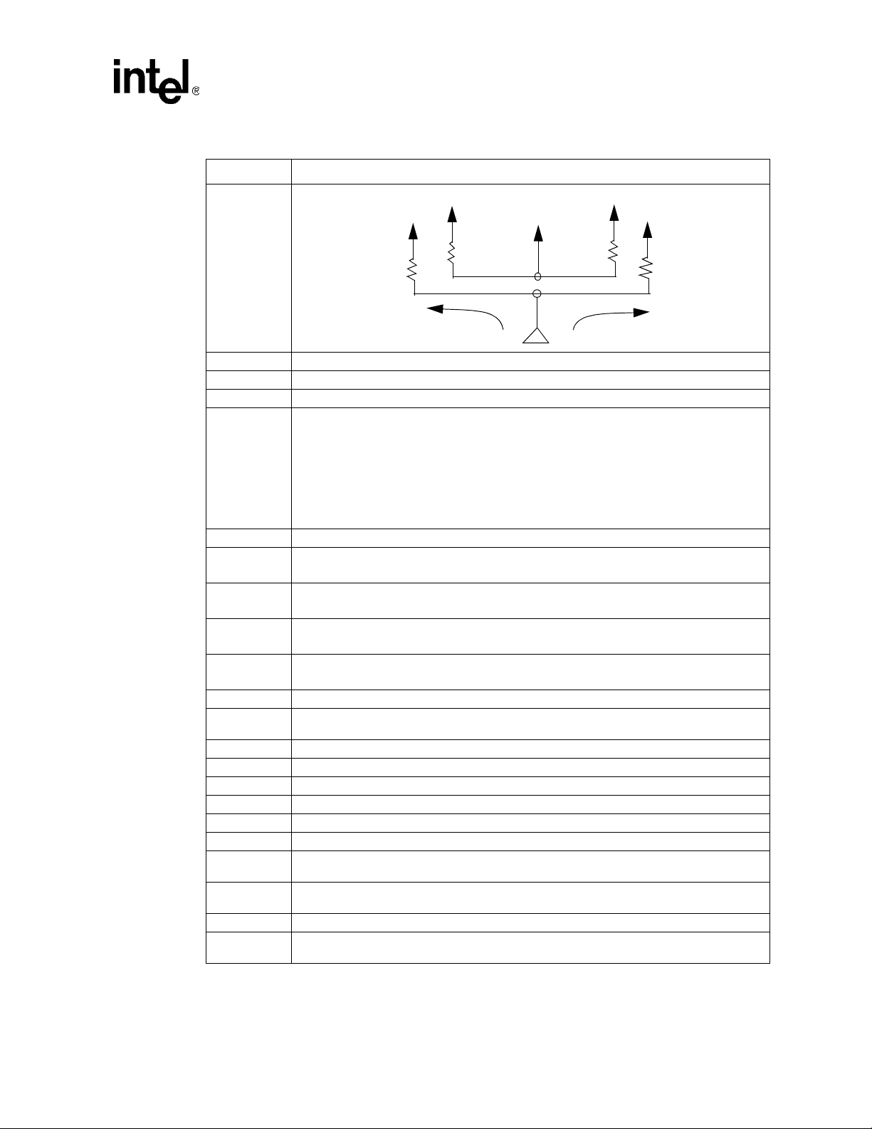
Table 1. Terminology and Definitions (Sheet 2 of 2)
Term Definition
A network that transmits a coupled signal to another network is aggressor network.
Intel® 80331 I/O Process or Design Guide
Introduction
Aggressor
Victim A network that receives a coupled cross-talk signal from anot her net wor k is a victi m network.
Network The trace of a PCB that completes an electrical connection between two or more components.
Stub Branch from a trunk terminating at the pad of an agent.
Intersymbol Interference (ISI). This occurs when a transition that has not been completely
dissipated, interferes with a signal being transmitted down a transmission line. ISI can impact
both the timing and signal integrity. It is dependent on frequency, time delay of the line and the
ISI
CRB Customer Reference Board
PC1600
PC2100
PC2700
PC3200
Downstream At or toward the Primary PCI interface from the Secondary PCI interface
Local memory
DWORD 32-bit data word.
Local bus
Outbound At or toward the PCI interface of the 80331 AT U from the Internal Bus.
Inbound At or toward the Internal Bus of the 80331 from the PCI interface of the ATU.
Local processor Intel XScale
Core processor Intel XScale® core within the 80331.
Flip Chip
Mode
Conversion
ROMB Raid on motherboard
ODT
refection coefficient at the driver and receiver. Examples of ISI patterns that could be used in
testing at the maximum allowable frequencies are the sequences shown below:
JEDEC Names for DDR based on peak data rates.
PC1600= clock of 100 MHz * 2 data words/clock * 8 bytes = 1600 MB/sec
JEDEC Names for DDR based on peak data rates.
PC2100= clock of 133 MHz * 2 data words/clock * 8 bytes = 2128 MB/sec
JEDEC Names for DDR II based on peak data rates.
PC2700= clock of 167 MHz * 2 data words/clock * 8 bytes = 2672 MB/sec
JEDEC Names for DDR II based on peak data rates.
PC3200= clock of 200 MHz * 2 data words/clock * 8 bytes = 3200 MB/sec
Memory subsystem on the Intel XScale
busses.
80331 Internal Bus.
FC-BGA (flip chip-ball grid array) chip packages are designed with core flipped up on the back of
the chip, facing away from the PCB. This allows more efficient cooling of the package.
Mode Conversions are due to imperfections on the interconnect which transform differential
mode voltage to common mode voltage and common mode voltage to differential voltage.
On Die Termination - eliminates the need for termination resistors by placing the termination at
the chip.
Zo
®
core within the 80331.
Zo
Victim Network
Aggressor Network
0101010101010101
0011001100110011
0001110001110001111
®
core DDR SDRAM or Peripheral Bus Interface
Zo
Zo
13
Page 14

Intel® 80331 I/O Process or Design Guide
Introduction
1.1.2 Other Relevant Documents
1. Intel® 80331 I/O Processor Specification Update (273930), Intel Corporation
2. Intel® 80331 I/O Processor Data sheet (273943), Intel Corporation
3. Intel® 80331 I/O Processor Developer’s Manual (273942), Intel Corporation
4. Intel XScale® 80200 Processor based on Intel® Microarchitecture Developer’s Manual
(273411), Intel Corp orati on
5. PCI Local Bus Specification, Revision 2.3 - PCI Special Interest Group
6. PCI-X Specification, Revision 1.0b - PCI Special Interest Group
7. PCI Bus Power Management Interface Specification, Revis ion 1.1 - PCI Special Interest
Group
8. IEEE Standard Test Access Port and Boundary-Scan Architecture (IEEE JTAG-1149.1-1990)
14
Page 15

Intel® 80331 I/O Process or Design Guide
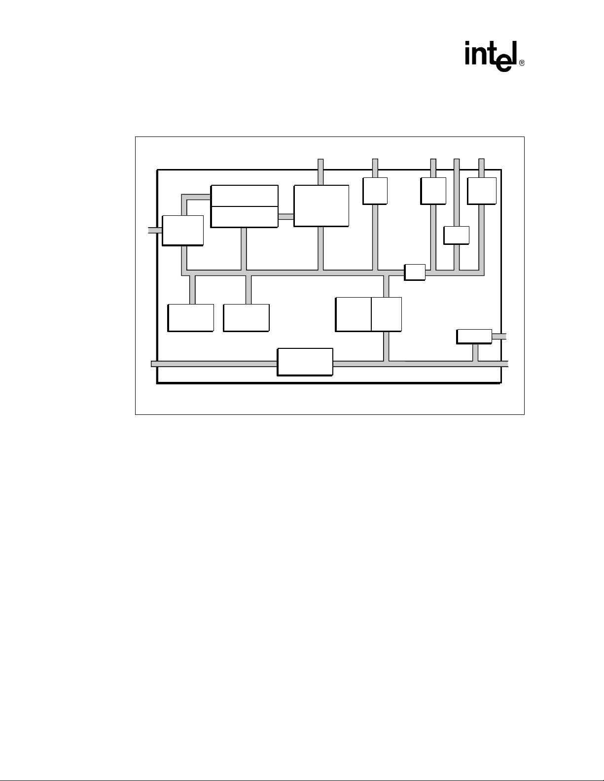
1.2 About the Intel® 80331 I/O Processor
The 80331 is a multi-function device that integrates the Intel XScale® core (ARM* architecture
compliant) with intelligent peripherals and PCI-to-PCI Bridge. The 80331 consolidates the
following into a single system:
• Intel XScale
• PCI-to-PCI Bridge supporting PCI-X interfaces on the Primary and Secondary bus.
• Address Translation Unit (PCI-to-Internal Bus Application Bridge) interfaced to the
Secondary Bus
• High-Performance Memory Controller
• Interrupt Controller with up to 13 external interrupt inputs
• Two Direct Memory Access (DMA) Controllers
• Application Accelerator
• Messaging Unit
• Peripheral Bus Interface Unit
• Performance Monitor
• Tw o I
®
core
2
C Bus Interface Units
Introduction
• Two 16550 compatible UARTs with flow control (four pins)
• Eight General Purpose Input Output (GPIO) ports
It is an integrated processor that addresses the needs of intelligent I/O applications and helps
reduce intelligent I/O system costs.
15
Page 16
Intel® 80331 I/O Process or Design Guide
Introduction
Figure 1 provides a block diagram of the 80331.
Figure 1. Intel® 80331 I/O Processor Functional Block Diagram
Message
Unit
16-bit
PBI
BRG
ATU
Intel® XScale™
Core
Bus Interface
Interrupt
Controller
& Timers
Application
Accelerator
Primary PCI Bus Secondary PCI Bus
Unit
Internal Bus
2 Channel
DMA
Controller
32/64-bit DDR
Interface
Memory
Controller
PCI-to-PCI
Bridge
UART
Units
2 - 1²C
Units
GPIO
Arbiter
B2472-01
16
Page 17

Intel® 80331 I/O Process or Design Guide
Package Information
Package Information 2
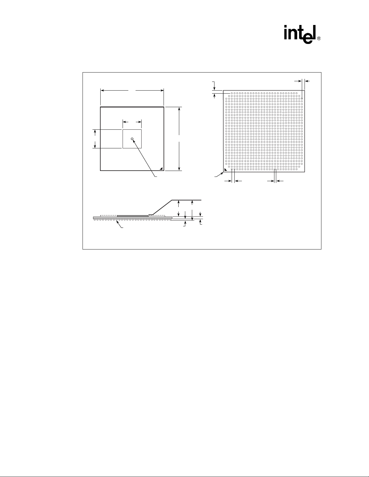
The 80331 is of fered in a Flip Chip Ball Grid Array (FCBGA) package. This is a fu ll-array package
with 829 ball connections. The mechanical dimensions for this package are provided in the figure
below and
(FCBGA), mapped by pin function. This diagram is helpfu l in placing components around the
80331 for the layout of a PCB. To simplify routing and minimize the number of cross traces, keep
this layout in mind when placi ng compo nents on y our board. Th e signals, by des ign, are located o n
the FCBGA package to simplify signal routing and system implementation.
Table 2. FC-style, H-PBGA Package Dimensions
Table 2. Figure 3 and Figure 4 show the 829 pins of the Flip Chip Ball Grid Array
829-Pin BGA
Symbol Minimum Maximum
A 2.392 2.942
A1 0.50 0.70
A3 0.742 0.872
b 0.61 Ref.
C 1.15 1.37
D 37.45 37.55
E 37.45 37.55
F1 9.88 Ref.
F2 10.16 Ref.
e 1.27 Ref.
S1 0.97 Ref.
S2 0.97 Ref.
NOTE: Measurement in millimeters.
17
Page 18
Intel® 80331 I/O Process or Design Guide
Package Information
Figure 2. Intel® 80331 I/O Processor 829-Ball FCBGA Package Diagram
F2
S1
E
F1
Die
D
Pin #1
Corner
AJ
AH
AG
AF
AE
AD
AC
AB
AA
Y
W
V
U
T
R
P
N
M
L
K
J
H
G
F
E
D
C
B
A
1234
5 6 7 8 9 10111213141516171819 20212223242526272829
e
Top View Bottom View
A
A3
Seating Plane
A1
C
Side View
S2
øb
B1230-03
18
Page 19

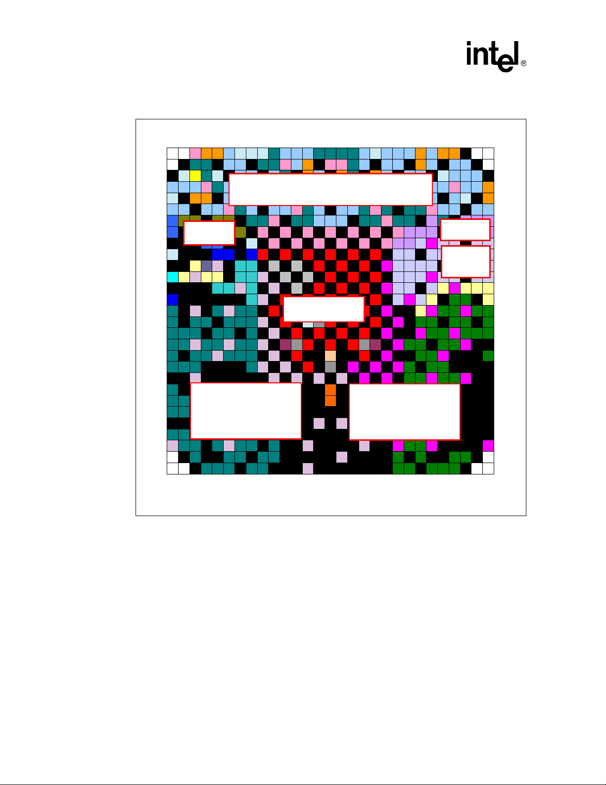
Intel® 80331 I/O Process or Design Guide
Figure 3. Intel® 80331 I/O Processor Preliminary Ballout (Top View)
Package Information
AJ
AH
AG
AF
AE
AD
AC
AB
AA
Y
W
V
U
T
R
P
N
M
L
K
J
H
G
F
E
D
C
B
A
GPIO
PBI
21
2223242526272829
DDR/DDRII/SDRAM
Secondary
PCI-X Bus
21
2223242526272829
VCC/VSS
JTAG
Primary
PCI-X Bus
1234567891011121314151617181920
AJ
AH
AG
AF
AE
AD
AC
AB
AA
Y
W
V
U
T
R
P
N
M
L
K
J
H
G
F
E
D
C
B
A
1234567891011121314151617181920
B1758-01
19
Page 20
Intel® 80331 I/O Process or Design Guide
Package Information
Figure 4. Intel® 80331 I/O Processor Preliminary Ballout (Bottom View)
1 2 3 4 5 6 7 8 9 10111213141516171819202122 23 24 25 26 27 28 29
AJ
AH
AG
AF
AE
AD
AC
AB
AA
Y
W
V
U
T
R
P
N
M
L
K
J
H
G
F
E
D
C
B
A
JTAG
Primary
PCI-X Bus
1 2 3 4 5 6 7 8 9 10111213 141516171819202122 23 24 25 26 27 28 29
DDRII/SDRAM
GPIO
VCC/VSS
Secondary
PCI-X Bus
PBI
AJ
AH
AG
AF
AE
AD
AC
AB
AA
Y
W
V
U
T
R
P
N
M
L
K
J
H
G
F
E
D
C
B
A
B1210-01
20
Page 21
Intel® 80331 I/O Process or Design Guide
1
2.1 Power Plane Layout
Figure 5 provides an example of how the 80331 DDR, CPU core and 1.5 V core power planes are
partitioned on the Intel® IQ80331 Evaluation Platform Board (IQ80331).
Note: The voltage for the secondary PCIX bus and primary PCIX bus can be on the same plane.
Figure 5. Intel® 80331 I/O Processor Power Plane Layout
VCC_DDR
Package Information
(Use Top Layer for VTT Plane)
DDR DIMM Connector
VCC_XSCALE
VCC 1.5 V
DDR VDD Regulator
To Regulators
B2529-0
21
Page 22
Intel® 80331 I/O Process or Design Guide
Package Information
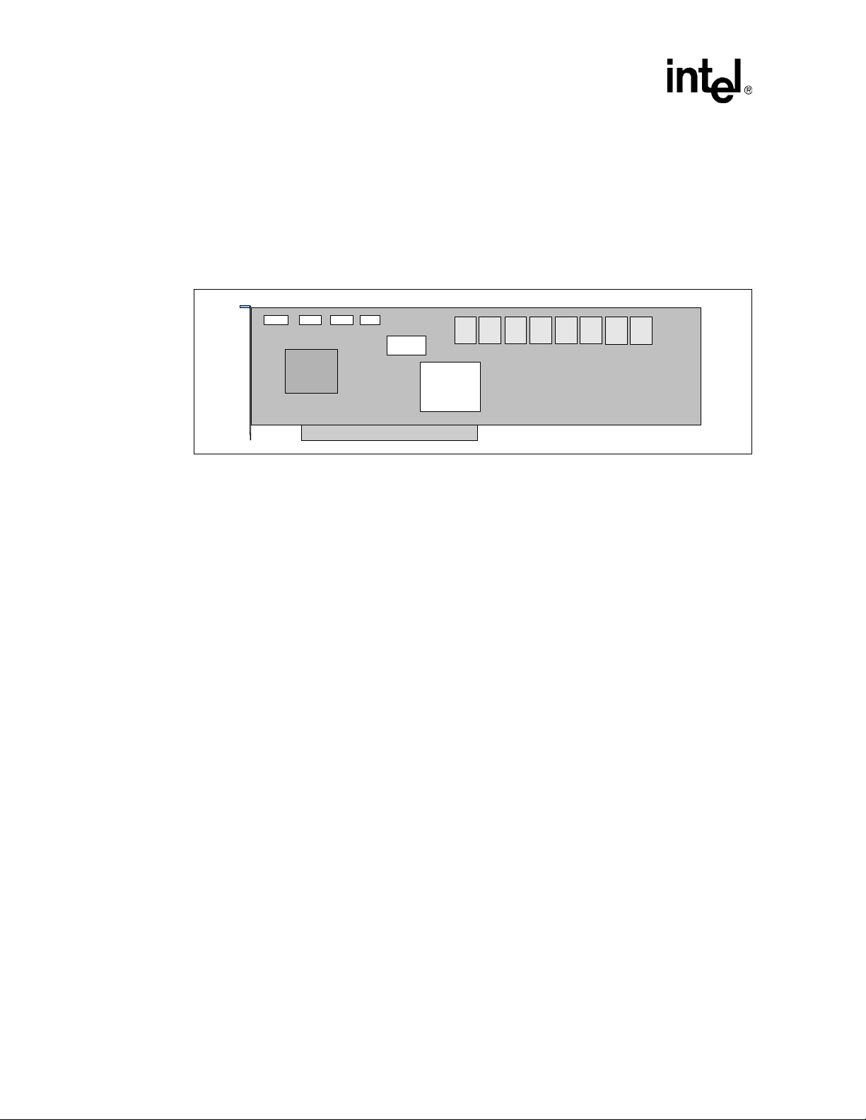
2.2 Intel® 80331 I/O Processor Applications
This section provides a block diagram of a 80331 Serial ATA adapter card application. This entire
SATA RAID card adapter can be implemented with just a few chips using the 80331 integrated
PCI-X bridge and IO processing capability.
Figure 6. Intel® 80331 I/O Processor PCI-X Adapter Card Block Diagram
SATA Connectors
SATA
Controller
4 Channel
Flash
PCI-X Edge
Intel® 80331
I/O Processor
DDR II
22
Page 23
Intel® 80331 I/O Process or Design Guide
Terminations
Terminations 3
This chapter provides the recommended pull-up and pull-down terminations for a 80331 layout.
Table 3 li sts these 80331 termination values. On a motherboard, the PCI Local Bus Specification,
Revision 2.3 requires that the PCI signals provide the termination resistors. Pull-ups on the PCI
signals are not required with PCIODT_EN = 1 (enabled), because they are implemented on the die.
Refer to the
Table 3. Terminations: Pull-up/Pull-down (Sheet 1 of 4)
Signal
PWRDELAY
Table 3 for more information.
Pull-up or Pull-down
Resistor Value (in Ohms)
If battery backup is
implemented:
• 1.5 K pull-up to 3.3 V is
required on
PWRDELAY.
Battery Backup not
implemented:
• This pin can be
permanently pulled low
with a 1.5K pull-down
Comments
NOTES:
• Alternatively tied to P_RST# refer to Section 11.4.2, “ARM
TRST# 1.5K pull-down*
TMS
TDI
TCK
GPIO[0]/U0_RXD 8.2 K pull-up Note : GPIO[7:0] initializes as inputs on assertion of P_RST#.
GPIO[1]/U0_TXD 8.2 K pull-up Note: GPIO[7:0] initializes as inputs on assertion of P_RST#.
GPIO[2]/U0_CTS# 8.2 K pull-up Note : GPIO[7:0] initializes as inputs on assertion of P_RST#.
GPIO[3]/U0_RTS# 8.2 K pull-up N ote: GPIO[7:0] initializes as inputs on assertion of P_RST#.
GPIO[4]/U1_RXD 8.2 K pull-up Note : GPIO[7:0] initializes as inputs on assertion of P_RST#.
GPIO[5]/U1_TXD 8.2 K pull-up Note: GPIO[7:0] initializes as inputs on assertion of P_RST#.
GPIO[6]/U1_CTS# 8.2 K pull-up Note : GPIO[7:0] initializes as inputs on assertion of P_RST#.
GPIO[7]/U1_RTS 8.2 K pull-up Note: GPIO[7:0] initializes as inputs on assertion of P_RST#.
ARB_EN (see comments)
NC when not being used
(has internal pull-up)
NC when not being used
(has internal pull-up)
1.5K pull-down when not
used
Multi-ICE” on page 142 for more information about using with a
ICE.
• When not used this signal is be tied to GND.
• This pin has an internal pull-up.
This signal has been defeatured. Please refer to the Intel® 80331
Specification Update for more information.
23
Page 24
Intel® 80331 I/O Process or Design Guide
Terminations
Table 3. Terminations: Pull-up/Pull-down (Sheet 2 of 4)
Signal
PCIODT_EN
P_32BITPCI#
S_INT[D:A]# . Refer to comments
S_LOCK# Refer to comments
S_SERR# Refer to comments
S_TRDY# Refer to comments
S_PERR# Refer to comments
S_DEVSEL# Refer to comments
S_FRAME# Refer to comments
S_STOP# Refer to comments
S_IRDY# Refer to comments
S_AD[63:32] Refer to comments
S_C/BE[7:4 ] Re fe r to c omments
S_PAR64 Refer to comments
S_REQ64# Re fer to comments
S_ACK64# Refer to comments
S_M66EN Refer to comments
Pull-up or Pull-down
Resistor Value (in Ohms)
1.5 K pull-down when
needed (see comments)
1.5 K pull-down when
needed (see comments)
PCI Bus ODT Enable: is latched on the rising (deasserting) edge of
P_RST#, and determines when the PCI-X interface has On Die
Termination enabled valid on the secondary PCI bus only.
• 0 = ODT disabled on the secondary PCI bus. (Requires pull-down
resistor).
• 1 = ODT enabled on the secondary PCI bus. (Default mode).
This signal controls termination for the following signals:
S_AD[63:32], S_C/BE[7:4]#, S_PAR64, S_REQ64#, S_REQ[3:0]#,
S_ACK64#, S_FRAME#, S_IRDY#, S_DEVSEL#, S_TRDY#,
S_STOP#, S_PERR#, S_LOCK#, S_M66EN, S_SERR# and
XINT[3:0]#
NOTE: This signal is muxed onto signal A[20].
Primary PCI-X Bus Width: By default, identifies 80331 subsystem as
64-bit unless user attaches appropriate pull-down resistor.
0 = 32 bit wide bus. (Requires pull-down resistor).
1 = 64 bit wide bus. (Default mode).
NOTE: Muxed onto signal A[2]
• When PCIODT_EN = 1 no external pull-up needed
• When PCIODT_EN = 0, then 8.2 K pull-up is required.
• When PCIODT_EN = 1 no external pull-up needed
• When PCIODT_EN = 0, then 8.2 K pull-up is required.
• When PCIODT_EN = 1 no external pull-up needed
• When PCIODT_EN = 0, then 8.2 K pull-up is required.
• When PCIODT_EN = 1 no external pull-up needed
• When PCIODT_EN = 0, then 8.2 K pull-up is required.
• When PCIODT_EN = 1 no external pull-up needed
• When PCIODT_EN = 0, then 8.2 K pull-up is required.
• When PCIODT_EN = 1 no external pull-up needed
• When PCIODT_EN = 0, then 8.2 K pull-up is required.
• When PCIODT_EN = 1 no external pull-up needed
• When PCIODT_EN = 0, then 8.2 K pull-up is required.
• When PCIODT_EN = 1 no external pull-up needed
• When PCIODT_EN = 0, then 8.2 K pull-up is required.
• When PCIODT_EN = 1 no external pull-up needed
• When PCIODT_EN = 0, then 8.2 K pull-up is required.
• When PCIODT_EN = 1 no external pull-up needed
• When PCIODT_EN = 0, then 8.2 K pull-up is required.
• When PCIODT_EN = 1 no external pull-up needed
• When PCIODT_EN = 0, then 8.2 K pull-up is required.
• When PCIODT_EN = 1 no external pull-up needed
• When PCIODT_EN = 0, then 8.2 K pull-up is required.
• When PCIODT_EN = 1 no external pull-up needed
• When PCIODT_EN = 0, then 8.2 K pull-up is required.
• When PCIODT_EN = 1 no external pull-up needed
• When PCIODT_EN = 0, then 8.2 K pull-up is required.
• When PCIODT_EN = 1 no external pull-up needed
• When PCIODT_EN = 0, then 8.2 K pull-up is required when PCI
bus is to operate at 66 MHz. This signal is grounded for 33 MHz
operation.
Comments
24
Page 25
Intel® 80331 I/O Process or Design Guide
Table 3. Terminations: Pull-up/Pull-down (Sheet 3 of 4)
Signal
S_RCOMP 100 ohm +/- 1% to GND
SCLKIN
S_REQ[3:0]# Refer to comments
S_PCIXCAP Refer to comments
PRIVMEM
PRIVDEV 1.5 K pull-down when
P_RCOMP 100 ohm +/- 1% to GND
P_REQ# Refer to comments
P_LOCK# Refer to comments
P_SERR# Refer to comments
P_TRDY# Refer to comments
P_PERR# Refer to comments
P_DEVSEL# Refer to comments
P_FRAME# Refer to comments
P_STOP# Refer to comments
P_IRDY# Refer to comments
P_AD[63:32] Refer to comments
P_C/BE[7:4] Refer to comments
P_PAR64 Refer to comments
P_REQ64# Refer to comments
P_ACK64# Refer to comments
Pull-up or Pull-down
Resistor Value (in Ohms)
Through 33.2ohm resistor
to S_CLKOUT
1.5 K pull-down when
needed (refer to comments)
needed (refer to comments)
• When PCIODT_EN = 1 no external pull-up needed
• When PCIODT_EN = 0, then 8.2 K pull-up is required.
66 MHz PCI: connect pin to GND.
66 MHz PCI-X: use 0.01 µF to GND || 10 K resistor to GND.
100 MHz PCI-X: use 0.01 µF to GND.
133 MHz PCI-X: use 0.01 µF to GND.
Private Memory Enable: PRIVMEM latched at rising (deasserting)
edge of P_RST# and determines when the 80331 operates with
Private Memory Space on the secondary PCI bus of the PCI-to-PCI
Bridge.
0 = Normal addressing mode. Requires pull-down resistor.
1 = Private Addressing enable in PCI-to-PCI Bridge. (Default mode)
Muxed onto signal A[1],
Private Device Enable: PRIVDEV latched at rising (deasserting)
edge of P_RST# and determines when the 80331 operates with
Private Device enabled on the secondary PCI bus of the PCI-to-PCI
Bridge.
0 = All Secondary PCI devices are accessible to Primary PCI
configuration cycles. (Requires pull-down resistor).
1 = Private Devices enabled in PCI-to-PCI Bridge. (Default mode)
Muxed onto signal A[0]
8.2 K pull-up is required when not already pulled up on the PCI bus.
An add-in card may rely on the motherboard to pull-up this signal.
8.2 K pull-up is required when not already pulled up on the PCI bus.
An add-in card may rely on the motherboard to pull-up this signal.
8.2 K pull-up is required when not already pulled up on the PCI bus.
An add-in card may rely on the motherboard to pull-up this signal.
8.2 K pull-up is required when not already pulled up on the PCI bus.
An add-in card may rely on the motherboard to pull-up this signal.
8.2 K pull-up is required when not already pulled up on the PCI bus.
An add-in card may rely on the motherboard to pull-up this signal.
8.2 K pull-up is required when not already pulled up on the PCI bus.
An add-in card may rely on the motherboard to pull-up this signal.
8.2 K pull-up is required when not already pulled up on the PCI bus.
An add-in card may rely on the motherboard to pull-up this signal.
8.2 K pull-up is required when not already pulled up on the PCI bus.
An add-in card may rely on the motherboard to pull-up this signal.
8.2 K pull-up is required when not already pulled up on the PCI bus.
An add-in card may rely on the motherboard to pull-up this signal.
8.2 K pull-up is required when not already pulled up on the PCI bus.
An add-in card may rely on the motherboard to pull-up this signal.
8.2 K pull-up is required when not already pulled up on the PCI bus.
An add-in card may rely on the motherboard to pull-up this signal.
8.2 K pull-up is required when not already pulled up on the PCI bus.
An add-in card may rely on the motherboard to pull-up this signal.
8.2 K pull-up is required when not already pulled up on the PCI bus.
An add-in card may rely on the motherboard to pull-up this signal.
8.2 K pull-up is required when not already pulled up on the PCI bus.
An add-in card may rely on the motherboard to pull-up this signal.
Terminations
Comments
1
25
Page 26
Intel® 80331 I/O Process or Design Guide
Terminations
Table 3. Terminations: Pull-up/Pull-down (Sheet 4 of 4)
Signal
P_M66EN Refer to comments
P_REQ# Refer to comments
M_CK[2:0], M_CK[2:0]# Refer to comments For M_CKs and M_CK#s not used leave these pins unconnected.
DQS[8:0]# Refer to Comments When not in DDRII mode these signals are NC’s
DDRRES[2:1]
HPI# 8.2 K pull-up
P_BOOT16#
MEM_TYPE
RETRY
CORE_RST#
BRG_EN
DDRSLWCRES Refer to Figure 9
DDRIMPCRES Refer to Figure 9
ODT[1:0]
Pull-up or Pull-down
Resistor Value (in Ohms)
•Refer to Figure 8 for the
recommended
termination for DDRII
mode.
• When not in DDRII
mode these signals
have a 1.0 K pull-down.
1.5 K pull-down when
needed (refer to comments)
1.5 K pull-down when
needed (refer to comments)
1.5 K pull-down when
needed (refer to comments)
1.5 K pull-down when
needed (refer to comments)
1.5 K pull-down when
needed (refer to comments)
Connect to ODT on DIMM
terminated with 49.9 ohm
resistor to VTT
Comments
8.2 K pull-up is required when not already pulled up on the PCI bus.
An add-in card may rely on the motherboard to pull-up this signal.
8.2 K pull-up is required when not already pulled up on the PCI bus.
An add-in card may rely on the motherboard to pull-up this signal.
Bus Width is latched on the rising (asserting) edge of P_RST#, it sets
the default bus width for the PBI Memory Boot window:
• 0 = 16 bits wide (Requires a pull-down resistor.)
• 1 = 8 bits wide (Default mode)
Muxed onto signal AD[4].
Memory Type: MEM_TYPE is latched on the rising (asserting) edge
of P_RST# and it defines the speed of the DDR SDRAM interface.
0 = DDR-II SDRAM at 400 MHz (Required pull-down resistor.)
1 = DDR SDRAM at 333 MHz (Default mode)
Muxed onto signal AD[2]
Configuration Retry Mode: RETRY is lat ched on t he rising (asserting)
edge of P_RST# and determines when PCI interface of the ATU
disables PCI configuration cycles by signaling a retry until the
configuration cycle retry bit is cleared in the PCI configuration and
status register.
0 = Configuration Cycles enabled (Requires pull down resistor.)
1 = Configuration Retry enabled in the ATU and the Configuration.
(Default mode)
Muxed onto signal AD[6]
Core Reset Mode is latched on the rising (asserting) edge of P_RST#
and determines when the Intel
processor reset bit is cleared in PCI configuration and status register.
0 = Hold in reset. (Requires pull-down resistor.)
1 = Do not hold in reset. (Default mode)
Muxed onto signal AD[5]
Bridge Enable: BRG_EN latched at rising (deasserting) edge of
P_RST# and determines when the 80331 operates wi th PCI- to-PCI
Bridge.
0 = Disable Bridge, enable P_CLK input on S_CLKIN input.
(Requires pull-down resistor)
1 = Enabled Bridge. (Default mode)
Muxed onto signal AD[0]
When not used this pin is left as a “no connect”.
®
XScale™ core is held in reset until the
26
Page 27

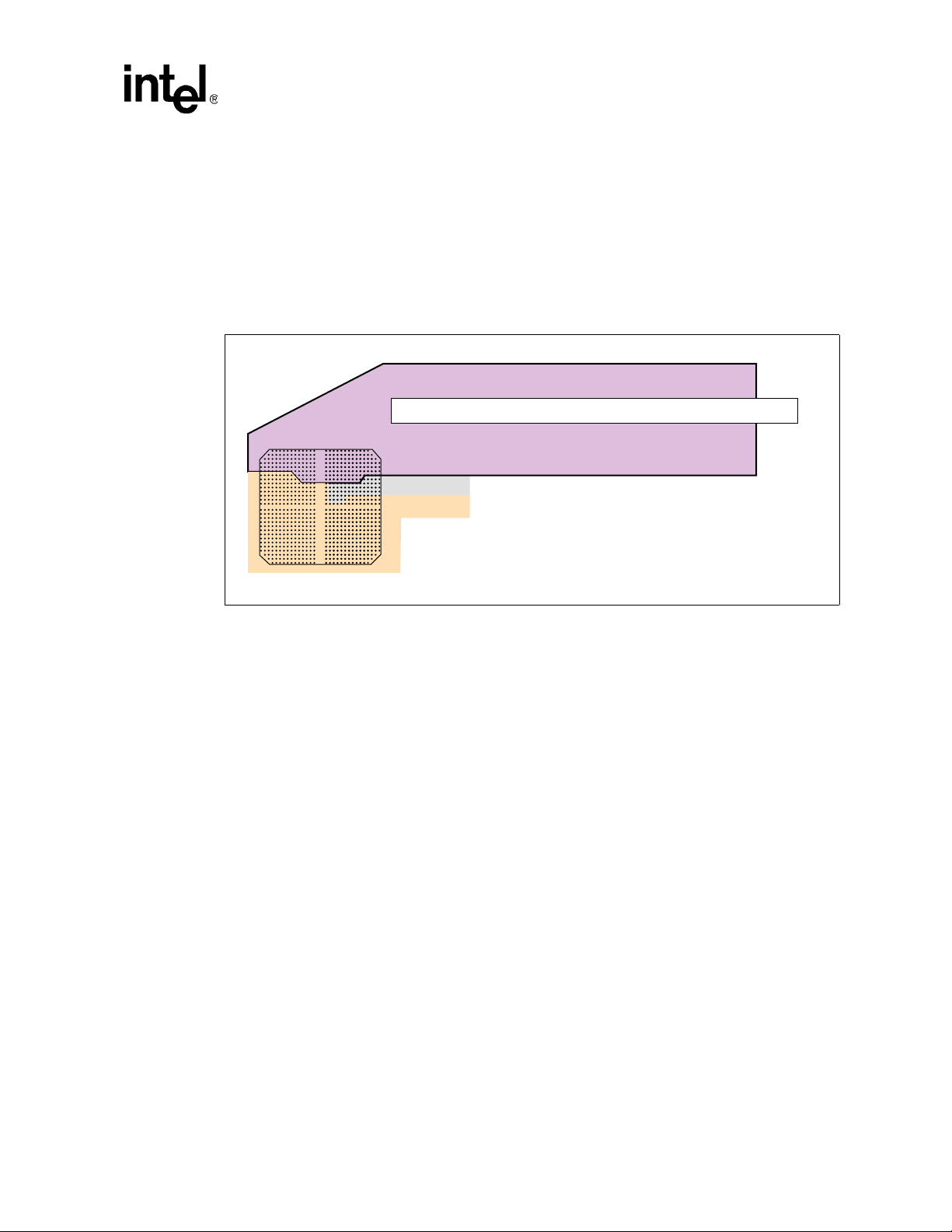
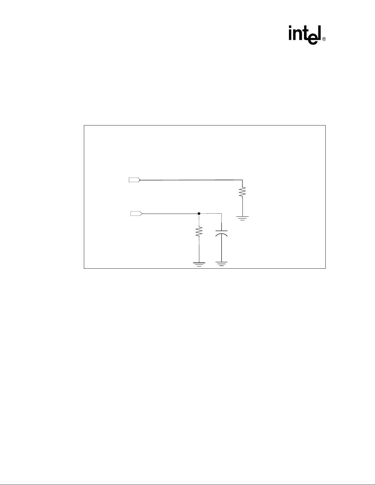
3.1 Analog Filters
The following section describes filters needed for biasing PLL circuitry.
Intel® 80331 I/O Process or Design Guide
Terminations
3.1.1 V
T o reduce clock skew, the V
package. The lowpass filter, as shown in
timing relationships in system designs. The node con necti ng V
short as possible. The
- V
The following notes list the layout guidelines for this filter.
Figure 7. V
CCPLL
Pin Requirements
balls for the Phase Lock Loop (PLL) circuit are isolated on the
CCPLL
Figure 7 reduces noise induced clock jitter and its effects on
and the capacitor must be as
CCPLL
Figure 7 filter circuit is recommended for each of the Four PLL pairs: V
SSA1, VCCPLL2
- V
SSA2, VCCPLL4
- V
SSA4
and V
CCPLL5
- V
SSA5
pairs.
• 4.7 µH (Inductor)
— L must be magnetically shielded
—ESR: max < 0.4Ω
— rated at 45mA
— An example of this inductor is TDK part number MLZ2012E4R7P.
• 22 µF (Capacitor)
—ESR: max < 0.4Ω
— ESL < 3.0nH
— Place 22 µF capacitor as close as possible to package pin.
• 0.5 ohm 1% (Resistor)
— 1/16W 6.3V
• 0.5 ohm 1% resistor must be placed between V
• Route V
• V
CCPLL
[1-5] and V
CCPLL
[1-5] and V
[1-5] as differential traces.
SSA
[1-5] traces must be ground referenced (No VCC references).
SSA
and L. The resistor rating is 1/16W.
CC
• Maximum total board trace length = 1.2”.
• Minimum trace space to other nets = 30 mils.
• The 1.5 V supply regulator used for the PLL filter must have less than +/- 3% tolerance.
• Note: V
Configuration
CCPLL
SSA1
, V
SSA2, VSSA4 and VSSA5
pins must not be connected to ground.
CCPLL1
1.5 V
0.5 ohms , 1%
Note: Do Not conn ect V SSA pins to g round
Board Trace:
Trace w idth > 25 mils
Trace Spac ing < 10 mils
Trace Length < 600 mils
4.7 uH <25%
22 uF <20%
Board Route
Traces
Breakout Traces
Beneath BGA
Breakout Trace:
Trace w idth > 6 mils
Tra c e S pa c in g < 6 mils
Trace Length < 600 mils
VCCPLL
Intel®
I/O Processor
VSSA
27
Page 28
Intel® 80331 I/O Process or Design Guide
Terminations
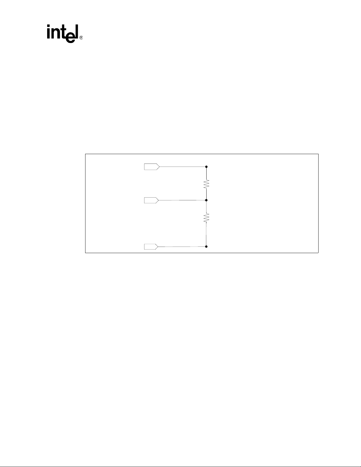
3.2 DDR Resistor Compensation
The Figure 8 provides the 80331 DDR II DDRES circuitry. The DDRRES1 resistor has a tight
toleranc e of 40.2 ohm 0.5%. DDRRES2 is used as compensation for DDR-II OCD. Due to the fact that
OCD is not supported this pin should be pulled to GND with a 1K resistor.
s
Note: when not in DDR II mode these pins must have a 1.0 K pull-down to GND.
Figure 8. Intel® 80331 I/O Processor DDRRES Resistor Compensation Circuitry
DDRRES2
1K ohms
DDRRES1
40.2 ohms
0.5%
0.1uF
28
Page 29
3.3 DDR Driver Compensation
External reference resistors are used to control slew rate and driver impedance. The
DDRIMPCRES (or DDRDRVCRES) resistor directly controls the on-die termination (ODT). The
recommendations are as follows:
• DDRIMPCRES: controls on-die termination, DDR - 385 ohms, DDRII - 285 ohms. Note that
the closest standard 1% resistors are acceptable
• DDRSLWRCRES: controls slew rate and driver impedance, DDR 845 ohms, DDRII
ohms.
825
With these values the ODT is 150/75 ohms for DDRII and 200/100 ohms for DDR.
Figure 9. DDR Driver Compensation Circuitry
DDRIMPCRES
DDRCRES0
Intel® 80331 I/O Process or Design Guide
Terminations
.
385 ohms DDR
285 ohms DDRII
DDRSLWCRES
845 ohms DDR
825 ohms DDRII
29
Page 30

Intel® 80331 I/O Process or Design Guide
Terminations
This Page Intentionally Left Blank
30
Page 31

Intel® 80331 I/O Process or Design Guide
Routing Guidelines
Routing Guidelines 4
This chapter provides some basic ro uting guidel ines for layout and design of a printed circuit board
80331. The high-speed clocking required when designing with the 80331 requires special
using
attention to signal integrity. In fact, it is highly recommended that the board design be simulated to
determine optimum layout for signal integrity. The information in this chapter provides guidelines
to aid the designer with board layout. Several factors influence the signal integrity of a
design. These factors include:
• Power distribution
• Minimizing crosstalk
• Decoupling
• Layout considerations when routing the DDR memory, DDR II memory, and PCI-X bus
interfaces
80331
4.1 General Routing Guidelines
This section details general routing guidelines for designing with 80331. The order in which
signals are routed varies from designer to designer. Some designers prefer to route all clock signals
first, while others pre fer to route al l high -speed b us sig nals fi rst. Ei ther ord er can be u sed, pr ovide d
the guidelines listed here are followed.
31
Page 32

Intel® 80331 I/O Process or Design Guide
Routing Guidelines
4.2 Crosstalk
Crosstalk is caused by capacitive and inductive cou pling between si gnals. Crosstal k is composed of
both backward and forward crosstalk components. Backward crosstalk creates an induced signal on
victim network that propagates in the opposite direction of the aggressor signal. Forward crosstalk
creates a signal that propagates in the same direction as the aggressor signal.
Circuit board analysis software is used to analyze your board layout for crosstalk probl ems. Examples
of 2D analysis tools include Parasitic Parameters from ANSOFT
Crosstalk problems occur when circuit etch lines run in parallel. When board analysis software is not
available, the layout needs to be designed to mai ntain at least the minimum recommended spacing for
bus interfaces.
• A general guideline to use is, that space distance between adjacent signals be a least 3.3 times
the distance from signal trace to the nearest return plane. The coupled noise between adjacent
traces decreases by the square of the distance between the adjacent traces.
• It is also recommended to specify the height of the above reference plane when laying out
traces and provide this parameter to the PCB manufacturer. By moving traces closer to the
nearest reference plane, the coupled noise decreases by the square of the distance to the
reference plane.
Figure 10. Crosstalk Effects on Trace Distance and Height
P
H
aggressor victim
Reference Plane
• Avoid slots in the ground plane. Slots increases mutual inductance thus increasing crosstalk.
• Throughout the design guide unbroken GND reference planes are recommended. If it is not
possible to route over an unbroken ground plane then an unbroken power plane is acceptable.
If it is necessary to use power plane referencing, it is better to reference the power plane used
by the I/O connector (if applicable). It is also recommended to add decoup ling to the connector
near the pins.
*
and XFS from Quad Design*.
Reduce Crosstalk:
- Maximize P
- Minimize H
A9259-01
• Make sure that ground plane surrounding connector pin fields are not completely cleared out.
When this area is completely cleared out, around the connector pins, all the return current must
flow together around the pin field increasing crosstalk. The preferred method of laying out a
connector in the GND layer is shown in
32
Figure 11B.
Page 33

Figure 11. PCB Ground Layout Around Connectors
Connector
Connector Pins
GND PCB Layer
A. Incorrect method B. Correct method
Intel® 80331 I/O Process or Design Guide
Routing Guidelines
A9260-01
33
Page 34

Intel® 80331 I/O Process or Design Guide
Routing Guidelines
4.3 EMI Considerations
It is highl y recommended that good EMI design practices be followed when designing wit h the
80331.
• To minimize EMI on your PCB a useful technique is to not extend the power planes to the
edge of the board.
• Another technique is to surround the perimeter of your PCB layers with a GND trace. This
helps to shield the PCB with grounds minimizing radiation.
The below link can provide some useful general EMI guidelines considerations:
http://developer.intel.com/design/auto/mcs96/applnots/272673.htm
4.4 Power Distribution and Decoupling
Have ample decoupling to ground, for the power planes, to minimize the effects of the switching
currents. Three types of decoupling are: the bulk, the high-frequency ceramic, and the inter-plane
capacitors.
• Bulk capacitance consist of electrolytic or tantalum capacitors. These capacitors supply large
reservoirs of charge, but they are useful only at lower frequencies due to lead inductance
effects. The bulk capacitors can be located anywhere on the board.
• For fast switching currents, high-frequency low-inductance capacitors are most effective.
Place these capacitors as close to the device being decoupled as possible. This minimizes the
parasitic resistance and inductance associated with board traces and vias.
• Use an inter-plane capacitor between power and ground planes to reduce the effective plane
impedance at high frequencies. The general guideline for placing capacitors is to place
high-frequency ceramic capacitors as close as possible to the module.
4.4.1 D ecoupling
Inadequate high-frequency decoupling results in intermittent and unreliable behavior.
A general guideline recommends that you use the largest easily available capacitor in the lowest
inductance package. The high speed decoupling capacitor should be placed as close to the pin as
possible with short, wide trace.
Table 4 provides the details on the recommended decoupling capacitors for each of the voltage
planes.
Table 4. Decoupling Recommendations
Volta ge Plan e Voltage Pins Package C (µF)
Number of
Caps
PCI/PCI-X 3.3V VCC33 1210 22 3
PCI/PCI-X 3.3V VCC33 0603 0.1 12
PCI/PCI-X 3.3V VCC33 7343 150 1
DDR/DDRII 2.5/1.8V VCC25/18 0603 0.1 14
34
Page 35

Table 4. Decoupling Recommendations
Intel® 80331 I/O Process or Design Guide
Routing Guidelines
Voltage Plane Voltage Pins Package C (µF)
DDR/DDRII 2.5/1.8V VCC25/18 1210 22 2
DDR/DDRII 2.5/1.8V VCC25/18 7343 150 1
Core 1.5V VCC15 0603 0.1 17
Core 1.5V VCC15 1210 22 2
CPU 1.35V VCC13 0603 0.1 6
CPU 1.35V VCC13 1206 10 1
CPU 1.35V VCC13 1210 22 1
NOTES:
1. Polymerized organic capacitors recommended for bulk decoupling.
2. X5R, X7R or COG dielectric recommended for ceramic capacitors.
Number of
Caps
35
Page 36

Intel® 80331 I/O Process or Design Guide
Routing Guidelines
4.5 Trace Impedance
All signal layers require controlled impedance of 50 Ω +/- 15%, microstrip or stripline where
appropriate for motherboard applicati ons and 60
applications. Selecting the appropriate board stack-up to minimize impedance variations is very
important. When calculating flight times, it is important to consider the minimum and maximum
trace impedance based on the switching neighboring traces. Use wider spaces between traces , since
this can minimize trace-to-trace coupling, and reduce cross talk.
When a different stack up is used the trace widths must be adjusted appropriately. When wider
traces are used, the trace spacing must be adjusted accordingly (linearly).
It is highly recommended that a 2D Field Solver be used to design the high-speed traces. The
following Impedance Calculator URL provide approximations for the trace impedance of various
topologies. They may be used t o generate the starting point for a full 2D Field solver.
http://emclab.umr.edu/pcbtlc/
The following website link provides a useful basic guideline for calculating trace parameters:
http://www.ultracad.com/calc.htm
Ω +/- 15%, microstrip or stripline, for add- in card
Note: Using stripline transmission lines may give better results than m icrost rip. This is due to th e
difficulty of precisely controlling the dielectric constant of the solder mask, and the difficulty in
limiting the plated thickness of microstrip conductors, which can substantially increase cross-talk.
36
Page 37

Intel® 80331 I/O Process or Design Guide
Board Layout Guidelines
Board Layout Guidelines 5
This section provides details on the motherboard and adapter card stackup suggestions. It is highly
recommended that signal integrity simulations be run to verify each 80331 PCB layout especially
when it deviates from the recommendations listed in these design guidelines. The information in
this chapter is an example of a stackup for a motherboard and an adapter card which can be used as
a reference.
5.1 Motherboard Stack Up Information
When 80331 is used in server and workstation Raid On Mother Board (ROMB) appli cations the
motherboard is implemented on eight layers. The specified impedance range for all board
implementations are 50 ohms +/-15%. Adjustments are made for interfaces specified at other
impedances.
The motherboard is supporting other components in addit io n to 8033 1, so i t is ass umed that
server/workstation motherboard requirements dominates to assu re the proc essor and memory
subsystem can be implemented with typical 50-ohm guidelines. Dimensions and tolerances for t he
motherboard are per
Table 5 defines the typical layer geometries for six or eight layer boards.
Table 5. Refer to Figure 12 for location of variables in Table 5.
T a ble 5. Motherboard Stack Up, Stripline and Microstrip (Sheet 1 of 2)
Variable Type
Solder Mask
Thickness (mil)
Core Thickness (mil) N/A 9.8 9.6 10
Core E
Plane Thickness
Trace Height
Trace Thickness
Trace Width (mil) Microstrip 5.0 3.5 6.5
(mil)
(mil)
Preg E
(mil)
N/A 0.8 0.6 1.0
N/A 3.653.653.65
r
N/A 4.30 3.75 4.85 2113 material.
r
Power 2.7 2.5 2.9
Ground 1.35 1.15 1.55
13.53.33.7
23.53.33.7
3 10.5 9.9 11.1
Microstrip 4.30 3.75 4.85 2113 material.
Stripline1 4.30 3.75 4.85 2113 material.
r
Stripline2 4.66 4.19 5.13
Microstrip 1.75 1.2 2.3
Stripline 1.4 1.2 1.6
Nominal
(mils)
Minimum
(mils)
Maximum
(mils)
The trace height is determined to achieve a nominal
50 ohms.Solder Mask E
7628 material. Trace height 3 is composed of one
piece of 2113 and one piece of 7628. It is assumed
that the 7628 material covers the bottom and sides
of the layer 3 traces as well as the top and sides of
the layer 4 traces. The 2113 material covers the top
of the layer three traces and the bottom of the layer
4 traces.
Notes
37
Page 38

Intel® 80331 I/O Process or Design Guide
Board Layout Guidelines
Table 5. Motherboard Stack Up, Stripline and Microstrip (Sheet 2 of 2)
Variable Type
Nominal
(mils)
Minimum
(mils)
Maximum
(mils)
Stripline 4.0 2.5 5.5
Microstrip 15.0 - - Each interface sets the trace spacing based on its
Trace Spaci ng (mil)
Stripline 12.0 - -
Total Thickness (mil) FR4 62.0 56.0 68.0
Trace V el ocity (ps/in)
Trace Impedance
(ohms)
Microstrip - 135 141
Stripline 167 178
Microstrip 50 42.5 57.5
Stripline 50 45 55
NOTE: Each interface sets the trace spacing based on its signal integrity of differential impedance
requirements. For the purposes of the building the transmission line models, it is assumed the artwork is
very accurate and therefore a constant. Thus, all the variability in the trace spacing is the result of the
tolerances of the trace width.
Figure 12. Motherboard Stackup Recommendations
Notes
signal integrity of differential impedance
requirements. For the purposes of the building the
transmission line models, it is assumed the artwork
is very accurate and therefore a constant. Thus, all
the variability in the trace spacing is the result of the
tolerances of the trace width.
Velocity varies based on variation in Er . It cannot be
controlled during the fab process.
Microstrip
Trace Spacing
L1
L2 (GND)
L3
L4 (VCC)
L5 (VCC)
Total Thickenss
L6
L7 (GN D )
Trace Spacing
Trace Width
L8
S tr ip lin e
Microstrip
L1
L3
Stripline
Trace Width
Microstrip Trace Thickness
Solder M ask Thickness
Trace Height 1
Trace Height 2
Stripline Trace Thickness
Trace Height 3
Core Thickness
Plane Thickness
L6
B3555-01
38
Page 39

Intel® 80331 I/O Process or Design Guide
5.2 Adapter Card Stackup
The 80331 can be implemented on PCI-X adapter cards with six or eight layer stackups. The
specified impedance range for all adapter card implementations are 60ohms +/-15%. Adjustments
are made for interfaces specified at other impedances.
for six or eight layer boards.
Note: Values are the same as the motherboard stack up with the exception of the impedance.
T a ble 6. Adapter Card Stack Up, Microstrip and Stripline
Table 6 defines the typical layer geometries
Board Layout Guidelines
Variable Type
Solder Mask Thickness (mil) N/A 0.8 0.6 1.0
Solder Mask E
Core Thickness (mil) N/A 2.8 3.0 3.2
Core E
Plane Thickness (mil)
Trace Height
Trace Thickness (mil)
Trace Width (mil) Microstrip 4.0 2.5 5.5
Total Thickne ss (mil) FR4 62.0 56.0 68.0
(mil)
Preg E
N/A 3.65 3.65 3.65
r
N/A 4.3 3.75 4.85 2113 material
r
Power 2.7 2.5 2.9
Ground 1.35 1.15 1.55
13.53.33.7
23.53.33.7
3 10.5 9.9 11.1
Microstrip 4.30 3.75 4.85 2113 material
Stripline1 4.30 3.75 4.85 2113 material
r
Stripline2 4.3 3.75 4.85
Microstrip 1.75 1.2 2.3
Stripline 1.4 1.2 1.6
Stripline 4.0 2.5 5.5
Nominal
(mils)
Minimum
(mils)
Maximum
(mils)
Notes
The trace height is determined to achieve a
nominal 60 ohms.
7628 material. Trace height 3 is composed
of one piece of 2113 and one piece of
7628.
Trace Spacing (using
microstrip E2E/C2C)
Trace Spacing (using
stripline E2E/C2C) [12]/[16]
Trace Impedance
NOTE: Each interface sets the trace spacing based on its signal integrity of differential impedance
requirements. For the purposes of the building the transmission line models, it is assumed the artwork is
very accurate and therefore a constant. Thus, all the variability in the trace spacing is the result of the
tolerances of the trace width.
[12]/[16]
Microstrip 60 51 69
Stripline 60 51 69
39
Page 40

Intel® 80331 I/O Process or Design Guide
Board Layout Guidelines
Figure 13. Adapter Card Stackup
Microstrip
Trace Spacing
L1
L3
Total Thickenss
L6
Microstrip
Trace Width
L2 (GND)
L4 (VCC)
L5 (VCC)
L7 (GND)
L8
Stripline
Trace Spacing
L1
L3
L6
Stripline
Trace Width
Microstrip Trace Thickness
Solder Mask Thickness
Trace Height 1
Trace Height 2
Stripline Trace Thickness
Trace Height 3
Core Thickness
Plane Thickness
B3555-01
40
Page 41

Intel® 80331 I/O Process or Design Guide
PCI-X Layout Guidelines
PCI-X Layout Guidelines 6
This chapter describes several factors to be co nsidered with a PCI/PCI-X design. These in clude the
PCI IDSEL, PCI RCOMP, PCI Interrupts, and PCI arbitration.
6.1 Interrupt Routing and IDSEL Lines
Figure 14 shows the 80331 connected to three PCI connectors. Notice that the interrupts are rotated
for each connector. The practice of Rotating INTs can also be used when connecting to individual
multifunction PCI devices as well. The IDSEL lines acts as chip selects during the configuration
cycles. Configuration cycles allow read and write access to one of the device configuration space
registers. The IDSEL lines can be mapped to upper address lines which are unused during the
configuration cycles. The ATU is hardwired to AD30 for IDSEL. Note that AD16 typically is
reserved for a PCI/PCI-X bridge. Each IDSEL line needs a 200
in the figure below.
ohm series resistor on it as shown
Figure 14. Interrupt and IDSEL Mapping
S_INT[D:A]#
S_AD[31:0]
®
Intel
80331 I/O
Processor
Note: PCI Bus Interrupt Signals “Rotate” on Subsequent PCI Connectors.
PCI Connector 1
INTA#
INTB#
INTC#
INTD#
200
AD20
Ω
INTA#
INTB#
INTC#
INTD#
IDSEL
PCI Connector 2 PCI Connector 3
INTB#
INTC#
INTD#
INTA#
AD17
200
Ω
INTA#
INTB#
INTC#
INTD#
IDSEL
INTC#
INTD#
INTA#
INTB#
AD18
200
INTA#
INTB#
INTC#
INTD#
IDSEL
Ω
41
Page 42

Intel® 80331 I/O Process or Design Guide
PCI-X Layout Guidelines
6.1.1 PCI Arbitration
80331 contains two PCI Arbiters to facilitate arbitration on the primary and secondary PCI buses.
Refer to the PCI Local Bus Specification, Revision 2.3, for more information on arbiter
algorithms. The specification essentially states that the algorithm needs to be fair to prevent any
one device from consuming to much of the PCI bandwidth.
A typical implementation of the arbitration logic is a two-level rotating round robin configuration.
A high priority status is assigned to a master request in level one and a low-level priority statu s is
assigned to a master request in level two. The arbiter checks each of the REQ# lines in the first
level. When none are asserted it traverses to checking level two. Once the GNT# has been asserted
to a master, this master has the lowest priority in its level.
The arbiter also conducts bus parking by driving A/D, C/BE# and PAR lines to a known value while
the bus is idle. The arbiter typically leaves the GNT# asserted to the master that used the bus last.
6.1.2 PCI Resistor Compensation
Figure 15 provides the recommended resistor compensation pin termination for the PCI primary
and secondary buses. The voltage at the RCOMP pins is 0.75 V and a 1/16 W resistor rating is
acceptable.
Figure 15. PCI RCOMP
S_RCOMP
100 Ω
P_RCOMP
100 Ω
42
Page 43

Intel® 80331 I/O Process or Design Guide
6.2 PCI General Layout Guidelines
For acceptable signal integrity with bus speeds up to 133 MHz it is important to PCB design layout
to have controlled impedance.
• Signal trace velocity needs to be roughly 150 – 190 ps/inch
• The following signals have no length restrictions: P_INT[D:A], S_INT[D :A] and TCK, TDI,
TDO, TMS and TRST#
6.3 PCI-X Topology Layout Guidelines
The PCI-X Addendum to the PCI Local Bus Specification, Revision 1.0a, recommends the
following guidelines for the number of loads for your PCI-X designs. Any deviation from these
maximum values requires close attention to layout with regard to loading and trace lengths.
Table 7. PCI-X Slot Guidelines
Frequency Maximum Loads Maximum Number of Slots
66 MHz 8 4
100 MHz 4 2
133 MHz 2 1
PCI-X Layout Guidelines
43
Page 44

Intel® 80331 I/O Process or Design Guide
PCI-X Layout Guidelines
6.4 Intel® 80331 I/O Processor PCI/X Layout Analysis
The following sections describe layout recommendations based on the signal integrity simulation
analysis. This analysis was conducted using the following parameters:
• System board stack up: 50 ohm +/- 15% single-ended impedance
• Add-in card stack up: 60 ohm +/- 15% single-ended impedance
• Driver Model 80331 IBIS
• Receiver Model: generic models for PCI-X and PCI
• Driver Package Model: 80331 model
• Connector Model: Multiline coupled model
• Generic Spec Models: PCI-X and PCI
• Cross talk impact on timing was modeled
• Process corners for PCB stack and trace geometries were modeled
• PVT corner cases for buffers and package models were modeled
• Signal quality analysis covered rise time at the receiver, fall time at the receiver, rising flight
time, falling flight time, low to high ring-back (noise margin high), high to low ringback (noise
margin low) and low and high overshoot.
Note: The overshoot and undershoot exceeded the specifications. The r equirement calls for 0 .5 V and the
observed overshoot in simulation was 1.2 V. This fact needs to be taken into consideration when
accessing the reliability of your application.
The following notes should be considered when designing to this section’s design guide
recommendations:
1. The lengths recommended for AD lines are given as a range of length (for example 2.0” to
5.0”). This means that each AD bit can be routed any where between this range. There is no
length matching required among AD bits. For example, AD1 can be 2.0” and AD2 can be
5.0”. Routing anywhere in this range assures that the bit will meet the Set up and Hold time
requirement. This is because each bit is sampled with respect to a common clock, independent
of its relation with other bits.
2. There is no length matching requirement between Clock and AD bits. This means, that the
clock can be routed to 6” and any AD bit can be 2”. However the length matching requirement
among clocks to each devices (and feedback clock) remains.
3. If your board aligns to the topology in these recommendations with the exception of one or
more devices, these requirements listed are still valid. Each of the recommendations is made
with an assumption that any device can be a “no mount”. In this case adding the length before
and after the “no mount” device, as a single segment is acceptable.
44
Page 45

6.4.1 PCI Clock Layout Guidelines
The PCI-X Addendum to the PCI Local Bus Specification, Revision 1.0a, allows a maximum of
ns clock skew timing for each of the PCI-X frequencies: 66 MHz, 100 MHz and 133 MHz. A
0.5
typical PCI-X application may require separate clock point-to-point connections distributed to each
PCI device. 80331 provides four buffered clocks on the secondary PCI bus, S_CLKO[3:0]to
connect to multiple PCI-X devices. The
outputs and length matching requirements. The recommended clock buffer layout are specified as
follows:
• Match each of the 80331 output clock lengths to within 25 mils to help minimize the skew.
• Keep distance between clock lines and other signals “d” at least 25 mils from each other.
• Keep distance between clock line and itself “a” at a minimum of 25 mils apart (for serpentine
clock layout).
• S_CLKIN gets connected to S_CLKOUT through a 22 ohm res istor
• The 22 ohm resistor is placed within 1” maximum distance of S_CLKOUT.
• A series termination resistor with the value of 22 ohm resistor is placed within 1” maximum
distance of each of the clock outputs SCLKO[3:0].
Figure 16 shows the use of four secondary PCI clock
Intel® 80331 I/O Process or Design Guide
PCI-X Layout Guidelines
Note: Using the value of 33.2 ohm for the series termination resistor is also acceptable.
Figure 16. PCI Clock Distribution and Matching Requirements
9
22
S_CLKIN
®
Intel
80331
I/O
Processor
Notes:
– PCI Clock lengths X0, X1, X2, X3 and X4 should be matched within 25 mils of each other.
– Minimum separation between two different CLKs, "d"
– Minimum separation between two segments of the same CLK line, "a"
– 22 Ohm resistor must be placed less than 1” of the S_CLKOUT output.
– 22 Ohm resistors must be placed less than 1” of the S_CLKO[0:3] outputs.
S_CLKO0
S_CLKO1
S_CLKO2
S_CLKO3
S_CLKOUT
X4
22
9
22
d
22
a
9
9
22
9
X0
X1
X2
X3
PCI
Device 1
PCI
Device 2
PCI
Device 3
PCI
Device 4
PCI Bus
B1613-04
45
Page 46

Intel® 80331 I/O Process or Design Guide
PCI-X Layout Guidelines
Table 8. PCI-X Clock Layout Requirements Summary (Sheet 1 of 2)
Parameter Routing Guidelines
Signal Group PCI Clock S_CLKO[3:0].
Reference Plane Route over unbroken ground plane.
Preferred Topology Stripline
Breakout
Motherboard Impedance (for both
microstrip and stripline).
Add-in card Impedance (for both
microstrip and stripline).
Stripline Trac e Spacing: Separation
between two different clock lines, “d”
clock lines.
Stripline Trac e Spacing: Separation
between two segments of the same
clock line (on serpentine layout), “a”
dimension.
Stripline Trac e Spacing: Separation
between clocks and other lines.
Length Matching Requirements for
Topologies having NO Slot
Length Matching Requirements for
Topologies having only Slot
Length Matching Requirements for
Topologies having both Slots and
Embedded Devices
Total Length of 80331 PCI CLKs on a
motherboard (or embedded design).
Total Length of Clock Line in an
Add-in Card.
Series Termination. 22 ohms 1%
Trace Length from driver to series
termination.
S_CLKIN Series Termination.
Maximum ske w for PCIX. 0.3 ns.
5 mils on 5 mils spacing. Maximum le ngth of breakou t regio n is
500mils.
50 ohms +/- 15%.
57 ohms +/- 15%.
25 mils edge to edge from any other signal.
25 mils edge to edge from any other signal.
50 mils edge to edge from any other signal.
• Each of the Clock out (Clk0 - Clk3) should be length matched
to the Feedback Clk (Feedback Clock is that running from
CLKOUT to CLKIN). The length matching should be within 25
mills.
• Each of the Clock out (Clk0 - Clk3) to the Slots should be
length matched to within 25mils.
• The Feedback Clk (Feedback Clock is that running from
CLKOUT to CLKIN) should be routed 3.5” longer than the
Clocks running to the Slots. This should be done to a tolerance
of within 25 mills.
• Each of the Clock out (Clk0 - Clk3) to the Slots (if more than 1
slot) should be length matched to within 25mills.
• The Clock out to the Embedded Device(s) should be routed
3.5” longer than the Clocks running to the Slots. This should be
done to a tolerance of within 25 mills.
• The Feedback Clk (Feedback Clock is that running from
CLKOUT to CLKIN) should be routed 3.5” longer than the
Clocks running to the Slots. This should be done to a tolerance
of within 25 mills.
Less than 14.0” maximum.
2.4” minimum to 2.6” maximum.
1” maximum.
Connect S_CLKIN to one end of a 22 ohm resistor and the other
end connected to S_CLKOUT.
46
Page 47

Intel® 80331 I/O Process or Design Guide
Table 8. PCI-X Clock Layout Requirement s Summary (Sheet 2 of 2)
Parameter Routing Guidelines
Maximum skew for PCI. 1.0 ns.
Routing Guideline 1.
Routing Guideline 2.
Point-to-point signal routing needs to be used to keep reflections
low.
Same number of vias and routing layers as all the other clock lines
from the driver to the receiver.
PCI-X Layout Guidelines
47
Page 48

Intel® 80331 I/O Process or Design Guide
PCI-X Layout Guidelines
6.4.2 Single-Slot at 133 MHz
Figure 17 shows one of the chipset PCI AD lines connected through TL_AD1 line segments to a
P
Figure 17. Single-Slot Point-to-Point Topology
single-slot connector CONN1 through TL1 line segment to the 80331.
AD1
TL_AD1
CONN1
TL1
Table 9. PCI-X 133 MHz Single Slot Routing Recommendations
Parameter Routing Guideline for Lower AD Bus Routing Guideline for Upper AD Bus
Reference Plane
Preferred Layer
Breakout 5 mils on 5 mils spacing. Maximum length of breakout region is 500 mils.
Motherboard Impedance (for
both microstrip and stripline)
Add-in card Impedance (for
both microstrip and stripline)
Stripline Trace Spacing 12 mils from edge to edge
Microstrip Trace Spacing 18 mils from edge to edge
Group Spacing Spacing from other groups: 25 mils minimum edge to edge
Trace Length 1 (TL1): From
80331 signal Ball to first
junction
Trace Length 2 (TL_AD1)from connector to receiver
Length Matching
Requirements:
Number of vias Two vias maximum
Route over an unbroken ground plane
Stripline
50 ohms +/- 15%
57 ohms +/- 15%
2.25” minimum - 7.5” maximum 1.25” minimum - 6.75” maximum
0.75” minimum - 1.5” maximum 1.75” minimum - 2.75” maximum
No length matching is required among datalines. For length matching for clocks,
refer clock guidelines Table 8.
48
Page 49

6.4.3 Embedded PCI-X 133 MHz
This section lists the routing recommendations for PCI-X 133 MHz without a slot. Figure 18 shows
the block di agram of thi s topology and Table 10 describes the routing recommendations.
Figure 18. Embedded PCI-X 133 MHz Topology
Intel® 80331 I/O Process or Design Guide
PCI-X Layout Guidelines
EM 1
TL_EM1
TL1
Table 10. Embedded PCI-X 133 MHz Routing Recommendations
Parameter Routing Guideline for Lower AD Bus
Reference Plane
Preferred Layer
Break out 5 mils on 5 mils spacing. Maximum length of breakout region is 500 mils
Motherboard impedance (both
Microstrip and stripline)
Add-in card impedance (both
Microstrip and stripline)
Stripline Trace Spacing 12 mils, edge to edge
Microstrip Trace Spacing 18 mils, edge to edge
Group Spacing Spacing from other groups: 25 mils minimum edge-to-edge
Trace Length 1 (TL1): From 80331
signal Ball to first junction
Trace Length 2 junction of TL_EM1
and TL_EM2 to embedded device
Length Matching Requirements:
Number of vias Three vias for each path
Route over an unbroken ground plane
Stripline
50 ohms +/- 15%
60 ohms +/- 15%
1.75” minimum - 4.0” maximum
1.25” minimum - 3.25” maximum
No length matching is required among datalines. For length matching for
clocks, refer clock guidelines Table 8.
TL_EM2
EM 2
49
Page 50

Intel® 80331 I/O Process or Design Guide
PCI-X Layout Guidelines
6.4.4 Embedded PCI-X 133 MHz Alternate Topology
This section lists another embedded topology with routing recommendations for PCI-X 133 MHz.
Figure 19 shows the block diagram of this topology and Table 11 describes the routing
recommendations.
Figure 19. Embedded PCI-X 133 MHz Alternate Topology
TL1
EM1
TL2
EM2
Table 11. Embedded PCI-X 133 MHz Alternate Topology Routing Recommendations
Parameter Routing Guideline for Lower AD Bus
Reference Plane
Preferred Layer
Break out 5 mils on 5 mils spacing. Maximum length of breakout region is 500 mils
Motherboard impedance
(both Microstrip and stripline)
Add-in card impedance (both
Microstrip and stripline)
Stripline Trace Spacing 12 mils edge to edge
Microstrip Trace Spacing 18 mils, edge to edge
Group Spacing Spacing from other groups: 25 mils minimum edge to edge
Trace Length 1 (TL1): From
80331 signal Ball to first
device
Trace Length 3 TL2: First
device to second device.
Length Matching
Requirements:
Number of vias Three vias for each path
Route over an unbroken ground plane
Stripline
50 ohms +/- 15%
60 ohms +/- 15%
1.5” minimum - 3.5” maximum
1.5” minimum - 3.5” maximum
No length matching is required among datalines. For length matching for clocks,
refer clock guidelines Table 8.
50
Page 51

Intel® 80331 I/O Process or Design Guide
PCI-X Layout Guidelines
6.4.5 Combination of PCI-X 133 MHz Slot and Embedded Topology
Figure 20and Table 12 combine the two topologies using both a slot and an embedded device.
Figure 20. Embedded PCI-X 133 MHz Topology
AD1
EM1
TL_AD1
TL_EM1
CONN1
TL1
Table 12. Embedded and Slot PCI-X 133 MHz Routing Recommendations
Parameter Routing Guid eline for Lower AD Bus Routing Guideline for Uppe r AD Bus
Reference Plane
Preferred Layer
Break out 5 mils on 5 mils spacing. Maximum length of breakout region is 500 mils
Motherboard impedance
(both Microstrip and stripline)
Add-in card impedance (both
Microstrip and stripline)
Stripline Trace Spacing 12 mils edge to edge
Microstrip Trace Spacing 18 mils, edge to edge
Group Spacing Spacing from other groups: 25 mils min, center to center
Trace Length 1 (TL1): From
80331 signal ball to first
junction
Trace Length 3 TL_EM1
from the first junction to the
embedded device
Trace Length TL_AD1 - from
connector to the receiver
Length Matching
Requirements:
Number of vias Three vias max
Route over an unbroken ground plane
Stripline
50 ohms +/- 15%
57 ohms +/- 15%
1.25” minimum - 3.0” maximum 1.25” minimum - 3.0” maximum
1.25” minimum - 3.75” maximum 1.25” minimum - 3.75” maximum
0.75” - 1.5” maximum 1.75” - 2.75” maximum
No length matching is required among datalines. For length matching for clocks,
refer clock guidelines Table 8.
51
Page 52

Intel® 80331 I/O Process or Design Guide
PCI-X Layout Guidelines
6.4.6 Combination PCI-X 133 MHz Slot and Embedded Topology 2
Figure 21and Table 13 combine the two topologies using both a slot and an embedded device.
Figure 21. Embedded PCI-X 133 MHz Topology
AD1
TL_AD1
EM1
CONN1
TL1
TL2
Table 13. Embedded and Slot PCI-X 133 MHz Routing Recommendations
Parameter Routing Guideline for Lower AD Bus Routing Guideline for Upper AD Bus
Reference Plane
Preferred Layer
Break out 5 mils on 5 mils spacing. Maximum length of breakout region is 500 mils
Motherboard impedance
(both Microstrip and stripline)
Add-in card impedance (both
Microstrip and stripline)
Stripline Trace Spacing 12 mils edge to edge
Microstrip Trace Spacing 18 mils, edge to edge
Group Spacing Spacing from other groups: 25 mils min, center to center
Trace Length TL1: From
80331 signal ball to
embedded device.
Trace Length TL2: - from
Embedded Device to PCIX
connector CONN1
Trace Length TL_AD1 - from
connector to the receiver
Length Matching
Requirements:
Number of vias Three vias max
Route over an unbroken ground plane
Stripline
50 ohms +/- 15%
57 ohms +/- 15%
1.25” minimum - 2.0” maximum 1.25” minimum - 2.0” maximum
1.25” minimum - 3.5” maximum 1.25” minimum - 3.0” maximum
0.75” - 1.5” maximum 1.75” - 2.75” maximum
No length matching is required among datalines. For length matching for clocks,
refer clock guidelines Table 8.
52
Page 53

6.4.7 PCI-X 100 MHz Slot Topology
Figure 22and Table 14 provide details on the PCI-X 100 MHz slot topology.
Figure 22. Slot PCI-X 100 MHz Slot Routing Topology
Intel® 80331 I/O Process or Design Guide
PCI-X Layout Guidelines
AD1
TL_AD1
CONN1
TL1
TL2
Table 14. PCI-X 100 MHz Slot Topology Routing Recommendations
Parameter Routing Guid eline for Lower AD Bus Routing Guideline for Uppe r AD Bus
Reference Plane
Preferred Layer
Breakout 5 mils on 5 mils spacing. Maximum length of the breakout is 500 mils.
Motherboard Trace
Impedance (microstrip and
stripline)
Add-in card Impedance
(microstrip and stripline)
Stripline Trace Spacing 12 mils, from edge to edge
Microstrip Trace Spacing 18 mils, from edge to edge
Group Spacing Spacing from other groups: 25 mils min, center to center
Trace Length 1 TL1: From
80331 signal Ball to first
junction
Trace Length TL2 - between
junction and connector
Trace Length TL_AD1,
TL_AD2- from connector to
receiver
Length Matching
Requirements:
Number of vias Three vias max
Route over an unbroken ground plane
Stripline
50 Ohms +/- 15%
57 Ohms +/- 15%
1.0” minimum - 9.5” maximum 1.0” - 7.0” maximum
0.8” - 1.1” maximum 0.8” - 1.1” maximum
0.75” minimum - 1.5” maximum 1.75” minimum - 2.75” maximum
No length matching is required among datalines. For length matching for clocks,
refer clock guidelines Table 8.
AD2
TL_AD2
CONN2
TL3
53
Page 54

Intel® 80331 I/O Process or Design Guide
PCI-X Layout Guidelines
6.4.8 PCI-X 100 MHz Embedded Topology
Figure 23and Table 15 combine both a slot and an embedded device.
Figure 23. Embedded PCI-X 100 MHz Routing Topology
TL_EM1
EM1
TL1
Table 15. PCI-X 100 MHz Embedded Routing Recommendations
Parameter Routing Guideline for Lower AD Bus
Reference Plane
Preferred Layer
Breakout 5 mils on 5 mils spacing. Maximum length of the breakout is 500 mils.
Motherboard Trace
Impedance (microstrip and
stripline)
Add-in card Impedance
(microstrip and stripline)
Stripline Trace Spacing 12 mils, from edge to edge
Microstrip Trace Spacing 18 mils, from edge to edge
Group Spacing Spacing from other groups: 25 mils minimum edge to edger
Trace Length 1 TL1: From
80331 signal Ball to first
junction
Trace Length TL_EM1 between junction and
embedded device
Trace Length TL_EM2,
TL_EM3- from second
junction to embedded
devices
Length Matching
Requirements:
Number of vias Four vias maximum for each path
Route over an unbroken ground plane
Stripline
50 Ohms +/- 15%
60 Ohms +/- 15%
0.5” minimum - 3.0” maximum
2.5” - 3.5” maximum
1.5” minimum to 3.5 maximum
No length matching is required among datalines. For length matching for clocks,
refer clock guidelines Table 8.
TL_EM3
TL_EM2
EM3
EM2
54
Page 55

Intel® 80331 I/O Process or Design Guide
PCI-X Layout Guidelines
6.4.9 PCI-X 100 MHz Slot and Embedded Topolo gy
Figure 24and Table 16 combine both slots and an embedded device.
Figure 24. Combination of Slot and Embedded PCI-X 100 MHz Routing Topology
EM1
TL_EM1
TL1
AD1
TL_AD1
CONN1
TL2
AD2
TL_AD2
CONN2
Table 16. Combination of Slot and Embedded PCI-X 100 MHz Routing Recommendations
Parameter Routing Guid eline for Lower AD Bus Routing Guideline for Uppe r AD Bus
Reference Plane
Preferred Layer
Breakout 5 mils on 5 mils spacing. Maximum length of the breakout is 500 mils.
Motherboard Trace
Impedance (microstrip and
stripline)
Add-in card Impedance
(microstrip and stripline)
Stripline Trace Spacing 12 mils, from edge to edge
Microstrip Trace Spacing 18 mils, from edge to edge
Group Spacing Spacing from other groups: 25 mils minimum edge to edge
Trace Length 1 TL1: From
80331 signal Ball to first
connector CONN1
Trace Length TL2 - first PCI
connector CONN1 to second
PCI connector CONN2
Trace Length TL_AD1,
TL_AD2 - from PCI
connector to receiver
Trace Length TL_EM1 - from
second connector CONN2 to
embedded device
Length Matching
Requirements:
Number of vias Three vias maximum
Route over an unbroken ground plane
Stripline
50 Ohms +/- 15%
57 Ohms +/- 15%
2.0” minimum - 3.75” maximum 2.0”minimum - 3.0” maximum
0.8” minimum - 1.2” maximum
2.25” minimum - 3.75” maximum 2.25” minimu m - 3.5” maximum
0.75” minimum - 1.5” maximum 1.75” minimum - 2.75” maximum
No length matching is required among datalines. For length matching for clocks,
refer clock guidelines Table 8.
55
Page 56

Intel® 80331 I/O Process or Design Guide
PCI-X Layout Guidelines
6.4.10 PCI-X 100 MHz Slot and Embedded Topology 2
Figure 24and Table 16 combine both a slots and an embedded device.
Figure 25. Combination of Slots and Embedded PCI-X 100 MHz Routing Topology
TL1
EM1
TL_EM1
TL2
AD1
CONN1
TL_AD1
AD2
TL_AD2
CONN2
TL3
Table 17. Combination of Slot and Embedded PCI-X 100 MHz Routing 2 Recommendations
(Sheet 1 of 2)
Parameter Routing Guideline for Lower AD Bus Routing Guideline for Upper AD Bus
Reference Plane
Preferred Layer
Breakout 5 mils on 5 mils spacing. Maximum length of the breakout is 500 mils.
Motherboard Trace
Impedance (microstrip and
stripline)
Add-in card Impedance
(microstrip and stripline)
Stripline Trace Spacing 12 mils, from edge to edge
Microstrip Trace Spacing 18 mils, from edge to edge
Group Spacing Spacing from other groups: 25 mils minimum edge to edge
Trace Length 1 TL1: From
80331signal Ball to first
junction
Trace Length TL2 - first
junction to First PCI
Connector
Trace Length TL3 - First PCI
Connector to Second PCI
Connector
Trace Length TL_EM1 - from
first junction to the
Embedded Device.
Route over an unbroken ground plane
Stripline
50 Ohms +/- 15%
57 Ohms +/- 15%
1.5” minimum - 4.25” maximum 1.5”minimum - 3.75” maximum
0.0” minimum to 1.0” maximum
0.8” minimum - 1.2” maximum
1.0” minimum - 3.25” maximum 1.0” minimum - 3.25” maximum
56
Page 57

Intel® 80331 I/O Process or Design Guide
PCI-X Layout Guidelines
Table 17. Combination of Slot and Embedded PCI-X 100 MHz Routing 2 Recommendations
(Sheet 2 of 2)
Trace Length TL_AD1,
TL_AD2 - from connector to
0.75” minimum - 1.5” maximum 1.75” minimum - 2.75” maximum
receiver
Length Matching
Requirements:
No length matching is required among datalines. For length matching for clocks,
refer clock guidelines Table 8.
Number of vias Three vias maximum
6.4.11 PCI-X 66 MHz Slot Topology
Figure 26 and Table 18 provides routing details for a topology with for an embedded PCI-X
66 MHz application.
Figure 26. PCI-X 66 MHz Slot Routing Topology
TL1
AD1
TL_AD1
CONN1
TL2
AD2
TL_AD2
CONN2
TL3
Table 18. PCI-X 66 MHz Slot Routing Recommendations (Sheet 1 of 2)
Parameter Routing Guideline for AD Bus
Reference Plane Route over an unbroken ground plane
Breakout 5 mils on 5 mils spacing. Maximum length of the breakout is 500 mils.
Motherboard Trace
Impedance (microstrip and
stripline)
Add-in card Impedance
(microstrip and stripline)
Stripline Trace Spacing 12 mils, from edge to edge
Microstrip Trace Spacing 18 mils, from edge to edge
Group Spacing Spacing from other groups: 25 mils minimum center to center
Trace Length 1 (TL1): From
80331 signal Ball to first
junction
Trace Length TL2 to TL4
between junctions
50 Ohms +/- 15%
57 Ohms +/- 15%
1.0” minimum - 6.0” maximum 1.0” minimum - 4.75” maximum
0.8” minimum - 1.2” maximum
AD3
CONN3
AD4
TL_AD3
TL4
TL_AD4
CONN4
57
Page 58

Intel® 80331 I/O Process or Design Guide
PCI-X Layout Guidelines
Table 18. PCI-X 66 MHz Slot Routing Recommendations (Sheet 2 of 2)
Trace Length TL_AD1 to
TL_AD4 - from junction to
connector to receiver
Length Matching
Requirements:
Number of vias Four vias maximum
0.75” minimum - 1.5” maximum 1.75” minimum - 2.75” maximum
No length matching is required among datalines. For length matching for clocks,
refer clock guidelines Table 8.
6.4.12 PCI-X 66 MHz Embedded Topology
Figure 27 and Table 19 provides routing details for a topology with for an embedded PCI-X
66 MHz application.
Figure 27. PCI-X 66 MHz Embedded Routing Topology
Table 19. PCI-X 66 MHz Embedded Routing Recommendations (Sheet 1 of 2)
Parameter Routing Guideline for AD Bus
Reference Plane Route over an unbroken ground plane
Breakout 5 mils on 5 mils spacing. Maximum length of the breakout is 500 mils.
Motherboard Trace
Impedance (microstrip and
stripline)
Add-in card Impedance
(microstrip and stripline)
Stripline Trace Spacing 12 mils, from edge to edge
58
50 Ohms +/- 15%
60 Ohms +/- 15%
Page 59

Intel® 80331 I/O Process or Design Guide
PCI-X Layout Guidelines
Table 19. PCI-X 66 MHz Embedded Routing Recommendations (Sheet 2 of 2)
Microstrip Trace Spacing 18 mils, from edge to edge
Group Spacing Spacing from other groups: 25 mils minimum center to center
Trace Length 1 (TL1): From
80331 signal Ball to first
junction
Trace Length TL2 to TL3
between junctions
Trace Length TL_EM1 to
TL_EM6 - from junction to
embedded devices
Length Matching
Requirements:
Number of vias Four vias maximum
1.0” minimum - 5.0” maximum
1.0” minimum - 2.5” maximum
2.0” minimum - 3.0” maximum
No length matching is required among datalines. For length matching for clocks,
refer clock guidelines Table 8.
6.4.13 PCI-X 66 MHz Mixed Mode Topology
Figure 28 and Table 20 provides routing details for a topology with for an embedded PCI-X
66 MHz design with slots.
Figure 28. PCI-X 66 MHz Mixed Mode Routing Topology
TL1
EM1
TL_EM1
AD1
TL_AD1
CONN1
TL3
AD2
TL_AD2
CONN2
TL4
Table 20. PCI-X 66 MHz Mixed Mode Routing Recommendations (Sheet 1 of 2)
Parameter Routing Guideline for AD Bus Routing Guideline for Upper AD Bus
Reference Plane Route over an unbroken ground plane
Breakout 5 mils on 5 mils spacing. Maximum length of the breakout is 500 mils.
Motherboard Trace
Impedance (microstrip and
stripline)
Add-in card Impedance
(microstrip and stripline)
Stripline Trace Spacing 12 mils, from edge to edge
Microstrip Trace Spacing 18 mils, from edge to edge
Group Spacing Spacing from other groups: 25 mils minimum center to center
Trace Length 1 TL1: From
80331 signal Ball to first slot
50 Ohms +/- 15%
57 Ohms +/- 15%
1.0” minimum - 5.0” maximum 1.0” minimum - 4.5” maximum
AD3
TL_AD3
CONN3
59
Page 60

Intel® 80331 I/O Process or Design Guide
PCI-X Layout Guidelines
Table 20. PCI-X 66 MHz Mixed Mode Routing Recommendations (Sheet 2 of 2)
Trace Length TL3, TL4,
between connectors
Trace Length TL_EM1 from
the first PCI connector to the
embedded device.
Trace Length TL_AD1,
TL_AD2, TL_AD3 from PCI
connector to the Receiver
Length Matching
Requirements:
Number of vias Four vias maximum
0.8” minimum - 1.4” maximum
1.0” minimum - 3.5” maximum
0.75” minimum - 1.5” maximum 1.75” minimum - 2.75” maximum
No length matching is required among datalines. For length matching for clocks,
refer clock guidelines Table 8.
6.4.14 PCI 66 MHz Slot Topology
Figure 29 and Table 21 provides routing details for a topology wi th for an PCI 66 MHz desi gn with
slots.
Figure 29. PCI 66 MHz Topology
TL1
Table 21. PCI 66 MHz Slot Table (Sheet 1 of 2)
Parameter
Reference Plane Route over an unbroken ground plane
Breakout
Motherboard Trace Impedance (microstrip and
stripline)
Add-in card Impedance (microstrip and stripline) 60 Ohms +/- 15%
Stripline Trace Spacing 10 mils, from edge to edge
Microstrip Trace Sp acing 15 mils, from edge to edge
Group Spacing
Trace Length 1 TL1: From 80331 signal Ball to f irst
connector
Trace Length TL2 between connectors 0.8” minimum - 1.2” maximum
AD1
TL_AD1
CONN1
TL2
Routing Guideline fo r AD
Bus
5 mils on 5 mils spacing. Maximum length of the
breakout is 500 mils.
50 Ohms +/- 15%
Spacing from other groups: 25 mils minimum
edge-to-edge
1.0” minimum - 7.0” maximum
AD2
TL_AD2
CONN2
Routing Guideline fo r
Upper AD Bus
1.0” minimum - 7.0”
maximum
60
Page 61

T able 21. PCI 66 MHz Slot Table (Sheet 2 of 2)
Intel® 80331 I/O Process or Design Guide
PCI-X Layout Guidelines
Parameter
Trace Length TL_AD1, TL_AD2 from connector to
receiver
Length Matching Requirements
Number of Vias Four vias maximum
Routing Guideline for AD
0.75” minimum - 1.5”
maximum
No length matching is required among datalines. For
length matching for clocks, refer clock guidelines
Table 8.
6.4.15 PCI 66 MHz Embedded Topology
Figure 30 and Table 22 provides routing details for a topology with for an embedded PCI 66 MHz
design.
Figure 30. PCI 66 MHz Embe dded Topology
EM1
TL1
Bus
TL_EM1
TL2
Routing Guideline for
Upper AD Bus
1.75” minimum - 2.75”
maximum
EM3
TL_EM3
Table 22. PCI 66 MHz Embedded Table (Sheet 1 of 2)
Parameter Routing Guideline for AD Bus
Reference Plane Route over an unbroken ground plane
Breakout
Motherboard Trace Impedance (microstrip and
stripline)
Add-in card Impedance (microstrip and stripline) 60 Ohms +/- 15%
Stripline Tr ace Spacing 10 mils, from edge to edge
Microstrip Trace Spacing 15 mils, from edge to edge
Group Spacing
5 mils on 5 mils spacing. Maximum length of the
breakout is 500 mils.
50 Ohms +/- 15%
Spacing from other groups: 25 mils minimum edge to
edge
EM2
TL_EM2
TL_EM4
EM4
61
Page 62

Intel® 80331 I/O Process or Design Guide
PCI-X Layout Guidelines
Table 22. PCI 66 MHz Embedded Table (Sheet 2 of 2)
Parameter Routing Guideline for AD Bus
Trace Length 1 TL1: From 80331 signal Ball to f irst
junction
Trace Length TL2 between junctions 0.5” minimum - 3.5” maximum
Trace Length TL_EM1 to TL_EM4 from junction to
embedded devices
Length Matching Requirements
Number of vias Four vias maximum
5.0” maximum
2.0” minimum - 3.0” maximum
No length matching is required among datalines. For
length matching for clocks, refer clock guidelines
Table 8.
6.4.16 PCI 66 MHz Mixed Mode Topology
Figure 31 and Table 23 provide routing details for a topology with embedded devices and PCI
66 MHz slots.
Figure 31. PCI 66 MHz Mixed Topology
AD1
EM1
TL_AD1
TL_EM1
TL1
TL_EM2
EM2
CONN1
Table 23. PCI 66 MHz Mixed Mode Table (Sheet 1 of 2)
Parameter Routing Guideline Lower A D Bus Routing Guideline Upper AD Bus
Reference Plane Route over an unbroken ground plane
Breakout 5 mils on 5 mils spacing. Maximum length of the breakout is 500 mils.
Motherboard Trace Impedance (microstrip and
stripline)
50 Ohms +/- 15%
62
Page 63

Intel® 80331 I/O Process or Design Guide
PCI-X Layout Guidelines
T able 23. PCI 66 MHz Mixed Mode Table (Sheet 2 of 2)
Parameter Routing Guideline Lower AD Bus Routing Guideline Upper AD Bus
Add-in card Impedance (microstrip and stripline) 57 Ohms +/- 15%
Stripline Trace Spacing 10 mils, from edge to edge
Microstrip Trace Spacing 15 mils, from edge to edge
Group Spacing Spacing from other groups: 25 mils minimum edge-to-edge
Trace Length 1 TL1: From 80331 signal Ball to f irst
connector
Trace Length TL_EM1, TL_EM2: From 1st PCI
connector to embedded device
Trace Length TL_AD1 from PCI connector to
receiver
Length Matching Requirements
1.0” minimum to 5.0” maximum 1.0” minimum - 4.5” maximum
1.5” minimum - 4.0” maximum
0.75” minimum - 1.5” maximum 1.75” minimum - 2.75” maximum
No length matching is required among datalines. For length matching for
clocks, refer clock guidelines Table 8.
Number of Vias Four vias maximum
6.4.17 PCI 33 MHz Slot Topology
Figure 32 and Table 24 provides routing details for a topology with for a PCI 33 MHz design with
slots.
Figure 32. PCI 33 MHz Slot Routing Topology
TL1
AD1
TL_AD1
CONN1
TL2
AD2
CONN2
AD3
TL_AD2
TL3
TL_AD3
CONN3
Table 24. PCI 33 MHz Slot Routing Recommendations (Sheet 1 of 2)
Parameter Routing Guideline for AD Bus
Reference Plane Route over an unbroken ground plane
Breakout 5 mils on 5 mils spacing. Maximum length of the breakout is 500 mils.
Motherboard Trace
Impedance (microstrip and
stripline)
Add-in card Impedance
(microstrip and stripline)
Stripline Trace Spacing 10 mils, from edge to edge
Microstrip Trace Spacing 15 mils, from edge to edge
Group Spacing Spacing from other groups: 25 mils minimum edge-to-edge
Trace Length 1 TL1: From
80331 signal Ball to first
connector
50 Ohms +/- 15%
57 Ohms +/- 15%
1” minimum - 7.0” maximum 1” minimum - 6.5” maximum
TL4
AD4
CONN4
AD5
TL_AD4
TL5
TL_AD5
CONN5
63
Page 64

Intel® 80331 I/O Process or Design Guide
PCI-X Layout Guidelines
Table 24. PCI 33 MHz Slot Routing Recommendations (Sheet 2 of 2)
Trace Length TL2 to TL5
between connectors.
Trace Length TL_AD1 to
TL_AD5 from connector to
receiver
Length Matching
Requirements:
Number of vias Four vias maximum
0.8” minimum - 1.5” maximum
0.75” minimum - 1.5” maximum 1.75” minimum - 2.75” maximum
No length matching is required among datalines. For length matching for clocks,
refer clock guidelines Table 8.
6.4.18 PCI 33 MHz Embedded Mode Topol ogy
Figure 33 and Table 25 provi des routing details for a t opology with for an embe dded PCI 33 MHz
design.
Figure 33. PCI 33 MHz Embedded Mode Routing Topology
Table 25. PCI 33 MHz Embedded Routing Recommendations (Sheet 1 of 2)
Parameter Routing Guideline for Lower AD Bus
Reference Plane Route over an unbroken ground plane
Breakout 5 mils on 5 mils spacing. Maximum length of the breakout is 500 mils.
Motherboard Trace
Impedance (microstrip and
stripline)
Add-in card Impedance
(microstrip and stripline)
Stripline Trace Spacing 10 mils, from edge to edge
Microstrip Trace Spacing 15 mils, from edge to edge
64
50 Ohms +/- 15%
60 Ohms +/- 15%
Page 65

Intel® 80331 I/O Process or Design Guide
PCI-X Layout Guidelines
Table 25. PCI 33 MHz Embedded Routing Recommendations (Sheet 2 of 2)
Group Spacing Spacing from other groups: 25 mils minimum edge-to-edge
Trace Length 1 TL1: From
80331 signal Ball to first
4.5” maximum
junction
Trace Length TL2 to TL4
between junctions
1.5” minimum - 3.0” maximum
Trace Length TL_EM1 to
TL_EM8 junction to
2.0” minimum - 3.0” maximum
embedded devices
Length Matching
Requirements:
No length matching is required among datalines. For length matching for clocks,
refer clock guidelines Table 8.
Number of vias Four vias maximum
6.4.19 PCI 33 MHz Mixed Topology
Figure 34 and Table 26 provides routing details for a topology with for an embedded PCI 33 MHz
design with slots.
Figure 34. PCI 33 MHz Mixed Mode Routing Topology
TL1
EM1
EM2
AD1
TL_AD1
TL_EM1
CONN1
TL3
TL_EM2
AD2
CONN2
AD3
TL_AD2
TL4
TL_AD3
CONN3
Table 26. PCI 33 MHz Mixed Mode Routing Recommendations (Sheet 1 of 2)
Parameter
Routing Guideline for lower AD
Bus
Reference Plane Route over an unbroken ground plane
Breakout
Motherboard Trace Impedance (microstrip and
stripline)
Add-in card Impedance (microstrip and
stripline)
5 mils on 5 mils spacing. Maximum length of the breakout is
500 mils.
50 Ohms +/- 15%
57 Ohms +/- 15%
Stripline Tr ace Spacing 10 mils, from edge to edge
Microstrip Trace Spacing 15 mils, from edge to edge
Group Spacing Spacing from other groups: 25 mils minimum edge-to-edge
Routing Guideline fo r
AD4
TL_AD4
CONN4
TL5
upper AD Bus
65
Page 66

Intel® 80331 I/O Process or Design Guide
PCI-X Layout Guidelines
Table 26. PCI 33 MHz Mixed Mode Routing Recommendations (Sheet 2 of 2)
Parameter
Trace Length 1 TL1: 80331 signal Ball to 1st
junction
Trace Length TL2 from 1st junction to 1st PCI
connector
Trace Length TL3 to TL5 between connectors 0.75” minimum - 1.5” maximum
Length Matching Requirements
Number of vias Four vias maximum
Routing Guideline for lowe r AD
Bus
1.0” minimum - 5.5” maximum
1.5 - 4.0” maximum
No length matching is required among datalines. For length
matching for clocks, refer clock guidelines Table 8.
Routing Guideline for
upper AD Bus
1.0” minimum - 5.5”
maximum
1.75” minimum - 2.75”
maximum
66
Page 67

Intel® 80331 I/O Process or Design Guide
Memory Controller
Memory Controller 7
The Memory Controller allows direct control of a DDR SDRAM memory subsystem. It features
programmable chip selects and support for error correction codes (ECC). The memory controller can
be configured for DDR SDRAM at 333 MHz and DDR-II at 400MHz. The memory controller
supports pipelined access and arbitration control to maximize performance. The memory controll er
interface configuration support includes Unbuffered DIMMs, Registered DIMMs, and discrete DDR
SDRAM devices.
External memory can be configured as host addressable memory or private 80331memory utilizing
the Address Translation Unit and Bridge.
7.1 DDR Bias Voltages
The 80331 supports 2.5 V DDR memory and 1.8V for DDRII. Table 27 lists the
minimum/maximum values for the DDR memory bias voltages and Table 28 lists the
minimum/maximum values for the DDR II memory bias voltages.
T a ble 27. DDR Bias Voltages
Symbol Parameter Minimum Maximum Units
V
V
V
CC25
DDQ
REF
V
2.5 V Power balls to be connected to a 2.5 V power board plane. 2.3 2.7 V
I/O Supply Voltage 2.3 2.7 V
Memory I/O Reference Voltage V
DDR Memory I/O Termination Voltage V
TT
/2 - 0.05 V
CC25
- 0.04 V
REF
CC25
REF
/2 + 0.05 V
+ 0.04 V
Table 28. DDR II Bias Voltage
Symbol Parameter Minimum Maximum Units
V
V
V
CC18
DDQ
REF
V
1.8 V Power balls to be connected to the 1.8 V power board plane. 1.7 1.9 V
I/O Supply Voltage 1.7 1.9 V
Memory I/O Reference Voltage V
DDR Memory I/O Termination Voltage V
TT
/2 - 0.05 V
CC/18
- 0.04 V
REF
CC/18
REF
/2 + 0.05 V
+ 0.04 V
67
Page 68

Intel® 80331 I/O Process or Design Guide
Memory Controller
7.2 Intel® 80331 I/O Processor DDR Overview
80331 with the DDR-SDRAM memory sub-system needs continuous ground referencing for all
DDR signals. The DDR channel requires the referencing stack-up to allow ground referencing on
all of the DDR signals from the 80331 to the parallel termination at the end of the channel.
Note: Leave unused M_CKs and M_CK#s unconnected.
The 80331 signal integrity specifications are for a single DIMM only for both DDR333 and DDR
II 400. The DIMM topology supported for the recommendations listed in this section are for x8
single / double banks and x16 single/double banks.
DDR333 = single DIMM and supports both Buffered / Unbuffered DIMM
DDRII 400 = single DIMM and supports Buffered DIMM
Table 29 details the 80331 Core Speed and DDR/DDRII memory configuration.
Table 29. Core Speed and Memory Configuration
Core/DDR DDR333 DDR-II 400
Low 500MHz 500MHz
Medium 667MHz N/A
High N/A 800MHz
The DDR interface is divided up into three groups that each have s pecial routing guidelines:
• Source synchronous signal group: DQ/DQS/DQM/CB signals
• Clocked: M_CK signals
• Control signals: Address/RAS/CAS/CS/WE/CKE signals
68
Page 69

Intel® 80331 I/O Process or Design Guide
Memory Controller
7.3 DDR 333 Signal Integrity Simulation Conditions
• Motherboard 50 ohm single ended impedance stackup +/- 15% tolerance.
• Add-in Card 60 ohm single ended impedance stackup +/- 15% tolerance.
• Clock Target Differential Impedance 100 oh ms and 50 ohms single-ended impedance.
• Memory Model Micron T17A_DQ and Intel generic models.
• PLL Clock - Pericom* CDCBV857, PI6DCV16859.
• DIMM models and topologies used the JEDEC model as a reference.
• For unbuffered emb edded and po st PLL/r egi ster t he st andard r ecommendation s were us ed as a
reference.
• Spacing recommendations are for trace edge to edge except for differential pairs in which
center to center was specified.
• Signal Quality analysis covered for Rising flight time, Falling flight time, Low to high
ring-back (noise margi n high) , High t o Low ring- back ( noise mar gi n Low), and Low and H igh
Overshoot.
• Crosstalk Analysis was performed for all the major interfaces with actual package models.
• Frequency: 167MHz (DDR 333 MT/s).
• Connector –E SPICE of DIMM Connector (Derived from SPICE Circuit)
• Package - Actual extracted Package Model used.
The topologies simulated are listed in Table 30.
T a ble 30. Simulated DDR 333 Top ologies
DIMM Embedded
1. DQ/DQS
• Read- RAW A, RAWB
• Write -RAW A, RAW B
2. Clock
•Buffered
• Unbuffered
3. Address/CMD
• Registered
• Unbuffered - RAWA, RAWB
1. DQ/DQS
• Read- Single Bank
• Write - Single Bank
2. Clock
•Buffered
• Unbuffered
•Post-PLL
• PLL to SDRAM
• PLL to Register
• PLL to Feedback
3. Address/CMD
• Registered
• Unbuffered - Single bank ECC and non ECC
• Post Register - single bank ECC and non ECC
69
Page 70

Intel® 80331 I/O Process or Design Guide
Memory Controller
7.3.1 DDR 333 Stackup Example
Table 31 below provides an example of a table of recommended topologies for motherboard and
add-in card eight layer PCB designs. Figure 35 provides an example of a cross section used to
implement 100 ohm differential trace impedance.Throughout this section the important
recommendation to meet is the trace impedance. The example in
reference.
Table 31 is provided as a
70
Page 71

Table 31. Example Topologies for DDR Trace
Intel® 80331 I/O Process or Design Guide
Memory Controller
Topology
Microstrip
(layers 1 or 8)
Stripline
(layers 3 or 6)
1. Microstrip Differential Lines: Motherboard/Add-in 100 ohm: Constructed by two microstrips of 5 mils traces
separated by center to center distance of 13 mils as shown in Figure 35.
2. Strip Differential Lines: Motherboard Stripline 100 ohms: Constructed by two striplines of 4 mils traces
separated by center to center distance of 12 mils as shown in Figure 35.
3. Strip Differential Lines: Add-in stripline 100 ohms: Constructed by two striplines of 4 mils traces separated by
center to center distance of 13 mils as shown in Figure 35.
Trace Widt h
(mils)
5 5 Breakout Motherboard/Add-in
7 12 45
6 12 50 Motherboard/Add-in
4 12 60 Motherboard/Add-in
5 (note 1) 20 100 differential
5 5 Break out Motherboard/Add-in
6 12 45 DQ/DQS/CB Motherboard
5 12 50 Motherboard card
7 12 45 DQ/DQS/CB Add-in card
6 12 50 Add-in card
4 12 60 Add-in card
4 (note 2) 20 100 Ohm
5 (note 3) 20 100 Ohm
Min Trace
Spacing
(mils)
Trace
Impedance
(ohms)
Preferred
signals
Address/
CMD/Control
Differential
Clock/DQS
Differential
Clocks
Differential
Clock
Board Type
Motherboard/Add-in
Motherboard/Add-in
Motherboard*
Add-in card*
Figure 35. 100 ohm Differential Trace
Other
Signals
20 mils Spacing
100 Ω Differential Trace
Center to Center
(12/13 mils
Diff +
4/5 mils
Diff -
4/5 mils
20 mils Spacing
Other
Signals
B2530-02
71
Page 72

Intel® 80331 I/O Process or Design Guide
Memory Controller
7.4 DDR Layout Guidelines
The following sections provide layout information for 80331 DDR333 configuration.
7.4.1 Source Synchronous Signal Group
The guidelines below are for the source synchronous signal group which includes Data bits DQ,
check bits CB, data mask DM, and DQS associated strobe.
The 80331 source synchronous signals are divided into groups consisting of data bits DQ and
check bits CB. There is an associated strobe DQS for each DQ, DM and CB group. When data
masking is not used system me mory DM pi ns on the D DR needs to be tied to ground. The groupi ng
is as follows for the different memory configurations:
Table 32. x64 DDR Memory Configuration
Data Group Associated Strobe
DQ[7:0], DM[0] DQS0
DQ[15:8], DM[1] DQS1
DQ[23:16], DM[2] DQS2
DQ[31:24], DM[3] DQS3
DQ[39:32], DM[4] DQS4
DQ[47:40], DM[5] DQS5
DQ[55:48], DM[6] DQS6
DQ[63:56], DM[7] DQS7
Table 33. x72 DDR Memory Configuration
Data Group Associated Strobe
DQ[7:0], DM[0] DQS0
DQ[15:8], DM[1] DQS1
DQ[23:16], DM[2] DQS2
DQ[31:24], DM[3] DQS3
DQ[39:32], DM[4] DQS4
DQ[47:40], DM[5] DQS5
DQ[55:48], DM[6] DQS6
DQ[63:56], DM[7] DQS7
CB[7:0]
, DM[8] DQS8
72
Page 73

7.4.1.1 Routing Requirements
Table 34 and Table 35, and Figure 36andFigure 37 show the routing and termination requirements
for the source synchronous signal group.
Figure 36. Sou rce Synchronous Length Matching
Intel® 80331 I/O Process or Design Guide
Memory Controller
Datagroup 1:
8 DQ Lines
1 DQS Line
DQ Line
DQ Line
®
Intel
80331
I/O
Processor
DQ Line
DQ Line
DQ Line
DQ Line
DQ Line
DQ Line
DQ Line
Datagroup 2:
8 DQ Lines
DQS Line
Note: Datagroup Matching X = Y ± 250 Y mils
Rs
Rs
Rs
Rs
VTT
Rp
DQ Length = X ± 25 mils
VTT
Rp
DQS Length = X mils
VTT
Rp
VTT
DQ Length =
Y ± 25 mils
Rp
DQS Length = Y mils
VTT
Rp
B1438-01
Table 34. Source Synchronous Termination Requirements
DDR SDRAM R Series R Parallel
22.1 +/- 5% ohms 51.1 +/- 5% ohms
Figure 37. Data Group Length Matching
Length DQ = x±1.0”
®
Intel
80331
I/O
Processor
Length DQS = x±1.0”
CK
CK#
CK Length = x
CK# Length = x
DDR DIMM
B1614-02
73
Page 74

Intel® 80331 I/O Process or Design Guide
Memory Controller
Table 35. Source Synchronous Routing Recommendations
Parameter Routing Guideline
Stripline: Route over unbroken ground plane
Reference Plane
Preferred Layer Stripline
Topology Stripline (stubs needs to be <250 mils)
Breakout
Strip line Trac e Impedance 45 ohms +/- 15% OR 50 OHMS +/- 15%.
Strip Line Trace S p acing (trace edge to neighbor trace
edge)
Trace Lengths
DQ Group Spacing Spacing from other DQ groups 20 mils minimum
Series Resistor Rs 22.1
Parallel Termination
Length Matching Requirements: within DQS Group +/- 0.050” within DQS group
Length Matching Requirements: All DQ/DQS lines to
Clock
Routing Guideline 1
Routing Guideline 2 Minimize layer changes (two vias or less)
Routing Guideline 3
Number of Vias
Microstrip Routing: Route over unbroken power or
ground plane
5 mils x 5 mils Maximum length of breakout region of
500 mils.
• 5 mils spacing acceptable between pins and
breakout regions
• >12 mils edge to edge between any DQ/DQS
signals
• > 20 mils (edge to edge) maintained from any
other groups
Refer to DIMM DQ/DQS Topology Figure 38 and
Figure 39
Ω +/- 5%
• Single VTT termination of 51.1
(1.25V)
or
• Split terminations of 100 ohms +/- 5% to 2.5V and
100 ohms +/- 5% to ground.
• Place the VTT termination in a VTT island.
• The package lengths from Die to Ball provided in
Table 37 mus t be accounted for when length
matching
• When M_CK is routed on a stripline layer, DQS
should be routed to within +/- 1.5” of its
corresponding M_CK
• When M_CK is routed on a micro-strip layer, DQS
should be routed to within +/- 1.0” of its
corresponding M_CK
Route all data signals and their associated strobes on
the same layer.
Do not share series terminator resistor packs between
DQ/DQS and Address.
2 (Equal number of vias between DQ and its
respective DQS signal)
Ω +/- 5% to VTT
74
Page 75

Table 36. DIMM DQ/DQS Topology Lengths
Intel® 80331 I/O Process or Design Guide
Memory Controller
Traces Description Layer
TL1 Breakout Microstrip 0.5” 5 mils
TL2 Lead-in Microstrip 2 “ 8”
TL3 Microstrip 0.25” 0.5” Same as TL2 Fan out for series termination
TL4 Vtt Microst rip 0.15 0.5” 5 mils Vtt Termination
Minimum
Length
Maximum
Length
Trace
Impedance
45 ohms +/15%
or
50 ohms +/-
15%
Spacing No tes
12 mils
Lead-in traces are preferred as
striplines.
Table 37. Die to Ball Internal Lengths
Signal
Description
BA[0] 366.64
BA[1] 400.1
CAS# 435.86
CB[0] 576.97
CB[1] 576.96
CB[2] 576.99
CB[3] 576.99
CB[4] 577.86
CB[5] 576.95
CB[6] 577
CB[7] 577.9
CKE[0] 768.12
CKE[1] 788.7
CS[0]# 432.83
CS[1]# 482.04
DDR_VREF 1287.52
DDRCRES0 602.21
DDRIMPCRES 674.9
DDRRES[1] 648.04
DDRRES[2] 751.97
DDRSLWCRE
S
DM[0] 800.63
DM[1] 940.23
DM[2] 674.86
DM[3] 651.68
DM[4] 651.68
DM[5] 702
Lengths
(mils)
600.29
75
Page 76

Intel® 80331 I/O Process or Design Guide
Memory Controller
Table 37. Die to Ball Internal Lengths
Signal
Description
DM[6] 805.36
DM[7] 767.5
DM[8] 577.92
DQ[0] 801.6
DQ[1] 801.46
DQ[10] 940.14
DQ[11] 939.24
DQ[12] 939.27
DQ[13] 939.28
DQ[14] 940.03
DQ[15] 940.19
DQ[16] 674.37
DQ[17] 675.08
DQ[18] 674.24
DQ[19] 674.44
DQ[2] 801.58
DQ[20] 674.16
DQ[21] 674.67
DQ[22] 674.2
DQ[23] 675.04
DQ[24] 652.55
DQ[25] 652.64
DQ[26] 651.67
DQ[27] 651.72
DQ[28] 652.1
DQ[29] 652.61
DQ[3] 800.66
DQ[30] 652.08
DQ[31] 652.58
DQ[32] 651.65
DQ[33] 650.81
DQ[34] 651.69
DQ[35] 650.74
DQ[36] 650.74
DQ[37] 651.71
DQ[38] 650.76
DQ[39] 650.73
Lengths
(mils)
76
Page 77

Table 37. Die to Ball Internal Lengths
Intel® 80331 I/O Process or Design Guide
Memory Controller
Signal
Description
DQ[4] 800.6
DQ[40] 701.56
DQ[41] 702.02
DQ[42] 701.74
DQ[43] 702.25
DQ[44] 701.86
DQ[45] 702.01
DQ[46] 702.03
DQ[47] 701.93
DQ[48] 806.13
DQ[49] 805.43
DQ[5] 800.63
DQ[50] 805.88
DQ[51] 805.96
DQ[52] 806.17
DQ[53] 806.17
DQ[54] 805.54
DQ[55] 805.34
DQ[56] 767.47
DQ[57] 767.45
DQ[58] 768.35
DQ[59] 767.46
DQ[6] 800.62
DQ[60] 767.48
DQ[61] 767.47
DQ[62] 767.63
DQ[63] 767.51
DQ[7] 800.63
DQ[8] 940.16
DQ[9] 940.15
DQS[0] 801
DQS[1] 939.25
DQS[2] 674.68
DQS[3] 652.66
DQS[4] 650.81
DQS[5] 701.98
DQS[6] 805.94
Lengths
(mils)
77
Page 78

Intel® 80331 I/O Process or Design Guide
Memory Controller
Table 37. Die to Ball Internal Lengths
Signal
Description
DQS[7] 767.45
DQS[8] 576.94
DQS[0]# 800.66
DQS[1]# 939.23
DQS[2]# 675.03
DQS[3]# 652.62
DQS[4]# 650.75
DQS[5]# 701.68
DQS[6]# 806.15
DQS[7]# 767.44
DQS[8]# 577.9
M_CK[0] 616.41
M_CK[0]# 616.27
M_CK[1] 762.67
M_CK[1]# 762.65
M_CK[2] 597.08
M_CK[2]# 597.24
M_RST# 760.27
WE# 403.92
RAS# 290.55
MA[0] 326.8
MA[1] 447.68
MA[10] 352.22
MA[11] 390.14
MA[12] 620.5
MA[13] 485.18
MA[2] 338.39
MA[3] 483.4
MA[4] 505.56
MA[5] 629.68
MA[6] 634.85
MA[7] 403.63
MA[8] 638.37
MA[9] 393.04
ODT[0] 372.29
ODT[1] 224.37
Lengths
(mils)
78
Page 79

Figure 38. DIMM DQ/DQS Topology
Intel® 80331 I/O Process or Design Guide
Memory Controller
VTT
51 ohms
+/- 5%
TL1 TL2 T L3
22 ohms +/- 5%
DIM M
TL4
B2527
79
Page 80

Intel® 80331 I/O Process or Design Guide
Memory Controller
Table 38. DIMM DQ/DQS Split Termination Topology Lengths
Traces Description Layer
TL1 Breakout
TL2 Lead-in Mi cros trip 2 “ 8”
TL3 Microstrip 0.25” 0.5” Same as TL2 Fan out for series termination
TL4 Vtt Microstrip 0.15 0.5” 5 mils Split termination
Microstrip/
Stripline
Minimum
Length
Maximum
Length
0.5” 5 mils
Trace
Impedance
45 ohms +/- 15%
or
50 ohms +/- 15%
Spacing No tes
12 mils
Lead-in traces are preferred as
striplines.
Figure 39. DIMM DQ/DQS Split Termination Topology
2.5V
100 ohms
+/- 5%
TL1 TL2 TL3
22 ohms +/- 5%
TL4
DIMM
GND
100 ohms
+/- 5%
80
Page 81

7.4.2 Clock Signal Groups
The 80331 drives the command clock signals required by the DDR interface. The source-clocked
signals are “clocked” into the DIMM using the command clock signals. The 80331 drives the
command clock signals and the source-clocked signals together, these signals can be source
clocked. The 80331 drives the command clock in the center of the valid window, and the
source-clocked signals propagate with the command clock signal. An important timing
specification is the difference between the command clock flight time and the source clocked
signal flight time. The absolute flight time is not as critical.
The common clock signal group con tains M_CK[2:0] and M_CK[2:0]#. The fo llowing tables an d
figure show the routing requirements for the clock signal group.
T a ble 39. DIMM Clocked Signal Group Termination
DDR SDRAM Rs Series Rp Parallel
22.1 +/- 5% ohms (non-buffered DDR only) none
Intel® 80331 I/O Process or Design Guide
Memory Controller
81
Page 82

Intel® 80331 I/O Process or Design Guide
Memory Controller
Table 40. Clock Signal Group Registered/Unbuffered DIMM Routing Requirements
Parameter Routing Guideline
Reference Plane
Preferred Topology
Preferred Topology
Breakout trace width and spacing 5 mils x 5 mils routed as differential pair
Microstrip Trace Width
Trace Spacing (edge to edge)
Package Trace Length
Breakout Trace Length (TL1)
Lead-in to Connector Length (TL2)
Route over unbroken ground plane
Differential Microstrip (preferred) or differential
stripline
Stripline routing is recommended for the clock signals.
Micro-strip is also acceptable with strict adherence to
all routing recommendations.
Differential: Trace impedance of 100 ohms
Refer to Figure 41
5 mils for breakout
5 mils from one clock M_CK of the differential pair
M_CK#.
>20 mils between the other signals or vias including
other clock pairs.
See Table 37 for the net length details.
<= .5”
2.0” to 10” (correlated within +/- 1.0” of DQ/DQS and
command trace lengths)
Termination:
- Buffered Termination
- Un-Buffered Termi nat ion
Length matching Requi r e m e nts:
• Within differential clock pairs • +/- 0.025” max. within Pairs [Intra-pair]
• With respect to the DQ/DQS group (from die to
DIMM connector)
• With respect to Address/Command group (from
die to DIMM connector)
• Among Unbuffered Clock Pairs
Series Resistor Rs
Parallel Resistor Rp • no parallel resistor required
Routing Guideline 1 Clock signals’ polarity needs to be alternated.
Routing Guideline 2 Maximum of 2 pair of vias from controller to DIMM
Routing Guideline 3
None required
22.1 ohms +/- 5% series termination on each
differential segment after the breakout.
The package lengths from Die to Ball provided in
Table 37 must be accounted for when length matching
• +/- 1.5” max. when M_CK is routed Stripline
• +/- 1.0” max. when M_CK is routed Micro-strip
• For total capacitive loads greater than 36pF,
M_CK trace lengths must be 2.0” to 3.0” longer
than all ADD/CMD/CTRL trace lengths
• For capacitive loads less than or equal to 36pF,
M_CK trace lengths must be 1.0” to 3.0” longer
than all ADD/CMD/CTRL trace lengths
• +/- 0.1” max. between the 3 pairs of Unbuffered
Clocks
• 22.1 +/- 5% ohms unbuffered
• no series resistor required for registered DIMM’s
Route clock as differential impedance of 100 ohms
with single ended impedance of 50 ohms
82
Page 83

Table 41. Registered DIMM Clock Topology Lengths
Intel® 80331 I/O Process or Design Guide
Memory Controller
Traces Description Layer
TL1 Breakout Microstrip 0.5” 5 mils
TL2 Lead-in Microstrip 2 “ 10”
Minimum
Length
Maximum
Length
Trace
Impedance
Differential
Impedance 100
ohms +/- 15%
Spacing No tes
20 mils
from
others
Figure 40. DDR 333 Registered DIMM Clock Topology
TL1 TL2
5 mils trace width OK for
breakout.
Route as differential pairs
DIMM
B2526-01
83
Page 84

Intel® 80331 I/O Process or Design Guide
Memory Controller
Table 42. DDR 333 Unbuffered DIMM Clock T opology Lengths
Traces Description Layer
Minimum
Length
Maximum
Length
Impedance
TL1
(all 3
clock
Breakout Microstrip 0.5” 5 mils
pairs)
TL2
(all 3 x
clock
pairs)
Lead-in
Microstrip/
Stripline
2 “ 10”
Differential
Impedance 100
ohms +/- 15%
NOTE: Length matching should be done from die to DIMM connector
1. Between intra pairs +/- 25 mils
2. Between clock pairs M_CK0, M_CK1, M_CK2 +/- 100mils on unbuffered clocks
3. DQS lengths are within +/- 1.5 “ max. of MCK for stripline
4. DQS lengths are within +/- 1.0 “ max. of MCK for stripline
5. Address/Command/Control lengths are with-in 2” to 3” less than MCK
6. Any address/command/control lengths greater than M_CK from die to DIMM is not guaranteed for x2 bank
unbuffered configurations.
Figure 41. DDR 333 Unbuffered DIMM Clock Topology
TL1_CK0
22 ohms +/- 5%
22 ohms +/- 5%
Cloc k Pair CK0
Trace
TL2_CK0
Spacing No tes
5 mils trace width OK for
breakout.
20 mils
from
others
• Route as differential pairs.
• Series termination of 22
ohms +/- 5%.
184 pin DIMM Connector
Pins 137 & 138
TL1_CK1
TL1_CK2
22 ohms +/- 5%
22 ohms +/- 5%
Cloc k Pair CK1
22 ohms +/- 5%
22 ohms +/- 5%
Cloc k Pair CK2
TL2_CK1
184 pin DIMM Connector
Pins 16 & 17
TL2_CK2
184 pin DIMM Connector
Pins 76 & 75
84
Page 85

Intel® 80331 I/O Process or Design Guide
7.4.2.1 Control Signals Termination
The control signal group includes RAS#, CAS#, WE#, BA[1:0], MA[12:0], CS[1:0]#, and
CKE[1:0]. The series and parallel termination is shown in Table 43.
Table 43. Source Clocked Signal Routing
DDR SDRAM
7.4.2.1.1 Control Signal Routing Guidelines
Figure 42 and Table 44 provide the routing guidelines for the source clocked group of signals.
Figure 42. Trace Length Requirements for Source Clocked Routing
Rs Series Rp
Memory Controller
Parallel
51.1 +/- 5% ohms
®
Intel
I/O Processor
RAS, CAS, WE
MA[12:0], BA[1:0], CS[1:0]#,CKE[1:0]
2" - 9"
DIMM
VTT
Rp
Rp
0.15" - 0.5"
B1457-01
85
Page 86

Intel® 80331 I/O Process or Design Guide
Memory Controller
Table 44. Control Signals Routing Guidelines
Parameter Routing Guideline
Reference Plane
Preferred Topology
Breakout Trace WIdth and Spacing
Trace Impedance
Strip Line Trace Spacing (edge to edge)
Series Resistor Rs No series termination required
Parallel Resistor Rp
Package Trace Length:
Breakout Trace Length (TL1):
Lead-in to Connector Trace Length (TL2):
Parallel Termination Route Length (TL3):
Length Matching Requirements:
Routing Guideline 1 Route these signals on the same layer as the M_CKs.
Routing Guideline 2 Minimize layer changes (two vias or less)
Route over unbroken ground plane is preferred.
(Refer to Table for alternatives if this is not feasible).
Micro-strip only for Un-buffered memory
configurations
Either Micro-strip or Stripline for Buffered DIMMs and
lightly loaded Un-buffered DIMMs (i.e. single bank or
dual bank w/ less than or equal to 36pF input
capacitance).
5 mils x 5 mils acceptable through pin field and
terminations
• 45 ohms Motherboard/Add-in card impedance
• 50 ohms Motherboard/Add-in Card Impedance
• Spacing within group 12 mils minimum
• 5 mils acceptable through pin field and
terminations
• > 20 mils from the Clock/DQ/DQS groups
51.1 +/- 5% ohms
OR
Split termination of 100 ohms +/- 5% terminated to
2.5V and 100 ohms +/- 5% terminated to ground
Place Vtt terminations in a Vtt island after the DIMM
See Table 37 for package net length report and
Table 45 for more details.
≤ 0.5”
2.0” to 9.0”
0.15” to 0.5”
The package lengths from Die to Ball provided in
Table 37 must be accounted for when length matching
For total capacitive loads greater than 36pF, all
ADD/CMD/CTRL trace lengths must be 2.0” to 3.0”
shorter than M_CK’s trace length
For total capacitive loads less than or equal to 36pF,
all ADD/CMD/CTRL trace lengths must be 1.0” to 3.0”
shorter than M_CK’s trace length
86
Page 87

Intel® 80331 I/O Process or Design Guide
Memory Controller
Figure 43. DDR 333 DIMM Unbuffered/Registered Address/CMD Topology Lengths
VTT (1.25 V)
51 ohms
+/- 5%
TL1 TL2 TL3
DIMM
87
Page 88

Intel® 80331 I/O Process or Design Guide
Memory Controller
Table 45. Control Signal DIMM Topology Lengths
Traces Description Layer
TL1 Breakout
TL2 Lead-in Microstrip 2 “ 8.5”
Vtt
(preferred)
TL3
or
Split
Termination
Microstrip
or stripline
Microstrip 0.15” 0.5” - 5 mils
Minimum
Length
Maximum
Length
0.5” - 5 mils
Trace Impedance Spacing Notes
45ohms +/- 15%
50 ohms +/- 15%
12 mils
from
others
5 mils trace width OK for
breakout.
• Within the same group
>12 mils
• Any of the other
groups
(DQ/DQS/Clock) > 20
mils
Single VTT termination in
VTT island is preferred.
88
Page 89

Intel® 80331 I/O Process or Design Guide
Memory Controller
7.4.3 Em bedded Configurati on
The following tables provide layout guidelines for applications in which the DDR 333 memory
SDRAM components are placed directly on the board without a DIMM.
7.4.3.1 DDR 333 Source Synchronous Routine Guidelines
This section lists the recommendations for the DDR 333 embedded source synchronous routing.
These signals include all the DQ/DQS signals. Refer to
matching requirements and Figure 44 for the topology diagram. The topologies simulated are listed
in Table 30.
T able 46. DDR 333 Embedded Source Synchronous Routing Recommendations (Sheet 1 of 2)
Parameter Routing Guideline
Reference Plane
Preferred T opology
Breakout Termination, Fan-in and Fanout width and
spacing
Trace Impedance
Trace Spacing (trace edge to edge)
Package Trace Length:
• Breakout Trace Length (TL1)
• Lead-in to Series Term. Trace Length (TL2) 1.0” to 4.0”
• Fan-in/ Fan-out from Series Termination Trace
Length (TL3 & TL4)
• Parallel Termination Trace Length (TL5)
• Lead-in to SDRAM (TL6) 1.0” to 4.0”
Length Matching:
• With respect to the clock signal
• Length Matching within DQS group • +/- .05” within DQS group
Series T ermi nation 22 ohms +/- 5%
Table 46 and Table 47 for the lengths and
Stripline routing: Route over unbroken ground plane
Micro-strip routing: Route over unbroken ground or
power plane
Stripline. Simulations show that stripline routing of the
DQ and DQS signals provides the best solution space.
Micro-strip routing is also acceptable.
5 mils x 5 mils. Microstrip is recommended for pin
escapes and terminations.
• 45 ohm +/- 15% or
• 50 ohms +/- 15%
• 5 mils is acceptable for pin escapes and
fan-in/fan-out from terminations.
• >12 mils between any DQ/DQS signals
• >20 mils bust be maintained from any other
groups
The package lengths from Die to Ball provided in
Table 37 must be accounted for when length
matching. Refe r to Table 47 for more details on
segment lengths.
≤ 0.5”
≤ 0.1”
0.15” to 0.5” (placed directly after series termination
fan-in)
• The package lengths from Die to Ball provided in
Table 37 must be accounted for when length
matching.
• When M_CK is routed on a stripline layer, DQS
should be routed to within +/- 1.5” of its
corresponding M_CK
• When M_CK is routed on a micro-strip layer, DQS
should be routed to within +/- 1.0” of its
corresponding M_CK
89
Page 90

Intel® 80331 I/O Process or Design Guide
Memory Controller
T able 46. DDR 333 Embedded Source Synchronou s Routing Recommendations (Sheet 2 of 2)
Parameter Routing Guideline
51 ohms +/- 5%
• Place the VTT terminations in VTT island after the
Parallel Termination
Routing Guideline 1
Routing Guideline 2: Vias
DIMM (trace length of 0.15” to 0.5”).
or
• Split termination of 100 ohms +/- 5% to 2.5 V and
100 ohms +/- 5% to ground
Route all data signals and their associated strobes on
the same layer.
2 Minimize layer changes especially DQS signals.
<
(two vias or less). Equal number of vias between DQ
and its respective DQS signal.
90
Page 91

Figure 44. Embedded DDR 333 DQ/DQS Topology
Intel® 80331 I/O Process or Design Guide
Memory Controller
VTT
Rp
51 ohms
+/- 5%
TL5
TL1
TL2
TL3
22 ohms
Table 47. Embedded DDR 333 DQ/DQS Topology Lengths
Traces Description Layer
TL1 Breakout
TL2 Lead-in Stripline 1 “ 4”
TL3 Microstrip 0” 0.1” - 5 mils
TL4 Microstrip 0” 0.1” - 5 mils
TL5
TL6
VTT or Split
Termination
Same as
TL2
Microstrip/
Stripline
Microstrip 0.25” 0.5” - 5 mils
Stripline 1” 4”
Minimum
Length
0” 0.5” - 5 mils
Maximum
Length
+/- 5%
Trace
Impedance
45 ohms +/15% or 50
ohms +/15%
Same as
TL2
TL4 TL6
Spacing Notes
5 mil trace width
breakout OK
• WIthin the same
group >12 mils
12 mils
12 mils Same as TL2
• Any other groups
(DQ/DQS/Clock) >20
mils
Fan out for series
termination
Fan out for series
termination
Single VTT
termination in VTT
island is preferred
SDRAM
Notes:
1. Series termination is recommended in the center of the lead-in length
2. Parallel termination with single VTT Termination is preferred than split termination
3. For single VTT termination (preferred) the resistor value = 51 ohms +/- 5%
4. For split termination, the value of the resistors are 100 ohms +/- 5% to 2.5V and 100 ohms +/5% to Ground.
91
Page 92

Intel® 80331 I/O Process or Design Guide
Memory Controller
7.4.3.2 DDR 333 Embedded Clock Routing Recommendations
This section lists the recommendations for the DDR 333 clock signals. Refer to Figure 45 for
buffered clock topology, Figure 46 for unbuf fered clock topolo gy. Refer to Table 48 for a summary
of DDR 333 embedded clock routin g guideli nes. Refer to Table 49 for a description of the segment
lengths and matching requ irements for buf fered clock topology. R efer t o Table 50 for a description
of unbuffered clock topology information.
Figure 45. Embedded DDR 333 Buffered Clock Topology
TL0
TL1
120 ohms
+/- 5%
FB_IN
2
L
T
PLL
TL0_reg TL0_sdram
OUT
TL1_sdram
Feedback
TL0_PLLFB
s
_
2
L
T
T
L
TL2_PLLFB
120 ohms
+/- 5%
m
a
r
d
2
_
s
d
r
a
m
120 ohms
+/- 5%
TL2_reg
TL3_PLLFB
SDRAM
Rp 240 ohms
+/- 5%
g
e
r
_
1
L
T
T
L
1
_
r
e
g
Register
Register
TL2_reg
Rp 240 ohms
+/- 5%
92
Page 93

Intel® 80331 I/O Process or Design Guide
Memory Controller
Table 48. DDR 333 Embedded Registered/Unbuffered Clock Routing Recommendations
Parameter Routing Guideline
Reference Plane
Preferred T opology
Breakout Termination, Fan-in and Fanout width and
spacing
Trace Impedance
Trace Spacing (trace edge to edge)
Registered Termination None required
Un-buffered Termination
Length matching Requirements:
• Within Differential Clock pairs • +/- 0.025” max. within Pairs [Intra-pair]
• Registered Clock from IOP Die to PLL Input with
Respect to DQS
• Registered Clock from IOP Die to PLL Input with
Respect to Add/CMD/Control
• Un-buffered Clock from IOP Die to SDRAM input
with respect to DQ S
• Un-buffered Clock from IOP Die to SDRAM input
with respect to Add/CMD/Control
• Unbuffered Clock Pairs
Number of vias
Routing Guideline
• Route over unbroken ground plane
• Stripline routing is recommended for the clock
signals. Micro-strip will work with strict adherence
to all routing recommendations. Careful
simulation and timing analysis of ADD/CMD
signals is recommended.
5 mils x 5 mils. Microstrip is recommended for pin
escapes and terminations.
Differential Target impedance of 100 Ohms +/-15%
(Applies to both Buffered and Unbuffered Topologies)
5 mils. for breakout region
>20 mils. between any other signals or vias including
other clock pairs.
• 22 ohms +/-5% series termination on each
differential leg after breakout route
• Post PLL and Unbuffered SDRAM Clock areas to
be Routed as T Point differential as per JEDEC
Unbuffered and Registered Post PLL Clock
Topology
• The package lengths from Die to Ball provided in
Table 37 must be accounted for when length
matching.
• See respective registered Table 49 and
unbuffered Table 50 tables Topology/ Trace
Length tables for additional information.
• With-in +/- 1.0” of all strobes (DQS0-8) (strobe
length measured from IOP die to SDRAM)
• 1.0” to 2.0” longer than Add/CMD/Control
(Add/CMD/Control length measured from IOP die
to Register input)
• With-in +/- 1.0” of associated strobe (DQS) (strobe
length measured from IOP die to SDRAM)
• 1.0” to 2.0” longer than Add/CMD/Control from
(Add/CMD/Control length measured from IOP die
to SDRAM input)
• +/- 0.1” max. between the 3 pairs of Unbuffered
Clocks (clock length measured from IOP die to
SDRAM)
• For Registered: maximum of 3 pairs from IOP to
PLL
• For Unbuffered: maximum of 4 pairs.
All un-buffered clocks utilized in memory
implementations must be load balanced. Use
capacitors equal to the SDRAM’s clock input
capacitance to balance loading across all the clocks
used. Topology shown is based on a Raw B
implementation. Refer to JEDEC Un-buffered DIMM
specs. for Raw Card C implementation specifics.
93
Page 94

Intel® 80331 I/O Process or Design Guide
Memory Controller
Table 49. Embedded DDR 333 Buffered Clock Topology Lengths
Traces Description Layer
TL0 Breakout
TL1 Lead-in
TL2 Termination 0.2” 5 mils
TL0_PLL
FB
TL2_PLL
FB
TL3_PLL
FB
TL0_sdra
m
TL1_sdra
m
TL2_sdra
m
TL0_reg 0.05” Route per DDR1 JEDEC
TL1_reg 2.71” 2.72” Same as TL1 Route per DDR1 JEDEC
TL2_reg Termination 0.20” 0.22” Route per DDR1 JEDEC
Termination 0.3” Route per DDR1 JEDEC
Termination 0.5” 0.58” Route per DDR1 JEDEC
Microstrip/
Stripline
Microstrip/
Stripline
Min
Length
2” 8”
2” 3” Same as TL1
0.05” 0.09” Same as TL1 Route per DDR1 JEDEC
2.5” Same as TL1 Route per DDR1 JEDEC
0.29” 0.3” Same as TL1 Route per DDR1 JEDEC
Max
Length
0.5” 5 mils Differential Routing
Trace
Impedance
Differential
Impedance of
100 ohms +/15%
Spacing No tes
20 mils
from
others
20 mils
from
others
Route per DDR1 JEDEC
NOTES:
1. For any additional loading configurations use same recommendations of TL1_SDRAM and TL2_SDRAM
values.
2. JEDEC DDR1 (PC2700) registered DIMM recommendations are referenced for post PLL configurations.
94
Page 95

Intel® 80331 I/O Process or Design Guide
Figure 46. Embedded DDR 333 Unbuffered Clock Topology
Memory Controller
22 ohms
+/- 5%
TL4 TL0
22 ohms
+/- 5%
120 ohms
+/-5%
TL1
TL2
TL2
TL2
TL3
TL3
TL3
TL3
TL3
SDRAM
SDRAM
SDRAM
SDRAM
SDRAM
TL3
Table 50. Embedded DDR 333 Unbuffered Clock Topology Lengths
Traces Description Layer
TL0 Lead-in
TL1 0.47” 0.49” Same as TL0 20 mils Route per DDR1 JEDEC
TL2 0.72 “ 0.73” Same as TL0 20 mils Route per DDR1 JEDEC
TL3 0.36 0.37” Same as TL0 20 mils Route per DDR1 JEDEC
TL4 Breakout Any 0.5” 5 mils Route as differential
Microstrip/
Stripline
Minimum
Length
2” 10”
Maximum
Length
Trace
Impedance
Differential 100
ohms +/- 15%
Spacing No tes
• Match within +/- 1” of
strobes (DQS) from
20 mils
from any
other
signals
controller to SDRAM and
within +/- 1” of
Address/CMD control from
controller to SDRAM input.
• Route as T Differential
pairs as per DDR1 DIMM
JEDEC.
SDRAM
95
Page 96

Intel® 80331 I/O Process or Design Guide
Memory Controller
7.4.3.3 DDR 333 Embedded Address/Command/Control Routing Guidelines
This section lists the recommendations for the DDR 333 embedded address/command/control
signal ro ut ing (RAS#,
Table 51 and Figure 47 for a block diagram of the lengths and matching requirements. Table 52
provides the guidelines from the register to SDRAM.
Table 51. DDR 333 Embedded Address/Command Routing Recommendations (Sheet 1 of 2)
Reference Plane Route over unbroken ground plane
Preferred Topology
Microstrip Trace Width and spacing
Trace Impedance
Trace Spacing (trace edge to edge)
Trace Length
Series Resistor 22 +/- 5% ohms unbuffered configurations only
Parallel Resistor
Package Trace Length:
Main Route Trace Lengths:
CAS#, WE#, BA[1:0], MA[12:0], CS[1:0]#, and CKE[1:0]). Refer to
Parameter Routing Guideline
• Micro-strip only for Un-buffered memory
configurations
• Either Micro-strip or Stripline for Registered
memory implementations and lightly loaded
Un-buffered memory implementations (i.e. single
bank w/ less than or equal to 36pF input
capacitance).
5 mils x 5 mils. Microstrip is recommended for pin
escapes and terminations.
• 45 ohm +/- 15% or
• 50 ohms +/- 15%
• 5 mils is acceptable for pin escapes and
terminations.
• >12 mils within group
• >20 mils must be maintained from any other
groups (Clock/DQ/DQS)
Refer to following Embedded Addr/CMD Topology
Table 52 for unbuffered and Table 53 for registered.
51 +/- 5% ohms
• Place the VTT terminations in VTT island after the
DIMM (trace length of 0.15” to 0.5”0.
• Split termination of 100 ohms +/- 5% to 2.5 V and
100 ohms +/- 5% to ground
See Package Details for net length report Table 37.
Refer to respective following Un-buffered or
Registered Topology/ Trace Length tables for more
details.
96
Page 97

Intel® 80331 I/O Process or Design Guide
Memory Controller
Table 51. DDR 333 Embedded Address/Command Routing Recommendations (Sheet 2 of 2)
Parameter Routing Guideline
• The package lengths from Die to Ball provided in
Table 37 must be accounted for when length
matching
Length Matching
Number of vias
Routing Guideline 1
• For total capacitive loads greater than 36pF, all
ADD/CMD/CTRL trace lengths must be 2.0” to
3.0” shorter than M_CK’s trace length
• For total capacitive loads less than or equal to
36pF, all ADD/CMD/CTRL trace lengths must be
1.0” to 2.0” shorter than M_CK’s trace length
• For Un-buffered memory implementations:
Maximum of 5
• For Registered memory implementations:
Maximum of 5 from IOP die to register. Maximum
of 6 from Register to SDRAM.
T opology shown is based on a Raw B implementation.
Refer to JEDEC Un-buffered DIMM specs. for Raw
Card C implementation specifics.
97
Page 98

Intel® 80331 I/O Process or Design Guide
Memory Controller
Table 52. Embedded DDR 333 Unbuffered Address/CMD Topology Lengths
Traces Description Layer
TL1
Microstrip/
Strip
Minimum
Length
1.5” 1.67”
Maximum
Length
Trace
Impedance
45 ohms+/-15%
or 50 ohms
+/-15%
Spacing No tes
TL1-TL6 as per JEDEC DDR1
12 mils
Specifications (PC2700) to be
routed as T points
TL2 Microstrip 1. 2 “ 1.35” S ame as TL1 12 mils
TL3 Microstrip 0. 5” 0.6” Same as TL1 12 mils
Fan out for series termination
(only for unbuffered)
TL4 0.3” 0.35” Same as TL1 12 mils
TL5 0.14” 0.18” Same as TL1 12 mils
TL6 0.32” 0.35” Same as TL1 12 mils
TL7 0.25” 0.5” Same as TL1 12 mils
TL8 Breakout Any 0” 0.5” 5 mils
Spacing: within the same
group 12 mils
With other groups 20 mils
TL9 Lead-in
Microstrip/
Stripline
1” 8”
45 ohms+/-15%
or 50 ohms
+/-15%
12 mils
TL10 VTT Microstrip 0.25” 0.5” 5 mils Place in VTT Island
NOTE: All traces except breakout TL8 traces are of the same impedance and spacing requirements.
Figure 47. Embedded DDR 333 Unbuffered ADDR/CMD Topology
TL5
SDRAM Pin
TL3
TL4
TL5
SDRAM Pin
VTT (1.25 V)
TL8
TL9
22 ohms
+/- 5%
TL7
TL10
51 ohms
+/- 5%
TL4
TL1
TL3
TL3
TL2
TL3
TL3
TL3
TL5
TL5
TL5
TL5
TL5
TL6
TL5
SDRAM Pin
SDRAM Pin
SDRAM Pin
SDRAM Pin
SDRAM Pin
SDRAM Pin
SDRAM Pin
98
Page 99

Intel® 80331 I/O Process or Design Guide
Table 53. Embedded DDR 333 Registered Address/CMD Topology Lengths
Memory Controller
Traces Description Layer
TL1 Breakout
TL2 Microstrip 0.6 “ 1.37”
TL3 1.39” 2.57” Same as TL2 12 mils
TL4 0.4” 0.56” Same as TL2 12 mils
TL5 0.14” 0.15” Same as TL2 12 mils
TL6 0.48” 0.63” Same as TL2 12 mils
TL7 0.20” 0.32” Same as TL2 12 mils
TL8 0.49 0.72” Same as TL2 12 mils
TL9 Lead-in Microstrip 1” 9”
TL10 Microstrip
TL11 Vtt Microstrip 0.25’ 0.5” 5 mils
NOTES:
1. Post Register recommendations are referenced from JEDEC DDR1 Registered DIMM.
2. TL2 to TL8 are numbered JEDEC references.
Microstrip/
Strip
Minimum
Length
0” 0.5” 5 mils 5 mils trace width for breakout
Maximum
Length
- 0.2” Same as TL2 12 mils
Trace
Impedance
45 ohms+/-15%
or 50 ohms
+/-15%
45 ohms+/-15%
or 50 ohms
+/-15%
Spacing No tes
12 mils
12 mils
Spacing: within the same
group 12 mils
Other groups 20 mils
Spacing: within the same
group 12 mils
With other groups 20 mils
5 mils trace width OK for
breakout
99
Page 100

Intel® 80331 I/O Process or Design Guide
Memory Controller
Figure 48. Embedded DDR 333 Registered ADDR/CMD Topology
TL1
TL9
TL10
VTT (1.25 V)
51 ohm s
+/- 5%
TL11
Register
TL2
TL3
TL3
TL5
TL6
TL4
TL6
TL6
TL4
TL6
TL5
TL8
TL7
TL7
TL7
TL7
TL7
TL7
TL7
TL7
SDRAM Pin
SDRAM Pin
SDRAM Pin
SDRAM Pin
SDRAM Pin
SDRAM Pin
SDRAM Pin
SDRAM Pin
SDRAM Pin
100
 Loading...