ICS2572RevC090894
Integrated
Circuit
Systems, Inc.
ICS257 2
User-Programmable Dual High-Perform ance Clock Generator
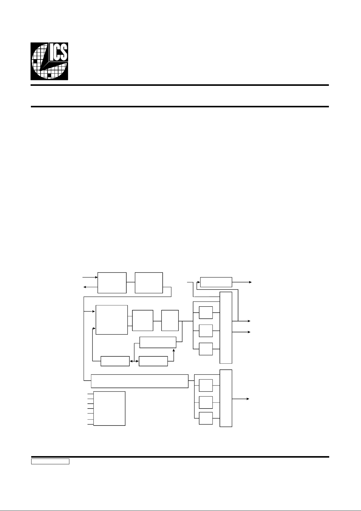
Block Diagram
XTAL1
XTAL2
Crystal
Oscillator
Reference
Divider
Charge
Pump
Phase-
Frequency
Comparator
EXTFREQ
VCO
Prescaler
/M
Strobe
FS0
FS1
FS2
FS3
MS0
MS1
/A
MCLK PLL (as above)
VCLK Set &
Program
Mode
Interface
MCLK Set
/2
/4
/8
/2
/4
MCLK
CLK-
CLK+
LOAD
/1, 4, 5 or 8
/8
Description
The ICS2572 is a dual-PLL (phase-locked loop) clock generator w ith differ ential vi deo outp uts spec ificall y design ed for
high-resolution, high-refresh rate, video applications. The
video PLL generates any of 16 pre-programmed frequencies
through selection of the address lines FS0-FS3. Similarly, the
auxiliary PLL can generate any one of four pre-programmed
frequencies via the MS 0 & MS1 line s.
A unique feature of the ICS2572 is the ability to redefine
frequency selections after power-up. This permits complete
set-up of the fre qu ency table upon system i nit ia l iz a ti on.
Features
•• Advanced ICS mono lithi c phase-l oc ked lo op
technology
•• Supports high-r esolution gr aphics - di fferential CLK out-
put to 185 MH z
•• Div ide d d o tc lock outp ut (L O A D ) a va il a ble
•• Simpl ified device pro gra m mi ng
•• Sixtee n se lect able VC LK fre q uenc ie s (all use r
re-programm able)
•• Four selectable MCLK frequencies (all user
re-programmable)
•• Windows NT compatible
Applications
•• High end PC/low end work sta ti on graphics designs
requiring diffe re ntial outp ut
•• X Termi na l gra ph ic s
E-95

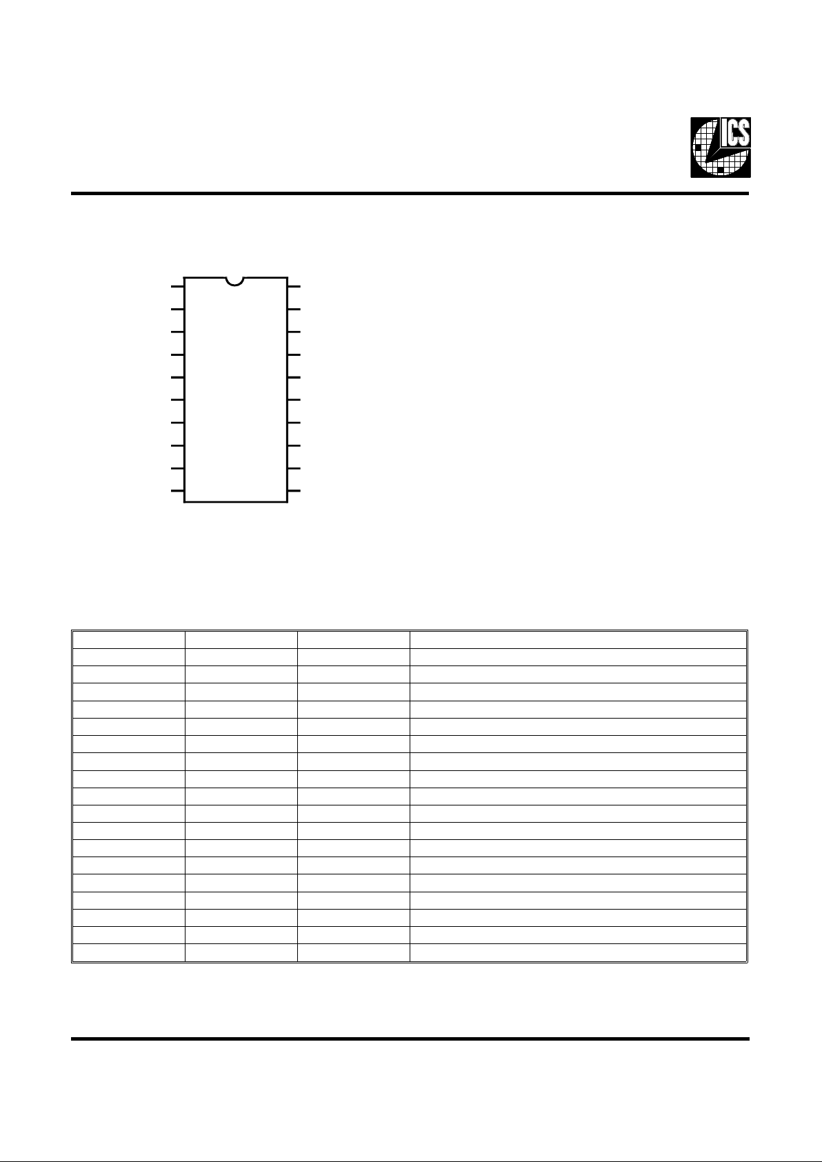
Pin Configuration
XTAL1 1 20 VDD
XTAL2 2 19 CLK+
XTFREQ 3 18 CLK-
FS0 4 17 VSS
FS1 5 16 LOAD
STROBE 6 15 VAA
FS2 7 14 VSS
FS3 8 13 VDD
MS0 9 12 MCLK
VSS 10 11 MS1
ICS2572
Pin Descriptions
PIN NUMBER PIN NAME TYPE DESCRIPTI ON
1 XTAL1 A Quartz crystal connection 1 /Referenc e Frequenc y Input.
2 XTAL2 A Quartz crystal conn ec tion 2.
3 EXTFRE Q I Externa l Fre qu en cy Input
4 FS0 I VCLK PLL Fre que nc y Sele ct LSB.
5 FS1 I VCLK PLL Fre que nc y Sele ct Bit.
7 FS2 I VCLK PLL Fre que nc y Sele ct Bit.
8 FS3 I VCLK PLL Fre que nc y Sele ct MSB.
6 STROBE I Control for Latch of VCLK Se lec t Bits (FS0-FS3).
9 MS0 I MCLK PLL Fre que nc y Sele ct LSB.
11 MS1 I MCLK PLL Fre que nc y Sele ct MSB.
19 CLK+ O Pixel Clock Output (not inverted)
18 CLK- O Pixel Clock Output (inverted)
16 LOAD O Divided Dotcloc k (/4 , 5, or 8)
12 MCLK O MCLK Frequency Output
17 RESERVE D - Must Be Connec t ed to VSS.
10, 14 VSS P Device Ground. All pins mu st be connected.
13, 20 VDD P Output Stage Vdd. All p ins must be conn ec ted .
15 VAA P Synthesizer Vdd.
20-Pin DIP or SOIC
J-4, J-7
ICS2572
E-96

Digital Inputs
The FS0-FS3 pins and the STROBE pin are used to select the
desired operating frequency of the VCLK output from the 16
pre-progr ammed/user -progr ammed select ions in the ICS2572.
These pins are also used to load new frequency data into the
registers.
A vai labl e conf igura tions for the ST ROBE input inclu de: posi tive-e dge triggered, negative-e dge triggered, high-level tra n sparent, and low-level tra nsparent (see Ordering Information).
VCLK Output Frequency Selection
To change the VCLK output frequency, simply write the appropriate data to the ICS2572 FS inputs. Do not perform any
further writes to the device for 50 milliseconds (assumes a
14.318 MHz reference). The synthesizer will output the new
frequency programmed into that location after a brief delay
(see timeout spec ific a tions).
MCLK Output Frequency Selection
The MS0-MS1 pins are used to directly select the desired
operating frequency of the MCLK output from the four preprogrammed/user-programmed selections in the ICS2572.
These inp uts are not latc hed, nor are th ey involve d with me mory programming operations.
Programming Mode Selection
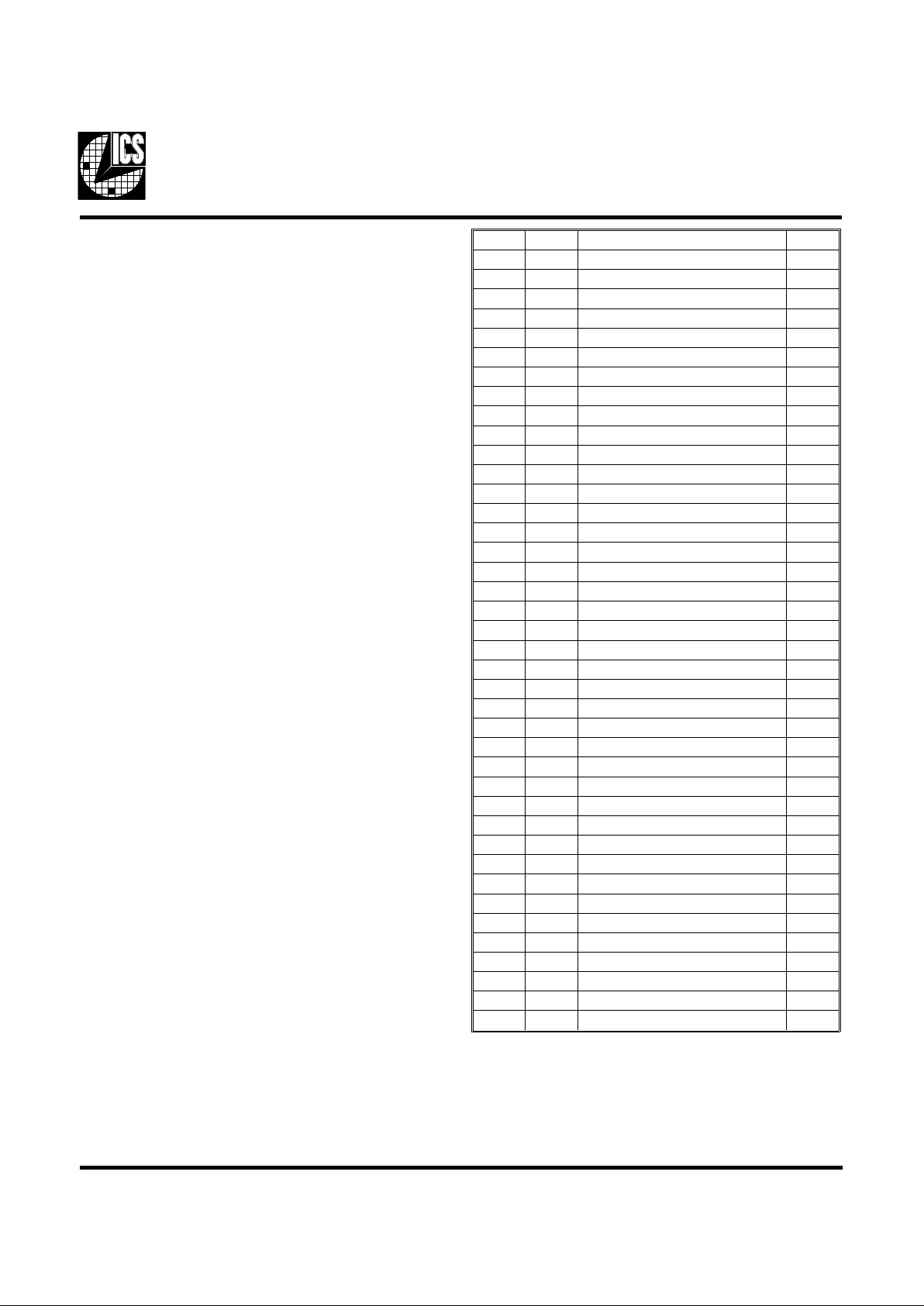
A programmi ng s eq uence is def ined as a p erio d of at l ea s t 5 0
milliseconds of no data writes to the ICS2572 (to clear the shift
register) followed by a series of data writes (as shown here):
FS0 FS1 FS2 FS3
XXSTART bit (must be “0”) 0
XX ” 1
XXR/W* cont rol 0
XX ” 1
XXL0 (location LSB ) 0
XX ” 1
XXL1 0
XX ” 1
XXL2 0
XX ” 1
XXL3 0
XX ” 1
XXL4 (location MSB) 0
XX ” 1
XXN0 (feedba ck LSB) 0
XX ” 1
XXN1 0
XX ” 1
XXN2 0
XX ” 1
XXN3 0
XX ” 1
XXN4 0
XX ” 1
XXN5 0
XX ” 1
XXN6 0
XX ” 1
XXN7 (feedback MSB) 0
XX ” 1
XXEXTFREQ bit (selected if “1”) 0
XX ” 1
XXD0 (post-divide r LSB) 0
XX ” 1
XXD1 (post-divider MSB) 0
XX ” 1
XXSTOP1 bit (mus t be “1” 0
XX ” 1
XXSTOP2 bit (must be “1”) 0
XX ” 1
ICS2572
E-97
 Loading...