

Integrated
Circuit
ICS1523
Systems, Inc.
High-Performance Programmable Line-Locked Clock Generator
General Description Features
The ICS1523 is a low-cost but very high-performance
frequency generator for line-locked and genlocked highresolution video applications. Using ICSs advanced
low-voltage CMOS mixed-mode technology, the ICS1523
is an effective clock solution for video projectors and displays at resolutions from VGA to beyond UXGA.
The ICS1523 offers pixel clock outputs in both differential
(to 250 MHz) and single-ended (to 150 MHz) formats.
Dynamic Phase Adjust circuitry allows user control of
the pixel clock phase relative to the recovered sync signal.
A second differential output at half the pixel clock rate
enables deMUXing of multiplexed analog-to-digital converters. The FUNC pin provides either the regenerated
input from the phase-locked loop (PLL) divider chain output or a re-synchronized and sharpened input HSYNC.
The advanced PLL uses either its internal programmable
feedback divider or an external divider. The device is programmed by a standard I
available in a 24-pin wide small-outline integrated circuit
(SOIC) package.
2
C-bus serial interface and is
Pixel clock frequencies up to 250 MHz
Very low jitter
Dynamic Phase Adjust (DPA) for clock outputs
Balanced PECL differential outputs
Single-ended SSTL_3 clock outputs
Double-buffered PLL/DPA control registers
Independent software reset for PLL/DPA
External or internal loop filter selection
Uses 3.3Vdc. Inputs are 5V-tolerant.
I2C-bus serial interface can run at either low speed
(100 kHz) or high speed (400 kHz).
Lock detection
24-pin 300-mil SOIC package
Applications
LCD monitors and video projectors
Genlocking multiple video subsystems
Frequency synthesis
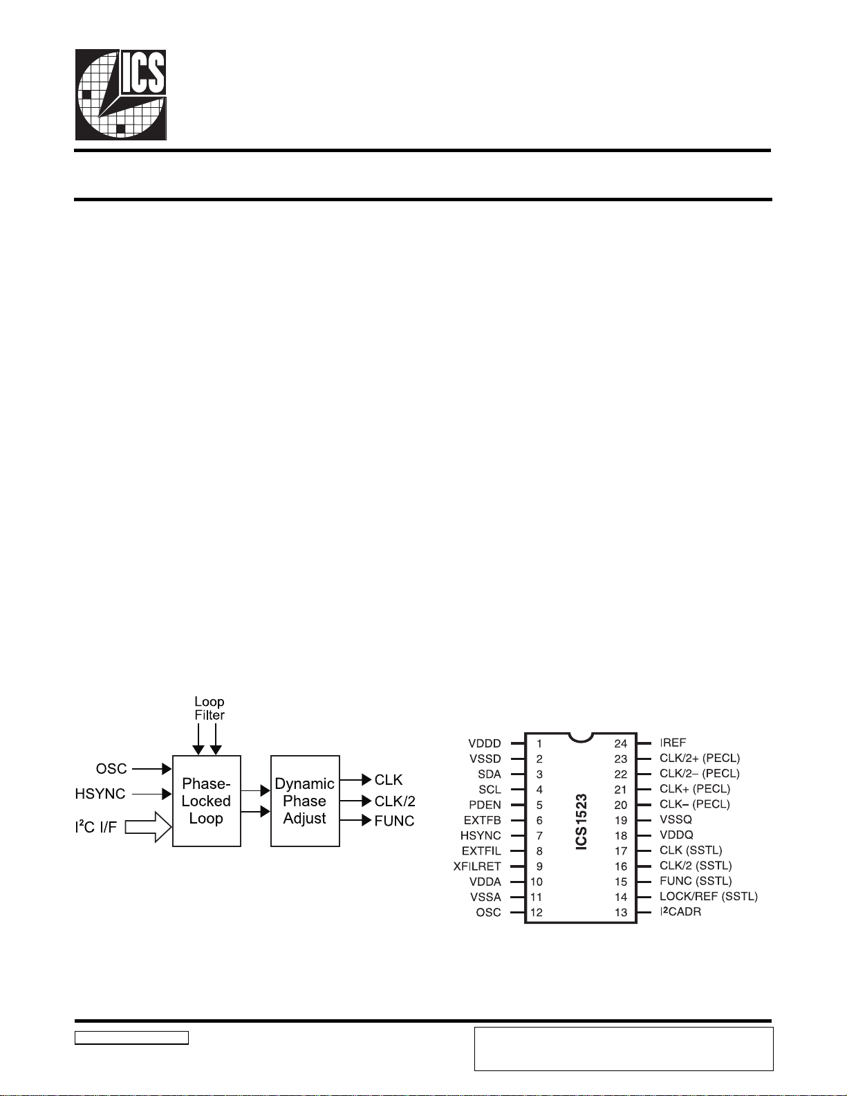
Block Diagram
I2C-bus is a trademark of Philips Corporation.
Dynamic Phase Adjust is a trademark of Integrated Circuit Systems, Inc.
ICS1523 Rev S 5/21/99
Pin Configuration
24-Pin SOIC
ICS reserves the right to make changes in the device data identified in
this publication without further notice. ICS advises its customers to
obtain the latest version of all device data to verify that any
information being relied upon by the customer is current and accurate.

ICS1523
Document Revision History
Rev P (First Release)
Pin Descriptions changed to add type column. (pg 3)
Added SDA and AC Input Characteristics. (pg 18)
Changed VCO Output, Intrinsic Jitter graph to show slow and fast cases (pg 19)
Timing diagram changes to reference t0 to REF and notes on test conditions added (pg 22)
Lock Renamed Lock/Ref (Throughout).
General cleanup for readability.
Rev Q
Added typical external loop filter values. (pg 17)
Added section on power supply considerations and SSTL_3 outputs. (pg 18)
Correct labels and scale on VCO Output, Intrinsic Jitter graph. (pg 20)
Correct depiction of timing diagram and added typical transition timing. (pg 23)
Added Document Revision History. (pg 25)
Rev R
Change to descriptions for pins 20 to 23. (pg 3)
Change to description for Reg 0h bits 0 and 1, added table. (pg 6)
Within table for Reg 0h bits 6 and 7, changed Osc_En to IN_SEL . (pg 6)
Moved Reg 0 bits 4 through 7 from pg 6 to new pg 7.
Change to Software Programming Flow diagram. (pg 13).
Added under Absolute Maximum Ratings ESD ratings and warning. (pg 19)
Under Recommend Operating Conditions, PECL Outputs, Output Low Voltage, added a note and added a new page. (pg 19)
Under Recommend Operating Conditions, SSTL-3 Outputs, Output Low Voltage, changed direction of symbols. (pg 19)
Change to VCO Output Frequency and Intrinsic Jitter graph to reflect correct VCO frequency (pg 20)
Rev S
Moved Revision History from last page of data sheet to second page. (pg 2)
In Layout Guideline 2, changed shunt capacitor value from 150 pF to 33 pF. (pg 19)
Changed various cross-references within Layout Guidelines. (pg 19)
2

Overview
ICS1523
The ICS1523 addresses stringent graphics system line-locked
and genlocked applications and provides the clock signals
required by high-performance video analog-to-digital converters. Included are a phase-locked loop (PLL) with a 500-MHz
voltage controlled oscillator (VCO), a Dynamic Phase Adjust to
provide a user-programmed pixel clock delay, the means for
deMUXing multiplexed ADCs, and both balanced-programmable (PECL) and single-ended (SSTL_3) high-speed clock
outputs.
Phase-Locked Loop
The phase-locked loop is optimized for line-locked applications, for which the inputs are horizontal sync signals. A
high-performance Schmitt trigger preconditions the HSYNC
input, whose pulses can be degraded if they are from a remote
source. This preconditioned HSYNC signal is provided as a
clean reference signal with a short transition time. (In contrast,
the signal that a typical PC graphics card provides has a transition time of tens of nanoseconds.)
A second high-frequency input such as a crystal oscillator and
a 7-bit programmable divider can be selected. This selection allows the loop to operate from a local source and is also useful
for evaluating intrinsic jitter.
A 12-bit programmable feedback divider completes the loop.
Designers can substitute an external divider.
Either the conditioned HSYNC input or the loop output (recovered HSYNC) is available at the FUNC pin, aligned to the edge
of the pixel clock.
Dynamic Phase Adjust
The Dynamic Phase Adjust allows addition of a programmable delay to the pixel clock output, relative to the recovered
HSYNC signal. The ability to add delays is particularly useful
when multiple video sources must be synchronized. A delay of
up to one pixel clock period is selectable in the following
increments:
1/64 period for pixel clock rates to 40 MHz
1/32 period for pixel clock rates to 80 MHz
1/16 period for pixel clock rates to 160 MHz
Output Drivers and Logic Inputs
The ICS1523 utilizes low-voltage TTL (LVTTL) inputs as well
as SSTL_3 (EIA/JESD8-8) and low-voltage PECL (pseudoECL) outputs, operating at 3.3-V supply voltage. The LVTTL
inputs are 5 V-tolerant. The SSTL_3 and differential PECL output drivers drive resistive terminations or transmission lines.
At lower clock frequencies, the SSTL_3 outputs can be operated unterminated.
I2C-bus Serial Interface
The ICS1523 utilizes the industry-standard I2C-bus serial interface. The interface uses 12 registers: one write-only, eight
read/write, and three read-only. Two ICS1523 devices can be
addressed, according to the state of the I2CADR pin. When
the pin is low, the read address is 4Dh, and the write address is
4Ch. When the pin is high, the read address is 4Fh, and the
write address is 4Eh. The I2C-bus serial interface can run at either low speed (100 kHz) or high speed (400 kHz) and provides
5V-tolerant input.
Automatic Power-On Reset Detection
The ICS1523 has automatic power-on reset detection circuitry
and it resets itself if the supply voltage drops below threshold
values. No external connection to a reset signal is required.
3
ICS1523
Pin Descriptions
.ONNIPEMANNIPEPYTNOITPIRCSEDSTNEMMOC
1DDDVRWPylppuslatigiDsnoitceslatigidotV3.3
2DSSVRWPdnuorglatigiD
3ADSTUO/NIatadlaireSI
4LCSNIkcolclaireSI
5NEDPNIelbaneDFPpmupegrahcsdnepsuS
6BFTXENInikcabdeeflanretxEottupniredividlanretxEDFP
7CNYSHNIcnyslatnoziroHLLPottupnikcolC
8LIFTXENIretliflanretxEretlifpoolLLPlanretxE
9TERLIFXNInruterretliflanretxEnruterretlifpoolLLPlanretxE
01ADDVRWPylppusgolanAyrtiucricgolanarofV3.3
11ASSVRWPdnuorggolanAyrtiucricgolanarofdnuorG
21CSONIrotallicsOrotallicsolatsyrcmorftupnIegakcap
31I2RDACNII2sserddaC
41
51)LTSS(CNUFTUOtuptuonoitcnuFtuptuoCNYSHelbatceles3_LTSS
61)LTSS(2/KLCTUOtuo2/kcolclexiPtupniXUMedCDAotrevird3_LTSS
71)LTSS(KLCTUOtuokcolclexiPCDAotrevird3_LTSS
81QDDVRWPylppusrevirdtuptuOsrevirdtuptuootV3.3
91QSSVRWPdnuorgrevirdtuptuOsrevirdtuptuorofdnuorG
02)LCEP(–KLCTUOtuokcolclexiP.niardnepO.CDAotrevirdLCEPdetrevnI
12)LCEP(+KLCTUOtuokcolclexiP.niardnepO.CDAotrevirdLCEP
22)LCEP(–2/KLCTUOtuo2/kcolclexiP
32)LCEP(+2/KLCTUOtuo2/kcolclexiP .niardnepO.tupniXUMedCDAotrevirdLCEP
42FERINItnerrucecnerefeRstuptuoLCEProftnerrucecnerefeR
)LTSS(
2
1
sub-C
2
1
sub-C
1
1
1
2,1
2
IpihC
tcelessserddaC
etirwhC4,daerhD4=woL
etirwhE4,daerhF4=hgiH
FER/KCOL
TUOecnerefer/rotacidnikcoLtupniFERrokcolAPDroLLPsyalpsiD
.tupniXUMedCDAotrevirdLCEPdetrevnI
.niardnepO
Notes:
1. These LVTTL inputs are 5 V-tolerant.
2. Connect to ground if unused.
4
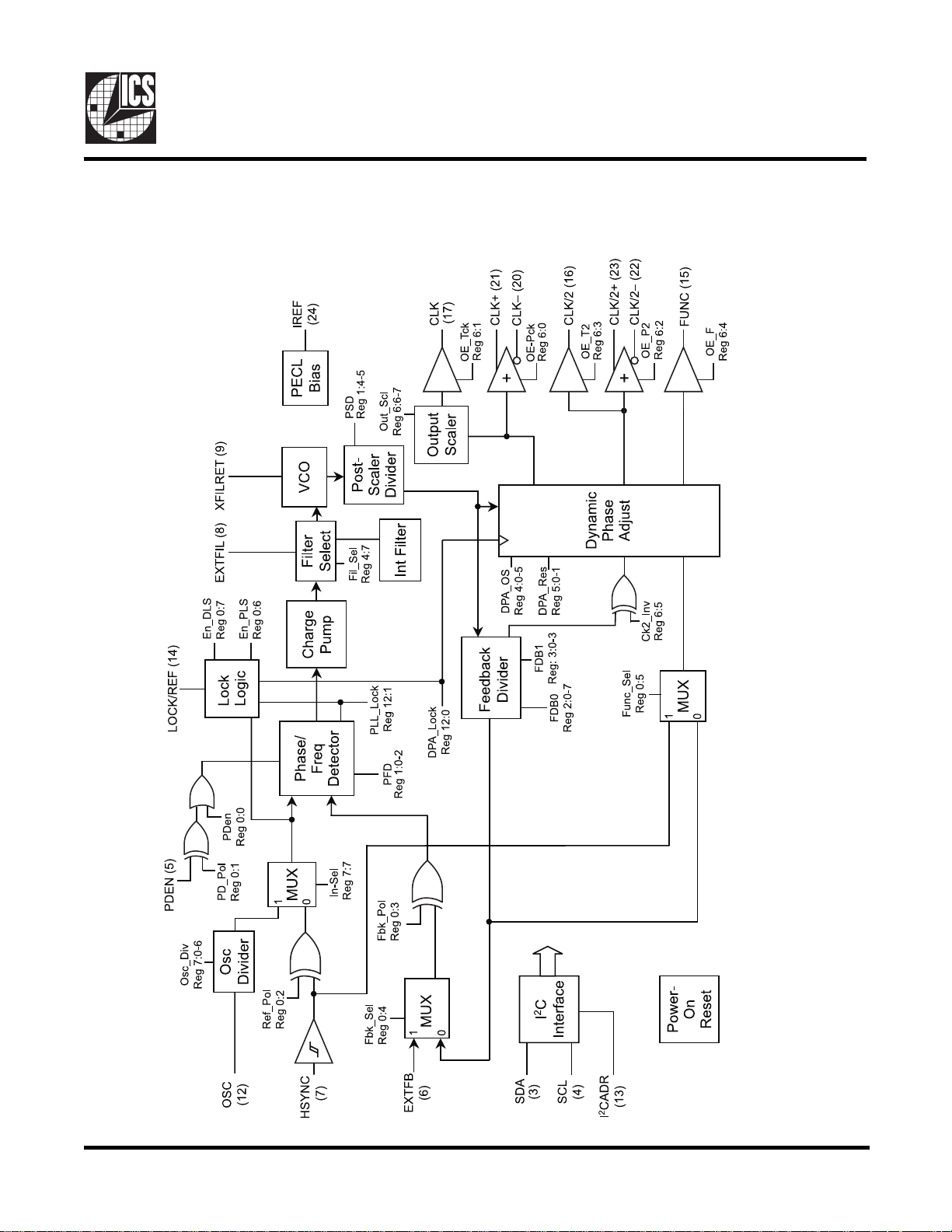
Block Diagram
ICS1523
5
ICS1523
I2C Register Map Summary
Register
Index
0h
1h
2h
3h
4h
5h
Name Access Bit Name Bit #
Input Control R / W PDen 0 1 Phase Detector Enable (0=External Enable, 1=Always Enabled)
PD_Pol 1 0 Phase Detector Enable Polarity (0=Not Inverted, 1=Inverted)
Ref_Pol 2 0 External Reference Polarity (0=Positive Edge, 1=Negative Edge)
Fbk_Pol 3 0 External Feedback Polarity (0=Positive Edge, 1=Negative Edge)
Fbk_Sel 4 0 External Feedback Select (0=Internal Feedback, 1=External)
Func_Sel 5 0 Function Out Select (0=Recovered HSYNC, 1=Input HSYNC)
EnPLS 6 1 Enable PLL Lock/Ref Status Output (0=Disable 1=Enable)
EnDLS 7 0 Enable DPA Lock/Ref Status Output (0=Disable 1=Enable)
Loop Control R / W * PFD0-2 0-2 0 Phase Detector Gain
Reserved 3 0 Reserved
PSD0-1 4-5 0 Post-Scaler Divider (0 = ÷2, 1 = ÷4, 2 = ÷8, 3 = ÷16)
Reserved 6-7 0 Reserved
FdBk Div 0 R / W * FBD0-7 0-7 FF PLL FeedBack Divider LSBs (bits 0-7) *
FdBk Div 1 R / W * FBD8-11 0-3 F PLL Feedback Divider MSBs (bits 8-11) *
Reserved 4-7 0 Reserved
DPA Offset R / W DPA_OS0-5 0-5 0 Dynamic Phase Aligner Offset
Reserved 6 0 Reserved
Fil_Sel 7 0 Loop Filter Select (0=External, 1=Internal)
DPA Control R / W ** DPA_Res0-1 0-1 3 DPA Resolution (0=16 delay elements, 1=32, 2=Reserved, 3=64)
Metal_Rev 2-7 0 Metal Mask Revision Nu mb er
Reset
Value
Description
6h
7h
8h
10h
11h
12h
Output Enables R / W OE_Pck 0 0 Output Enable for PECL PCLK Outputs ( 0=High Z, 1=Enabled)
OE_Tck 1 0 Output Enable for STTL_3 CLK Output ( 0=High Z, 1=Enabled)
OE_P2 2 0 Output Enable for PECL CLK/2 Outputs ( 0=High Z, 1=Enabled)
OE_T2 3 0 Output Enable for STTL_3 CLK/2 Output ( 0=High Z, 1=Enabled)
OE_F 4 0 Output Enable for STTL_3 FUNC Output ( 0=High Z, 1=Enabled)
Ck2_Inv 5 0 CLK/2 Invert (0=Not Inverted, 1= Inverted)
Out_Scl 6-7 0 SSTL Clock Scaler (0 = ÷1, 1 = ÷2, 2 = ÷4, 3 = ÷8)
Osc_Div R / W Osc_Div 0-6 0-6 0 Osc Divider modulus
In-Sel 7 1 Input Select (0=HSYNC Input, 1=Osc Divider)
Reset Write DPA 0-3 x Writing xAh resets DPA and loads working register 5
PLL 4-7 x Writing 5xh resets PLL and loads working registers 1-3
Chip Ver Read Chip Ver 0-7 17 Chip Version 23 Dec (17 Hex) as in 1523
Chip Rev Read Chip Rev 0-7 01 Initial value 01h. Value Increments with each all-layer change.
Rd_Reg Read DPA_Lock 0 N/A DPA Lock Status (0=Unlocked, 1=Locked)
PLL_Lock 1 N/A PLL Lock Status (0=Unlocked, 1=Locked)
Reserved 2-7 0 Reserved
* Identifies double-buffered registers. Working registers are loaded during software PLL reset.
** Identifies double-buffered register. Working registers are loaded during software DPA reset.
6
Detailed Register Description
Name: Input Control
Register: 0 h
Index: Read /Write
Bit Name Bit # Reset Value Description
PDen 0 1 Phase/Frequency Detector Enable
PD_Pol 1 0 Phase/Frequency Detector Enable Polarity
Ref_Pol 2 0 Phase/Frequency Detector External Reference Polarity
Fbk_Pol 3 0 External Reference Feedback Polarity
Fbk_Sel 4 0 External Feedback Select
Func_Sel 5 0 Function Output Select
EnPLS 6 1 Enable PLL Lock Status Output on LOCK/REF pin
EnDLS 7 0 Enable DPA Lock Status Output on LOCK/REF pin
Bit Name Description
ICS1523
0 PDen Phase/Frequency
Detector Enable
1 PD_Pol Phase/Frequency Detector
Enable Polarity
2 Ref_Pol Phase/Frequency Detector External Reference Polarity
Edge of input signal on which Phase Detector triggers.
0 = Rising Edge (default)
1 = Falling Edge
3 Fbk_Pol External Reference Feedback Polarity Edge of EXTFB (pin 6) signal on which
Phase/Frequency Detector triggers when external feedback is used (Reg0 [4]=1).
0 = Positive Edge (default)
1 = Negative Edge
Table continues on next ppage
neDPloP_DP
00 1=NEDP
X1 )tluafeD(syawlA
10 0=NEDP
rotceteDycneuqerF/esahP
:nehWdelbanEsI
7
ICS1523
Name: Input Control
Register: 0 h
Bit Name Description
4 Fbk_Sel External Feedback Select
0 = Internal Feedback (default)
1 = External Feedback
5 Func_Sel Function Output Select Selects re-clocked output to FUNC (pin 15).
0 = Recovered HSYNC (default). Re-generated HSYNC output.
1 = External HSYNC. Schmitt-trigger conditioned input from HSYNC (pin 7).
6 EnPLS Enable PLL Lock Status Output
on LOCK/REF pin
7 EnDLS Enable DPA Lock Status Output
on LOCK/REF pin
Bits 6, 7 enable multiple functions
at LOCK/REF, (pin 14)
SLPnESLDnELES_NI)41(FER/KCOL
00 A/N0
01 A/Nesiwrehto0,dekcolAPDfi1
10 A/Nesiwrehto0,dekcolLLPfi1
110
111 F
¸
cso
reggirtttimhcStsoP
loP_feRROX)7(CNYSH
viD_csO
8
Name: Loop Control Register
Register: 1h
Index: Read /Write*
Bit Name Bit # Reset Value Description
PFD0-2 0 - 2 0 Phase Frequency Detector Gain
Reserved 3 0 Reserved
PSD 0 -1 4 - 5 0 Post-Scaler Divider
Reserved 6-7 0 Reserved
Bit Name Description
0-2 PFD0-2 Phase/Frequency Detector Gain
2tiB1tiB0tiB2/Aµ(niaGDFP π )dar
000 1
001 2
010 4
011 8
100 61
101 23
110 46
111 821
ICS1523
3 Reserved
4-5 PSD 0-1 Post-Scaler Divider Divides the output of the VCO to the DPA and Feedback Divider.
5tiB4tiBrediviDDSP
00 )tluafed(2
01 4
10 8
11 61
6-7 Reserved
Double-buffered register. Actual working registers are loaded during software PLL reset.
*
See register 8h for details.
9

ICS1523
Name: Feedback Divider 0 Register / Feedback Divider 1 Register
Register: 2h, 3h
Index: Read /Write*
Bit Name Index Bit # Reset Value Description
FBD 0-7 2 0-7 FF PLL Feedback Divider LSBs (0-7).* When Bit 0 = 0, then the total
number of pixels is even. When Bit 0 = 1, then the total number of
pixels is odd.
FBD8-11 3 0-3 F PLL Feedback Divider MSBs (8 -11)*
Reserved 3 4-7 Reserved
The value that is programmed into these two registers, plus a value of 8, defines the total number of clock periods that the ICS
1523 generates between HSYNCs. Program these registers with the total number of horizontal pixels per line minus 8.
3geR2geR
321076543210
Feedback Divider Modulus
=
12 £ Feedback Divider Modulus £ 4103
+8
Double-buffered registers. Actual working registers are loaded during software PLL reset.
*
See Register 8h for details.
Name: DPA Offset Register
Register: 4 h
Index: Read /Write
Bit Name Bit # Reset Value Description
DPA_OS0-5 0 -5 0 Dynamic Phase Adjust Offset
Reserved 6 0 Reserved
Fil_Sel 7 0 Loop Filter Select
Bit Name Description
0-5 DPA_OS0-5 Dynamic Phase Adjust Offset.
Selects clock edge offset in discrete steps from zero to one clock period minus one step.
Resolution (number of delay elements per clock cycle) is selected by DPA_Res0-1 (Reg 5:0-1).
Note: Offsets equal to or greater than one clock period are neither recommended nor supported.
Example: For DPA_Res0-1=01H, the clock can be delayed from 0 to 31 steps.
7 Fil_Sel Selects external loop filter (0) or internal loop filter (1).
The use of an external loop filter is strongly recommended for all designs. Suggested component
values are available from the ICS1523 Demo Board Guide (1523DB.pdf) or the ICS1523 Register
Tool (inst1523.exe) available on our web site at: (http://www.icst.com/products/pinfo/1523.htm).
10

Name: DPA Control Register
g
Register: 5h
Index: Read /Write*
Bit Name Bit # Reset Value Description
DPA_Res0-1 0-1 3 Dynamic Phase Adjust Resolution Select.
Metal_Rev 2-7 0 Metal Mask Revision Number.
Bit Name Description
0-1 DPA_Res0-1 Dynamic Phase Adjust (DPA) Resolution Select.
It is not recommended to use the DPA above 160 MHz.
ICS1523
Bit 1 Bit 0 Delay Elements
0 0 16 48 160
0 1 32 24 80
10 Reserved
1 1 64 12 40
2-7 Metal_Rev Metal Mask Revision Number.
After power-up, register bits 7:2 must be written with 111111. After this write,
a read indicates the metal mask revision, as below.
noisiveR7tiB6tiB5tiB4tiB3tiB2tiB
A 111111
B 011111
1C 101111
2C 001111
D110111
E 111011
F 111101
G 111110
CLK Ra n
e, MHz
Double-buffered register. Actual working registers are loaded during software DPA reset.
*
See register 8h for details.
11

ICS1523
Name: Output Enable Register
Register: 6 h
Index: Read /Write
Bit Name Bit # Reset Value Description
OE_Pck 0 0 Output Enable for CLK Outputs (PECL)
OE_Tck 1 0 Output Enable for CLK Output (SSTL_3)
OE_P2 2 0 Output Enable for CLK/2 Outputs (PECL)
OE_T2 3 0 Output Enable for CLK2 Output (SSTL_3)
OE_F 4 0 Output Enable for FUNC Output (SSTL_3)
Ck2_Inv 5 0 CLK/2 Invert
Out_Scl 6-7 0 CLK Scaler
Bit Name Description
0 OE_Pck Output Enable for CLK Outputs (PECL)
0 = High Z
1 = Enabled
1 OE_Tck Output Enable for CLK Output (SSTL_3)
0 = High Z
1 = Enabled
2 OE_P2 Output Enable for CLK/2 Outputs (PECL)
0 = High Z
1 = Enabled
3 OE_T2 Output Enable for CLK/2 Output (SSTL_3)
0 = High Z
1 = Enabled
4 OE_F Output Enable for FUNC Output (SSTL_3)
0 = High Z
1 = Enabled
5 Ck2_Inv CLK/2 Invert
0 = Not Inverted
1 = Inverted
6-7 Out_Scl Clock (CLK) Scaler
7tiB6tiBrediviDKLC
00 1
01 2
10 4
11 8
12

Name: Oscillator Divider Register
Register: 7h
Index: Read /Write
Bit Name Bit # Reset Value Description
Osc_Div 0-6 0-6 0 Osc Divider Modulus
In_Sel 7 1 Input Select
Bit Name Description
0- 6 Osc_Div 0-6 Oscillator Divider Modulus.
Divides the input from OSC (pin 12) by the set modulus.
The modulus equals the programmed value, plus 2.
Therefore, the modulus range is from 3 to 129.
7 In_Sel Input Select Selects the input to the Phase/Frequency Detector
0 = HSYNC
1 = Osc Divider
ICS1523
Name: RESET Register
Register: 8 h
Index: Write
Bit Name Bit # Reset Value Description
DPA Reset 0-3 x Writing xAh to this register resets DPA working register 5
PLL Reset 4-7 x Writing 5xh to this register resets PLL working registers 1-3
Bit Name Description
0 -3 DPA Writing xAh to this register resets DPA working register 5
4-7 PLL Writing 5xh to this register resets PLL working registers 1-3
eulaVsteseR
AxAPD
x5LLP
A5LLPdnaAPD
13

ICS1523
Name: Chip Version Register
Register: 10 h
Index: Read
Bit Name Bit # Reset Value Description
Chip Ver 0-7 17 Chip Version 23 (17h)
Name: Chip Revision Register
Register: 11h
Index: Read
Bit Name Bit # Reset Value Description
Chip Rev 0 -7 01+ Initial value 01h.
+Value increments with each all-layer change.
Name: Status Register
Register: 12 h
Index: Read
Bit Name Bit # Reset Value Description
DPA_Lock 0 N/A DPA Lock Status
PLL_Lock 1 N/A PLL Lock Status
Reserved 2-7 0 Reserved
Bit Name Description
0 DPA_Lock DPA Lock Status. (Refer to Register 0h, bits 6 and 7.)
0 = Unlocked
1 = Locked
1 PLL_Lock PLL Lock Status. (Refer to Register 0h, bits 6 and 7.)
0 = Unlocked
1 = Locked
2-7 Reserved
14

ICS1523 Software Programming Flow
ICS1523
15

ICS1523
I2C Data Characteristics
Bit transfer on the I2C-bus
START and STOP conditions
Acknowledge on the I2C-bus
These waveforms are from "The I2C-bus and how to use it," published by Philips Semiconductor.
The document can be obtained from http://www-us2.semiconductors.philips.com/acrobat/various/i2c_bus_specification_1995.pdf
16

ICS1523
a
a
a
a
a
a
:
I2C Data Format
RANDOM REG ISTER WRIT E PRO CEDURE
S010011xWA A AP
7 bit address register address dat
Acknowledge Acknowledge STOP condition
START condition WRITE command Acknowledge
RANDOM REG ISTER READ PROCEDURE
S010011XWA AS010011XRA AP
7 bit address register address 7 bit address dat
Acknowledge Repeat START Acknowledge STOP condition
START condition WRITE command Acknowledge READ command NO Acknowledge
SEQUENTIAL REGISTER WRITE PROCEDURE
S010011XWA A A A AP
7 bit address register address dat
Acknowled ge Acknowledge Acknowledge Ackno w l edge Acknowledge
START condition WRITE command STOP condition
dat
SEQUENTIAL REGISTER READ PROCEDURE
S010011XWA AS010011XRA A AP
7 bit address register address 7 bit address dat
Acknowledge Repeat START Acknowledge NO Acknowledge
START condition WRITE command Acknowledge READ command Acknowledge STOP condition
Direction
From bus host to device From device to bus host
dat
Note:
1. All values are transmitted with the most-significant bit first and the least-significant bit last.
2. The value of the X bit equals the logic state of pin 13 (I2CADR).
3. R = READ = 1 and W = WRITE = 0
17

ICS1523
ICS1523 Video Mode Reference Table
The use of an external loop filter is strongly recommended in All Designs.
The ICS1523 Video Mode Reference Table (previously included in this data sheet) lists information on the various video modes
that can be used with the ICS1523. To reference this table, see the ICS1523 Demo Board Guide (1523DB.pdf) available on our
web site at: (http://www.icst.com) under the ICS1523 area.
18

General Layout Guidelines
ICS1523
Use a PC board with at least four layers: one power, one
ground, and two signal.
No special cutouts are required for power and ground
planes.
All supply voltages must be supplied from a common
source and must ramp up together.
Flux and other board surface debris can degrade the perfor-
mance of the external loop filter. Ensure that the 1523 area of
the board is free of contaminants.
Specific Layout Guidelines
1. Digital Supply (VDD) Bypass pin 1 (VDD) to pin 2
(VSS) with 4.7-µF and 0.1-µF capacitors, located as close
as possible to the pins. Traces must be maximally wide and
include multiple surface-etched vias to the appropriate
plane.
2. External Loop Filter The use of an external loop fil-
ter is strongly recommended in All Designs. Locate loop
filter components as close to pins 8 and 9 (EXTFIL and
EXTFILRET) as possible. Typical loop filter values are
6.8K W for the series resistor, 3300 pF RF-type capacitor for
the series capacitor, and 33 pF for the shunt capacitor. (For
details, see the Frequently Asked Questions part of the
ICS1523 Applications Guide, FAQ2 and FAQ3.).
5. PECL Outputs Implement these outputs as
microstrip transmission lines. The trace widths shown are
for 75W characteristic impedance, presuming .067 in.
between layers. Locate the optional series snubbing resistors as close as possible to the pins. If the termination
resistors are included on-board, locate them as close as
possible to the load and connect directly to the power and
ground planes.
[These termination resistors are omitted if the load device
implements them internally. For details, see the ICS application note on microstrip and striplines (1572AN1) and
within the ICS1523 Applications Guide, the application
note on Designing a Custom Interface for the ICS1523
(1523AN4.)]
6. Output Driver Supply Bypass pin 18 (VDDQ) to pin
19 (VSSQ) with 4.7-µF and 0.1-µF capacitors, located as
close as possible to the pins. Traces must be maximally
wide and include multiple surface-etched vias to the appropriate plane.
7. SSTL_3 Outputs SSTL_3 outputs can be used like
conventional CMOS rail-to-rail logic or as a terminated
transmission line system at higher-output frequencies.
With terminated outputs, the considerations of item 5,
PECL Outputs apply. See JEDEC documents JESD8-A
and JESD8-8.
3. Analog PLL Supply (VDDA) Decouple pin 10
(VDDA) with a series ferrite bead. Bypass the supply end
of the bead with 4.7-µF and 0.1-µF capacitors. Bypass pin
10 to pin 11 (VSSA) with a 0.1-µF capacitor. Locate these
components as close as possible to the pins. Traces must
be maximally wide and have multiple surface-etched vias to
the power or ground planes.
.
4. PECL Current Set Resistor Locate PECL current-
set resistor as close as possible to pin 24 (IREF). Bypass
pin 24 to ground with a 0.1 -µF capacitor.
1
2
1
ICS1523
3
Note: Drawing is not to scale. It is for illustrative purposes only.
19
4
5
6
7

ICS1523
Power Supply Considerations
The ICS1523 incorporates special internal power-on reset circuitry that requires no external reset signal connection. The supply
voltage (VDD) must remain within the recommended operating conditions during normal operation. To reset the ICS1523, the
supply voltage at the part must be reduced below the threshold voltage (Vth) of the power-on reset circuit. The supply voltage
must remain below that threshold voltage such that board power conditioning capacitors are drained and the proper reset state
is latched. The amount of time (td) to hold the voltage in a reset state varies with the design. However, a typical value of 10 ms
should be sufficient.
SSTL_3 Outputs
Unterminated Outputs
In the ICS1523, unterminated SSTL output pins display exponential transitions similar to those of rectangular pulses presented to
RC loads. The 10-90% rise time is typically 1.6 ns, and the corresponding fall time is typically 700 ps. In turn, this asymmetry
contributes to duty cycle asymmetry at higher output frequencies. In the absence of significant load capacitance (which can
further increase rise and fall time), this asymmetry is the dominant factor determining high-frequency performance of these singleended outputs. Typically, no termination is required either for the LOCK/REF, FUNC, and CLK/2 outputs or for CLK outputs up to
approximately 135 MHz.
T erminated Outputs
SSTL_3 outputs are intended to terminate in low impedances to reduce the effect of external circuit capacitance. Use of transmission line techniques enables use of longer traces between source and driver without increasing ringing due to reflections. Where
external capacitance is minimal and substantial voltage swing is required to meet LVTTL VIH and VOL requirements, the intrinsic
rise and fall times of ICS1523 SSTL outputs are only slightly improved by termination in a low impedance.
The ICS1523 SSTL output source impedance is typically less than 60W. Termination impedance of 100W reduces output swing by
less than 30% which is more than enough to drive a single load of LVTTL inputs.
20

Absolute Maximum Ratings
VDD, VDDA, VDDQ (measured to VSS) . . . . . . . . . . . . . . . . . 4.3 V
Digital Inputs . . . . . . . . . . . . . . . . . . . . . . . . . . . . . . . . . . . . . . . . . VSS 0.3 V to 5.5 V
Analog Outputs . . . . . . . . . . . . . . . . . . . . . . . . . . . . . . . . . . . . . . . VSSA 0.3 V to VDDA +0.3 V
Digital Outputs . . . . . . . . . . . . . . . . . . . . . . . . . . . . . . . . . . . . . . . VSSQ 0.3 V to VDDQ +0.3 V
Storage Temperature . . . . . . . . . . . . . . . . . . . . . . . . . . . . . . . . . . 65°C to +15 0°C
Junction Temperature . . . . . . . . . . . . . . . . . . . . . . . . . . . . . . . . . . 175°C
Soldering Temperature . . . . . . . . . . . . . . . . . . . . . . . . . . . . . . . . . 260°C
ESD Susceptibility* . . . . . . . . . . . . . . . . . . . . . . . . . . . . . . . . . . . > 2 KV
(*Electrostatic-sensitive devices. Do not open or handle except in a static-free workstation.)
ICS1523
21

ICS1523
Recommended Operating Conditions
VDD, VDDQ, VDDA (measured to VSS) . . 3.0 to 3.6 V
Operating Temperature (Ambient) . . . . . . . . . 0 to +70°C
tnerruCylppuSCD
RETEMARAPLOBMYSSNOITIDNOCNIMXAMSTINU
latigiD,tnerruCylppuSDDDIV6.3=DDDV—52Am
srevirDtuptuO,tnerruCylppuSQDDI.delbanesrevirdtuptuoon,V6.3=QDDV—6Am
golanA,tnerruCylppuSADDIV6.3=ADDV—5Am
RETEMARAPLOBMYSSNOITIDNOCNIMXAMSTINU
egatloVhgiHtupnIHIV25.5V
egatloVwoLtupnILIV3.0-SSV8.0V
siseretsyHtupnI 2.06.0V
tnerruChgiHtupnIHIIV
tnerruCwoLtupnILIIV
ecnaticapaCtupnIniC—01Fp
RETEMARAPLOBMYSSNOITIDNOCNIMXAMSTINU
egatloVwoLtuptuOLOV
RETEMARAPLOBMYSSNOITIDNOCNIMXAMSTINU
egatloVhgiHtuptuOHOV0=TUOI—DDVV
egatloVwoLtuptuO
).deniatniam
RETEMARAPLOBMYSSNOITIDNOCNIMXAMSTINU
ecnatsiseRtuptuOR
wolebllaftontsumLOV:etoN(
ehttahtosnevigleveleht
ebnacTUOIrofeulavtcerroc
LOVeulavdemmargorp=TUOI0.1—V
O
scitsiretcarahCtupnICA
RETEMARAPLOBMYSSNOITIDNOCNIMXAMSTINU
ycneuqerFtupnICNYSHf
ycneuqerFtupnICSOf
CNYSH
CSO
DDV=—01±Aµ
HI
0=—002±Aµ
LI
)lanoitceridiBsiADS:edoMtuptuOnI(ADS
KCOL,CNUF,2/KLC,KLC(stuptuO3-LTSS
V<1
V2<—08
O
0=7:7geR800.01zHM
1=7:7geR20.001zHM
2
,CSO,CNYSH,BFTXE,NEDP,LCS,ADS(stupnIlatigiDI
C)RDA
samumixamV0.6=HOV.Am3=TUOI
.rotsiserpu-lluplanretxeehtybdenimreted
4.0V
)–2/KLC,+2/KLC,–KLC,+KLC(stuptuOLCEP
)FER/
W
22

700
ICS1523
VCO Output Frequency and Intrinsic Jitter
700
VCO Frequency (MHz)
600
500
400
300
200
100
Frequency (Slow: 3.0V @ 70ºC)
Frequency (Nominal: 3.3V @ 30ºC)
Frequency (Fast: 3.6V @ 0ºC)
Jitter (3.0 V @ 70ºC)
Jitter (3.3 V @ 30ºC)
Jitter (3.6 V @ 0ºC)
Frequency
Jitter
0
8
6
8
0
2
.
0
0
6
4
.
.
0
0
1
.
1
4
2
.
.
1
VCO Voltage
1
8
.
.
1
2
2
.
2
2
6
4
.
.
2
2
3
.
2
.
3
600
500
400
300
200
100
Jitter (ps)
0
23

ICS1523
ns Delay
ns Delay
DPA Delay-16 Elemen t Reso l ution
20
18
16
14
12
10
50 MHz - SVGA @ 72 Hz
157.5 MHz - SXGA @ 85 Hz
8
6
4
2
0
04812
DPA Settin g
DPA Delay - 32 Element Resoluti o n
45
40
35
30
25
20
15
10
5
0
25.175 MHz - VGA @ 60 Hz
78.75 MHz - XGA @ 75 Hz
0 4 8 1216202428
DPA Setting
16
32
DPA Delay - 64 Elemen t Resol u tio n
90
80
70
60
50
40
ns Delay
30
20
10
0
12.27 MHz - NTSC
39.8 MHz - SVGA @ 60
0 4 8 12 16 20 24 28 32 36 40 44 48 52 56 60
Note:
Maximum number of data points used for this graph.
DPA Setting
24
64

25
AC Timing Characteristics Overview
* Timing when Register 2, Bit 0 = 0 (Total number of pixels is even.)
** Timing when Register 2, Bit 0 = 1 (Total number of pixels is odd.)
ICS1523

ICS1523
Output Timing Diagram
Typical Transition Times*
lobmySnoitpircseDgnimiTesiRllaFstinU
t
R
t
P
t
S
t
F
FER8.28.1sn
KLCLCEP0.12.1sn
KLC-LTSS6.17.0sn
TUO_CNUF2.10.1sn
Output Timing*
lobmySnoitpircseDgnimiTniMpyTxaMstinU
t
0
t
1
t
2t,3
t
4
t
5
t
6
t
7
t
8t,9
*Note: Measured at 3.6V 0°C, 135-MHz output frequency, PECL clock lines to 75W termination, SSTL_3 clock lines
unterminated, 20-pF load. Transition times vary based on termination.
yaledFERotCNYSH3.115.1121sn
yaledkcolcLCEPotFER0.1-8.02.2sn
elcycytudkcolcLCEP540555%
yaledkcolc3_LTSSotkcolcLCEP2.057.02.1sn
yaledTUO_CNUFotkcolcLCEP5.19.13.2sn
kcolc2/LCEPotkcolcLCEP0.13.15.1sn
yaled2/KLC–3_LTSSotkcolcLCEP1.14.18.1sn
elcycytudkcolcLTSS540555%
26

ICS1523
Ordering Information
ICS1523M
24-Pin SOIC (wide body)
ICS reserves the right to make changes in the device data identified in
27
this publication without further notice. ICS advises its customers to
obtain the latest version of all device data to verify that any
information being relied upon by the customer is current and accurate.
 Loading...