

ICS82C404RevA111095
Integrated
Circuit
Systems, Inc.
ICS82C404
Advanc e Informa tion
General Description
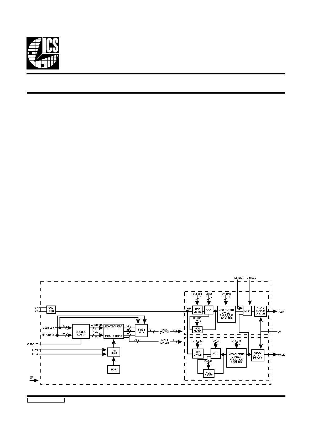
The ICS82C404 is a fully programmable graphics clock generator. It can generate user specified clock frequencies using
an exter nally generated input reference or by a single crystal.
The output frequency is programmed by entering a 24-bit
digital word through t he seri al port .
Two fully user-programmable phase-locked loops are offered
in a single packa ge. One PLL is designed to drive the mem ory
clock, while the second drives the video clock. The outputs
may be changed on-the-fly to any desired frequency between
390 kHz and 120 MHz. The ICS82C404 is ideally suited for
any desi gn whe re mult iple or varyin g freq uenc ies are require d.
This part is ideal for graphics applications. It generates low
jitter, high speed pixel clocks. It can be used to replace
multiple, expensive high speed crystal oscillators. The flexibility of the device allows it to generate non-standard graphics clock s .
The le ader in the ar ea of multip le clock ou tput clocks on a
single chip, ICS has been shipping graphics frequency generators since October, 1990, and is constantly improving the
phase-locked loop. The ICS82C404 incorporates a patented
fourth generation PLL that offers the best jitter performance
avai labl e.
Features
•• Pin-for-pin and function compatible with ICD’s version
of the 82C404
•• Dual programmable graphics clo ck generator
•• Memo ry and v ideo cloc ks are i ndivid uall y progra mm able
“on- the-f ly”
•• Ideal for designs where multiple or varying frequencies
are required
•• Increased frequency resolution from optional pre-divide-
by-2 on the M cou n te r
•• Output enable feature available for tristating outputs
•• Independent clock outputs range from 390 kHz to
120 MHz
•• Operation up to 140 MHz available
•• Power-down capabilit ies
•• Low-power , high speed 0.8 µ CMOS technology
•• Glitch-free transitions
•• Available in 16-pin PDIP or SOIC packa ge
Dual P rogram mable Graphi cs Freq uency Genera tor
Block Diagram
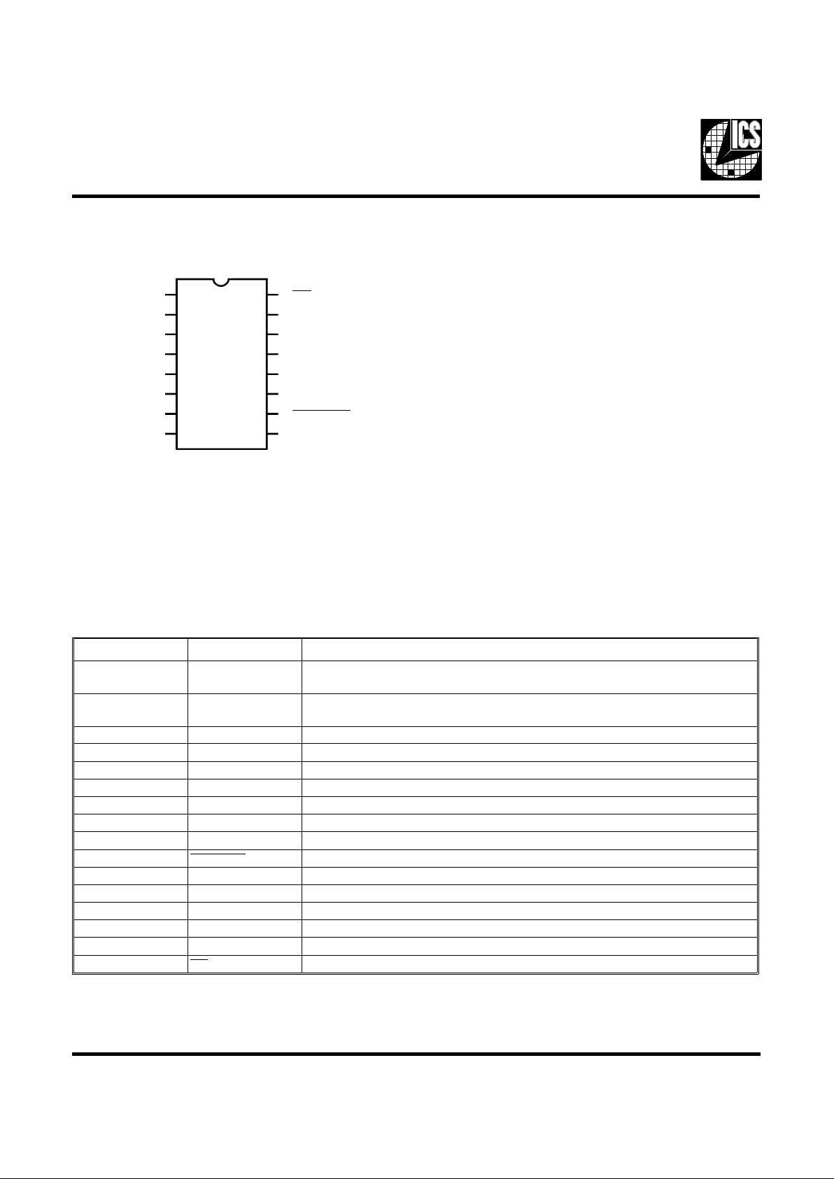
Pin Configuration
SEL0/CLK 1 16 PD
SEL1/DATA 2 15 EXTSEL
VDD 3 14 INIT1
OE 4 13 VDD
GND 5 12 INIT0
X1 6 11 EXTCLK
X2 7 10
FPMODE
MCLK 8 9 VCLK
ICS82C404
Pin Descriptions
PIN NUMBER PIN NAME DESCRIPTIO N
1 SEL 0-CL K Clock input in serial progra mm i ng m ode .
Clock select pin in operating mode.
2 SEL1-DATA Data input in serial programm ing m ode.
Clock select pin in operating mode.
3 AVDD Power.
4 OE Tri sta tes outp uts whe n lo w.
5 GND Ground.
6 X1 Crystal input.
7 X2 Crystal output.
8 MCLK Memory cloc k out put .
9 VCLK V i de o clock ou tpu t.
10
FPMODE Clock select input used to force REG2 pro gra m med fr eque nc y.
11 EXTCLK External clock input.
12 INIT0 Selects initial power-up conditions, LSB.
13 VDD Power.
14 INIT1 Selects initial power-up conditions, MSB.
15 EXTSEL Selects external clock input (EXTCLK) as VCLK output.
16
PD Power-down pin, active low.
16-Pin PDIP or SOIC
ICS82C404
2
Register Definitions
The register file c onsists of the following six registers:
Register Addr essing
Address Register Definition
000
001
010
011
100
110
REG0
REG1
REG2
MREG
PWRDWN
CNTL REG
Vi de o Cl oc k Re gist er 1
Vi de o Cl oc k Re gist er 2
Vi de o Cl oc k Re gist er 3
Memory Regist er
Divisor for Power - down m ode
Control Re gister
The ICS82C404 plac e s t he t hre e vi de o cloc k re gisters a n d t he
memory clock register in a known state upon power-up. The
regis ters are initia lized based on t he st ate of the IN IT1 a nd
INIT0 pins at applicatio n of power to the device. The INIT pins
must ramp up with VDD if a logical 1 on either pin is require d.
These input pins are inter nall y pulled d own and wi ll defa ult to
a logical 0 if left unconnected.
The registers a re initial ize d as follows:
Register Initialization
INIT1 INIT0 MREG REG0 REG1 REG2
0
0
1
1
0
1
0
1
32.500
40.000
50.350
56.644
25.175
25.175
40.000
40.000
28.322
28.322
28.322
50.350
28.322
28.322
28.322
50.350
Register Selection
When the ICS82C404 is operating, the video clock output is
control led with a comb inat ion of t he SEL 0, SEL 1,
PD, and OE
pins. The video clock is also multiplexed to an external clock
(EXTCLK) which can be selected with the EXTSEL pin. The
VCLK Select io n Table shows how VCLK is selecte d.
VCLK Selection
OE PD EXTSEL FPMODE SEL1 SEL0 VCLK
0
1
1
1
1
1
1
1
x
0
1
1
1
1
1
1
x
x
x
x
0
1
x
x
x
x
1
1
1
1
1
0
x
x
0
0
1
1
1
x
x
x
0
1
0
x
1
x
Tristate
Forced High
REG0
REG1
EXTCLK
REG2
REG2
REG2
As seen i n the table above, OE acts to tristate the outpu t. The
PD pin forces the VCLK signa l high while powering down the
part. The EXTCLK pin will only be multiplexed in when
EXTSEL and SE L 0 are logi c 0 and SE L1 is a logi c 1.
The memory clock outputs are controlled by
PD and OE as
follows:
MCLK Selection
OE PD MCLK
0
1
1
x
1
0
Tristate
MREG
PWRDWN
The Clock Selec t pins SEL0 a nd SEL 1 have two purp oses. In
serial prog ramming mod e, t hese pins act as the cl ock and data
pins. New da ta bits come in on SEL1 and t hese bits a re c locke d
in by a signal on SEL0. While these pins are acquiring new
information, the VCLK signal remains unchanged. When
SEL0 and SEL1 are acting as register selects, a time-out
interval is required t o determin e whet her t he user i s se le cting
a new register or wants to program the part. During this initial
time-out, the VCLK signal remains at its previous frequency.
At the end of this tim e -out int er va l, a ne w reg iste r i s sele c ted.
A second time-out interval is required to allow the VCO to
settle to its new value. During this period of time, typically 5 ms,
the input reference signal is multiplexed to the V CLK signal.
When MCLK or the active VCLK register is being reprogrammed, then the reference signal is multiplexed glitch-free
to the output during the first time-o ut interva l. A second timeout interva l is also re quire d to allow t he VCO to set tle. Du ring
this period, the re fere nce sign al is multipl exe d to t he a ppropri ate output signal.
ICS82C404
3
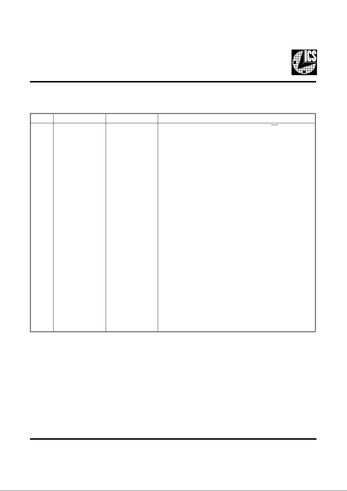
Control Register Definition
The contro l re gi ste r allo w s the user t o ad just var iou s internal option s. The re gist er is de fi ne d as fol lo w s:
Bit Bit Name Default Value Description
9
8
7
6
5
4
3
2
1
C5
C4
C3
C2
C1
C0
NS2
NS1
NS0
0
0
0
0
1
0
0
0
0
This bit determines which power -down mode the
PD pin will
implement . Power -d own mode 1, C5=0, forces the MCLK signa l to
be a function of the power- down re gi ste r. Power-d own m ode 2,
C5=1, turns of f the crysta l and disable s al l outpu ts.
This bit de te rm in es which cloc k is mu lt iplexed to VCL K duri ng
frequency changes. C4=0 multiplexes the reference frequency to the
VCLK output. C4=1 m ul ti ple xe s MCL K to th e VC LK o utput for
applic atio ns wh er e the gra phi cs c ont rol le r can not run as slow as
f
REF
.
This bit de te rm ines the len gth of the tim e- out int e rval. The tim e- out
interval is derive d fro m the MCLK VCO. If this VCO is
programme d to cert ain e xtr eme s, the time -ou t interva l maybe to o
short. C3=0, normal time-out. C3=1, doubled time -out interval.
Reserved, must be set to 0.
This bit adjust s the duty cycl e. C1=0 c a uses a 1ns dec re ase i n
output high time. C1=1 causes no adjustment. If the load
capacit ance is high, the adj ustm e nt ca n bri ng th e du ty cyc le close r
to 50%.
Reserved, must be set to 0.
Acts on register 2. NS2=0 presc a les the N cou nter by 2.
NS2=1 prescales the P counter val ue to 4.
Acts on register 1. NS1=0 presc a les the N cou nter by 2.
NS1=1 prescales the P counter val ue to 4.
Acts on register 0. NS0=0 presc a le s the P counter by 2.
NS0=1 prescales the P counter val ue to 4.
ICS82C404
4

Serial Programming Architecture
The pins SEL0 a nd SE L1 p er form t he dual func ti ons of selec ting registers and serial programming. In serial programming
mode, SEL0 acts as a clock pi n while SE L1 acts as the da ta pin.
The ICS82C404-01 may not be serially pro gra mme d whe n in
power-d own mode.
In order to program a partic ular register, an unloc king sequence
must occur . The unloc king sequence is detai led in the following
timing diagram:
The unlock sequence consists of at least five low-to-high
transitions of CLK while data is high, followed immediately
by a single l ow-t o-high tra nsit ion whi le da ta i s low. Following
this unlock sequence, data can be loaded into the serial data
register.
Following a ny transition of CL K or DA T A, t he watchdog t imer
is reset and begins counting. The watchd og tim er ensur es that
successive rising edges of CLK and DATA do not violate the
time -out spec ificati on of 2ms. If a time-ou t occurs , the lock
mechanism is reset and the data in the serial data register is
ignored.
Figure 1: Serial Data Timing
Since the VCLK regi ste rs are se lec ted by the SEL 0 and SE L 1
pins, and sinc e any c ha nge in the i r stat e may a f fe ct the out put
frequency, new data input on the selection bits is only permitted
to pass through the decode logic after the watchdog timer has
time d ou t. Th is d el ay of SEL 0 o r SEL 1 d at a pe rmit s a ser ia l
program cycle to occur without affecting the current register
selection .
Serial Data Register
The serial data is clocked into the serial data register in the
order desc ri be d in Figure 1 below (Se ria l Dat a T im i ng).
The serial data is sent as follows: An individual data bit is
sampled on the rising edge of CLK. The complement of the
data bit must be sampled on the previ ous fall ing ed ge of CLK.
The set-up and hold time requ irements must b e met on both
CLK edges. For specifics on timing, see the timing diagrams
on pages 10, 11 and 12.
The bi ts ar e shi fted i n this order : a sta rt b it, 21 d ata bit s, 3
address bits (which designate the desired register), and a stop
bit. A total of 24 bi ts mu st a l way s be l oa de d int o the se ri al da ta
register or an error is issued. Following the entry of the last
data bit, a stop bit or load command is issued by bring ing DA T A
high and toggling CLK high-to-low and low-to-high. The
unlocking mechanism then resets itself following the load.
Only after a time-out period are the SEL0 and SEL1 pins
allowed to ret urn t o a regi ste r sel e ct io n func t ion .
ICS82C404
5

The serial data regi ster is exa ctly 24 bit s long, e nough to a ccept
the data being sent. The stop bit acts a load command that
passes th e con te nts o f the Se ria l Data Regi ste r int o the regi ste r
indica te d by the three addre s s bit s. If a stop bi t i s not re ce i ve d
after the serial register is full, and more data is sent, a ll dat a in
the register is ignored and an error issued. If correct data is
receive d, t he n the unl ocki ng me cha nism rea rms, al l da ta i n t he
serial dat a regi ste r is ig nored, and an er ror i s issued.
Programming the ICS82C404
The ICS82C404 has a w id e o p eratin g range, but it is r eco mmended tha t it is oper ate d wit hin the following limit s:
1 MHz < F
REF
< 60 MHz F
REF
=Input
Reference Fre q u en cy
200 kHz < F
REF/M
< 5 MHz M=Reference divid e
3 to 129
50 MHz < F
VCO
< 120 MHz F
VCO
=VCO output
frequency
F
CLK
< 120 MHz F
CLK
=output
frequency
The frequency of the programmable oscillator F
VCO
is deter-
mined by the fol lowi ng fi e lds:
Field # of Bits
Index (I)
N coun te r va lu e (N ’ )
Mux (R)
M coun te r va lu e (M ’ )
4
7
3
7
Where t he least significant bit is the last bit of M and the most
significan t bit is the fi rst bi t of 1.
The equations used to determine the oscillator frequency are:
N=N’ + 3 M=M’+2
F
VCO
=Prescal e • N/M • F
CLK
where < M < 129 a nd 4 < N < 130
and presca l e=2 or 4, as set in the control registe r
The value of F
VCO
must remain between 50 MHz and
120 MHz. As a result, for output frequencies below 50 MHz,
F
VCO
must be brought into range. To achieve this, an output
divisor is selected by setting the values of the Mux Field (R)
as follows:
Output Divisor
R Divisor
000
001
010
011
100
101
110
111
1
2
4
8
16
32
64
128
Unlike the ICD’s 82C404, the ICS82C404’s VCO does not
require t uning to place it in certain ranges . The ICS82C404’s
VCO will operate from 50 MHz to 120 MHz without adju sting
the VCO gain. However, to maintain compatibility, the I bits
are programme d as in the ICD2061A.
These bits are dummy bits except for the following two cases:
Index Field (I)
I VCLK F
VCO
MCLK F
VCO
1110
1111
Turn off VCLK
Mux MCLK to VLCK
50-120 MHz
50-120 MHz
When the in dex fi eld is se t to 1111, VCLK is tu rne d off and
both channe l s run fr om the same MCL K VCO. Thi s is d one in
an effort to reduce jitter, which may inc rease when VCOs run
at 2
n
multiples of one another. If the two outputs must be
multiples of one another, it is best to mux MCLK over to the
output of the VCLK VCO, and to power-down the VCLK
VCO. The multiple xed freq uenc y will be divide d down by the
correct divi so r (M) and ou tput on VCLK.
ICS82C404
6

Power Management Issues
Power-down mode 1
The ICS82C404 cont ain s a me cha nism to red uce the q uie scen t
power when stand-by ope rati on is desire d. Power -down m ode
1 is invoked by pulling
PD low and having the proper CNTL
register bit se t to zer o. In t his mode, VCOs are shut down, t he
VCLK output is fo rc ed high , and t he MCLK ou tpu t is set to a
user-de fi ne d low freq ue nc y value to ref resh dyna mic RAM.
The power -down MCL K value is determ ined by the followin g
equation:
MCLK
PD=FREF
/(PWRDW N reg iste r di visor value )
The power-down register divisor is determined according to
the 4-bit word programmed into the PWRDWN register (see
table below).
Power-down Mode 2
When there is no need for any output during power-down, an
alte rn at e mo de is av ai lab l e w hic h wil l c om pl et ely s hu t down
all outputs and the reference oscillator, but still preserves all
register contents. Power-down mode 2 is invoked by the first
programming the power-down bit in the CNTL register and
then pulling the
PD pin low.
The
PD pin
The PD pin has a standard internal pull-up resistor during
normal operat ion. When the chip goes int o power-d own mode
1 or 2, the normal pull-up resistor is dynamically switched to
a weak pull-up, which reduces power consumption. If the
PD
pin is allowed to float after it has been pulle d down, the wea k
pull-up will bring the signal high and allow the device to
resume operatio n.
Power-Down Register T a ble
PWRDWN bits
PWRDWN
Registe r Value
Power-down
Divisor
MCLK
PD
(f
REF
=14.31818 )
P3 P2 P1 P0
0
0
0
0
0
0
0
0
1
1
1
1
1
1
1
1
0
0
0
0
1
1
1
1
0
0
0
0
1
1
1
1
0
0
1
1
0
0
1
1
0
0
1
1
0
0
1
1
0
1
0
1
0
1
0
1
0
1
0
1
0
1
0
1
0
1
2
3
4
5
6
7
8 (default)
9
A
B
C
D
E
F
n/a
32
30
28
26
24
22
20
18
16
14
12
10
8
6
4
n/a
447.4 kHz
477.3 kHz
511.4 kHz
550.7 kHz
596.6 kHz
650.8 kHz
715.9 kHz
795.5 kHz
894.9 kHz
1.02 MHz
1.19 MHz
1.43 MHz
1.79 MHz
2.39 MHz
3.58 MHz
ICS82C404
7

Absolute Maximum Ratings
VDD referenced to GND . . . . . . . . . . . . . . . . . . . . . . 7V
Operating t em pe ra t ure unde r bi as. . . . . . . . . . . . . . . . 0°C to 70°C
Storage temperature . . . . . . . . . . . . . . . . . . . . . . . . . . -40°C to +150°C
Voltage on I/O pins refere nc ed to GND. . . . . . . . . . . GND -0.5V to VDD +0.5V
Power dissipation . . . . . . . . . . . . . . . . . . . . . . . . . . . . 0.5 Watts
Stresses above those listed under Absolute M aximum Ra tings may cause perma nent dama ge to t he device. This is a stress rating only
and functional operation of the device at these or any other conditions above those indicated in the operational sections of the
specifications is not implied. Exposure to ab sol u te maximum rating conditions for extended pe riods may affec t product reliabil ity.
Electrical Characteristics
VDD = +5V ± 5%, 0°C ≤ T
AMBIENT
≤ +70°C unle ss otherwise stated
Maximum Ratings
PARAMETE R SYMBOL MIN MAX UNITS
Supply voltage re la t ive to GND VDD -0.5 7.0 Volts
Input voltage wit h respe ct to GND V
IN
-0.5 VDD +0.5 Volts
Operating temperature T
OPER
0+70
°C
Storage tempe ra ture T
STOR
-65 +1 50
°C
Max soldering temperature (10 sec) T
SOL
+260
°C
Junction temperature T
j
+125
°C
Package power dissipati o n P
DISS
350 mWatts
DC Characteristic s
PARAMETER SYMBOL TEST CONDITIONS MIN TYP MAX UNITS
High level input voltage V
IH
2.0 V
Low leve l in put voltage V
IL
0.8 V
High level CMOS output vol tage V
OH
IOH=-4ma 3.84
V
Low level output voltage V
OL
IOL=4ma 0.4 V
Input high curre nt I
IH
VIH=5.25V 100
µA
Input low current I
IL
VIL=0V -250
µA
Output leakage curre nt I
OZ
(trist a te) 10
µA
Power supply current I
DD
15 65 ma
Power supply current (typical) I
DD-TYP
@60 MHz 35 ma
Analog power supply current I
ADD
20 ma
Power-down current (Mode 1) I
PD1
67.5ma
Power-down current (Mode 2) I
PD2
25 50
µA
Input capacitanc e C
IN
10 pF
ICS82C404
8

Electrical Characteristics
(continued)
AC Characteristic s
DESCRIPTION NAME SYMBOL MIN TYP MAX UNITS
Reference osc il la t or value (Note 1) Reference
frequenc y
f
REF
1 14.31818 60 MHz
1/f
REF
Reference period t
REF
16.6 1000 ns
Duty cycle for the input oscillat or
defined as t
1/tREF
Input duty cycle t
1
25% 75%
Output oscillator valu es Output clo ck
period s
t
2
8.33
(120 MHz)
2564
(390 kHz)
ns
Duty cycle for the out put osci ll ators
(Note 2)
Output duty cycle t
3
45% 55%
Rise time for the output osc illators
into a 25pF load
Rise times t
4
3
ns
Fall time for th e ou tpu t oscil la to r s
into a 25pF load
Fall times t
5
3
ns
Old freque ncy output freq1 outpu t t
freq1
New freque ncy out put freq2 ou tpu t t
freq2
Time cloc k out put re ma i ns high whil e
output muxes to reference frequency
f
REF
mux tim e t
A
0.5
t
REF
1.5
t
REF
ns
Interval for seri al prog ramm i ng and
for VCO changes to sett le (No te 3)
Time -ou t interva l t
time-out
2510ms
Time cloc k out put re ma i ns high whil e
output mux es to new freq ue ncy value
t
freq2
muxtime t
B
0.5
t
REF
1.5
t
REF
ns
Time for the output osc illa t ors to go
into tristate mode afte r OUTDISsignal assertion
Tristate t
6
12 ns
Time for the output osc illa t ors to
recove r from tr istate mode afte r
OUTDIS-signal goe s h igh
CLK valid t
7
12 ns
Time for power-down mode of
operati on t o ta ke ef f ec t
Power-Down t
8
12 ns
Time for recovery from power-down
mode to a valid CLK
Power-Up t
9
12 ns
Time for MCL K to go high af te r
PWRDWN is asserte d hig h
MCLKOUT high t
10
0t
PWRDWN
ns
Delay of MCLK prior to f
MCLK
signal at output
MCLKOUT delay t
11
0.5
t
MCLK
1.5
t
MCLK
ns
Clock period of serial clock t
serclk
2 • t
REF
2ms
Set- u p time t
SU
20 ns
Hold time t
HD
10 ns
Load command t
ldcmd
0t
1
+30 ns
Notes:
1. For referenc e frequencies oth er than 14. 81 818 MHz , the pre -l oa de d ROM frequencies wil l shift pr opor ti ona ll y.
2. Duty cycle is measured at CMOS threshold levels. At 5 vol ts, VTH=2.5 volts.
3. If the interval is too short, see the t ime -out interva l se ction in the control registe r de fin it ion .
ICS82C404
9

Rise and Fal l T imes
T ris tate d Ti ming
ICS82C404
10

Selection T imi ng
MCLK and Acti ve VCLK Registe r Programmi ng T iming
ICS82C404
11

Soft Power-dow n Ti ming (Mode 2 )
Serial Programming T imi ng
ICS82C404
12

16-Pin SOIC Package
ADVANCE INFORMATION documents contain information on new products in the sampling
or preproduction phase of development. Characteristic data and other specifications are
subject to change without notice.
Ordering Information
ICS82C404N or 82C404M
Example:
ICS XXXX M
Package Type
N=DIP (Plastic)
M=SOIC
Device Type (consists of 3 or 4 digit numbe rs)
Prefix
ICS, AV=Standard Device; GSP=Genlock Device
16-Pin PDIP Package
ICS82C404
13
 Loading...