

ICS2694
Mother board C lock Genera tor
Integrated
Circuit
Systems, Inc.
Description
The ICS2694 Mother board Clock Generat or is an i ntegrat ed
circuit using PLL and VCO technology to generate virtually all
the clock signals required in a PC. The use of the device can be
generalized to satisfy the timing needs of most digital systems
by reprogramming the VCO or reconfiguring the counter stages
which derive the output frequencies from the VCO’s.
The primary VCO is customarily used to generate the CPU
clock and is so labeled on the ICS2694. Pre-programmed
frequency sets are listed on page 6. These choices were made
to match the major microprocessor families. CPUSEL (0-3)
allow the user to select the appropriate frequency for the
application.
Due to the filter in the phase-locked loop, the CPUCLK will
move in a linear fashion from one frequency to a newlyselected fre qu ency without gl itches. If a fi xed CPUC LK v alue
is desired, CPUSEL (0-3) may be hard wired to the desired
address with STROBE tied high. (It has a pull-up.) For board
test and debug, pulling OUTPUTE to Ground will tristate all
the outpu ts.
Features
•• Low cost - eliminates multiple oscillators and Count
Down Logic
•• Primary VCO has 16 Mask Programmable frequencies
(normall y CPU clock)
•• Secondary VCO has 1 Mask Programmable frequency
(usually 96 MHz)
•• Pre-progra m m ed ver sions for typic al PC appli c atio ns
•• 10 Outputs in addition to the primary CPU clock
•• Capability to reconfigure counter stages to change the
frequencies of the outputs via mask options
•• Advance d PLL desig n
•• On-chip PLL filte rs
•• Very Fle xi ble Archi te c tu re
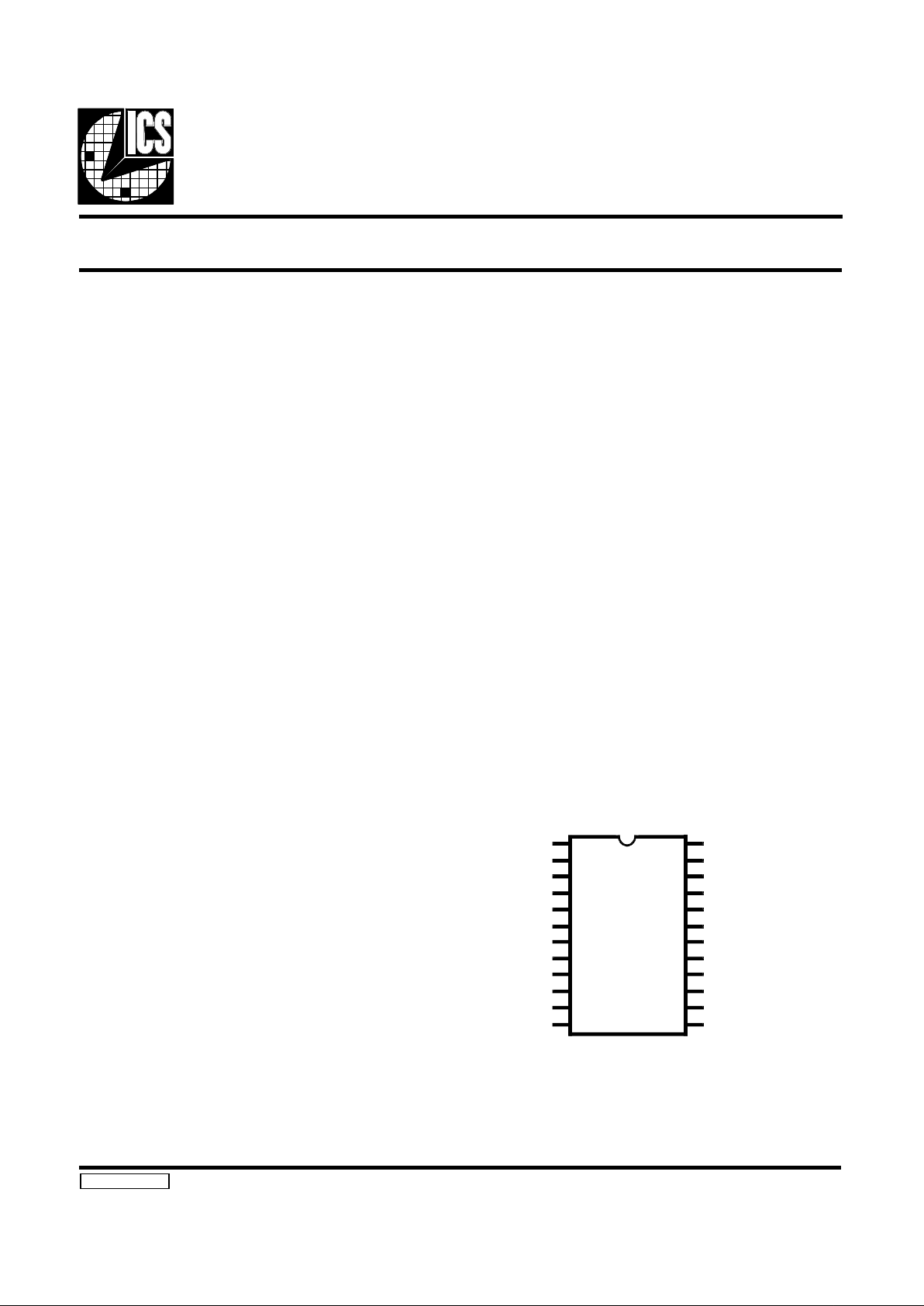
OUT2 1 24 OUT3
OUT1 2 23 OUT4
OUT0 3 22 OUT5
OUT9 4 21 OUT6
CPUCLK 5 20 OUT7
(CPUCLK/2)
VSS 6 19 OUT8
DVDD 7 18 A VDD
STROBE 8 17 XTAL2
CPUSEL0 9 16 XTAL1
CPUSEL1 10 15 A VSS
CPUSEL2 11 1 4 OUTPUTE
CPUSEL3 12 13 CLKIN
24-Pin DIP or SOIC
ICS2694
Pin Configuration
ICS2694RevA1094
Applications
•• CPU clock and Co-processor c lock
•• Hard Disk and Floppy Disk cloc k
•• Keyboard clock
•• Serial Port clock
•• Bus clock
•• System count ing or timing fu nc tions

Pin Description
PIN NUMBER NAME DESCRIPTION
1 OUT2 4mA Output.
2 OUT1 4mA Output.
3 OUT0 4mA Output
4 OUT9 4mA Output.
5 CPUCLK 4mA Output driv en by Vo ltag e Controlle d Oscillat or 1 (VC01). VC01 is cont rolled
by a 16 word ROM.
6 VSS Ground for digital po rtion of chip.
7 DVDD Plus supply for digital portion of chip.
8 STROBE Input control for transparent latches a ssoc iat ed wit h CPU ( 0-3) which se lec t one of
16 values for CPUCL K. Holding ST ROBE high ca uses the latc hes to be transparent.
9 CPUSEL0 LSB CPUCLK address bit.
10 CPUSEL1 CPUCLK ad dres s bit.
11 CPUSEL2 CPUCL K ad dres s bit.
12 CPUSEL3 MSB CPUCLK ad dres s bit.
13 CLKIN An altern ative input for the ref erence c lock. The crystal osci llator out put and CLKIN
are gated togethe r to genera t e the ref er ence cl oc k for the VCO’s. If CLKIN is u sed,
XTAL1 should be held high and XTAL 2 lef t open . If the inter nal oscil lat or is used,
hold CLKIN high.
14 OUTPUTE Pulling this line low trista tes al l outpu ts.
15 AVS S Ground for analo g port io n of chip .
16 XTAL1 Input of intern al cr ysta l oscil lat or sta ge .
17 XTAL2 Output of internal crystal oscillator stage. This pin should have nothing connected
to it but one of the quar tz crystal termina ls.
18 AVD D Positive supply for analog portion of chip.
19 OUT8 4mA Output.
20 OUT7 4mA Out put . (Usually assigne d a s CPUCLK/ 2 for co-processor use.)
21 OUT6 4mA Output.
22 OUT5 4mA Output.
23 OUT4 4mA Output.
24 OUT3 4mA Output.
ICS2694
2
Frequency Reference
The internal reference oscillator contains all of the passive
components required. An appropriate series-resonant crystal
should be connected between XTAL1 (1) and XTAL2 (2). In
IBM-compatible applications, this will typically be a
14.31818 MHz crystal, but fundamental mode crystals between 10 MHz and 25 MHz have been tested. Maintain short
lead lengths between the crystal and the ICS2694. In order to
optimize the quality of the quartz crystal oscillator, the input
switching threshold of XTAL1 is VDD/2 rather than the conventiona l 1.4V of TTL. Therefore, XTAL1 may not respond
properly to a legal TTL signal since TTL is not required to
exceed VDD/2. Theref ore, another clock input CLKIN (pin 13)
has been added to the chip which is sized to have an input
switching point of 1.4V. Inside the chip, these two inputs are
ANDED. Therefore, when using the XTAL1 and XTAL2,
CLKIN should be held high. (It has a pull-up.) When using
CLKIN, XTAL1 should be held high. (It does not have a
pull-up because a pull-up would interfere with the oscillator
bias.)
It is anticipated that some applications will use both clock
inputs, properly gated, for either board test or unique system
functio ns. By gene rating all the system cl ocks from one reference input, the phase and delay relationships between the
various outp uts wil l rem a in re lat iv el y fi xe d, the re by e lim ina t ing problems ari sing from totally u nsynchroniz ed clock s interacting in a system.
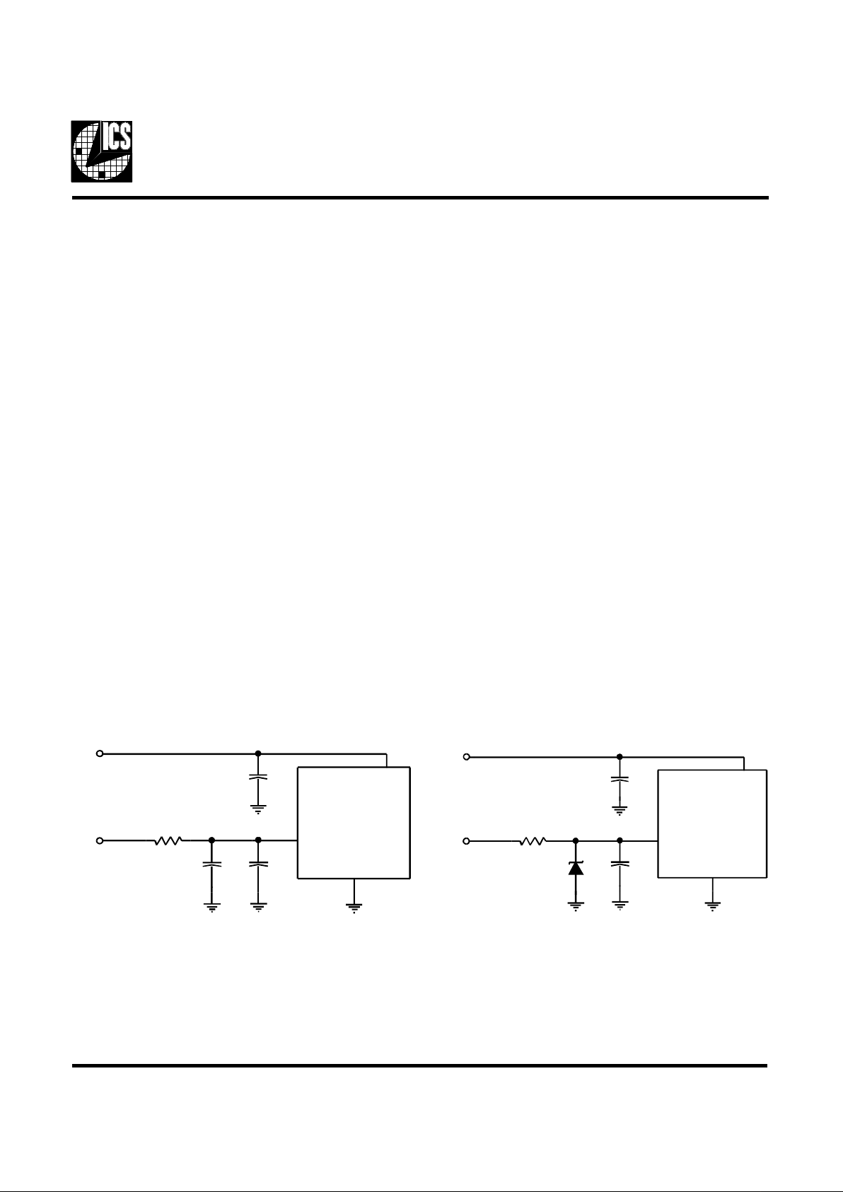
Power Supply Conditioning
The ICS2694 is a membe r of the sec ond ge nerat ion of dot cl ock
products. By inc orp orating the loop fi lte r on chi p and upgr ad ing the VCO, the ease of application has been substantially
improved o ver earl ier produc ts. If a stable and noise-fre e power
supply is availa ble, no extern al componen ts are required. However , in some appl ica ti ons it may be jud icio us to de couple the
power supply as shown in Figure s 1 or 2. Figure 1 is the normal
configuration for 5 volt only applications. Which of the two
provid es sup erior perfo rm ance d epen ds on the noise conte nt of
the power supplie s. In gene ral , the confi guratio n of Figure 1 is
satisfactory. Figure 2 is the more conventional if a 12 volt
analog suppl y is available, althoug h the improved perfor mance
comes at a c ost of an extr a compo nent; ho wever , the cost of the
discretes used i n Figure 1’s are le ss than the co st of Fig ure 1’s
discre t e components.
Since the ICS2694 outputs a large number of high-frequency
clocks, conservative design practices are recommended. Care
should be exercised in the board layout of supply and ground
traces, an d adequate power sup ply dec oupl ing c apa c itors c on sistent with the application shoul d be used .
R1
33
+5
+5
DVDD
VSS, A VSS
AVDD
C2
22µV
C1
C3
.µ1F
.µ1F
Figure 1
D1R1
470
+120
+50
DVDD
VSS, AVSS
AVDD
4.7V
C1
C2
.µ1F
.µ1F
Figure 2
ICS2694
3

Absolute Maximum Ratings
Supply Voltage . . . . . . . . . . . . . . . . VDD. . . . . . . . . . . . -0 . 5V to +7V
Input Voltage. . . . . . . . . . . . . . . . . . V
IN
. . . . . . . . . . . . -0.5V to VDD +0.5V
Output Voltage . . . . . . . . . . . . . . . . VOUT. . . . . . . . . . -0.5V to VDD +0.5V
Clamp Diod e Curre nt . . . . . . . . . . . V
IK
& IOK. . . . . . . ±30mA
Output Current per Pin . . . . . . . . . . I
OUT
. . . . . . . . . . . ±50mA
Operating Temperature . . . . . . . . . . T
O
. . . . . . . . . . . . . 0°C to + 150°C
St orage Tempera ture. . . . . . . . . . . . T
S
. . . . . . . . . . . . . -85°C to + 150°C
Power Dissipation. . . . . . . . . . . . . . P
D
. . . . . . . . . . . . . 500mW
Values beyond these ratings may damage the device. This device contains circuitry to protect the inputs and outputs against
damage due to high static voltages or elec tric fields; howe ver , it is advised that norma l precaution s be taken to avoid applic ations
of any voltage highe r than the maximum rated voltage s. For proper operation, it is recomme nded that V
IN
and V
OUT
be constra ined
to > = V
SS
and < = VDD.
PARAMETER SYMBOL CONDITIONS MIN MAX UNITS
Operating Voltage Range V
DD
4.0 5.5 V
Input Low Voltage V
IL
VDD = 5V VSS 0.8 V
Input High Voltage V
IH
VDD = 5V 2.0 V
DD
V
Input Leakage Curre nt I
IH
VIN = V
cc
-10uA
Output Low Voltage V
OL
IOL = 4.0 mA - 0.4 V
Output High Voltage V
OH
IOH = 4.0 mA 2.4 - V
Supply Current I
DD
VDD = 5V, CPUCLK = 80 MHz - 55 mA
Internal Pul l-u p Resistor s R
UP
*VDD = 5V, V
in
= 0V 50 - k ohm
Input Pin Capacitanc e C
in
Fc = 1 MHz - 8 pF
Output Pin Capacitanc e C
out
Fc = 1 MHz - 12 pF
* The followin g inputs have pul l-ups: OUTPUTE, STROBE, CPUSEL (0-3), CLKIN.
DC Characteristics (0°C to 70°C)
ICS2694
4

AC Timing Characteristics
The following notes appl y to al l para m et e rs pre se nt e d in this sec t ion :
1. Xtal Frequency = 14.31818 MHz
2. All units are in na noseconds (ns).
3. Rise and fall time is between 0.8 and 2.0 VDC.
4. Output pin loading = 15pF
5. Duty cycle is measured at 1.4V.
6. Sup p ly Voltage Range = 4.5 to 5.5 vo lts
7. Temperature Range = 0°C to 70°C
SYMBOL PARAMETER MIN MAX NOTES
STROBE TIMING
Tpw
Tsu
Thd
Strobe Pul se Width
Setup Time Data to Strobe
Hold Tim e Data to Strobe
20
10
10
-
-
-
FOUT TIMI N G
Tr
Tf
-
-
Rise T im e
Fall Time
Frequency E rro r
Maximum Frequency
-
-
3
3
0.5
135
Duty Cycle 40% min. to 60% max.
at 80 MHz
%
MHz
Note:
Pattern -004 has rising edges of CPUCLK and CPUCLK/ 2 mat ched to ± 2 ns.
STROBE
CPUSEL (0-3)
Tpw
Tsu Thd
ICS2694
5

24-Pin DIP Package
Ordering Information
ICS2694N-XXX
Example:
ICS XXXX M -XXX
Pattern Number (2 or 3 digit number for parts with ROM code patterns)
Package Type
N=DIP (Plastic)
Device Type (cons i sts of 3 or 4 digi t num be rs )
Prefix
ICS, AV=Standard Device; GSP=Genlock Device
ICS2694
6

LEAD COUNT 14L 16L 18L 20L 24L 28L 32L
DIMENSION L 0.354 0.404 0.454 0.504 0.604 0.704 0.804
SOIC Packages
Ordering Information
ICS2694M-XXX
Example:
ICS XXXX M -XXX
Pattern Number (2 or 3 digit number for parts with ROM code patterns)
Package Type
M=SOIC
Device Type (cons i sts of 3 or 4 digi t num be rs )
Prefix
ICS, AV=Standard Device; GSP=Genlock Device
ICS2694
7

ICS2694 Standard Patterns
CPUSEL0-3
(Hex)
CPUCLK OUTPUT (Pin 5)
(MHz)
02
110
220
324
425
532
6 33.33
740
848
950
10 54
11 66.67
12 68
13 80
14 100
15 16
Note: Pattern -004 has rising edges of CPUCLK and
CPUCLK/2 match ed to ± 2 ns.
Another alternative for CPU CLOCK generation is the
ICS2494-244 if the additional functions of the ICS2694 are
not need ed in th e appl ic a ti on.
ICS
Part Number
ICS2494-
244
Address FS3-0
(Hex)
Frequenc y
(MHz)
020
124
232
340
450
566.6
680
7 100
854
970
090
B110
C25
D33.3
E40
F50
Addre ss MS1-0
(Hex)
Frequency
(MHz)
016
124
250
366.6
32 MHz 1 24 16 MHz
.846 MHz 2 23 8 MHz
24 MHz 3 22 9.6 MHz
6 MHz 4 21 14.318 MHz
CPUCLK 5 20 CPUCLK/2
VSS 6 19 1.19 MHz
DVDD 7 18 AVDD
STROBE 8 17 XTAL2
PUSEL0 9 16 XTAL1
PUSEL1 10 15 AVSS
PUSEL2 11 14 OUTPUTE
PUSEL3 12 13 CLKIN
ICS2694-004
ICS2694
8
 Loading...