

Integrated
ICS157 2
Circuit
Systems, Inc.
User Programmable Differential Output Graphics Clock Generator
Description
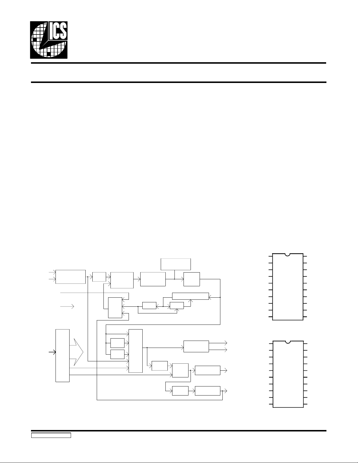
The ICS1572 is a high performance monolithic phase-locked
loop (PLL) frequency synthesizer. Utilizing ICS’s advanced
CMOS mixed-mode technology, the ICS1572 provide s a low
cost solution for high-end video clock generation in workstations and high-e nd PC applicat ion s.
The ICS1572 has differential video clock outputs (CLK+ and
CLK-) that are compat ible with industry standard vide o DACs.
Another clo ck output , LOAD, is p rovi de d wh ose frequency is
derived from the main clock by a programmable divider. An
additional clock output is available, LD/N2, which is derived
from the LOAD frequency and whose modulus may also be
programmed.
Operati ng frequenc ies are fully progra mmable with direct con trol provi ded for refe rence div ider , pre-scale r, fee dback divi der
and post-sca ler.
Reset of the pipeline delay on Brooktree RAMDACs may
be performed under register control. Outputs may also be set
to desired states to facilitate circuit board testing.
XTAL1
XTAL2
EXTFBK
BLANK
CRYSTAL
OSCILLATOR
(-301 only)
PROGRAMMIN G
INTERFACE
/ R
PHASE-
FREQUENCY
DETECTOR
MUX
/ 2
/ 4
MUX
CHARGE
PUMP
/ M
FILTER
/ N1
Features
• Supports high-resolution graphics - CLK output to
180 MHz
Eliminate s nee d for mul tiple ECL o utput cr ysta l osci lla tors
•
• Fully programmable synthesizer capability - not just a
cloc k mu ltiplier
• Available in 20-pin 300 -m il wi de body SOIC package
• Available in both parallel (101) and serial (301)
programming versions
• Circuit incl uded for reset of Brooktr ee RAMDAC pipeline
delay
Applications
• Workstations
• AutoCad Accelerators
• High-end PC graphics syst ems
ICS1572-101 Pinout
LOOP
VCO
PRESCALER
/ A
FEEDBACK DIVIDER
DIFF.
OUTPUT
MUX DRIVER
/ N2
DRIVER
CLK+
CLK−
LOAD
LD/N2
N.C. 1 20 N.C.
AD0 2 19 AD1
XTAL1 3 18 AD2
XTAL2 4 17 VDD
STROBE 5 16 VDD
VSS 6 15 VDDO
VSS 7 14 IPRG
LOAD 8 13 CLK+
LD/N2 9 12 CLK-
N.C. 10 11 N.C.
ICS1572-301 Pinout
N.C. 1 20 N.C.
AD0 2 19 AD1
XTAL1 3 18 AD2
XTAL2 4 17 VDD
STROBE 5 16 VDD
VSS 6 15 VDDO
VSS 7 14 IPRG
LOAD 8 13 CLK+
LD/N2 9 12 CLK-
N.C. 10 11 N.C.
ICS1572RevC093094
Figure 1
RAMDAC is a trademark of Brooktree Corporation.

ICS1572
Overview
The ICS1572 is ideally suited to provide the graphics system
clock signals required by high-performance video DACs.
Fully pr ogra m mab le fe ed ba ck an d r ef er en ce di vi der c ap abil it y
allow virtually any frequency to be generated, not just simple
multiples of the reference frequency. The ICS1572 uses the
latest genera tion of fre quency synthesis techni ques developed
by ICS and is completely suitable for the most demanding
video applic at io n s.
PLL Synthesizer Description Ratiometric Mode
The ICS1572 generates its output frequencies using phaselocked loop techniques. The phase-locked loop (or PLL) is a
closed-loop feedback system that drives the output frequency
to be ratiometrically related to the reference frequency provided to the PLL (see Figure 1). The reference frequency is
generated by an on-chip crystal oscillator or the reference
frequency may be applied to the ICS1572 from an external
frequency source.
The phase-frequency detector shown in the block diagram
drives the voltage-c ontrolled o scillator , or VCO, to a freq uency
that will cause the two inputs to the phase-frequency detector
to be matc hed in fre que ncy and pha se. This oc curs whe n:
PLL Post-Scaler
A p rogrammable po st-scaler may be inserted b etween the VCO
and the CLK+ a nd CLK- outputs of the ICS1572. T his is useful
in generating of lower frequencies, as the VCO has been
optimize d for hig h-fr eq ue nc y ope ra tion.
The post-scaler allows the selection of:
• VCO frequenc y
• VCO frequenc y di vided by 2
• VCO frequenc y di vided by 4
• Internal regi ster bit (AUXCL K) va lu e
Load Clock Divider
The ICS1572 has an additional programmable divider
(referred to in Figure 1 as the N1 divider) that is used to
generate the LOAD clock frequency for the video DAC. The
modulus of th is div ide r m a y be set to 3, 4, 5, 6, 8, or 10 un de r
register control. The design of this divider permits the output
duty factor t o be 50/50, even when an odd mod ulus is selecte d.
The input frequency to this divider is the output of the PLL
post-scaler described above.
F(
VCO)
This expression is exact; that is, the accuracy of the output
frequen cy depe nds solel y on the re fere nce freq uenc y provi de d
to the part (assuming correctly programmed dividers).
The VCO gain is programmable, which permits the ICS1572 to
be optimized for best performance at all operating frequencies.
The reference divider may be programmed for any modulus
from 1 to 128 in steps of one.
The feedback divider may be programmed for any modulus
from 37 through 391 in ste ps of one . Any e ve n modul us from
392 through 782 can also be achieved by setting the “double”
bit whic h double s the feed back divid er m odulus. The fe edba ck
divider makes use of a dual-modulus prescaler technique that
allows the programmable counters to operate at low speed
without sacrificing resolution. This is an improvement over
conventional fixed prescaler architectures that typically impose a factor-of- four penal ty (or lar ger) in this respect .
T able 1 permits the derivat ion of “A” & “M” count er progra mming dire c tl y fr o m de sired mod ulu s.
F(XTAL1) . Feed back Divider
: =
Refe rence Divider
Digital Inputs - ICS1572-101 Option
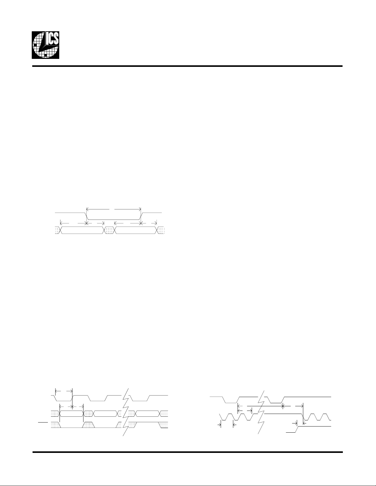
The AD0-AD3 pins and the STROBE pin are used to load all
control regi ste rs of t he ICS1572 (-101 option). The AD0-A D3
and STROBE pins are each equipped with a pull-up and will
be at a logic HIGH level when not connected. They may be
driven with sta nda rd TTL or CMOS logic fam il ies.
The address of the register to be loaded is latched from the
AD0-AD3 pins by a negative edge on the STROBE pin. The
data for that register is latched from the AD0-AD3 pins by a
positive edge on the STROBE pin. See Figure 2 for a timing
diagram. Aft e r power-up, th e ICS1572-101 requires 32 regis-
ter writes for new programming to become effective. Since
only 13 re gisters are used at present, the program m ing system
can perform 19 “dummy” writes to address 13 or 14 to comple te th e s eq uence.
2
ICS157 2
This allows the synthesizer to be comple tel y progr am m e d for
the desired frequency before it is made active. Once the part
has been “unlo ck ed ” by the 32 wri tes, progr am m in g beco me s
effe ct ive imme di at e ly.
ALL registers identified in the data sheet (0-9, 11, 12 & 15)
MUST be written upon initial progra mming. The programming
registers are not initialized upon power-up, but the latched
outputs of those registers are. The latch is made transparent
after 32 re gister wr ites. If any register ha s not been wri tten, the
state up on power- up (random ) will be come ef fective . Registe rs
13 & 14 physically do not exist. Regi ste r 10 doe s exi st, but is
reserved for future expansion. To insure compatibility with
possible futur e modific ations to the database, ICS recom mends
that all three unused loc ati ons be writte n with ze ro.
ICS1572-101 Register Loading
STROBE
1
AD0-AD3
5
2
3
DATA VALIDADDRESS VALID
4
Figure 2
An additional control pin on the ICS1572-301, BLANK can
perform either of two functions. It may be used to disable the
phase-fre qu ency detect or in line -l ocke d appli cat ions. Alt erna tively, the BLANK pin may be used as a synchronous enable
for VRAM shift clock genera tion. See sections on Line -Locked
Operations and VRAM shif t clock gen er atio n for deta ils.
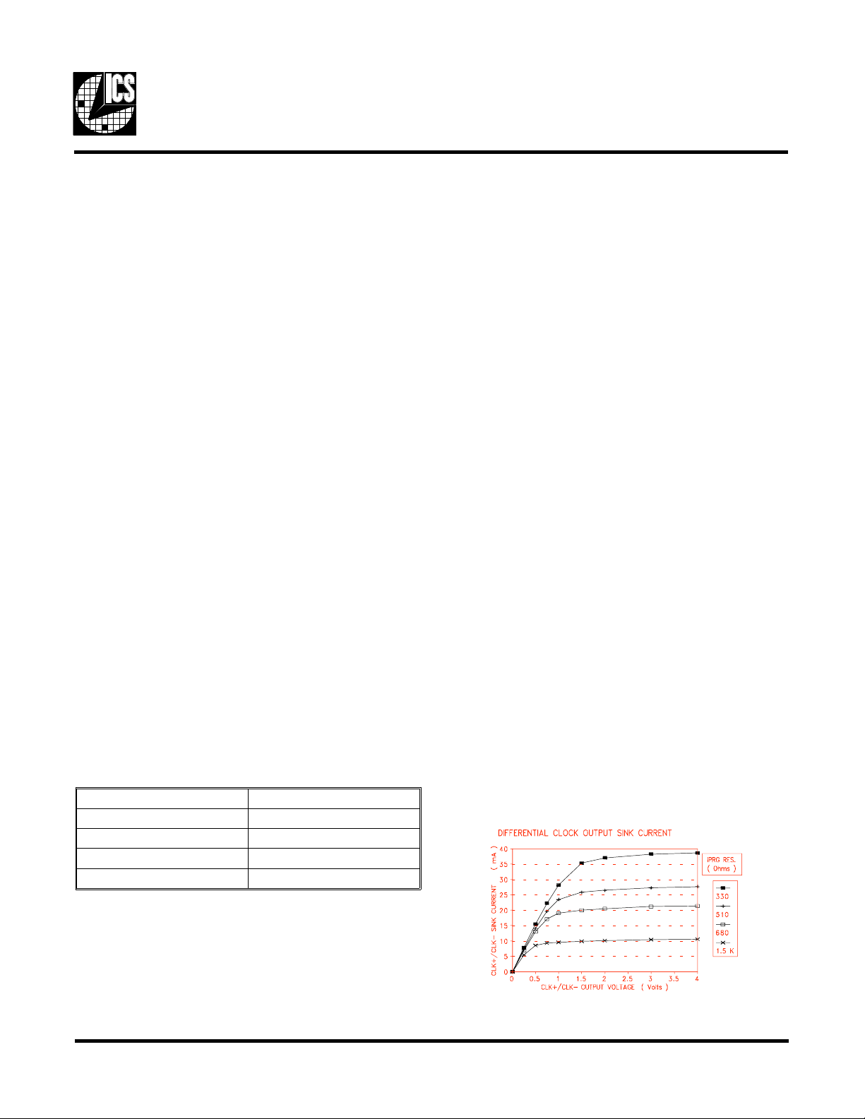
Output Description
The differential output drivers, CLK+ and CLK, are currentmode and are designed to drive resistive terminations in a
comple mentary fashion. The outputs are current-sinking only,
with the amount of sink current programmable via the IPRG
pin. Th e sink c urren t, which is steere d to eit her CLK + or CL K-,
is approximately four times the current supplied to the IPRG
pin. For mo st applica tions, a re sistor from VDDO to IPRG wi ll
set the current to the necessary precision. See Figure 6 for
output characteristic s.
The LOAD output is a high-current CMOS type drive whose
frequen cy is controlled by a programmable di vider that may be
selected for a modulus of 3, 4, 5, 6, 8, or 10. It may also be
suppressed under re gi ste r cont rol .
The LD/N2 output is high-current CMOS type drive whose
frequen cy is derive d from the L OAD output . The progr amma ble modulus m ay range from 1 to 512 in steps of on e.
Digital Inputs - ICS1572-301 Option
The programming of the ICS1572-301 is performed serially
by using the DATCLK, DATA, and HOLD~pins to load an
internal shift register.
DATA is shifted into the register on the rising edge of
DATCLK. T he log ic value on the HOL D~ pin i s latc he d at the
same time. When HOLD~ is low, the shift register may be
loaded witho ut di sturbing the op eratio n of the ICS1572. When
high, the shift register outputs are transferred to the control
registers, and the new programming information becomes active. Ordina rily, a high level should be place d on the HOLD~
pin when the last data bit is presented. See Figure 3 for the
program mi ng se que nc e .
ICS1572-301 Register Loading
8
DATCLK
67
DATA
HOLD
DATA_1 DATA_2 DATA_56
Figure 3
Pipeline Delay Reset Function
The ICS1572 implements the clocking sequence required to
reset the pipeline delay on Brooktree RAMDACs. This sequence can be generated by setting the appropriate register bit
(DACRST) to a logic 1 and then resetting to logic 0.
When changing frequencies, it is advisable to allow 500 microseconds after the new frequency is selected to activate the
reset function. The output fr equency of the sy nthesiz e r should
be stable enough at that point for the video DAC to correctly
execute its reset sequence. See Figure 4 for a diagram of the
pipeline delay reset sequence.
Pipeline Delay Reset Timing
STROBE
or
DATCLK
CLK+
LOAD
10
9
T
CLK
11
12
Figure 4
3

ICS1572
Reference Oscillator and Crystal
Selection
The ICS1572 has circuitry on-board to implement a Pierce
oscilla tor with the ad dit ion of only one extern al component, a
quartz crystal. Pierce oscillators operate the crystal in anti(also called parallel-) resonant mode. See the AC Characteristics for the effective capacitive loading to specify when
orde ri n g cr ystal s .
Series-resonant crystals may also be used with the ICS1572.
Be aware that the oscillation frequency wil l be slight ly higher
than the frequency that is stamped on the can (typically 0.025-
0.05%).
As t he e nt ire op erat io n o f the ph ase -lo ck ed l oop d epen ds on
havin g a st able re ferenc e freq uency, we rec ommend that the
crystal be mo unted as c losel y as p ossibl e to the pa cka ge. Avoid
routing digital signals or the ICS1572 outputs underneath or
near these traces. It is also desirable to ground the crystal can
to the ground plane, if possible.
If an exte rnal re fere nce fr eque ncy sour ce is to be used wit h the
ICS1572, it is important that it be jitter-free. The rising and
falling edges of that signa l shou ld be f ast and f re e of n oise fo r
best result s.
ICS1572-101 The ICS1572-101 supports phase detector
disable via a special control mode. When the
PDRSTEN (phase dete ctor rese t enable) bit is
set, a high level on AD3 will disable PLL
locking.
ICS1572-301 The ICS1572-301 supports phase detector
disable via the BLANK pin. When the
PDRSTEN bit is set, a high level on the
BLANK input will disa ble PL L locking.
External Feedback Operation
The ICS1572-301 option also supports the inclusion of an
extern al co unter as the feed back divide r o f the PL L. This m ode
is useful in graphic systems that must be “genlocked” to
external video sourc es.
When the EXT FBE N bi t is set to logi c 1, the ph ase -fr eq ue ncy
detector will use the EXTFBK pin as its feedback input. The
loop phase will be locked to the rising edges of the signal
applied to the EXT FBK i nput .
VRAM Shift Clock Generation
The loop phase is locked to the falling edges of the XTAL1
input signals.
Line-Locked Operation
The ICS1572 supports line-locked clock applications by allowing the LOAD (N1) and N2 divider chains to act as the
feedba c k div ide r fo r the PL L.
The N1 and N2 d ivide r cha ins allow a much l arg er modul us to
be achieved than the PLL ’ s own feedback divide r. Additionall y,
the output of the N2 counter is ac cessible off-c hip for perfo rming horizontal reset of the graphics system, where necessary.
This mode is set under register control (ALTLOOP bit). The
refere nc e di vid er (R counter) i s set to di vid e by 1 in this m ode ,
and the HSYNC signal of the external video will be supplied
to the XTAL1 input. The output frequency of the synthesizer
wil l t h en be:
F
: = F (XTAL1) . N1 . N2.
(CLK)
By using the phase-detector hardware disable mode, the PLL
can be ma de to fre e- run a t the be gin ning o f the v er tica l i n t e r v a l
of the external video, and ca n be reactivated at its com ple tion.
The ICS1572-301 option supports VRAM shift clock generation and interruption. B y programmin g the N2 c ounter to d ivide
by 1, the LD/N2 output becomes a duplicate of the LOAD
output. When the SCEN bit is set, the LD/N2 output may be
synchronously started and stopped via the blank pin. When
BLANK is high, the LD/ N2 wil l be free -run ning and in phase
with LOAD. When BLANK is take n low , the LD/N2 out put is
stopped at a low level. See Figure 5 for a diagram of the
sequence. Note that this use of the BLANK pin precludes its use
for phase comparator disable (see Line-Locked O peration).
VRAM Shift Clock Control
BLANK
LOAD
LD/N2
Figure 5
4
ICS157 2
Power-On Initialization
The ICS1572 has an internal power-on reset circuit that performs the followin g func t ion s:
1) Sets the mu lt ipl e xe r to pass the re ferenc e fr equenc y
to the CLK+ and CL K- outputs.
2) Selects the mo dul us of the N1 di vid er (for the
LOAD clock) to be four .
These functions should allow initialization of most graphics
systems that can not imme diately provide fo r register pro gramming upon system power-up.
Because the power -o n reset circ uit is on the VDD supply, and
because that supply is filte red, ca re must be take n to allow the
reset to de-assert before programming. A safe guideline is to
allow 20 microse c onds a fter t he VDD supp ly reac he s 4 vol ts.
Programming Notes
• VCO Frequency Range: Use the post-divider to keep the
VCO frequency as high as possible within its operating
range.
• Divider Range: For best results in normal situatio ns (i.e.,
pixel cloc k ge nera tion for hi-res displ ay s), kee p the refe rence di vide r m odulu s as short a s p ossibl e (f or a fre que ncy
at the output of the reference divider in the few hundred
kHz to several MHz range) . If you need to go to a lower
phase comparator reference frequency (usually required
for increa sed frequ ency accura cy), that is acceptab le, but
jitter perfo rman ce wil l suffer some wha t.
• VCO Gain Programming: Use the minimum gain which
can relia bly achi eve t he VCO fre quen cy desi red, as shown
here:
VCO GAIN MAX FREQUENCY
4 120 MHz
5 200 MHz
6 230 MHz
7*
* SPECIAL APPLICATION. Contact factory for custom product above
230 MHz.
• Phase Detector Gain: For most graph ics appl ica tions and
divider ranges, set P[1,0] = 10 and set P[2] = 1. Under
some circumstances, setting the P[2] bit “on” can reduce
jitter. During 1572 operation at exact multiples of the
crystal frequency, P[2] bit = 0 may provide the best jitter
performance.
Board Test Support
It is often desi rabl e to statica lly contr ol the leve ls of the output
pins for ci rc ui t b oa rd t e st . T he ICS1572 supports this through
a register programmable mode, AUXEN. When this mode is
set, two register bits directly control the logic levels of the
CLK+/CLK- pins and the LOAD pin. This mode is activated
when the S[0] and S[1] bits are both set to logi c 1. See Registe r
Mapping for deta il s.
Power Supplies and Decoupling
The ICS1572 has two VSS pins to reduc e the effe cts of package
inductance. Both pins are connected to the same potential on
the die (the ground bus). BOTH of these pins should connect
to the ground plan e of the video board a s close to the package
as is po ssible.
The ICS1572 has a VDDO pin which is the supply of +5 volt
power to all output drive rs. This pin should be connect ed to the
power plane (or bus) using standard high-frequency decoupling pra ctice. T hat is, ca pacitors should hav e low seri es induc tance an d be mounte d c lo se to the ICS1572.
The VDD pin is the power suppl y pin for the PLL synthesizer
circuitry and ot her lower c urrent digital functions. We recom mend that RC decoupling or zener regulation be provided for
this pin (as sh own in the recommen ded application ci rcuitry).
This wil l allow the PLL to “t rack” through power supply
fluctuations without visible effects. See Figure 7 for typical
external circui try.
Figure 6
5
ICS1572
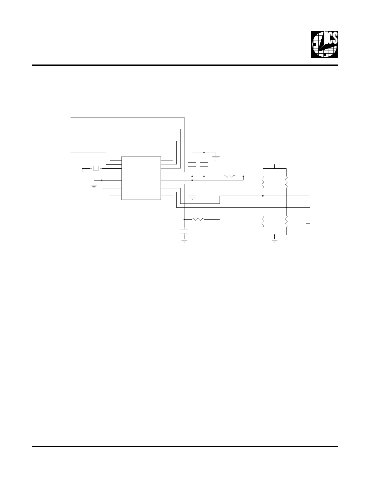
ICS1572 Typical Interface
DATA BUS
SELECT
1 N.C. N.C 20
2AD0 AD1 19
3XTAL1 AD2 18
4XTAL2 AD3 17
5 STROBE VDD 16
6 VSS VDDO 15
7 VSS IPRG 14
8LOAD CLK+ 13
9 LD/N2 CLK- 12
10 N.C. N.C. 11
Figure 3
+5V
+
120
120
390390
TO
RAMDAC
6

ICS157 2
Register Mapping - ICS1572-101 (Parallel Programming Option)
NOTE: IT IS NOT NECESSARY TO UNDERSTAND THE FUNCTION OF THESE BITS TO USE THE ICS1572. PC SOFTWARE IS AVAILABLE
FROM ICS TO AUTOMATICALLY GENERATE ALL REGISTER VALUES BASED ON REQUIREMENTS. CONTACT FACTORY FOR DETAILS.
REG# BIT(S) BIT REF. DESCRIPTION
0 0-3 R[0]..R[3] Referenc e divi de r modul us con tro l bi ts
1 0-2 R[4]..R[6] Modulus = value + 1
2 0-3 A[0]..A[3] Controls A counter. When set to zero, modulus=7. Otherwise,
modulus=7 for “ va lue ” unde rf lows of t he presc ale r, and modulus=6
thereafter until M counter underf lows.
3 0-3 M[0]..M[3] M counter control bits
4 0-1 M[4]..M[5] Modulus = value + 1
4 3 DBLFREQ Doubles modulus of dual -m odu lus pre sc al er (fro m 6/7 to 12/1 4).
5 0-2 N1[0]..N1[2] Sets N1 modulus according to this table. These bits are set to imple-
ment a divide-by-four on power -up .
N1[2] N1[1] N1[0] RATIO
0003
0014
0104
0115
1006
1018
1108
11110
6 0-3 N2[0]..N2[3] Sets the mo dulus of the N2 divider . Modulus = value + 1
7 0-3 N2[4]..N2[7] The input of the N2 divi de r is the out put of the N1 divi de r in all cloc k
modes except AUXEN.
8 3 N2[8]
8 0-2 V[0]..V[1] Sets the ga in of the VC O.
V[2] V[1] V[0] VCO GAIN
(MHz/VOLT)
100 30
101 45
110 60
111 80
7

ICS1572
REG# BIT(S) BIT REF. DESCRIPTION
9 0-1 P[0]..P[1] Sets the ga in of the phase de t ec t or a ccording to this tabl e .
P[1] P[0] GAIN (uA/radian)
00 0.05
01 0.15
10 0.5
11 1.5
9 3 [P2] Phase detecto r tuning bit. Norma lly shoul d be set to one.
11 0-1 S[0]..S[1] PLL post-sca le r/te st m ode selec t bits
S[1] S[0] DESCRIPTION
0 0 Post-scaler =1. F(CLK)=F(PL L). The output of the N1 d ivider drives
the LOAD output which, in turn , drives the N2 divid er.
0 1 Post-scaler=2. F(CLK)=F(PLL)/2. The output of the N1 divider
drives the LOAD outp ut whi ch, in turn, dri ve s the N2 divide r.
1 0 Post-scaler=4. F(CLK)=F(PLL)/4. The output of the N1 divider
drives the LOAD outp ut whi ch, in turn, dri ve s the N2 divide r.
1 1 AUXEN CLOCK MODE. The AUXCLK bit dr ives the dif fe rentia l
outputs CLK+ and CLK- and the AUXN1 bit drives the LOAD
output which, in turn, drives th e N2 di vi der.
11 2 AUX_CLK When in the AUXEN cloc k mode, this bit controls the diffe rent ial
outputs.
11 3 AUX_N1 When in the AUXEN clock mode, thi s bit contr ols t he LOAD o utp ut
(and consequently the N2 outp ut ac co rdi ng to its pro gra m ming) .
12 0 RESERVED Must be set to zero.
12 1 JAMPLL Tristate s phase detec tor outputs; resets phase de tector logic, and
12 2 DACRST Set to zero for norma l opera t ion . When set to one, th e CLK+ ou tpu t is
12 3 SELXTAL When set to logic 1, passes the ref er ence fre qu en cy to the post-scaler .
15 0 ALTLOOP Controls subst itut ion of N1 and N2 divide rs in to fee dba c k lo op of PL L .
15 3 PDRSTEN Phase-dete ctor r ese t enabl e contr ol bit . When thi s bit is set, the AD3
resets R, A, M, and N2 counters.
kept high a nd t he CLK- outp ut i s kept low . (Al l othe r de vice functions are
unaffe c te d. ) When returned to zero, the CLK+ and CLK- out put s will
resume toggl ing on a rising edge of the LD ou tpu t (+/- 1 CLK peri od) .
T o initi a te a RAMDAC reset se que nce , simpl y write a one to
this registe r bi t fo ll owe d by a zero.
When this bit is a logic 1, the N1 and N2 dividers are used.
pin becomes a transparent reset input to the phase detector.
See LINE-LOCKED CLOCK GENERATION section for more
detail s on the ope ra t ion of thi s function.
8

ICS157 2
Register Mapping - ICS1572-301 (Serial Programming Option)
NOTE: IT IS NOT NECESSARY TO UNDERSTAND THE FUNCTION OF THESE BITS TO USE THE ICS1572. PC SOFTWARE IS AVAILABLE
FROM ICS TO AUTOMATICALLY GENERATE ALL REGISTER VALUES BASED ON REQUIREMENTS. CONTACT FACTORY FOR DETAILS.
BIT(S) BIT REF. DESCRIPTION
1-3 N1[0]..N1[2] Sets N1 modulu s ac cording to thi s table. These b it s are set to impl em ent
4 RESERVED Set to zero.
5 RESERVED MUST be set to zer o. If this bit is ev er progr am me d for a logic one, devic e
6 JAMPLL Tristate s phase detector output s, re set s p ha se de te c tor logic, and resets
7 DACRST Set to zero for normal operations. Whe n set to one, the CLK+ output is
a divide-by-four on power -up .
N1[2] N1[1] N1[0] RATIO
0003
0014
0104
0115
1006
1018
1108
11110
operati on wi ll cea se a nd fur the r se rial data loa d in to t he reg iste rs wil l be
inhibited until a powe r -of f/ powe r -o n sequ ence .
R, A, M, and N2 c ounters.
kept high a nd t he CLK- outp ut i s kept low . (Al l othe r de vice functions are
unaffe c te d. ) When returned to zero, the CLK+ and CLK- out put s will
resume toggl ing on a rising edge of the LD output (+/−1 CLK peri od).
T o initi a te a RAMDAC reset se que nce , simpl y write a one to this registe r
bit followed by a zer o.
8 SELXTAL When set to logic 1, passes the refer en ce frequ en cy to the post -sc ale r.
9 ALTLOOP Controls substitut ion of N1 and N2 div iders into fee dba c k loop of PLL.
When this bit is a logic 1, the N1 and N2 dividers are used.
10 SCEN VRAM shift clock enable bit. When logic 1, the BLANK pin can be used
to disable the L D/N2 output.
11 EXTFBKEN Externa l PLL feedbac k sel ect . When logi c 1, the EX T FBK pin is used for
the phase -fre qu ency dete ctor feedback input.
12 PDRSTEN Phase detector re set enable contro l bit. When this bit is se t, a high level
on the BLANK input will disabl e PL L lo ck ing . See LINE-L OCKE D
CLOCK GENERATION section for more de tai ls on the operation of
this function.
9

ICS1572
BIT(S) BIT REF. DESCRIPTION
13-14 S[0]..S[1] PLL post-scaler/test mode select bits.
S[1] S[0] DESCRIPTION
0 0 Post-scaler= 1. F(CLK)=F(PLL ). The output of the N1 divider drive s
the LOAD output which, in turn, drive s the N2 div ider.
0 1 Post-scaler=2. F(CLK)=F(PLL)/2. The output of the N1 divider
drives the LOAD ou tpu t whi ch , in turn, driv es th e N2 divi de r.
1 0 Post-scaler=4. F(CLK)=F(PLL)/4. The output of the N1 divider
drives the LOAD ou tpu t whi ch , in turn, driv es th e N2 divi de r.
1 1 AUXEN CLOCK MODE. The AUXCL K bit dri ves the dif fere ntial
outputs CLK+ and CLK- and the AUXN1 bit drives the LOAD
output which, in turn , drives the N2 divid er.
15 AUX_CLK When in the AUXEN cl ock mode, thi s bit controls the differential ou tputs.
16 AUX_N1 When in the AUXEN clock mode , this bit contr ols t he N1 output (a nd
17-24 N2[0]..N2[7] Sets the mo dul u s of the N2 di vid er. The input of the N2 di vi de r is t he
28 N2[8] output of the N1 divider in all clock modes except AUXEN.
25-27 V[0]..V[2] Sets the ga in of VCO.
29-30 P[0]..P[1] Sets the gain of the phase de t ec t or a ccording to this tabl e .
consequentl y the N2 ou tpu t accor ding to its programmi ng).
V[2] V[1] V[0] VCO GAIN
(MHz/VOLT)
100 30
101 45
110 60
111 80
P[1] P[0] GAIN (uA/radian)
00 0.05
01 0.15
10 0.5
11 1.5
31 RESERVED Set to z ero.
32 P[2] Phase detecto r tun ing bit. Should normally be set to one.
10

ICS157 2
BIT(S) BIT REF. DESCRIPTION
33-38 M[0]..M[5] M counter control bits
Modulus = value +1
39 RESERVED Set to z ero.
40 DBLFREQ Doubles modulus of du al -m odu lus pre sc al er (fro m 6/7 to 12/1 4).
41-44 A[0]..A[3] Controls A counter. When set to zer o, modulus=7. Otherwise,
modulus=7 for “ va lue ” unde rf lows of t he presc ale r, and modulus=6
thereafter until M counter underf lows.
45-48 RESERVED Set to z ero.
49-55 R[0]..R[6] Refere nc e divide r mo dul us con tro l bits
56 RESERVED Set to z ero.
Modulus = value + 1
11

ICS1572
Table 1 - “A” & “M” Divider Programming
Feedback Divider Modul us Table
A[2]..A[0]- 001 010 011 100 101 110 111 000
M[5]..M[0]
000000 7
000001 13 14
000010 19 20 21
000011 25 26 27 28
000100 31 32 33 34 35
000101 37 38 39 40 41 42
000110 43 44 45 46 47 48 49
000111 49 50 51 52 53 54 55 56
001000 55 56 57 58 59 60 61 63
001001 61 62 63 64 65 66 67 70
001010 67 68 69 70 71 72 73 77
001011 73 74 75 76 77 78 79 84
001100 79 80 81 82 83 84 85 91
001101 85 86 87 88 89 90 91 98
001110 91 92 93 94 95 96 97 105
001111 97 98 99 100 101 102 103 112
010000 103 104 105 106 107 108 109 119
010001 109 110 111 112 113 114 115 126
010010 115 116 117 118 119 120 121 133
010011 121 122 123 124 125 126 127 140
010100 127 128 129 130 131 132 133 147
010101 133 134 135 136 137 138 139 154
010110 139 140 141 142 143 144 145 161
010111 145 146 147 148 149 150 151 168
011000 151 152 153 154 155 156 157 175
011001 157 158 159 160 161 162 163 182
011010 163 164 165 166 167 168 169 189
011011 169 170 171 172 173 174 175 196
011100 175 176 177 178 179 180 181 203
011101 181 182 183 184 185 186 187 210
011110 187 188 189 190 191 192 193 217
011111 193 194 195 196 197 198 199 224
A[2]..A[0]- 001 010 011 100 101 110 111 000
M[5]..M[0]
100000 199 200 201 202 203 204 205 231
100001 205 206 207 208 209 210 211 238
100010 211 212 213 214 215 216 217 245
100011 217 218 219 220 221 222 223 252
100100 223 224 225 226 227 228 229 259
100101 229 230 231 232 233 234 235 266
100110 235 236 237 238 239 240 241 273
100111 241 242 243 244 245 246 247 280
101000 247 248 249 250 251 252 253 287
101001 253 254 255 256 257 258 259 294
101010 259 260 261 262 263 264 265 301
101011 265 266 267 268 269 270 271 308
101100 271 272 273 274 275 276 277 315
101101 277 278 279 280 281 282 283 322
101110 283 284 285 286 287 288 289 329
101111 289 290 291 292 293 294 295 336
110000 295 296 297 298 299 300 301 343
110001 301 302 303 304 305 306 307 350
110010 307 308 309 310 311 312 313 357
110011 313 314 315 316 317 318 319 364
110100 319 320 321 322 323 324 325 371
110101 325 326 327 328 329 330 331 378
110110 331 332 333 334 335 336 337 385
110111 337 338 339 340 341 342 343 392
111000 343 344 345 346 347 348 349 399
111001 349 350 351 352 353 354 355 406
111010 355 356 357 358 359 360 361 413
111011 361 362 363 364 365 366 367 420
111100 367 368 369 370 371 372 373 427
111101 373 374 375 376 377 378 379 434
111110 379 380 381 382 383 384 385 441
111111 385 386 387 388 389 390 391 448
Notes:
To use this tab le , find the de sire d m odul us in t he ta bl e. Fol lo w the column up to fi nd t he A divider progra m ming values.
Follow the row to the left to find the M divide r programming . Some feed ba ck divisors can be ach ieve d wit h two or thr ee
combin ations of divider settings. Any a re ac ce pt able for use.
The form ul a fo r the ef fective fe e dba c k modulus is: N =[(M +1 ) . 6] +A
except when A=0, then: N=(M +1) . 7
Under all circum sta nc e s: A ≤ M
12

ICS157 2
Pin Descriptions - ICS1572-101
PIN# NAME DESCRIPTION
13 CLK+ Clock out (non-inverted)
12 CLK
8 LOAD Load outp ut. This out put is normally a t th e CLK fre quency divided by N1.
3 XT AL 1 Quartz crysta l con ne ct io n 1/e xt e rna l re fe re nc e fre que nc y i nput
4 XTAL2 Quartz crystal connection 2
2 AD0 Address/Data Bit 0 (LSB)
19 AD1 Address/Da ta Bi t 1
18 AD2 Address/Data Bit 2
17 AD3 Address/Da ta Bi t 3 (MSB)
9 LD/N2 Divided LOAD outp ut. See tex t.
5 STROBE Control for address/data latch
16 VDD PLL system power (+5V. See applicati on diagram. )
15 VDDO Output stage powe r (+5V)
14 IPRG Output stage curre nt set
6,7 VSS Device ground. Both pins must be connected to the same ground potential.
1,10,11,20 NC Not conn ect ed
− Clock out (inverted)
Pin Descriptions - ICS1572-301
PIN# NAME DESCRIPTION
13 CLK+ Clock out (non-inverted)
12 CLK
8 LOAD Load outp ut. This out put is normally a t th e CLK fre quency divided by N1.
3 XT AL 1 Quartz crysta l con ne ct io n 1/e xt e rna l re fe re nc e fre que nc y i nput
4 XTAL2 Quartz crystal connection 2
5 DATCLK Data Clock (Input)
19 DAT A Serial Regi ste r Da ta (Inp ut)
18 HOLD~
17 BLANK Blanking (Input). See Text.
9 LD/N2 Divided LOAD outp ut/shif t clock. Se e text.
2 EXTFBK External feedback connection for PLL (input). See text.
16 VDD PLL system power (+5V. See applicati on diagram. )
15 VDDO Output stage powe r (+5V)
14 IPRG Output stage curre nt set
6,7 VSS Device ground. Both pins must be conne cte d.
1,10,11,20 NC Not conn ect ed
− Clock out (inverted)
HOLD (Input)
13

ICS1572
Absolute Maximum Ratings
VDD, VDDO (measured to VSS) . . . . . . . . . . . . . . . . . . . . . . 7.0V
Digital Inputs . . . . . . . . . . . . . . . . . . . . . . . . . . . . . . . . . . . . . . V
Digital Outputs. . . . . . . . . . . . . . . . . . . . . . . . . . . . . . . . . . . . . V
Ambient Ope ra ti ng T empe ra t ure. . . . . . . . . . . . . . . . . . . . . . . -55 to 125°C
Storage Tem pe ra tur e . . . . . . . . . . . . . . . . . . . . . . . . . . . . . . . . -65 to 150 °C
Junction Te mp erat ure. . . . . . . . . . . . . . . . . . . . . . . . . . . . . . . . 175°C
Soldering Temperature. . . . . . . . . . . . . . . . . . . . . . . . . . . . . . . 260 °C
Recommended Operating Conditions
VDD, VDDO (measured to VSS) . . . . . . . . . . . . . . . . . . . . . . 4.75 to 5.25V
Operating Temperature (Ambient). . . . . . . . . . . . . . . . . . . . . . 0 to 70°C
DC Characteristics
TTL-Compatible Inputs
101 Option - (AD0-AD3, STROBE),
301 Option - (DATCLK, DATA,
HOLD, BLANK, EXT F BK )
-0.5 to VDD + 0.5V
SS
-0.5 to V
SS
DDO
+ 0.5V
PARAMETER SYMBOL CONDITIONS MIN MAX UNITS
Input High Voltage V
Input Low Voltage V
Input High Current I
Input Low Current I
Input Capacitan ce C
ih
il
ih
il
in
Vih =VDD - 10 uA
Vil =0.0 - 150 uA
2.0 VDD+0.5 V
VSS-0.5 0.8 V
-8pF
XT AL 1 In put
PARAMETER SYMBOL CONDITIONS MIN MAX UNITS
Input High Voltage V
Input Low Voltage V
xh
xl
3.75 VDD+0.5 V
VSS-0.5 1.25
CLK+, CLK- Outputs
PARAMETER SYMBOL CONDITIONS MIN MAX UNITS
Differentia l Output Voltage 0.6 - V
LOAD, LD/N2 Outputs
PARAMETER SYMBOL CONDITIONS MIN MAX UNITS
Output High Voltage (Ioh=4.0m A) 2.4 - V
Output Low Voltage (Iol= 8. 0mA ) - 0.4 V
14

ICS157 2
AC Characteristics
SYMBOL PARAMETER MIN TYP MAX UNITS
F
vco
F
xtal
C
par
F
load
T
xhi
T
xlo
T
high
J
clk
T
lock
I
dd
I
ddo
1 Address Setup Time 10 ns
2 Address Hold Time 10 ns
3 Data Setup Time 10 ns
4 Data Hold Time 10 ns
5 STROBE Pulse Width (T
6 DAT A/HOL D~Set up T ime 10 ns
7 DATA/HOLD~Hold Time 10 ns
8 DATCLK Pulse Width (T
9 Reset Act ivatio n Time 2*T cl k ns
10 Reset Durat io n 4*Tload ns
11 Restart Dela y 2*Tloa d ns
12 Restart Matching -1*Tclk +1.5*Tclk ns
13 CLK+/CLK- Clock Rate 180 MHz
14 LOAD To LD/N2 Skew (Sh ift Cloc k Mode) -2 0 +2 ns
VCO Frequency (see Note 1) 20 160 MHz
Crystal Frequency 5 20 MHz
Crystal Oscil la tor L oa ding Capaci tance 20 pF
LOAD Frequenc y 80 MHz
XTAL1 High Time (when dr ive n exte rna ll y) 8 ns
XTAL1 Low TIme (when driv en ex terna l ly) 8 ns
Differential Clock Output Duty Cycle
45 55 %
(see Note 2)
Differential Clock Output Cumulative
<0.06 pixel
Jitter (see Note 3)
PLL Acquire T ime (to within 1%) 500
VDD Supply Current 15 t.b.d. mA
VDDO Supply Current (excluding CLK+/-
20 t.b.d. mA
termination)
DIGITAL INPUTS - ICS1572-101
or Tlo)20 ns
hi
DIGITAL OUTPUTS - ICS1572-301
or Tlo)20 ns
hi
PIPELINE DELAY RESET
DIGITAL OUTPUTS
µs
Note 1: Use of the post-div ider is required for fre quencies lower than 20 MHz on CLK+ & CLK- output s. Use of the post-divi der
is recommended for output frequencies lower than 65 MHz.
Note 2: Using load circuit of Figure 6. Duty cycl e mea sure d at zero crossing s of dif fe re nce volt age betwe en CLK+ and CLK-.
Note 3: Cumulative jitter is define d as the maxim um error (in the t ime dom ain) of any CL K edg e, at any po int in time , com pared
with the e qui valent edge gener at e d by a n ide a l fr equency source .
ICS labora tor y te stin g indi c at e s that the ty pic a l va l ue shown ab ove can be trea t ed as a ma xim um ji tte r sp ec i fic a ti on i n
virtually all applications. Jitter performance can depend somewhat on circuit board layout, decoupling, and register
programming.
15

ICS1572
NOTES
16

ICS1572 Applicatio n I nfo rmation
Output Circuit Considerations for the ICS1572
Output Circuitry
The dot cloc k signal s CLK and CL K- are typical ly the highe st
frequency signals present in the workstation. To minimize
problems with EMI, crosstalk, and capacitive loading extra
care sh oul d b e t aken in lay in g ou t this a rea of th e P C bo ard .
The ICS1572 is packaged in a 0.3”-wide 20-p in SOIC package.
This permi ts the clock generator, crystal, and related components to be lai d ou t in a n are a t he siz e of a p osta ge sta m p. The
ICS1572 should be placed as close as possible to the RAMDAC. The CLK and CLK- pins are running at VHF frequencies; one should minimize the length of PCB trace connecting
them to the RAMDAC so that they don’t become radiators of
RF energy.
At the fr equencies that th e ICS1572 is capa ble o f, PC board
traces may be long enough to be a significant portion of a
wavelength of that frequency. PC traces for CLK and CLKshould be tre ated as transm ission lines, not just interc onnecting
wires. T hese l ines can take two f orms: m icrostri p and stripl ine.
A mic ro stri p li ne is shown be low:
Stripl ine i s the ot he r form a PC B tran smi ssion l ine can ta ke. A
buried trac e betwee n ground plan es (or betwee n a power plane
and a ground plane ) i s comm on in multi -l ay er boards.
Attempting to create a workstation design without the use of
multi-layer boards would be adventurous to say the least, the
issue would more likely be whether to place the interconnect
on the surface or between layers. The between layer approach
would work bette r from an EMI standpoint, but would be more
difficul t to lay out . A stripline is shown below:
Using 1oz. copper (0.0015” thick) and 0.040” thickness G10,
a 0.010” trace will exhibit a characteristic impedance of 75Ω
in a stripline configuratio n.
Typically, RAMDACS require a V
guaranteed logical “1” and a V
logica l “0. ” Worst case input capacita nc e is 10 p F.
of VAA-1.0 Volts as a
ih
of VAA-1.6 as a guaranteed
il
Essentially, the microstrip is a copper trace on a PCB over a
ground plane. Typically, the dielectric is G10 glass epoxy. It
differs from a standard PCB trace in that its width is calculate d
to have a characteristic impedance. To calculate the characteristic impedanc e of a m icrostrip l ine one m ust know t he width
and thickness of the trace, and the thickness and dielectric
constant of the dielectric. For G10 glass epoxy, the dielectric
constant ( e
of dielec tric constant . For G10 propag ation, delay i s calcul ated
to be 1.77 ns/ft.
) is about 5. Propag ation del ay is stric tly a fun ction
r
Output circuitry for the ICS1572 is shown in the following
diagram. It consists of a 4/1 current mirror , and two ope n drain
output FETs along with inv er ti ng buf fers to alter nately en ab le
each curr en t-si nking driver . Both CLK and CLK- outputs are
connected to the respective CLOCK and CLOCK* inputs of
the RAMDAC with transmission lines and terminated in their
equiv al ent impe da nces by the Thevenin equivalent impedances
of R1 and R2 or R1’ and R2 ’.
17

ICS1572 Applicatio n No te
The ICS1572 is incapa ble of sourcing current, so Vih must be
set by the ratios of th ese resistors for each of these lines. R1
and R2 are electrically in parallel from an AC standpoint
because V
network C
is bypassed to ground through bypass-capacitor
dd
. If we pic ked a target impe danc e of 75Ω for our
b
trans mis sio n li ne im peda nce, a valu e of 91Ω for R1 and R1’
and a value of 430Ω for R 2 and R 2’ would yie ld a Thev inin
equivalent charact eristic im pedance of 75.1 W and a V ih value
of VAA-.873 Volts, a margin of 0.127Volts. This may be
adequate; however, at higher frequencies one must contend
with the 10 pF input capacitance of the RAMDAC. Values of
82Ω for R1 and R1’ and 820Ω for R2 and R2 ’ would give us a
chara cterist ic impe danc e of 74.5 Ω and a V
With a .55 V olt margin on V
, this voltage level might be safer.
ih
value of VAA-.45.
ih
C
is shown a s multiple capacit ors. Typically , a 2 2 µF tant alum
b
should be used with separate .1 µF and 220pf capacitors pla ced
as close to the pins as possible. This provides low series
inductance capacitors right at the source of high frequency
energy . R
is used to isolate the circui try from external sources
d
of noise. Five to ten ohms shoul d be adeq ua te.
To set a value for V
, we must determine a value for I
il
prg
that
will cause the out put FET’s to sink an appropria te current. We
desire V
to be VAA-1.6 or greater. VAA-2 would seem to be a
il
safe value. Set ting up a sink cur rent of 25 mil liampe res woul d
guarantee this through our 82Ω pull-up resistors. As this is
control led by a 4/1 current mirr or, 7 mA into I
current prope rly . A 51 0Ω re sistor fr om V
dd
prg
to I
should set this
should work
prg
fine.
Resistors Rt and Rt’ are shown as s eries terminating resistors
at the ICS1572 end of the transmission lines. These are not
required for operation, but may be useful for meeting EMI
requireme nts. Their inten t is to int eract with th e inpu t capacitance of the RAMDAC and the distributed capacitance of the
transmission line to soften up rise and fall times and consequently cut some of the high-order harmonic content that is
more likely to radiate RF energy. In actual usage they would
most likely be 10 to 20Ω resis tors or possibly ferrite beads.
ICS1572 Output Circui try
Great care must be used when evaluating high frequency
circuits to achieve meaningful results. The 10 pf input capacitance and long ground lead of an ordinary scope probe will
make any measurements made with it meaningless. A low
capacitance FET probe with a ground connection directly
connected to the shield at the tip will be required. A 1GHz
bandwidth scope will be barely adequate, try to find a faster
unit.
18
ICS157 2
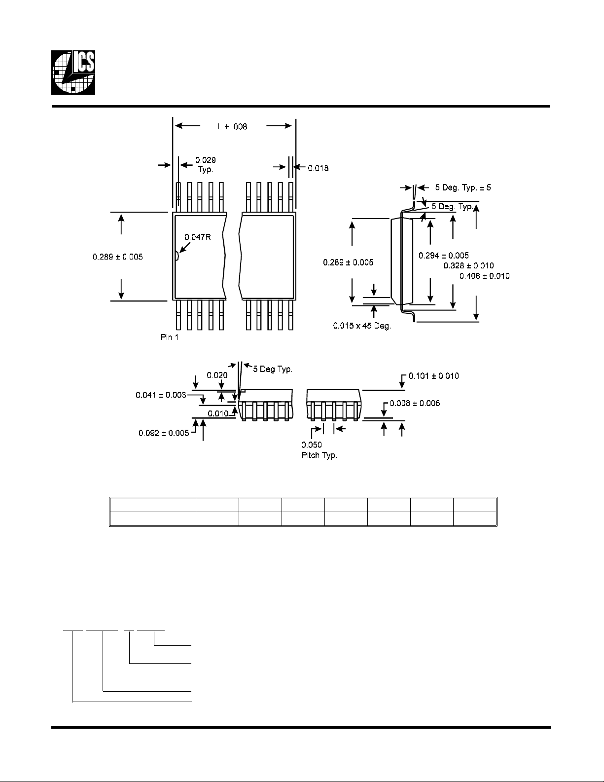
LEAD COUNT 14L 16L 18L 20L 24L 28L 32L
DIMENSION L 0.354 0.404 0.454 0.504 0.604 0.704 0.804
Ordering Information
ICS1572M-101 or ICS1572M-301
Example:
ICS XXXX M -XXX
Pattern Numbe r (2 or 3 digit numbe r for par ts with RO M code patterns )
Package Type
M=SOIC
Device Type (consists of 3 or 4 digit numbe rs )
Prefix
ICS, AV=Standard Device; GSP=Genloc k Device
SOIC Packages (wide body)
19
 Loading...