Integrated
Circuit
Systems, Inc.
General Description Features
ICS2509C
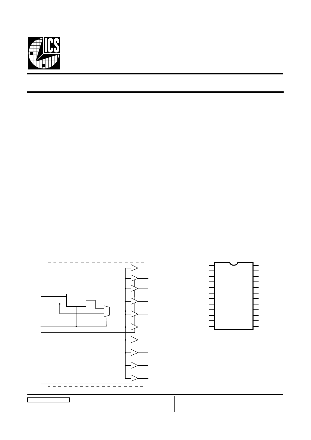
Block Diagram
3.3V Phase-Lock Loop Clock Driver
2509 C Rev C 06/15/01
Pin Configuration
24 Pin TSSOP
4.40 mm. Body, 0.65 mm. pitch
The ICS2509C is a high performance, low skew, low jitter
clock driver. It uses a phase lock loop (PLL) technology to
align, in both phase and frequency, the CLKIN signal with
the CLKOUT signal. It is specifically designed for use with
synchronous SDRAMs. The ICS2509C operates at 3.3V VCC
and drives up to nine clock loads.
One bank of five outputs and one bank of four outputs provide
nine low-skew, low-jitter copies of CLKIN. Output signal
duty cycles are adjusted to 50 percent, independent of the
duty cycle at CLKIN. Each bank of outputs can be enabled or
disabled separately via control (OEA and OEB) inputs. When
the OE inputs are high, the outputs align in phase and
frequency with CLKIN; when the OE inputs are low, the
outputs are disabled to the logic low state.
The ICS2509C does not require external RC filter
components. The loop filter for the PLL is included on-chip,
minimizing component count, board space, and cost. The
buffer mode shuts off the PLL and connects the input directly
to the output buffer. This buffer mode, the ICS2509C can be
use as low skew fanout clock buffer device. The ICS2509C
comes in 24 pin 173mil Thin Shrink Small-Outline package
(TSSOP) package.
• Meets or exceeds PC133 registered DIMM
specification 1.1
• Spread Spectrum Clock Compatible
• Distributes one clock input to one bank of five and one
bank of four outputs
• Separate output enable(OEA,OEB) for each output bank
• Operating frequency 25 MHz to 175 Mhz
• External feedback input (FBIN) terminal is used to
synchrionize the outputs to the clock input
• No external RC network required
• Operates at 3.3V Vcc
• Plastic 24-pin 173mil TSSOP package
FBIN
CLKIN
AVC C
OEA
OEB
PLL
CLKA0
FBOUT
CLKA1
CLKA2
CLKA3
CLKA4
CLKB0
CLKB1
CLKB2
CLKB3
AGND
VCC
CLKA0
CLKA1
CLKA2
GND
GND
CLKA3
CLKA4
VCC
OEA
FBOUT
CLKIN
VCC
CLKB0
CLKB1
GND
GND
CLKB2
CLKB3
VCC
OEB
FBIN
AVCC
ICS2509C
1
2
3
4
5
6
7
8
9
10
11
12
24
23
22
21
20
19
18
17
16
15
14
13
ICS reserves the right to make changes in the device data identified in
this publication without further notice. ICS advises its customers to
obtain the latest version of all device data to verify that any
information being relied upon by the customer is current and accurate.

2
ICS2509C
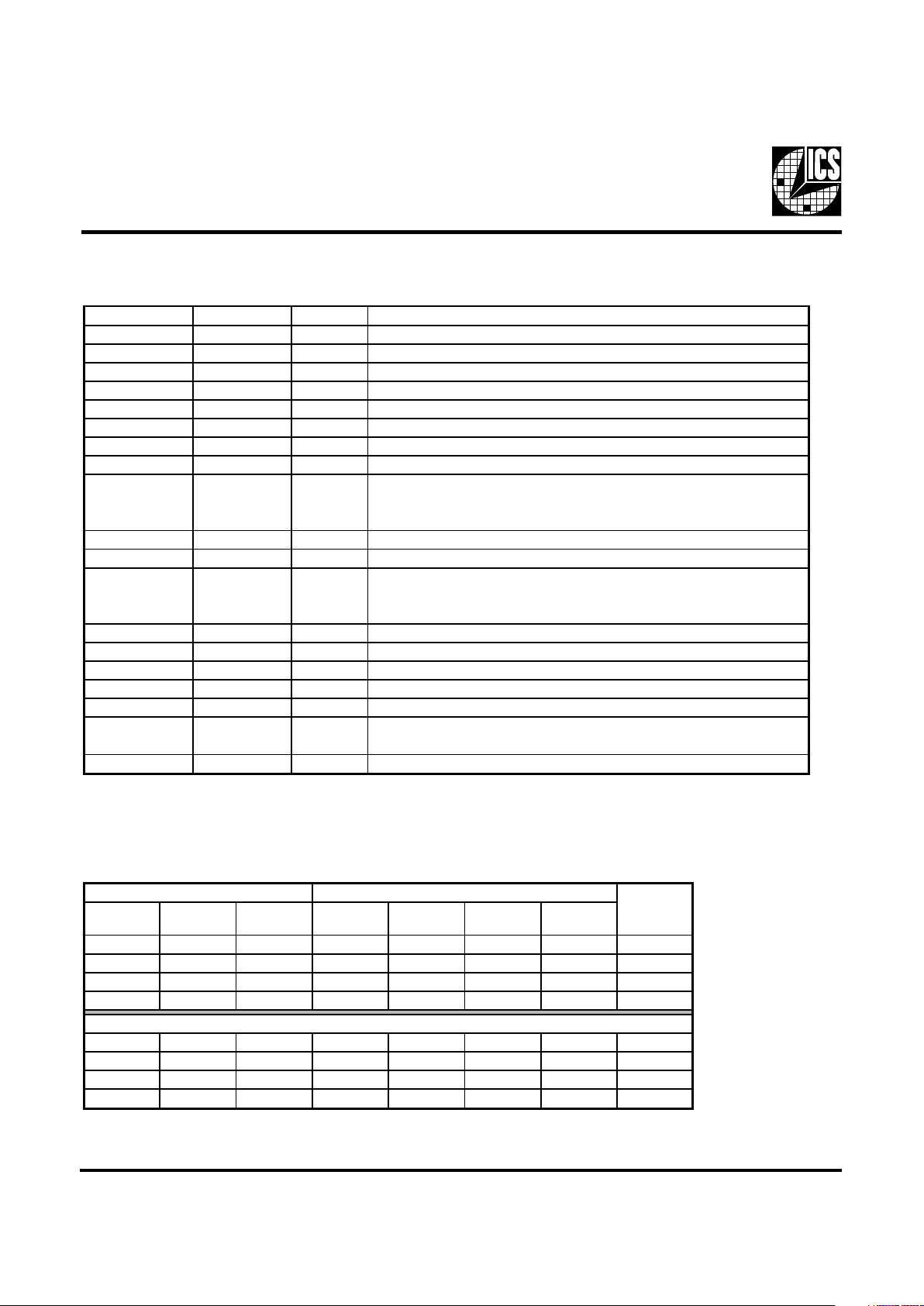
Pin Descriptions
Note:
1. Weak pull-ups on these inputs
PIN NUMBER PIN NAME TYPE DESCRIPTION
1 AGND PWR Analog Ground
2, 10, 15 VCC PWR Power Supply (3.3V)
3 CLKA0 OUT Buffered clock output, Bank A
4 CLKA1 OUT Buffered clock output, Bank A
5 CLKA2 OUT Buffered clock output, Bank A
6, 7, 18, 19 GND PWR Ground
8 CLKA3 OUT Buffered clock output, Bank A
9 CLKA4 OUT Buffered clock output, Bank A
11
OEA
1
IN
Output enable (has internal pull_up). When high, normal operation.
When low bank A clock outputs are disabled to a logic low state.
12 FBOUT OUT Feedback output
13 FBIN IN Feedback input
14
OEB
1
IN
Output enable (has internal pull_up). When high, normal operation.
When low bank B clock outputs are disabled to a logic low state.
16 CLKB3 OUT Buffered clock output. Bank B
17 CLKB2 OUT Buffered clock output. Bank B
20 CLKB1 OUT Buffered clock output. Bank B
21 CLKB0 OUT Buffered clock output. Bank B
22 VCC PWR Power Supply (3.3V) digital supply.
23 AVCC IN
Analog power supply (3.3V). When input is ground PLL is off and
bypassed.
24 CLKIN IN Clock input
Functionality
OEA OEB AVCC
CLKA
(0:4 )
CLKB
(0:3)
FBOUT Source
0 0 3.33 0 0 Driven PLL N
0 1 3.33 0 Driven Driven PLL N
1 0 3.33 Driven 0 Driven PLL N
1 1 3.33 Driven Driven Driven PLL N
00000DrivenCLKINY
0100DrivenDrivenCLKINY
1 0 0 Driv en 0 Driven CLKIN Y
110
Driven Driven
Driven CLKIN Y
Test mode:
When AVCC is 0, shuts off the PLL and connects the input directly to the output buffers
Buffer Mode
INPUTS OUTPUTS
PLL
Shutdown

3
ICS2509C
Absolute Maximum Ratings
Supply Voltage (AVCC) . . . . . . . . . . . . . . . . . . . AVCC < (Vcc + 0.7V)
Supply Voltage (VCC) . . . . . . . . . . . . . . . . . . . . 4.3 V
Logic Inputs . . . . . . . . . . . . . . . . . . . . . . . . . . . . GND –0.5 V to Vcc +0.5 V
Ambient Operating Temperature . . . . . . . . . . . . 0°C to +70°C
Storage Temperature . . . . . . . . . . . . . . . . . . . . . . –65°C to +150°C
Stresses above those listed under Absolute Maximum Ratings may cause permanent damage to the device. These ratings are
stress specifications only and functional operation of the device at these or any other conditions above those listed in the
operational sections of the specifications is not implied. Exposure to absolute maximum rating conditions for extended
periods may affect product reliability.
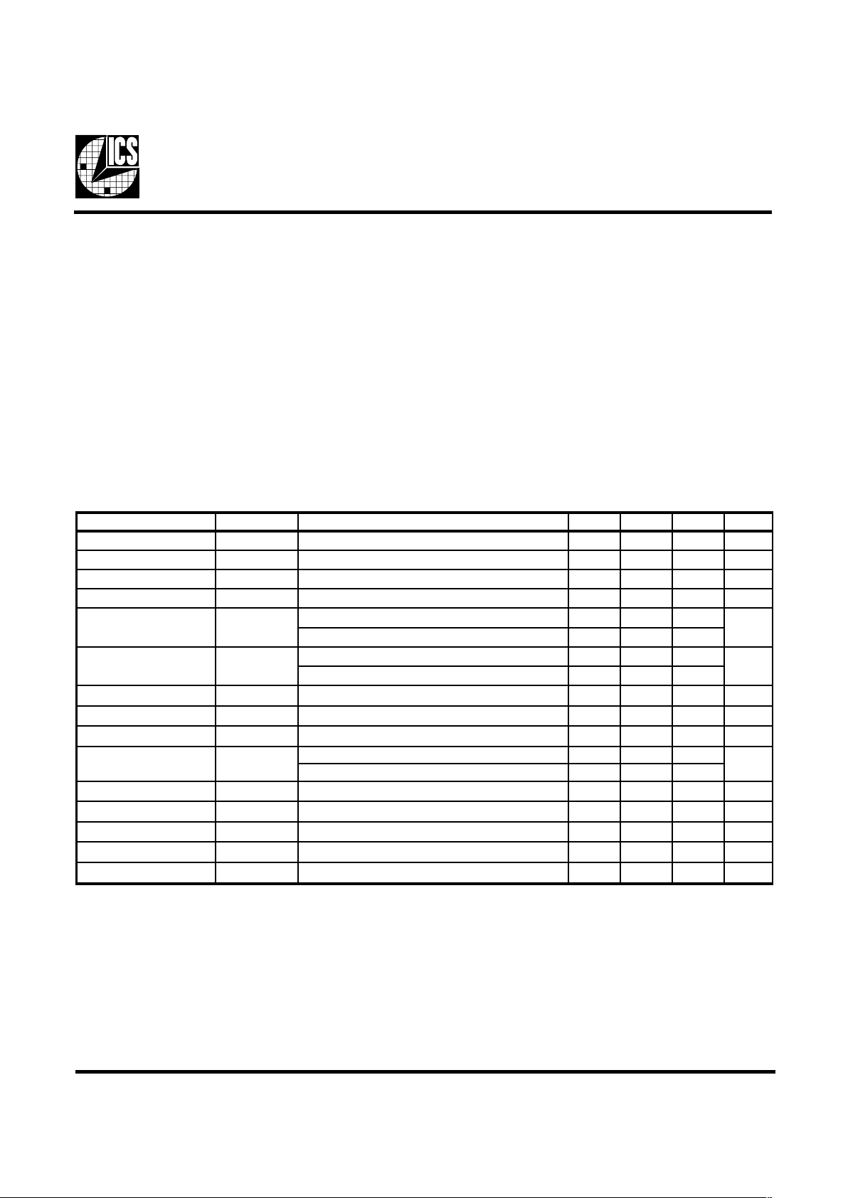
Electrical Characteristics - OUTPUT
TA = 0 - 70C; VDD = V
DDL
= 3.3 V +/-
10%; C
L
= 20 - 30 pF; RL = 470 Ohms (unless otherwise state
d)
PARAMETER
S
YMBOL
CO
NDITION
S
MIN TYP MAXUNIT
S
Output Impedance R
DSP
VO = VDD*(0.5) 36
Ω
Output Impedance R
DSN
VO = VDD*(0.5) 32
Ω
Output High Voltage V
OH
IOH = -8 mA 2.4 2.9 V
Output Low Voltage V
OL
IOL = 8 mA 0.25 0.4 V
V
OH
= 2.4 V -26 -13.6
V
OH
= 2.0 V -37 -22
V
OL
= 0.8 V 19 25
V
OL
= 0.55 V 13 17
Rise Time
1
T
r
VOL = 0.8 V, VOH = 2.0 V 0.5 1.4 2.1 ns
Fall Time
1
T
f
VOH = 2.0 V, VOL = 0.8 V 0.5 1.5 2.7 ns
Duty Cycle
1
D
t
VT = 1.5 V;CL=30 pF 45 50 55 %
at 66-100 MHz ; loaded outputs 52 100
at 133 MHz ; loaded outputs 39 75
Absolute Jitter
1
Tjabs 10000 cycles; CL = 30 pF 57 ps
Skew
1
T
sk
VT = 1.5 V (Window) Output to Output 80 150 ps
Phase error
1
T
pe
VT = Vdd/2; CLKIN-FBIN -150 40 150 ps
Phase error Jitter
1
T
pe
3
VT = Vdd/2; CLKIN-FBIN; Delay Jitter -50 35 50 ps
Del
ay Input-Output
1
D
R1
VT = 1.5 V; PLL_EN = 0
3.3 3.7 ns
1
Guaranteed by design, not 100% tested in production.
Cycle to Cycle jitter
1
Tcyc-cyc ps
Output High Current
Output Low Current
I
OH
I
OL
mA
mA
 Loading...