

Integrated
Circuit
Systems, Inc.
Description Features
ICS1574B
Block Diagram
User Programmable Laser Engine Pixel Clock Generator
1574B 8/31/00
•
Supports high resolution laser graphics. PLL/VCO
frequency re-programmable through serial interface
port to 400 MHz; allows less than ±1.5ns pixel clock
resolution.
•
Laser pixel clock output is synchronized with
conditioned beam detect input
•
Ideal for laser printer, copier and FAX pixel clock
applications
•
On-chip PLL with internal loop filter
•
On-chip XTAL oscillator frequency reference
•
Resettable, programmable counter gives glitch-free
clock alignment
•
Single 5 volt power supply
•
Low power CMOS technology
•
Compact – 16-pin 0.150" skinny SOIC package
•
User re-programmable clock frequency supports
zoom and gray scale functions
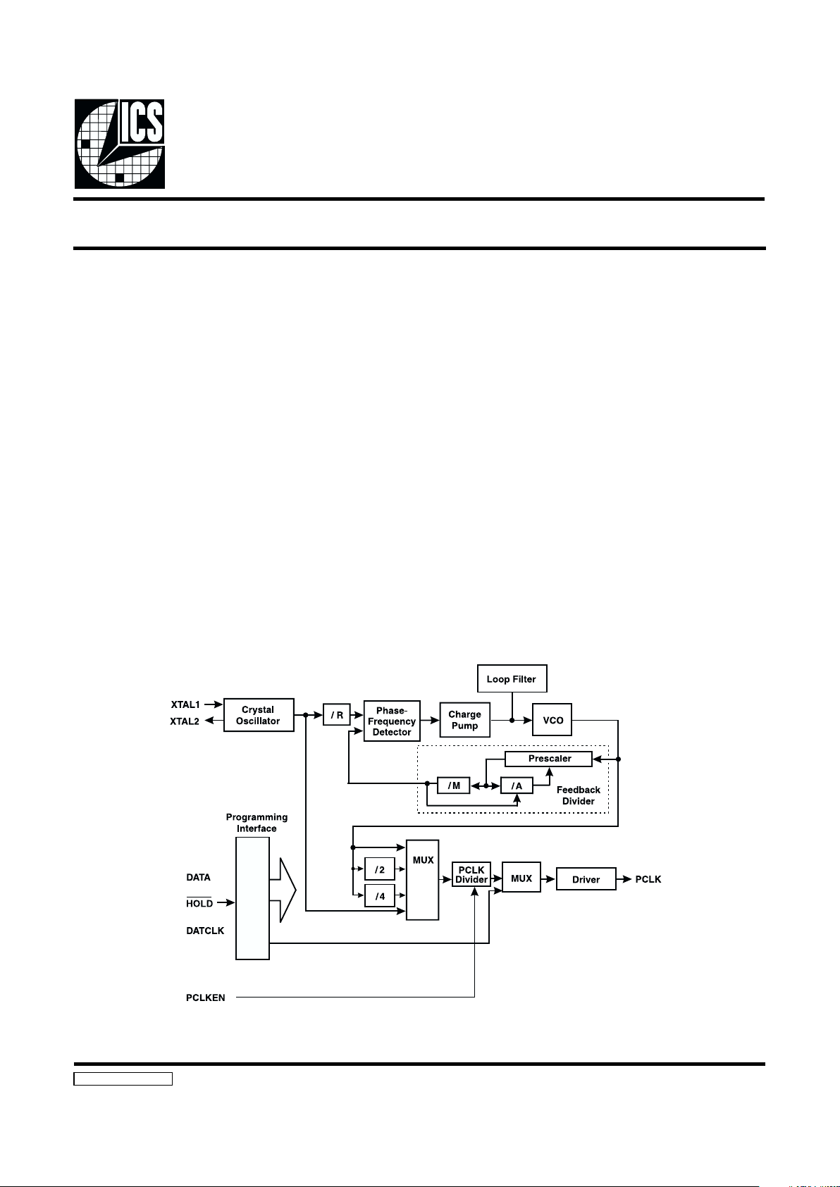
The ICS1574B is a very high performance monolithic phaselocked loop (PLL) frequency synthesizer designed for laser
engine applications. Utilizing ICS’s advanced CMOS mixedmode technology, the ICS1574B provides a low cost solution
for high-end pixel clock generation for a variety of laser engine product applications.
The pixel clock output (PCLK) frequency is derived from the
main clock by a programmable resettable divider.
Operating frequencies are fully programmable with direct
control provided for reference divider, feedback divider and
post-scaler.
Figure 1
ICS1574B
2
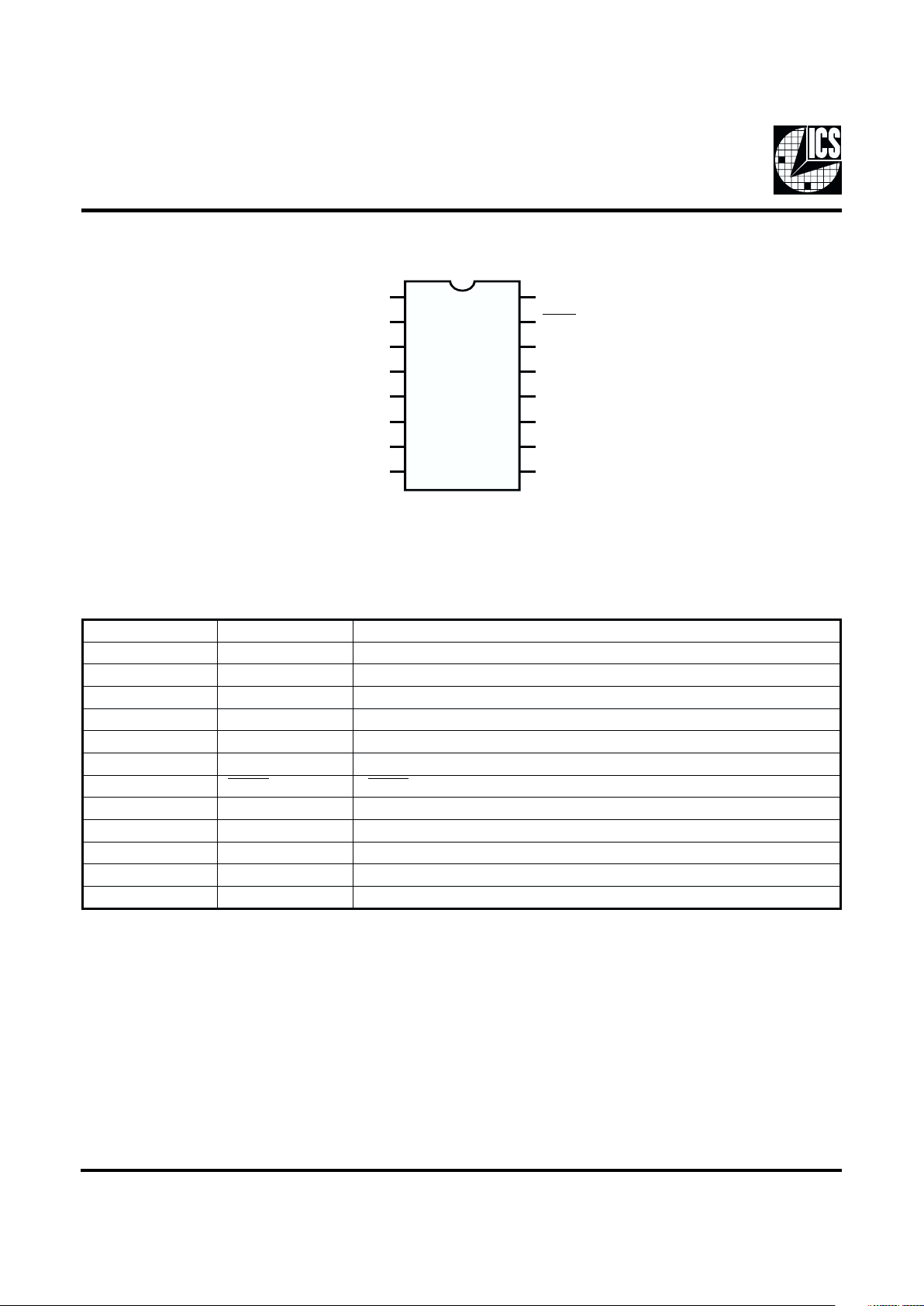
Pin Configuration
16-Pin Skinny SOIC
Pin Descriptions
REBMUNNIPEMANNIPNOITPIRCSED
7KLCP.tuptuokcolclexiP
1NEKLCP.)tupnI(elbanEKLCP
21LATX .tupniycneuqerfecnereferlanretxe/1noitcennoclatsyrcztrauQ
32LATX.2noitcennoclatsyrcztrauQ
4KLCTAD.)tupnI(kcolCataD
61ATAD.)tupnI(ataDretsigeRlaireS
51DLOH.)tupnI(DLOH
41tseT).SSVotdetcennocebtsuM(.tseT
11,01,9,8devreseR).tcennoCtoNoD(.devreseR
31DDV.)margaidnoitacilppaeeS.V5+(rewopmetsysLLP
21ODDV.)V5+(rewopegatstuptuO
6,5SSV).detcennocebtsumsniphtoB(.dnuorgeciveD
PCLKEN
XTAL1
XTAL2
DATCLK
VSS
VSS
PCLK
Reserved
(Do Not Connect)
DATA
HOLD
TEST
VDD
VDDO
Reserved
(Connect to VSS))
(Do Not Connect)
(Do Not Connect)
(Do Not Connect)
Reserved
Reserved
1
2
3
4
5
6
7
8
16
15
14
13
12
11
10
9
ICS1574B
3
ICS1574B
PCLK Programmable Divider
The ICS1574B has a programmable divider (referred to in Fig-
ure 1 as the PCLK divider) that is used to generate the PCLK
clock frequency for the pixel clock output. The modulus of
this divider may be set to 3, 4, 5, 6, 8, 10, 12, 16 or 20 under
register control. The design of this divider permits the output
duty factor to be 50/50, even when an odd modulus is selected. The input frequency to this divider is the output of the
PLL post-scaler described below:
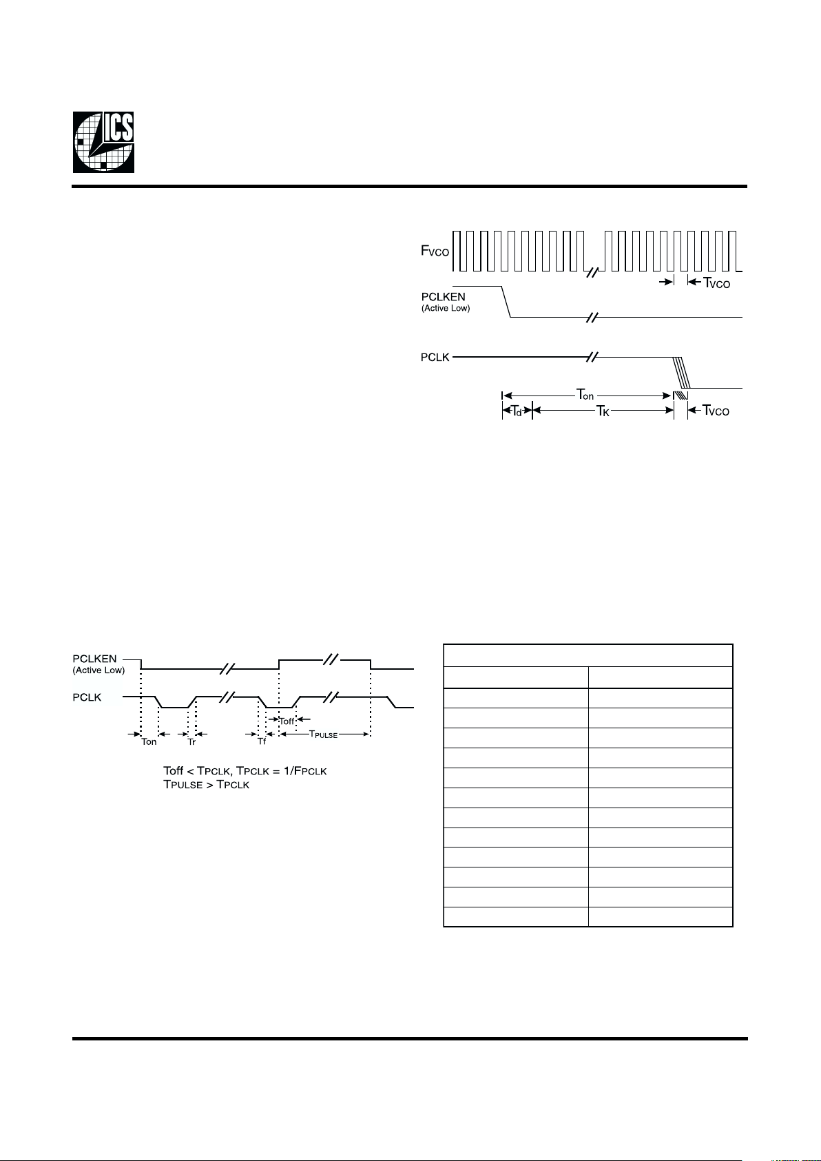
The phase of the PCLK output is aligned with the internal
high frequency PLL clock (F
VCO
) immediately after the assertion of the PCLKEN input pulse (active low if PCLKEN_POL
bit is 0 or active high if PCLKEN_POL bit is 1).
When PCLKEN is deasserted, the PCLK output will complete
its current cycle and remain at VDD until the next PCLKEN
pulse. The minimum time PCLKEN must be disabled
(T
PULSE
) is 1/F
PCLK
.
See Figure 2a for an example of PCLKEN enable (negative
polarity) vs. PCLK timing sequences.
Figure 2a
Figure 2b
seulaVK
rediviDKLCPK
32
a45.3
b43
55.4
65.3
a85.5
b85
017
215.6
a615.9
b619
0221
TK = K •T
VCO
Td = LOGIC PROP.DELAY TIME
(typically 9ns with a 10pF load on PCLK)
T
VCO
= 1/F
VCO
The resolution of Ton is one VCO cycle.
The time required for a PCLK cycle start following a PCLKEN
enable is described by Figure 2b and the following table:
Typical values for Tr and Tf with a 10pF load on PCLK are
1ns.
ICS1574B
4
PLL Post-Scaler
A programmable post-scaler may be inserted between the
VCO and the PCLK divider of the ICS1574B. This is useful in
generating lower frequencies, as the VCO has been optimized
for high-frequency operation. The post-scaler is not affected
by the PCLKEN input.
The post-scaler allows the selection of:
• VCO frequency
• VCO frequency divided by 2
• VCO frequency divided by 4
• AUX-EN Test Mode
PLL Synthesizer Description —
Ratiometric Mode
The ICS1574B generates its output frequencies using phaselocked loop techniques. The phase-locked loop (or PLL) is a
closed-loop feedback system that drives the output frequency
to be ratiometrically related to the reference frequency provided to the PLL (see Figure 1). The reference frequency is
generated by an on-chip crystal oscillator or the reference frequency may be applied to the ICS1574B from an external
frequency source.
The phase-frequency detector shown in the block diagram
drives the voltage-controlled oscillator, or VCO, to a frequency that will cause the two inputs to the phase-frequency
detector to be matched in frequency and phase. This occurs
when:
back divider makes use of a dual-modulus prescaler technique that allows the programmable counters to operate at
low speed without sacrificing resolution. This is an improvement over conventional fixed prescaler architectures that
typically impose a factor-of-four (or larger) penalty in this respect.
Table 1 permits the derivation of “A” & “M” converter pro-
gramming directly from desired modulus.
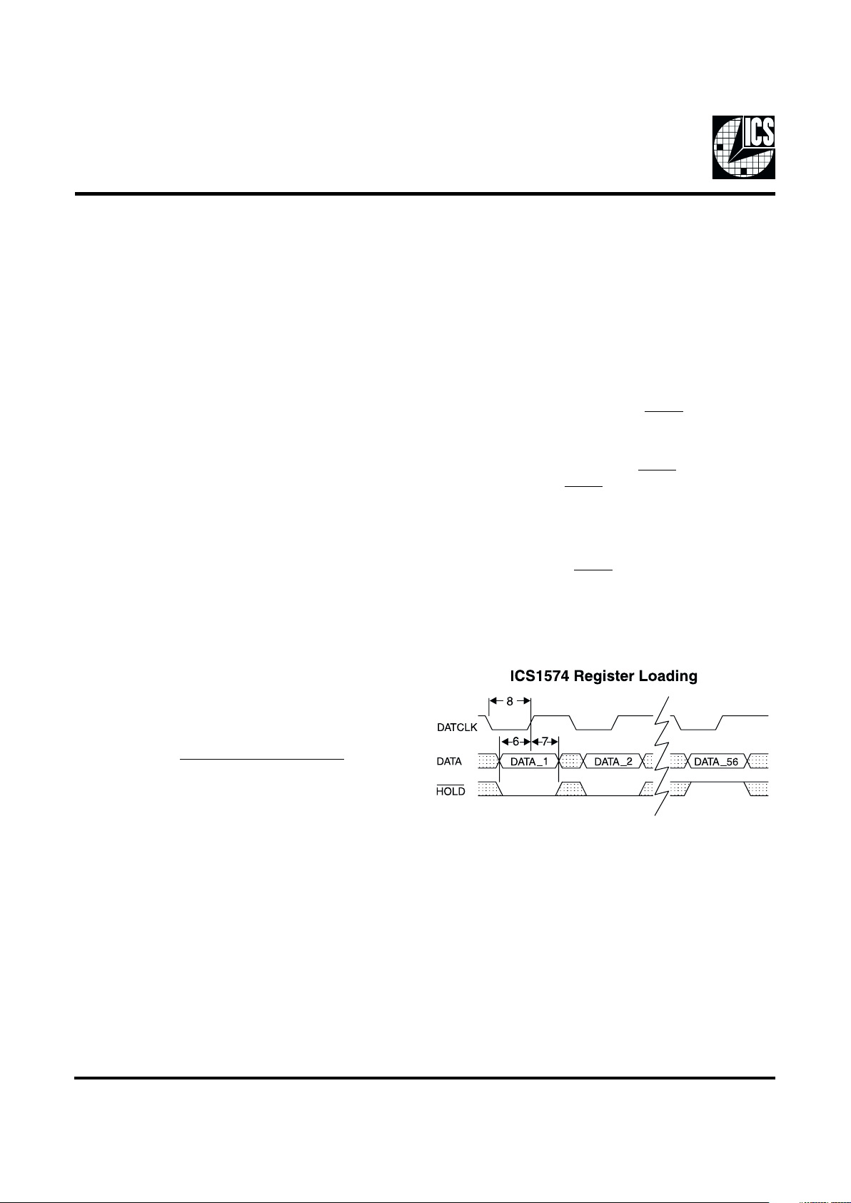
Digital Inputs
The programming of the ICS1574B is performed serially
by using the DATCLK, DATA, and HOLD pins to load an
internal shift register.
DATA is shifted into the register on the rising edge of
DATCLK. The logic value on the HOLD pin is latched at
the same time. When HOLD is low, the shift register may
be loaded without disturbing the operation of the
ICS1574B. When high, the shift register outputs are transferred to the control registers, and the new programming
information becomes active. Ordinarily, a high level
should be placed on the HOLD pin when the last data bit is
presented. See Figure 3 for the programming sequence.
The PCLKEN input polarity may be programmed under
register control via Bit 39.
F
(VCO)
: =
F(XTAL1)
• Feedback Divider
Reference Divider
Figure 3
This expression is exact; that is, the accuracy of the output
frequency depends solely on the reference frequency provided to the part (assuming correctly programmed dividers).
The VCO gain is programmable, permitting the ICS1574B to
be optimized for best performance at all operating frequencies.
The reference divider may be programmed for any modulus
from 1 to 128 in steps of one.
The feedback divider may be programmed for any modulus
from 37 through 392 in steps of one. Any even modulus from
392 through 784 can also be achieved by setting the “double”
bit which doubles the feedback divider modulus. The feed-
Output Description
The PCLK output is a high-current CMOS type drive
whose frequency is controlled by a programmable divider
that may be selected for a modulus of 3, 4, 5, 6, 8, 10, 12,
16 or 20. It may also be suppressed under register control
via Bit 46.

5
ICS1574B
NIAGOCVYCNEUQERFXAM
4zHM001
5zHM002
6zHM003
7zHM004
Reference Oscillator
and Crystal Selection
The ICS1574B has circuitry on-board to implement a
Pierce oscillator with the addition of only one external
component, a quartz crystal. Pierce oscillators operate the
crystal in
anti- (also called parallel-) resonant mode. See the AC
Characteristics for the effective capacitive loading to
specify when ordering crystals.
Series-resonant crystals may also be used with the
ICS1574B. Be aware that the oscillation frequency will be
slightly higher than the frequency that is stamped on the
can (typically 0.025 – 0.05%).
As the entire operation of the phase-locked loop depends
on having a stable reference frequency, we recommend
that the crystal be mounted as closely as possible to the
package. Avoid routing digital signals or the ICS1574B
outputs underneath or near these traces. It is also desirable
to ground the crystal can to the ground plane, if possible.
If an external reference frequency source is to be used with
the ICS1574B, it is important that it be jitter-free. The rising and falling edges of that signal should be fast and free
of noise for best results.
The loop phase can be locked to either the rising or falling
edges of the XTAL1 input signals, and is controlled by
Bit 56.
Power-On Initialization
The ICS1574B has an internal power-on reset circuit that
performs the following functions:
1) Selects the modulus of the PCLK divider to
be four (4).
2) Sets the multiplexer to pass the reference
frequency to PCLK divider input.
These functions should allow initialization for most applications that cannot immediately provide for register
programming upon system power-up.
Because the power-on reset circuit is on the VDD supply,
and because that supply is filtered, care must be taken to
allow the reset to de-assert before programming. A safe
guideline is to allow 20 microseconds after the VDD supply reaches 4 volts.
Programming Notes
• VCO Frequency Range: Use the post-divider to keep the
VCO frequency as high as possible within its operating
range.
• Divider Range: For best results in normal situations
keep the reference divider modulus as short as possible
(for a frequency at the output of the reference divider in
the few hundred kHz to several MHz range). If you
need to go to a lower phase comparator reference frequency (usually required for increased frequency
accuracy), that is acceptable, but jitter performance will
suffer somewhat.
• VCO Gain Programming: Use the minimum gain which
can reliably achieve the VCO frequency desired, as
shown here:
• Phase Detector Gain: For most applications and divider
ranges, set P [1, 0] = 10 and set P[2] = 1. Under some
circumstances, setting the P [2] bit “on” can reduce
jitter. During operation at exact multiples of the crystal
frequency, P[2] bit = 0 may provide the best jitter performance.
Board Test Support
It is often desirable to statically control the levels of the
output pins for circuit board test. The ICS1574B supports
this through a register programmable mode, AUX-EN.
When this mode is set, a register bit directly controls the
logic level of the PCLK pin. This mode is activated when
the S[0] and S[1] bits are both set to logic 1. See Register
Mapping for details.
ICS1574B
6
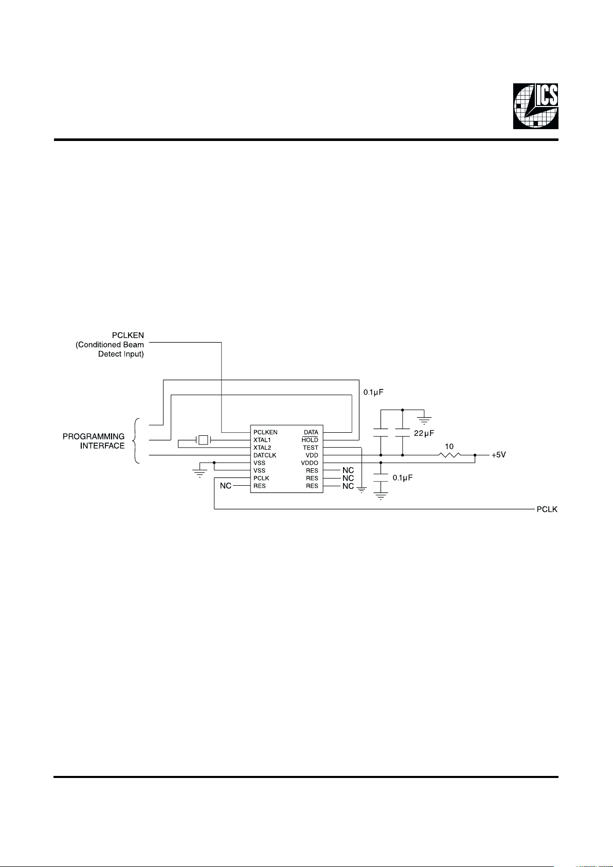
Figure 4
Power Supplies and Decoupling
The ICS1574B has two VSS pins to reduce the effects of
package inductance. Both pins are connected to the same
potential on the die (the ground bus). BOTH of these pins
should connect to the ground plane of the PCB as close to
the package as is possible.
The ICS1574B has a VDDO pin which is the supply of +5
volt power to the output driver. This pin should be connected to the power plane (or bus) using standard
high-frequency decoupling practice. That is, capacitors
should have low series inductance and be mounted close to
the ICS1574B.
The VDD pin is the power supply pin for the PLL synthesizer circuitry and other lower current digital functions.
We recommend that RC decoupling or zener regulation be
provided for this pin (as shown in the recommended application circuitry). This will allow the PLL to “track”
through power supply fluctuations without visible effects.
See Figure 4 for typical external circuitry.

7
ICS1574B
]3[KLCP]2[KLCP]1[KLCP]0[KLCPSULUDOM
0000 3
0001 )a(4
0010 )b(4
0011 5
0100 6
0101 )a(8
0110 )b(8
0111 01
1X0 0 21
1X0 1 )a(61
1X 1 0 )b(61
1X 1 1 02
]1[S]0[SNOITPIRCSED
00
KLCPehtfotuptuoehT.)LLP(F=)KLC(F.1=relacs-tsoP
.tuptuoKLCPehtsevirdredivid
01
ehtfotuptuoehT.2/)LLP(F=)KLC(F.2=relacs-tsoP
.tuptuoKLCPehtsevirdredividKLCP
10
ehtfotuptuoehT.4/)LLP(F=)KLC(F.4=relacs-tsoP
.tuptuoKLCPehtsevirdredividKLCP
11
LCP_XUAehT.EDOMTSETNE-XUA
K
ehtsevirdtib
.tuptuoKLCP
Register Mapping — ICS1574B
NOTE: It is not necessary to understand the function of these bits to use the ICS1574B. PC Software is available from ICS to
automatically generate all register values based on requirements. Contact factory for details.
BIT(S) BIT REF. DESCRIPTION
1 – 4 PCLK[0]..PCLK[3] Sets PCLK divider modulus according to this table.
These bits are set to implement a divide-by-four on power-up.
(X = Don't Care)
5, 6 Reserved Must be set to 0.
7 Reserved Must be set to 1.
8 SELXTAL Normally set to 0. When set to logic 1, passes the reference
frequency to the post-scaler instead of the PLL output
(defaults to 1 on power-up).
9 Reserved Must be set to 0.
10 Reserved Must be set to 1.
11, 12 Reserved Must be set to 0.
13 – 14 S[0]..S[1] PLL post-scaler / test mode select bits.

ICS1574B
8
]1[P]0[PNIAG
)naidar/Aµ(
00 50.0
01 51.0
10 5.0
11 5.1
]2[V]1[V]0[V
NIAGOCV
)tloV/zHM(
100 03
10 1 54
110 06
111 08
BIT(S) BIT REF. DESCRIPTION
15 Reserved Must be set to 0.
16 AUX_PCLK Must be set to 0 except when in the AUX-EN test mode.
When in the AUX-EN test mode, this bit controls the
PCLK output.
17 – 24 Reserved Must be set to 0.
25 – 27 V[0]..V[2] Sets the gain of VCO
28 Reserved Must be set to 1.
29 – 30 P[0]..P[1] Sets the gain of the phase detector according to this table:
31 Reserved Must be set to 0.
32 P[2] Phase detector tuning bit. Should normally be set to one.
See text.
33 – 38 M[0]..M[5] M counter control bits. Modulus = value + 1.
39 PCLKEN_POL When = 0, PCLK output enabled when PCLKEN input is
low. When = 1, PCLK output enabled when PCLKEN input
is high.
40 DBLFREQ Doubles modulus of dual-modulus prescaler (from 6 / 7 to
12/14).
41 – 44 A[0]..A[3] Controls A counter. When set to zero, modulus = 7.
Otherwise, modulus = 7 for "value" underflows of the
prescaler, and modulus = 6 thereafter until M counter
underflows.

9
ICS1574B
BIT(S) BIT REF. DESCRIPTION
45 Reserved Must be set to 1.
46 PCLK_EN Must be set to 0.
Disables the PCLK divider when set to 1 regardless of
PCLKEN input state.
47, 48 Reserved Must be set to 0.
49 – 55 R[0]..R[6] Reference divider modulus control bits.
Modulus = value +1.
56 REF_POL PLL locks to rising edge of XTAL1 input when
REFPOL = 1, falling edge of XTAL1 when REFPOL = 0.

ICS1574B
10
Table 1 — "A" & "M" Divider Programming
Feedback Divider Modulus Table
Notes: To use this table, find the desired modulus in the table. Follow the column up to find the A divider programming values. Follow the
row to the left to find the M divider programming. Some feedback divisors can be achieved with two or three combinations of divider settings.
Any are acceptable for use.
The formula for the effective feedback modulus is: N =[(M +1) • 6] +A
except when A=0, then: N=(M +1) • 7
Under all circumstances: A ≤ M
-]0[A..]2[A100010110001101011111000-]0[A..]2[A100010110001101011111000
]0[M..]5[M]0[M..]5[M
0000007000001991002102202302402502132
1000003141100001502602702802902012112832
010000910212010001112212312412512612712542
11000052627282110001712812912022122222322252
0010001323334353001001322422522622722822922952
101000738393041424101001922032132232332432532662
01100034445464748494011001532632732832932042142372
1110009405152535455565111001142242342442542642742082
0001005565758595061636000101742842942052152252352782
1001001626364656667607100101352452552652752852952492
0101007686960717273777010101952062162262362462562103
1101003747576777879748110101562662762862962072172803
0011009708182838485819001101172272372472572672772513
1011005868788898091989101101772872972082182282382223
01110019293949596979501011101382482582682782882982923
111100798999001101201301211111101982092192292392492592633
000010301401501601701801901911000011592692792892992003103343
100010901011111211311411511621100011103203303403503603703053
010010511611711811911021121331010011703803903013113213313753
110010121221321421521621721041110011313413513613713813913463
001010721821921031131231331741001011913023123223323423523173
101010331431531631731831931451101011523623723823923033133873
011010931041141241341441541161011011133233333433533633733583
111010541641741841941051151861111011733833933043143243343293
000110151251351451551651751571000111343443543643743843943993
100110751851951061161261361281100111943053153253353453553604
010110361461561661761861961981010111553653753853953063163314
110110961071171271371471571691110111163263363463563663763024
001110571671771871971081181302001111763863963073173273373724
101110181281381481581681781012101111373473573673773873973434
011110781881981091191291391712011111973083183283383483583144
111110391491591691791891991422111111583683783883983093193844

11
ICS1574B
Absolute Maximum Ratings
VDD, VDDO (measured to VSS) . . . . . . . . 7.0 V
Digital Inputs . . . . . . . . . . . . . . . . . . . . . . . V
SS
– 0.5 V to VDD +0.5 V
Digital Outputs . . . . . . . . . . . . . . . . . . . . . . V
SS
– 0.5 V to V
DDO
+0.5 V
Ambient Operating Temperature . . . . . . . – 55°C to +125° C
Storage Temperature . . . . . . . . . . . . . . . . . – 65° C to +15 0 °C
Junction Temperature . . . . . . . . . . . . . . . . . 175°C
Soldering Temperature . . . . . . . . . . . . . . . . 260° C
DC Electrical Characteristics
TTL-Compatible Inputs (DATCLK, DATA, HOLD, PCLKEN)
Recommended Operating Conditions
VDD, VDDO (measured to VSS) . . . . . . . . 4.75 to 5.25 V
Operating Temperature (Ambient) . . . . . . 0 to +70°C
RETEMARAPLOBMYSSNOITIDNOCNIMXAMSTINU
egatloVhgiHtupnIV
HI
0.2VDD5.0+V
egatloVwoLtupnIV
LI
V
SS
5.0– 8.0V
tnerruChgiHtupnII
HI
V
HI
DDV= — 01Aµ
tnerruCwoLtupnII
LI
V
LI
0.0= — 002Aµ
ecnaticapaCtupnIC
NI
— 8Fp
)tupniKLCTAD(sisiretsyHV
SYH
V5=DDV02.06.V
tupnI1LATX
)ycneuqerFecnerefeRlanretxE(
RETEMARAPLOBMYSSNOITIDNOCNIMXAMSTINU
egatloVhgiHtupnIV
HX
57.3VDD5.0+V
egatloVwoLtupnIV
LX
V
SS
5.0– 52.1V
KLCP
RETEMARAPLOBMYSSNOITIDNOCNIMXAMSTINU
I(egatloVhgiHtuptuO
HO
)Am0.4=4.2 — V
I(egatloVwoLtuptuO
LO
)Am0.8= — 4.0V

ICS1574B
12
Ordering Information
ICS1574BM / ICS1574BEB
16-Pin Skinny SOIC Package
AC Electrical Characteristics
ICS 1574B M
Package Type
M = SOIC • EB = Evaluation Board
Device Type
Prefix
ICS, AV = Standard Device • GSP = Genlock Device
Example:
RETEMARAPLOBMYSNIMPYTXAMSTINU
ycneuqerFOCVF
OCV
04004zHM
ycneuqerFlatsyrCF
LATX
502zHM
ecnaticapaCgnidaoLrotallicsOlatsyrCC
RAP
02Fp
)yllanretxenevirdnehw(emiThgiH1LATXT
IHX
8sn
)yllanretxenevirdnehw(emiTwoL1LATXT
OLX
8sn
)%1nihtiwot(emiTeriuqcALLPT
KCOL
005sµ
tnerruCylppuSDDVI
DD
51.d.b.tAm
tnerruCylppuSODDVI
ODD
02.d.b.tAm
stupnIlatigiD
emiTputeS~DLOH/ATAD01sn
emiTdloH~DLOH/ATAD01sn
T(htdiWesluPKLCTAD
ih
Trool)02sn
latigiD
tuptuO
etartuptuoKLCPPF
KCOLC
031zHM
 Loading...