

Page 1
Integrated
Circuit
Systems , In c.
ICS1567
Differential Output Video Dot Clock Generator
General Description
The ICS1567 is a very high performance monolithic PLL
frequency synthesizer. Utilizing ICS’s advanced CMOS
mixed-mode technology, the ICS1567 provides a low cost
solution for high-end video clock generation, and for telecom
system clock generation.
The ICS1567 has di ffer enti al vi deo cloc k ou tpu ts (C LK and
CLK) that are compatible with industry standar d video DACs
& RAMDACs. An additional clock output,
LD, is provided,
whose frequency is divided down from the main clock by a
prog rammable divider.
Operating frequencies are selectable from a pre-programmed
(customer -defined) table. An on-c hip crystal oscillator for generati ng th e re fe rence fre que ncy is provi de d on the ICS1567.
Programming of the ICS1567 is acc om pl is he d vi a f re quen cy
select pins on the package. The ICS1567 has five lines plus a
STROBE pin which permits selection of 32 fr equencie s. Reset
of the pipel ine delay on Brooktree RAMDACs is auto matically
performed on a rising edge of the STROBE line.
Features
•• High frequency operation for extended video modes - up
to 180 MHz
•• Compatible wit h Brooktr ee high perform anc e RAMDAC s
a) Differenti al output clocks wi th ECL logic leve ls
b) Programmable divider modulus fo r loa d clock
c) Circuitry included for automatic reset of Brooktree
RAMDAC pipeline delay
•• Low cost - el imina tes ne ed fo r mul tiple ECL c ryst al cloc k
oscillators in video disp lay syste ms
•• Strobe d/ Tr ansparent frequency selec t op ti on s
•• 32-user selected mask-programmable frequencies
•• Fast acquisition of selected frequencies, strobed or non-
strobed
•• Advanced PL L for low ph ase -j itte r
•• Dynamic c ont rol of VC O se nsi ti vit y p rovi di ng o ptimized
loop gai n ove r entire freque ncy range
•• Small footprin t - 16-pin wide body (300 mil) SOIC
FS0 1 16 FS1
XT AL1 2 15 FS2
XT AL2 3 14 FS3
STROBE 4 13 VDD
VSS 5 12 VDDO
VSS 6 11 VDDO
LD 7 10 CLK
FS4 8 9
CLK
ICS1567
Pin Configuration
ICS1567RevB090894
Applications
•• Workstations
•• High-resol ution PC a nd MAC di spla y s
•• 8514A - TMS340X0 system s
•• EGA - VGA - Super VGA video
•• Telecom reference clock generation - suitable for Sonet,
ATM and other data rate s up to 155.52Mb.
16-Pin SOIC
Page 2
CLK+
CLK−
X1
X2
CRYSTAL
OSCILL.
/ R
/ M
/ A
PHASE
COMP.
CHARGE
LOOP
FILTER
VCO
PRESCALER
DIFF.
OUTPUT
DRIVER
/ 2
/ 4
MUX
/ N1
FS0
FS1
FS2
FS3
FS4
STROBE
MUX
ROM
LOAD
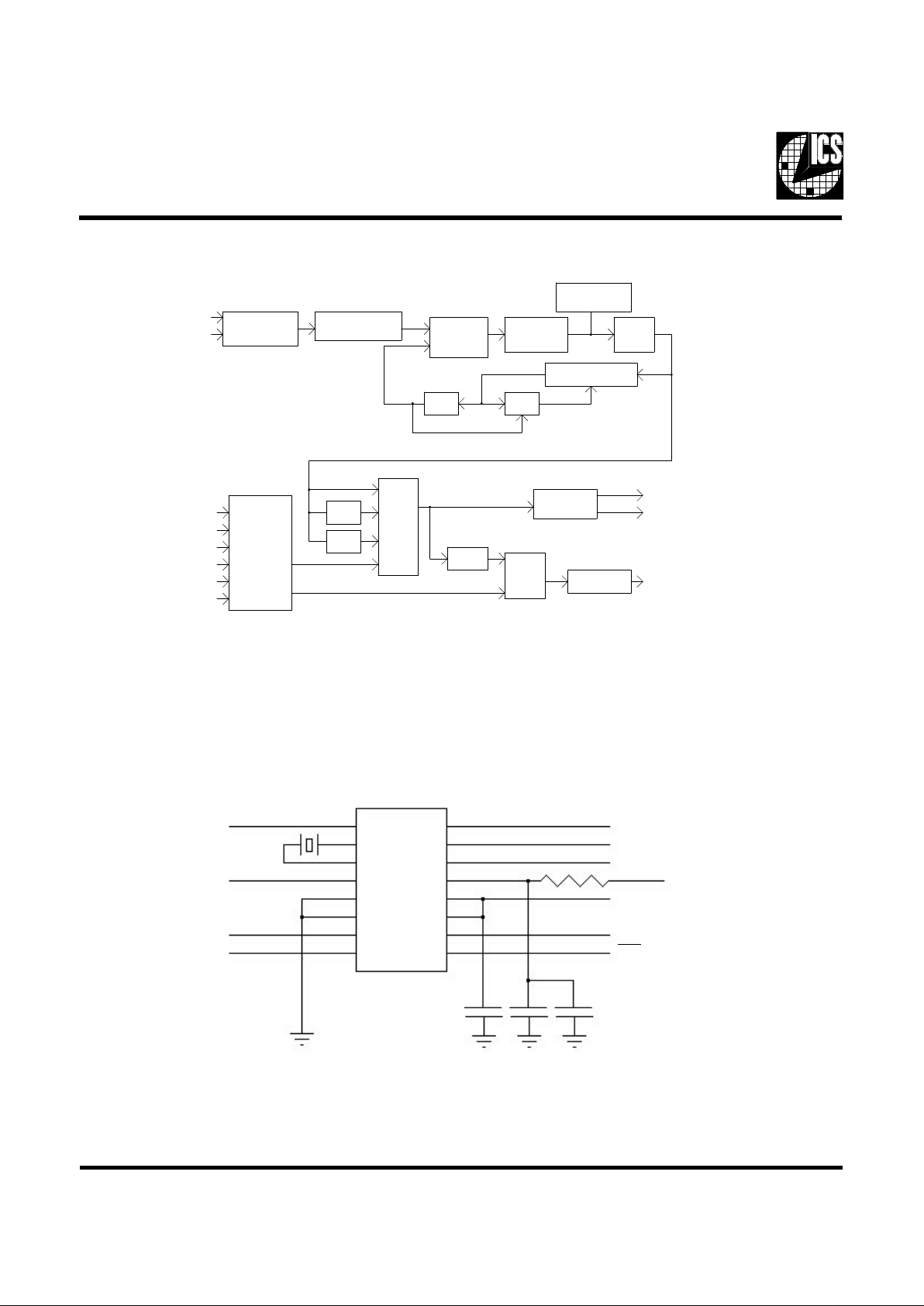
Figure 1
System Schematic
116
215
314
413
512
611
710
89
FS0
XT AL
STROBE
LOAD
FS4
V
SS
FS1
FS2
FS3
V
DD
10
CLK
CLK
V
DDO
C3.1C2.1C1+
22
ICS1567
Figure 2
Block Diagram
ICS1567
2
Page 3
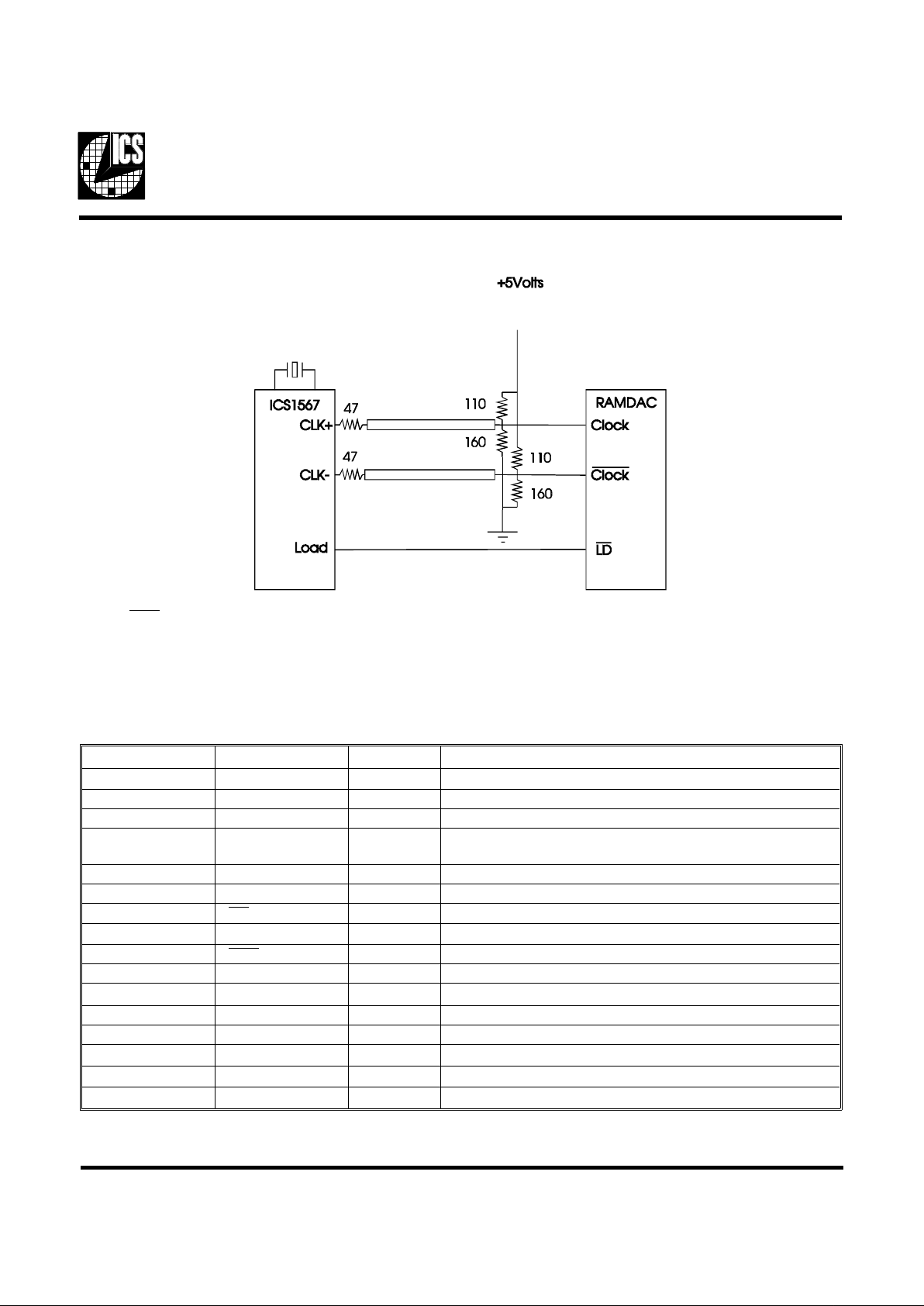
Typical Output Configuration
Pin Description
PIN NUMBER PIN SYMBOL TYPE DESCRIPTION
1
• FS0
IN
Frequency Select LSB.
2
XTAL1
IN
Crystal Inte rfa ce /E xter na l Oscill a tor Input .
3
XTAL2
OUT
Crystal Inte rfa ce .
4
• STROBE
IN
Control Fo r Frequency Sel e ct Lat ch , also performs automati c
RAMDAC reset.
5
VSS
--
Device Ground (Both pins mu st be conne cte d.)
6
VSS
--
Device Ground (Both pins mu st be conne cte d.)
7
LD
OUT
Load Output. This output is at CL K fre quency divi de d by N 1 .
8
• FS4
IN
Frequency Select MSB.
9
CLK
OUT
Clock Out put Inve rt ed .
10
CLK
OUT
Clock Output Non-In ve rted.
11 VDDO
--
Output Stage Powe r (Bot h pins must be conn ect ed ).
12
VDDO
--
Output Stage Powe r (Bot h pins must be conn ect ed ).
13
VDD
--
PLL System Power.
14
• FS3
IN
Frequency Select.
15
• FS2
IN
Frequency Select.
16
• FS1
IN
Frequency Select.
• = inputs with internal pull- up re sisto r
Notes:
CLK &
CLK outputs are pseudo-ECL. Logic low level is set by the ratio of the resistor s stacked acr o s s the power suppl y
V
LO
= (V suppl y • 160)/(110 +160) in the example shown above.
The above val ue s are a good sta rt in g poi nt fo r RAMDAC or clo ck gen er at or i nte rf ac e .
Figure 3
ICS1567
3
Page 4

Circuit Description
Overview
The ICS1567 is design ed to provide the gra phics system clock
signals require d by industry standa rd RAMDACs. One of 32
pre-progr amm ed (user -de fina ble) freque nci es ma y be sel ecte d
under digital control. Fully programmable feedback and reference divider capability allow virtually any frequency to be
genera ted, n ot just simpl e m ultip les of the re fere nce freque ncy.
The ICS1567 uses the latest ge neration of fre quency synthesis
technique s deve loped b y ICS and is comp letel y suitabl e for the
most dem an din g vid eo app li ca tions.
Digital Inputs
The FS0-FS4 pins and the STROB E pin are used to select the
desired ope ra ting fr eq ue nc y fro m the 32 pr e- prog ra mme d f requencies in the ROM tabl e of the ICS1567. The STR OBE pi n
also controls activation of the pipeline delay RESET function
included in the ICS1567 (see PIPELINE DELAY RESET
section for details). The FS0 -FS4 and STROBE pins are each
equipped wit h a pull-up and will be at a logic HIGH level whe n
not connected.
Transpa rent Mode - When the STROBE pin is held HIGH,
the FS0 through FS4 inputs are transparent; that is, they directly access the ROM table. The synthesizer will output the
frequency programmed into the location addressed by the
FS0-FS4 pins.
Latched Mode - When the STROBE pin is held LOW, the
FS0-FS4 pins are ignored. The synthesizer will output the
frequency correspon ding t o the st ate of t he FS0-FS4 pins when
the STROB E pin was last H IGH. In the event tha t the ICS1567
is powered-up with the STROBE pin held LOW, the synthesizer wi ll output t he frequ ency pro grammed into add ress 0 (i .e.,
the one selected wit h FS0 throug h FS4 at a log ic LOW level).
Frequency Synthesizer Description
Refer to Figure 1 for a block diagram of the ICS1567. The
refere nce freque nc y i s gen erated by an o n-chip crysta l osci ll ator , or the re ferenc e fr eq uency may be appli e d to the ICS156 7
from an external frequency source.
The ICS1567 generates its output frequencies using phaselocked loop techniques. The phase-locked loop (or PLL) is a
closed-loop feedback system that drives the output frequency
to be rati ometrical ly related to th e reference frequency pr ovided
to the PLL. The phase -fre qu en cy detector sh own in th e bloc k
diagram drive s the VCO to a frequency that wi ll cause the two
inpu ts t o t he phas e-freq uen cy de tec tor t o b e ma tched in frequency a nd phase. This oc curs when:
F(XTAL1) • Feedback Divider
F(vco) =
Reference Divider
This expression is exact; that is, the accuracy of the output
frequen cy depends sol e ly on the re fe rence frequency provided
to the part (assuming correctly-programmed dividers). The
divider progr amm in g is one of the fu ncti ons pe rfor med by the
ROM look-up table in the ICS1567. The VCO gain is also
ROM programmable which permits the ICS1567 to be optimized for be st performa nc e a t ea ch fre que ncy in the tabl e.
The feedback divider makes use of a dual-modulus prescaler
technique that allows construction of a program ma ble count e r
to operate at high speeds while still allowing the feedback
divider to be progr ammed in steps of 1. This is an improvement
over conventional fixed prescaler architectures that typically
impose a factor -of -fou r pena lt y (or lar g er) in this respect.
A p ost-divide r may b e insert ed betwe en the VCO and t he CLK
and
CLK outputs of the ICS1567. This is useful in generation
of lower frequencies, as the VCO has been optimized for
high-frequency ope ration. Different post-divide r settings m a y
be used for each frequenc y in the table.
ICS1567
4
Page 5

Load Clock Divider
The ICS1567 has an additional programmable divider that is
used to generate the LOAD frequency. The modulus of this
divider may be set to 3, 4, 5, 6, 8, or 10. The design of this
divider permits the output duty factor to be 50/50, even whe n
an odd modulus is sel e ct e d.
The selection of the modulus is done by the ROM look-up
table. A different modulus may, therefore, be selected for each
freq ue ncy addres s.
Pipeline Delay Reset Function
The ICS1567 implements the clocking sequence required to
reset the pipeline delay on Brooktree RAMDACs. This sequen ce i s a uto ma tica lly g ener ate d by th e ICS1567 upon any
rising edge of t he STRO B E line.
When the frequency select inputs (FS0-FS4) are used in a
transparen t mode, simpl y lower and raise th e STROBE line to
activate the function. When the frequency select inputs are
latched, simply load the same frequency into the ICS1567
twice.
When changing frequencies, it is advisable to allow 500uSec
after the new frequency is selected to activate the reset function. The outp ut fr eq uency of the synt he siz e r sh oul d be stable
enough at that point for the RAMDAC to correctly execute its
reset sequence.
See Figure 4 for a diag ra m of the cl oc k seq ue nc ing .
Output Stage Description
The CL K a nd CL K ou tpu ts a re ea ch conne c ted to the d rains o f
P-Channel MOSFET devices. The source of each of these
devices is connected to VDDO. Typical on resistance of each
device is 15 Ohm s. These outputs will dri ve the clock and
clock
of a RAMDAC device when a resistive net work equ iva len t to
Figure 3 is utiliz ed .
The
LD output is a high-current CMOS type drive whose
frequen cy is controlled by a programmable di vider that may be
selecte d for a modul us o f 3, 4, 5, 6, 8, or 10. Under cont rol of
the ROM, this ou tput ma y also be suppresse d (logic low level )
at any frequ en cy sele c t addr ess, if de sire d.
Application Information
Power Supplies
The ICS1567 has two VSS pins to red uce the effe cts of package
inductance. Both pins are connected to the same potential on
the die (the ground bus). BOTH of these pins should connect
to the ground plane of the video board as close to the package
as is po ssible.
The ICS1567 has two VDDO pins which are the supply of +5
volt power to all output stages. Aga in, both VDDO pins connect
to the same point on the die. BOTH of these pins should be
connecte d to the power plane (or bus) using standa rd high-f requency de co upl ing practic e. Thi s de c oupl ing consists of a lo w
series inductance bypass capacitor, using the shortest leads
possible, mounted close to the ICS1567.
The VDD pin is the power suppl y for the synt he siz e r circui tr y
and other lower current digital functions. We recommend that
RC decou pli ng or zener re gul at io n be pro vid ed for this pi n (a s
shown in the recommended application circuitry). This will
allow the PLL to “track” through power supply fluctuations
withou t vi sible effe c ts.
Crystal Oscillator and Crystal Selection
The ICS1567 has circuitry on-board to implement a Pierce
oscillator with the addition of only one external component, a
quartz c rystal. Pi erce oscill ators ope rate the crystal i n anti- ( also
called p ar allel -) re sona nt mode . See t he AC Cha rac teri sti cs fo r
the effe ct ive cap aci tive loadin g to spec ify whe n orde ring cr ys tals.
So-called series-resonant crystals may also be used with the
ICS1567. Be aware that the oscillation frequency will be
slightly higher than the frequency that is stamped on the can
(typica lly 0. 00 5-0. 01 %).
As the entire operation of the phase-locked loop depends on
having a stable reference frequency, we recommend that the
crystal be moun ted as closely as possibl e to the packa ge. A voi d
routing digital signals or the ICS1567 outputs underneath or
near these traces. It is also desirable to ground the crystal can
to the ground plan e, if po s sible.
ICS1567
5
Page 6

Application Notes
(continued)
Bus Clock Interface
In some applications, it may be desirable to utilize the bus
clock. To do this, connect th e clock thro ugh a .047uF capa citor
to XTAL1 (2) and keep the lead length of the capacitor to
XTAL1 (2) to a minimum to reduce noise susceptibility. This
input is internally biased at VDD/2. Since TTL compatible
clocks typicall y exhi bit a VOH of 3.5V, capacitive l y coupl in g
the input restores noise immunity . The ICS1567 is not sen sitive
to the duty cycle of the bus clock; howe ver, the quali ty of this
signal varies co nsiderabl y with differe nt motherboa rd designs.
As the quality of the bus cloc k is typ ic all y outsi de the control
of the graphics adapter card manufacturer, it is suggested that
this signal be buffered on the graphics adapter board. XTAL2
(3) must be left open in this configuration.
ICS1567 Interface
The ICS1567 should be located as close as possible to the video
DAC or RAMDAC. Figure 3 illustrates interfacing the
ICS1567 to a RAMDAC. The differential output CLOCK
drivers are current sourcing only and are designed to drive
resistive terminations in a complementary fashion CLK and
CLK connections should follow good ECL interconnection
practice . T ermina ting resistors sho uld be as close as possible to
the RAMDAC.
Absolute Maximum Ratings
Ambie nt Tem e peratur e un de r bias . . . . . To. . . . . . . . . . . . . 0°C to 70°C
Supply Voltage . . . . . . . . . . . . . . . . . . . . V
DD
. . . . . . . . . . . -0.5V t o +7V
Input Voltage . . . . . . . . . . . . . . . . . . . . . . V
IN
. . . . . . . . . . . . -0.5V to V
DD
+ 0.5V
Output Voltage. . . . . . . . . . . . . . . . . . . . . V
OUT
. . . . . . . . . . -0.5V to VDD + 0.5V
Clamp Diode Current. . . . . . . . . . . . . . . . V
IK
& IOK. . . . . . ±30mA
Output Current pe r Pin. . . . . . . . . . . . . . . I
OUT
. . . . . . . . . . . ±50mA
Stora g e Temperature . . . . . . . . . . . . . . . . T
S
. . . . . . . . . . . . . -85°C to + 150°C
Power Dissipation . . . . . . . . . . . . . . . . . . P
D
. . . . . . . . . . . . . 500mW
Values beyond these ratings may damage the device. This device contains circuitry to protect the inputs and outputs against
damag e due to high static vol tages or elec tric fie lds; howeve r, it is advised that norma l precaut ions be taken to avoid applica tions
of any voltage higher than the max imum rated volta ges. For proper ope ration, it is recomm ended that V
IN
and V
OUT
be constra ined
to > = V
SS
and < = VDD.
Standard Test Conditions
The characteristics below apply for the following standard test conditions, unless otherwise noted. All voltages are referenced
to VSS (OV Ground). Positiv e curr en t flows into th e ref eren ce d pin.
Operati ng Temperatur e range
0°C to 70°C
Power supply volta ge 4.75 to 5.25 Volts
ICS1567
6
Page 7

DC Characteristics
PARAMETER SYMBOL MIN MAX UNITS CONDITIONS
Input High Voltage V
IH
2.0 VDD + 0.5 V
Input Low Voltage V
IL
VSS -0.5 0.8 V
Input High Current I
IH
10 uA VIN = V
DD
Input Low Current I
IL
-200 uA VIN = V
SS
LOAD OUTPUT
Output High Voltage V
OH
2.4 V IOH = -4 . 0 mA
Output Low Voltage V
OL
0.4 V IOL = 6.0 mA
CLOCK OUTPUTS
Differentia l Output Voltage
(CLK-
CLK)
V
OD
1.2 V See Figure 4
XTAL1 INPUT
Input High Voltage V
XH
3.75 VDD + 0.5 V
Input Low Voltage V
XL
VSS -0.5 1.25 V
Operating Curre nt I
DD
50 mA Outputs Unl oa de d
Input Pin Capacitanc e C
IN
8pFF
C
= 1 MHz
Output Pin Capacitanc e C
OUT
12 pF FC = 1 MHz
ICS1567
7
Page 8

AC Characteristics
PARAMETER SYMBOL MIN TYP MAX UNITS
NOTES
CLK and CLK T IMING
Duty Cycle
T
HIGH
40 60 % 3, 4, 9
Frequency E rror
0.5 %
Rise Time
T
r
2ns5, 9
Fall Ti me
T
f
2ns5, 9
VCO Frequency
F
VCO
20 180 MHz 1
PLL Acqui re T i me
T
LOCK
500 uS
LD* TIMING
Duty Cycle
T
HIGH
40 60 % 6
Load Frequency
F
LOAD
60 MHz
Rise Time
T
r
2ns7, 8
Fall Ti me
T
f
2ns7, 8
REFERENCE INPUT CLOC K
Crystal Frequency
F
XTAL
520MHz
Crystal Oscillator
C
PAR
20 pF
Loading Capa ci tance
XTAL1 High Time
T
XHI
8ns2
XTAL1 Low Time
T
XLO
8ns2
Rise Time
T
r
10 ns 2, 7
Fall Ti me
T
f
10 ns 2, 7
DIGITAL INPUTS
Frequenc y Sele c t Set up Time
110 ns10
Frequenc y Sele ct Ho ld Time
210 ns10
Strobe Pulse Width
320 ns10
PIPELINE DELAY RESET
Reset Acti vati on
42*T
CLK
ns 10
Reset Duration
5 4*T
CLK
ns 10
Rest a r t D e lay
6 -1*T
CLK
+1.5*T
CLK
ns 10
Notes:
1. Use of the post-d ivi de r is re qui re d for frequencies lowe r tha n 20 MHz on CL K and
CLK outputs. Use of the
post-divider i s recom m en ded for ou tpu t fre qu en cie s lowe r than 65 MHz.
2. Values for XTAL1 driven by an external clock
3. Duty Cycle for Dif fe re ntia l Output (CL K-
CLK)
4. Duty cycle measured at VOD/2 for Dif fere nt ial CLK Outp ut
5. Rise and fall time between 20% an d 80% of VO D
6. Duty cycle measured at 1.4V for T TL I/O
7. Rise and fa ll tim e between 0.8 and 2. 0 VD C for T TL I/O
8. Output pin loading = 15 pF
9. See Figure 3.
10. See Figure 4.
ICS1567
8
Page 9

LATCHED INPUTS:
3
STROBE
FS0-FS4
12
33
4
5
6
Tclk
STROBE
DIFF CLK
LD
Figure 4
PIPELINE DELAY RESET:
ICS1567
9
Page 10

ICS1567 Pattern Request Form
Custom patt erns are also a vailable, a lt hough a signif ic ant volume commitment and/or one-time mask charge will apply.
Contact ICS Sa les for de t ai ls.
ICS Pa rt
Number
ICS1567-
742
ICS1567-
Cust om Pattern #1
Vi de o Cl ock
Address (HEX)
Frequency
(MHz)
Frequency
(MHz)
0 112.000
1 148.000
2 OFF
3 135.000
4 31.500
5 105.500
6 78.000
7 86.000
8 108.000
9 120.000
10 128.000
11 93.000
12 112.000
13 148.000
14 135.000
15 89.210
16 105.500
17 112.000
18 25.000
19 45.000
20 64.000
21 75.000
22 78.000
23 86.000
24 103.000
25 108.000
26 120.000
27 127.000
28 128.000
29 135.000
30 112.000
31 148.000
Custom pattern #1 refe renc e freq uenc y = ______ ____ ___
Standard pattern shown above uses 16.000 MHz as the input
reference frequency.
ICS1567
10
Page 11

Figure 5: 16-Pin SOIC Package
LEAD COUNT 16L
DIMENSION L .404
Ordering Information
ICS1567M-XXX
Example:
ICS XXXX M -XXX
Pattern Number (2 or 3 digit numbe r for parts with ROM c ode patterns )
Package Type
M=SOIC
Device Type (cons ist s of 3 or 4 digit num be rs )
Prefix
ICS, AV=Stan dard Device ; GSP=Genloc k Device
ICS1567
11
 Loading...