

ICST GSP9108-10CS8, GSP9108-10CS14, GSP9108-10CN8, GSP9108-10CN14, GSP9108-05CS8 Datasheet
...
Integrated
Circuit
Systems, Inc.
AV9108
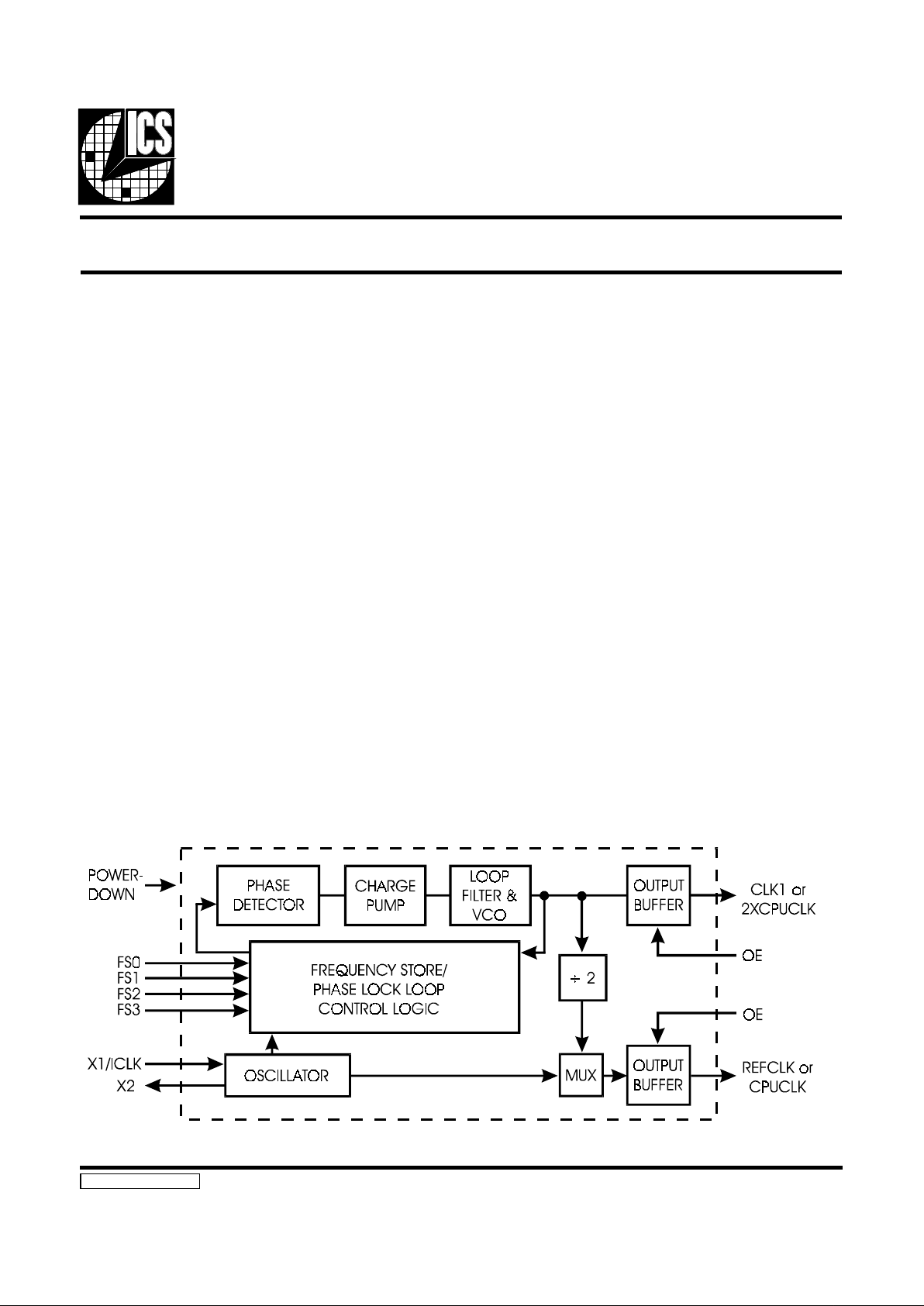
CPU Frequency Generator
Block Diagram
AV 9108 RevB032195
General Description
The AV9108 offers a tiny footprint solution for generating two
simultaneous clocks. One clock, the REFCLK, is a fixed output
frequency which is the same as the input reference crystal (or
clock). The other clock, CLK1, can vary between 2 and 120
MHz, with up to 16 selectable preprogrammed frequencies
stored in internal ROM.
The ICS9108 is ideal for use in a 3.3V system. It can generate
a 66.66 MHz clock at 3.3V. In addition, the ICS9108 provides
a symmetrical wave form with a worst case duty cycle of 45/55.
The ICS9108 has very tight edge control between the CPU
clock and 2XCPU clock outputs, with a worst case skew of
250ps.
The device has advanced features which include on-chip loop
filters, tristate outputs, and power-down capability. A minimum of external components - two decoupling capacitors and
an optional ferrite bead - are all that are required for jitter-free
operation. Standard versions for computer motherboard applications are the AV9108-03, AV9108-05 and the ICS9108-10.
Custom masked versions, with customized frequencies and
features, are available in 6-8 weeks for a small NRE fee.
Features
•• Runs up to 80 MHz at 3.3V
•• 50/50 typical duty cycle at 5V
••±250ps absolute jitter
•• Generates frequencies from 2 to 140 MHz
•• 2 to 32 MHz input reference frequency
•• Up to 16 frequencies stored internally
•• Patented on-chip Phase Locked Loop with VCO for clock
generation
•• Provides reference clock and synthesized clock
•• On-chip loop filter
•• Low power 0.8µ CMOS technology
•• 8-pin or 14-pin DIP or SOIC package
Pin Configuration
Pin Descriptions for
AV9108-03, AV9108-05 and AV9108-10
PIN NUMBER PIN
NAME TYPE DESCRIPTION
-05/-10/-13 -03
1 14 FS0 Input Frequency Select 0 for CLK1 (-03 has pull-up).
5 1 FS1 Input Frequency Select 1 for CLK1 (-03 has pull-up).
2 FS2 Input Frequency Select 2 for CLK1 (-03 has pull-up).
3 FS3 Input Frequency Select 3 for CLK1 (-03 has pull-up).
4 AGND - Analog GROUND.
2 5 GMD - Digital GROUND.
6
PD Input POWER-DOWN. Shuts off chip when low. Internal pull-up.
3 7 X1/ICLK Input CRYSTAL OUTPUT or INPUT CLOCK frequency. Typically 14.318 MHz
system clock.
4 8 X2 Output CRYSTAL OUTPUT (No Connect when clock used.).
9 OE(REFCLK) Input OUTPUT ENABLE. Tristates REFCLK when low. Pull-up.
10 OE(CLK1) Input OUTPUT ENABLE. Tristates CLK1 when low. Pull-up.
6 11 CLK1 Output CLOCK1 Output (see decoding tables).
7 12 VDD - Digital power supply (+3V DC).
8 13 REFCLK Output REFERENCE CLOCK output. Produces a buffered version of the input clock or
crystal frequency (typically 14.318 MHz).
FS0 1 8 REFCLK
GND 2 7 VDD
X1/ICLK 3 6 CLK1
X2 4 5 FS1
AV9108-05/-10
8-Pin DIP, SOIC
FS1 1 14 FS0
FS2 2 13 REFCLK
FS3 3 12 VDD
AGND 4 11 CLK1
GND 5 10 OE (CLK1)
PD 6 9 OE (REFCLK)
X1/ICLK 7 8 X2
AV9108-03/-11
14-Pin DIP, SOIC
AV9108
2
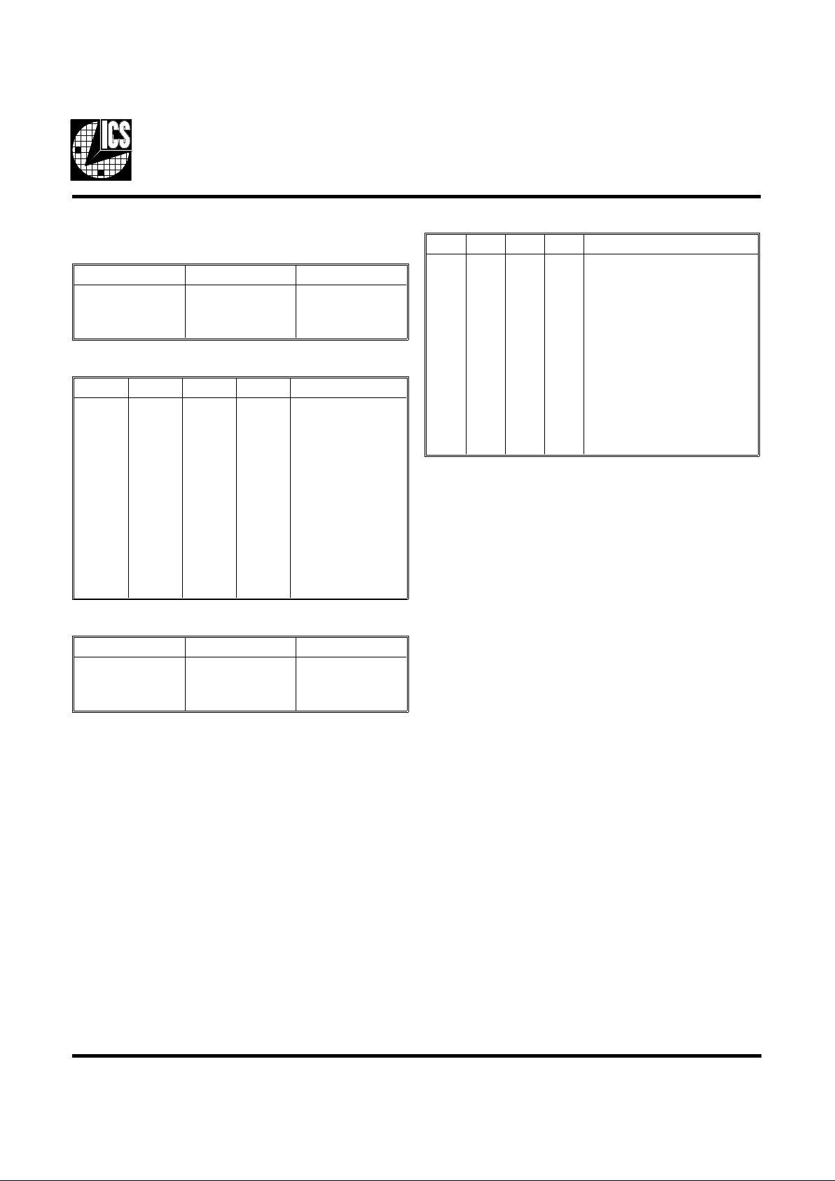
Actual Frequencies
Decoding Table for AV9108-05, 14.318 input
FS1 FS0 CLK1
0
0
1
1
0
1
0
1
40.01 MHz
50.11 MHz
66.61 MHz
80.01 MHz
Decoding Table for AV9108-03, 14.318 input
FS3 FS2 FS1 FS0 CLK1
0
0
0
1
0
0
0
0
1
1
1
1
1
1
1
1
0
0
0
0
1
1
1
1
0
0
0
0
1
1
1
1
0
0
1
1
0
0
1
1
0
0
1
1
0
0
1
1
0
1
0
1
0
1
0
1
0
1
0
1
0
1
0
1
16.00 MHz
39.99 MHz
50.11 MHz
80.01 MHz
66.58 MHz
100.23 MHz
8.02 MHz
4.01 MHz
8.02 MHz
20.00 MHz
25.06 MHz
40.01 MHz
33.29 MHz
50.11 MHz
4.01 MHz
2.05 MHz
Decoding Table for AV9108-10, 14.318 input
FS1 FS0 CLK1
0
0
1
1
0
1
0
1
25.057 MHz
33.289 MHz
40.006 MHz
50.113 MHz
Decoding Table for AV9108-11 (in MHz)
FS3 FS2 FS1 FS0 CLK1
0
0
0
1
0
0
0
0
1
1
1
1
1
1
1
1
0
0
0
0
1
1
1
1
0
0
0
0
1
1
1
1
0
0
1
1
0
0
1
1
0
0
1
1
0
0
1
1
0
1
0
1
0
1
0
1
0
1
0
1
0
1
0
1
16.00 MHz
33.39 MHz
50.11 MHz
80.01 MHz
66.58 MHz
100.23 MHz
60.00 MHz
4.01 MHz
8.02 MHz
20.05 MHz
25.06 MHz
39.99 MHz
33.25 MHz
50.11 MHz
30.00 MHz
4.01 MHz
Note: The dash number following ICS9108 must be included when ordering product since it specifies the frequ ency decoding
table being ordered. Decoding options can be created by a simple metal mask change.
AV9108
3

Frequency Accuracy and Calculation
The accuracy of the frequencies produced by the ICS9108
depends on the input frequency and the desired actual output
frequency. The formula for calculating the exact frequency is
as follows:
A
Output Frequency = Input Frequency ×
B
where A=2, 3, 4 ... 128, and
B=2, 3, 4 ... 32.
For example, to calculate the actual output frequency for a
video monitor expecting a 44.900 MHz clock and using a
14.318 MHz input clock, the closest A/B ratio is 69/22, which
gives an output of 44.906 MHz (within 0.02% of the target
frequency). Generally, the ICS9108 can produce frequencies
within 0.1% of the desired output.
Allowable Input and Output Frequencies
The input frequency should be between 2 and 32 MHz and the
A/B ratio should not exceed 24. The output should fall in the
range of 2-120 MHz.
Output Enable
The Output Enable feature tristates the specified output clock
pins. This places the selected output pins in a high impedance
state to allow for system level diagnostic testing.
Power-Down
If equipped, the power-down shuts off the specified PLL or
entire chip to save current. A few milliseconds are required to
reach full functioning speed from a power-down state.
Frequency Transitions
A key ICS9108 feature is the ability to provide glitch-free frequency transitions across its output frequency range. The ICS9108
provides smooth transitions between any of the two groups of eight frequencies (when FS3=0 or FS3=1), so that the device will
switch glitch-free between 4-100 MHz and 2-50 MHz.
AV9108
4

Absolute Maximum Ratings
AVDD, VDD referenced to GND. . . . . . . . . . . . . . . 7V
Operating temperature under bias. . . . . . . . . . . . . . . . 0°C to +70°C
Storage temperature. . . . . . . . . . . . . . . . . . . . . . . . . . -65°C to +150°C
Voltage on I/O pins referenced to GND. . . . . . . . . . . GND -0.5V to VDD +0.5V
Power dissipation. . . . . . . . . . . . . . . . . . . . . . . . . . . . 0.5 Watts
Stresses above those listed under Absolute Maximum Ratings may cause permanent damage to the device. This is a stress rating
only and functional operation of the device at these or any other conditions above those indicated in the operational sections of
the specifications is not implied. Exposure to a bsolute maximum rating conditions for extende d periods may affect product
reliability.
Electrical Characteristics at 5V
(Operating VDD = +4.5V to +5.5V; TA =0°C to 70°C unless otherwise stated)
DC Characteristics
PARAMETER SYMBOL TEST CONDITIONS MIN TYP MAX UNITS
Input Low Voltage V
IL
--0.8V
Input High Voltage V
IH
2.0 - - V
Input Low Current I
IL VIN
=0V - 6.0 16 µA
Input High Current I
IH VIN=VDD
-2.0 - 2.0 µA
Output Low Voltage V
OL IOL
=10mA - 0.15 0.40 V
Output High Voltage, Note 1 V
OH IOH
=-30mA 2.4 3.25 - V
Output Low Current, Note 1 I
OL VOL
=0.8V 22.0 35.0 - mA
Output High Current, Note 1 I
OH VOH
=2.0V - -50.0 -35.0 mA
Supply Current I
CC
Unload, 50 MHz - 18.0 42.0 mA
Supply Current I
CC
(PD low)
Unload, Logic Inputs 000 - 38.0 100.0 µA
Supply Current I
CC
(PD low)
Unload, Logic Inputs 111 - 14.0 40.0 µA
Pull-up Resistor, Note 1 R
pu
- 380.0 700.0 k ohms
AC Characteristics
Rise Time 0.8 to 2.0V, Note 1 T
r
15pf load - 0.60 1.40 ns
Fall Time 2.0 to 0.8V, Note 1 T
f
15pf load - 0.40 1.00 ns
Rise Time 20% to 80%, Note 1 T
r
15pf load - 2.0 3.5 ns
Fall Time 80% to 20%, Note 1 T
f
15pf load - 1.0 2.5 ns
Duty Cycle, Note 1 D
t
15pf load @ 1.4V 45.0 50.0 55.0 %
Jitter, One Sigma, Note 1 T
jis
From 20 to 100 MHz - 50.0 150.0 ps
Jitter, One Sigma, Note 1 T
jis
From 14 to 16 MHz 100.0 200.0 ps
Jitter, One Sigma, Note 1 T
jis
From 14 to Below 0.2 1.0 %
Jitter, Absolute, Note 1 T
jab
From 20 to 100 MHz -250.0 250.0 ps
Jitter, Absolute, Note 1 T
jab
From 14 to 16 MHz -500.0 500.0 ps
Jitter, Absolute, Note 1 T
jab
From 14 to Below 1.0 3.0 %
Input Frequency, Note 1 F
i
11.0 14.3 19.0 MHz
Output Frequency F
o
2.0 - 120.0 MHz
Power-up Time, Note 1 T
pu
-7.5818.0ms
Transition Time, Note 1 T
ft
8 to 66.6 MHz - 6.0 13.0 ms
Note 1: Parameter is guaranteed by design and characterization. Not 100% tested in production.
AV9108
5

Electrical Characteristics at 3.3V
(Operating VDD = +3.0V to +3.7V; TA =0°C to 70°C unless otherwise stated)
DC Characteristics
PARAMETER SYMBOL TEST CONDITIONS MIN TYP MAX UNITS
Input Low Voltage V
IL
- - 0.20V
DD
V
Input High Voltage V
IH
0.7V
DD
--V
Input Low Current I
IL VIN
=0V - 2.5 7.0 µA
Input High Current I
IH VIN=VDD
-2.0 - 2.0 µA
Output Low Voltage V
OL IOL
=6mA - 0.15 0.1 V
Output High Voltage V
OH IOH
=-5mA 0.85 0.92 - V
Output Low Current I
OL VOL
=0.2V
DD
15.0 22.0 - mA
Output High Current I
OH VOL
=0.7V
DD
- -17.0 -10.0 mA
Supply Current I
CC
Unloaded, 50 MHz - 22.0 40.0 mA
Supply Current I
CC
(PD low)
Unload, Logic Inputs 000 - 13.0 40.0 µA
Supply Current I
CC
(PD low)
Unload, Logic Inputs 111 - 4.0 12.0 µA
Pull-up Resistor R
pu
- 550.0 900.0 k ohms
AC Characteristics
Rise Time 20% to 80%, Note 1 T
r
15pf load - 2.2 3.5 ns
Fall Time 80% to 20% T
f
15pf load - 1.2 2.5 ns
Duty Cycle D
t
15pf load @ 50% 40.0 46.0 60.0 %
Jitter, One Sigma T
jis
From 25 to 85 MHz - 50.0 150.0 ps
Jitter, One Sigma T
jis
From 14 to 20 MHz 100.0 200.0 ps
Jitter, One Sigma T
jis
From 14 to Below 0.4 1.0 %
Jitter, Absolute T
jab
From 25 to 85 MHz -250.0 250.0 ps
Jitter, Absolute T
jab
From 14 to 20 MHz -500.0 500.0 ps
Jitter, Absolute T
jab
From 14 to Below 1.0 3.0 %
Input Frequency F
i
13.3 14.3 15.3 MHz
Output Frequency F
o
2.0 - 90.0 MHz
Power-up Time, Note 1 T
pu
- 7.58 18.0 ms
Transition Time, Note 1 T
ft
8 to 66.6 MHz - 6.0 13.0 ms
Parameter is guaranteed by design and characterization.
AV9108
6

8-Pin DIP Package
14-Pin DIP Package
Ordering Information
AV9108-XXCN8, ICS9108-XXCN14
Example:
XXX XXXX- XX M X#W
Lead Count & Package Width
Lead Count=1, 2 or 3 digits
W=.3” SOIC or .6” DIP; None=Standard Width
Package Type
N=DIP (Plastic)
Pattern Number (2 or 3 digit number f or parts w ith ROM code patterns)
Device Type (consists of 3 or 4 digit numbers)
Prefix
ICS, AV=Standard Device; GSP=Genlock Device
AV9108
7

8-Pin Plastic SOIC
14-Pin SOIC Package
Ordering Information
ICS9108-XXCS8, IS9108-XXCS14
Example:
XXX XXXX- XX M X#W
Lead Count & Package Width
Lead Count=1, 2 or 3 digits
W=.3” SOIC or .6” DIP; None=Standard Width
Package Type
S=SOIC
Pattern Number (2 or 3 digit number f or parts w ith ROM code patterns)
Device Type (consists of 3 or 4 digit numbers)
Prefix
ICS, AV=Standard Device; GSP=Genlock Device
AV9108
8
 Loading...