Integrated
Circuit
Systems, Inc.
General Description Features
AV9107C-13
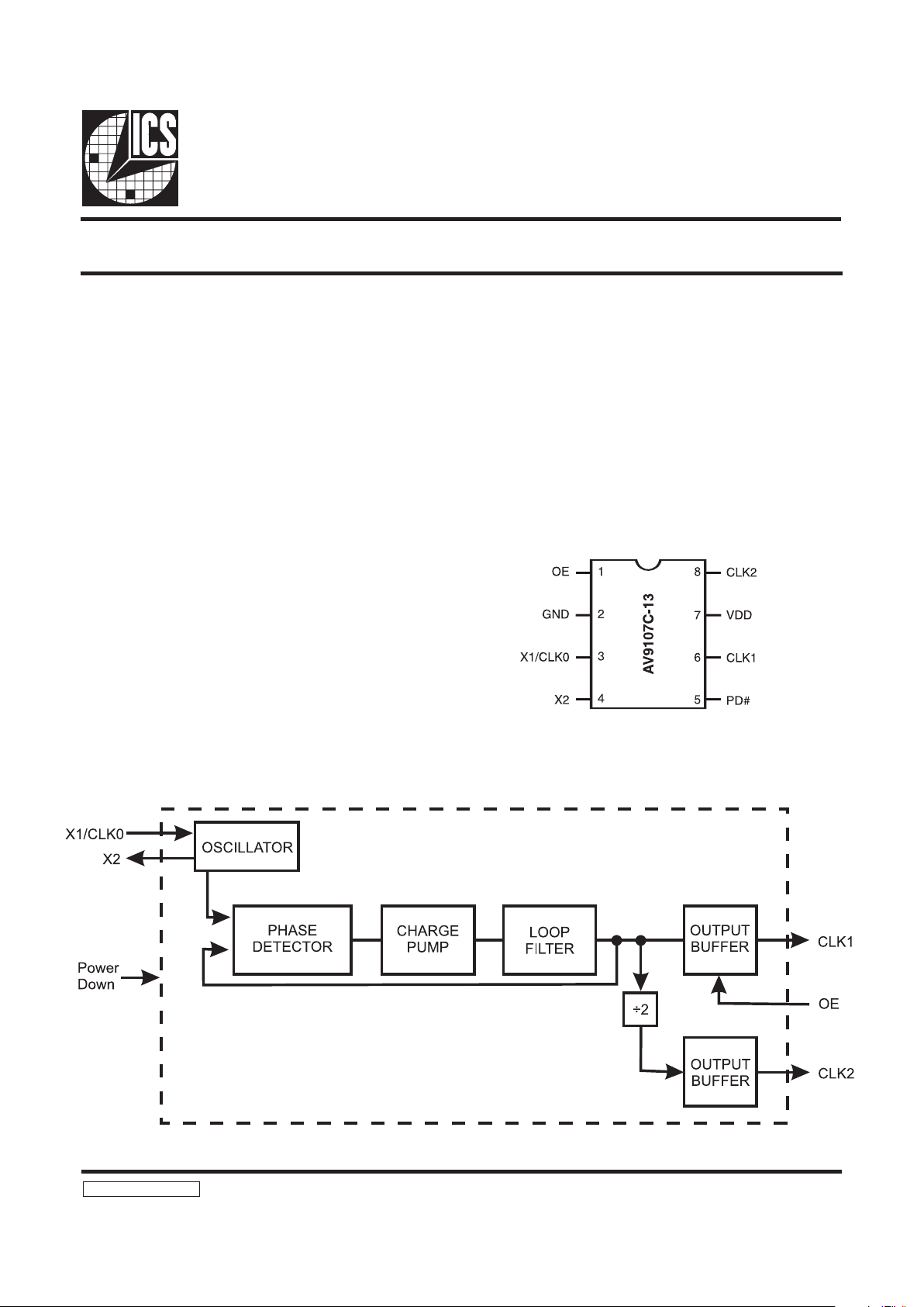
Block Diagram
CPU Frequency Generator
AV 9107-13 RevB052197
The AV9107C-13 offers a tiny footprint solution for
generating two simultaneous clocks. The AV9107C-13
uses a 20 MHz crystal to generate two PLL synthesis
outputs of 20 and 40 MHz. The Output enable pin will
tristate the 40 MHz output when low (maintaining the 20
MHz output runing in both logic levels). The power pin
takes the device to a low current condition, shutting off the
PLL and forcing both outputs low, when the PD# pin is low.
There is a built-in pull-up on both the OE and PD# inputs.
The device has advanced features which include on-chip
loop filters, tristate outputs, and power-down capability. A
minimum of external components - two decoupling capacitors
and an optional ferrite bead - are all that are required for jitterfree operation.
Patented on-chip Phase-Locked Loop with VCO
for clock generation
Provides two synthesized clocks
Generates 20 and 40 MHz output frequencies.
On-chip loop filter
Low power CMOS technology
Single +3.3 or +5 volt power supply
8-pin SOIC package
Pin Configuration
Note: Crystal is 20 MHz

2
AV9107C-13
Pin Descriptions
Functionality
(at 14.318) MHz reference frequency input)
Frequency Accuracy and Calculation
The accuracy of the frequencies produced by the AV9107C
depends on the input frequency and the desired actual
output frequency. The formula for calculating the exact
output frequency is as follows:
For example, to calculate the actual output frequency for
a video monitor expecting a 44.900 MHz clock and using
a 14.318 MHz input clock, the closest A/B ratio is 69/22,
which gives an output of 44.906 MHz (within 0.02% of the
target frequency). Generally, the AV9107 can produce
frequencies within 0.1% of the desired output.
PIN
NUMBER
PIN NAME TYPE DESCRIPTION
1 OE Input Output Enable - Tristates the 40 MHz output when low. Pull-Up
2 GND PWR Ground.
3 X1/CLK0 Input Crystal Input or Input Clock frequency. Typically 20MHz crystal.
4 X2 Output Crystal Output (No Connect wh en clock used.).
5 PD# Input Power Down. Shuts off chip when low outputs are driven low. Internall pull-up.
6 CLK1 Output Clock 1 output 40MHz with 20MHz crysta l.
7 VDD PWR Digital power supply (+5V DC).
8 CLK2 Output
Clock2 output, div ided by 2 from clo ck1 output, for 20 MHz with 20MHz c rystal. Output is
synthesized.
OE CLK1 CLK2
0 20 MHz Tristate
1 20 MHz 40 MHz
Output Frequency = Input Frequency X
A
B
Allowable Input and Output Frequencies
The input frequency should be between 12 and 40 MHz
and the A/B ratio should not exceed 24. The output should
fall in the range of 12 to 80 MHz for CLK1 dnd CLK2. (See
specification for 3.3V and 5V condition details).
Output Enable
The Output Enable feature tristates the CLK1 output clock
pin. This places the selected output pins in a high inpedance
state to allow for system level diagnostic testing. The divideby-2 output of CLK2 remains active on the AV9107C-13 for
any OE state.
Power Down
The power down pin shuts off the entire chip to save
current. A few milliseconds are required to reach full
functioning speed from a power down state.
Where
A = 2, 3, 4 ... 128, and
B = 2, 3, 4 ...32.
 Loading...