ICS82C404RevA111095
Integrated
Circuit
Systems, Inc.
ICS82C404
Advanc e Informa tion
General Description
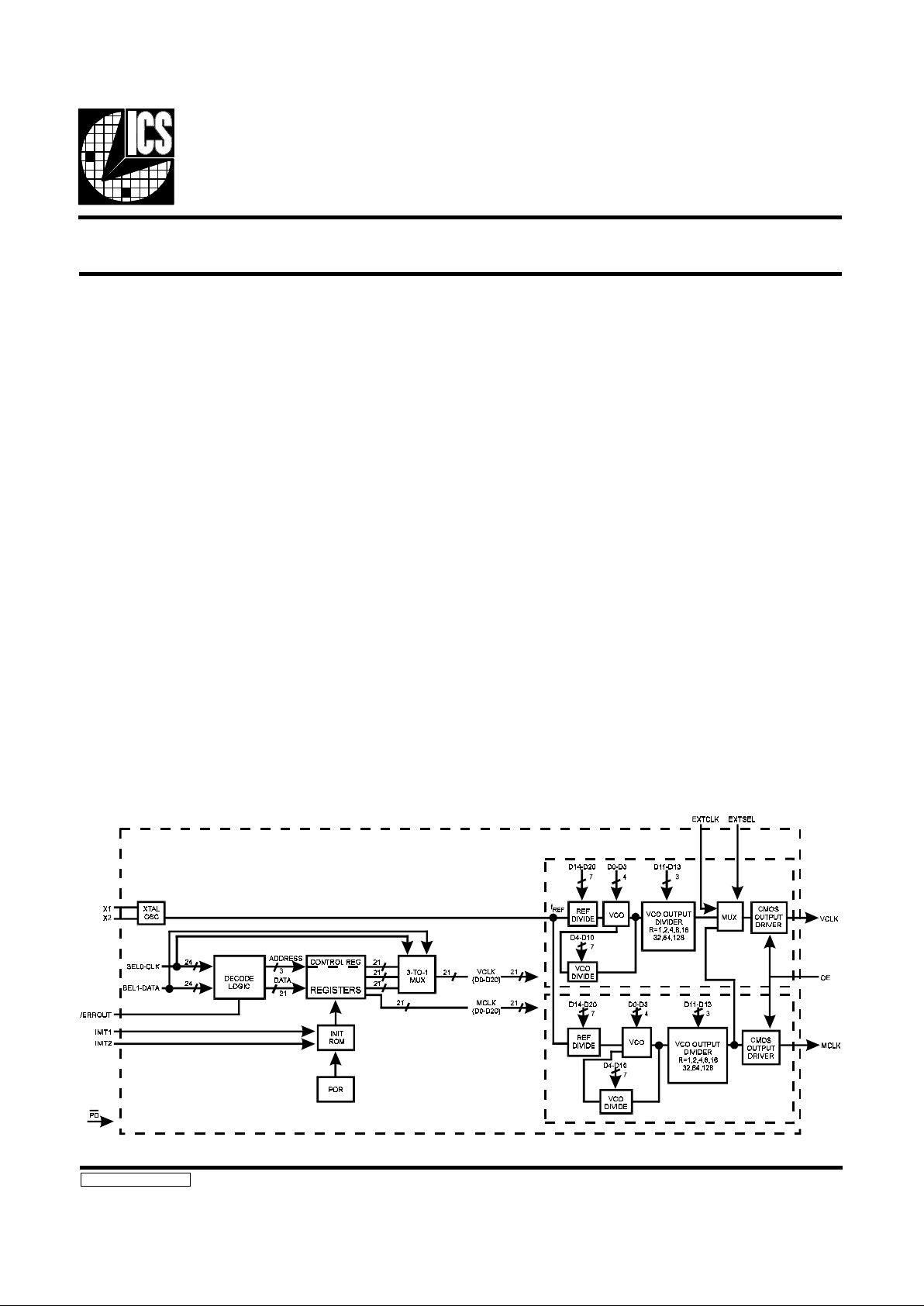
The ICS82C404 is a fully programmable graphics clock generator. It can generate user specified clock frequencies using
an exter nally generated input reference or by a single crystal.
The output frequency is programmed by entering a 24-bit
digital word through t he seri al port .
Two fully user-programmable phase-locked loops are offered
in a single packa ge. One PLL is designed to drive the mem ory
clock, while the second drives the video clock. The outputs
may be changed on-the-fly to any desired frequency between
390 kHz and 120 MHz. The ICS82C404 is ideally suited for
any desi gn whe re mult iple or varyin g freq uenc ies are require d.
This part is ideal for graphics applications. It generates low
jitter, high speed pixel clocks. It can be used to replace
multiple, expensive high speed crystal oscillators. The flexibility of the device allows it to generate non-standard graphics clock s .
The le ader in the ar ea of multip le clock ou tput clocks on a
single chip, ICS has been shipping graphics frequency generators since October, 1990, and is constantly improving the
phase-locked loop. The ICS82C404 incorporates a patented
fourth generation PLL that offers the best jitter performance
avai labl e.
Features
•• Pin-for-pin and function compatible with ICD’s version
of the 82C404
•• Dual programmable graphics clo ck generator
•• Memo ry and v ideo cloc ks are i ndivid uall y progra mm able
“on- the-f ly”
•• Ideal for designs where multiple or varying frequencies
are required
•• Increased frequency resolution from optional pre-divide-
by-2 on the M cou n te r
•• Output enable feature available for tristating outputs
•• Independent clock outputs range from 390 kHz to
120 MHz
•• Operation up to 140 MHz available
•• Power-down capabilit ies
•• Low-power , high speed 0.8 µ CMOS technology
•• Glitch-free transitions
•• Available in 16-pin PDIP or SOIC packa ge
Dual P rogram mable Graphi cs Freq uency Genera tor
Block Diagram

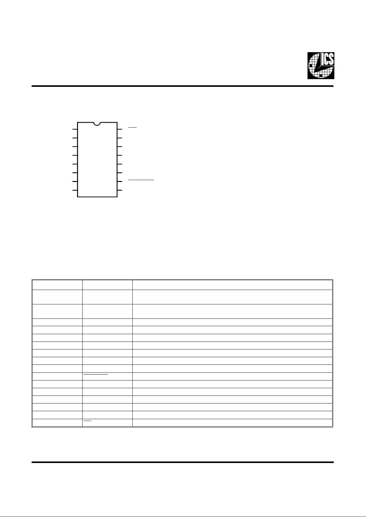
Pin Configuration
SEL0/CLK 1 16 PD
SEL1/DATA 2 15 EXTSEL
VDD 3 14 INIT1
OE 4 13 VDD
GND 5 12 INIT0
X1 6 11 EXTCLK
X2 7 10
FPMODE
MCLK 8 9 VCLK
ICS82C404
Pin Descriptions
PIN NUMBER PIN NAME DESCRIPTIO N
1 SEL 0-CL K Clock input in serial progra mm i ng m ode .
Clock select pin in operating mode.
2 SEL1-DATA Data input in serial programm ing m ode.
Clock select pin in operating mode.
3 AVDD Power.
4 OE Tri sta tes outp uts whe n lo w.
5 GND Ground.
6 X1 Crystal input.
7 X2 Crystal output.
8 MCLK Memory cloc k out put .
9 VCLK V i de o clock ou tpu t.
10
FPMODE Clock select input used to force REG2 pro gra m med fr eque nc y.
11 EXTCLK External clock input.
12 INIT0 Selects initial power-up conditions, LSB.
13 VDD Power.
14 INIT1 Selects initial power-up conditions, MSB.
15 EXTSEL Selects external clock input (EXTCLK) as VCLK output.
16
PD Power-down pin, active low.
16-Pin PDIP or SOIC
ICS82C404
2

Register Definitions
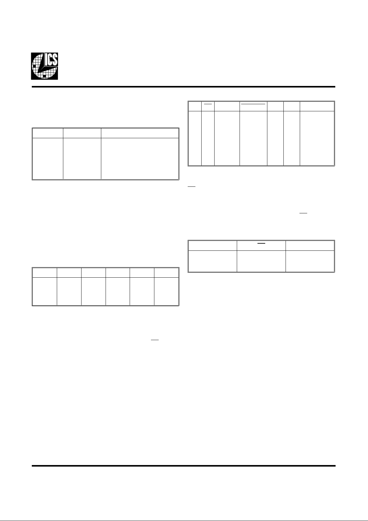
The register file c onsists of the following six registers:
Register Addr essing
Address Register Definition
000
001
010
011
100
110
REG0
REG1
REG2
MREG
PWRDWN
CNTL REG
Vi de o Cl oc k Re gist er 1
Vi de o Cl oc k Re gist er 2
Vi de o Cl oc k Re gist er 3
Memory Regist er
Divisor for Power - down m ode
Control Re gister
The ICS82C404 plac e s t he t hre e vi de o cloc k re gisters a n d t he
memory clock register in a known state upon power-up. The
regis ters are initia lized based on t he st ate of the IN IT1 a nd
INIT0 pins at applicatio n of power to the device. The INIT pins
must ramp up with VDD if a logical 1 on either pin is require d.
These input pins are inter nall y pulled d own and wi ll defa ult to
a logical 0 if left unconnected.
The registers a re initial ize d as follows:
Register Initialization
INIT1 INIT0 MREG REG0 REG1 REG2
0
0
1
1
0
1
0
1
32.500
40.000
50.350
56.644
25.175
25.175
40.000
40.000
28.322
28.322
28.322
50.350
28.322
28.322
28.322
50.350
Register Selection
When the ICS82C404 is operating, the video clock output is
control led with a comb inat ion of t he SEL 0, SEL 1,
PD, and OE
pins. The video clock is also multiplexed to an external clock
(EXTCLK) which can be selected with the EXTSEL pin. The
VCLK Select io n Table shows how VCLK is selecte d.
VCLK Selection
OE PD EXTSEL FPMODE SEL1 SEL0 VCLK
0
1
1
1
1
1
1
1
x
0
1
1
1
1
1
1
x
x
x
x
0
1
x
x
x
x
1
1
1
1
1
0
x
x
0
0
1
1
1
x
x
x
0
1
0
x
1
x
Tristate
Forced High
REG0
REG1
EXTCLK
REG2
REG2
REG2
As seen i n the table above, OE acts to tristate the outpu t. The
PD pin forces the VCLK signa l high while powering down the
part. The EXTCLK pin will only be multiplexed in when
EXTSEL and SE L 0 are logi c 0 and SE L1 is a logi c 1.
The memory clock outputs are controlled by
PD and OE as
follows:
MCLK Selection
OE PD MCLK
0
1
1
x
1
0
Tristate
MREG
PWRDWN
The Clock Selec t pins SEL0 a nd SEL 1 have two purp oses. In
serial prog ramming mod e, t hese pins act as the cl ock and data
pins. New da ta bits come in on SEL1 and t hese bits a re c locke d
in by a signal on SEL0. While these pins are acquiring new
information, the VCLK signal remains unchanged. When
SEL0 and SEL1 are acting as register selects, a time-out
interval is required t o determin e whet her t he user i s se le cting
a new register or wants to program the part. During this initial
time-out, the VCLK signal remains at its previous frequency.
At the end of this tim e -out int er va l, a ne w reg iste r i s sele c ted.
A second time-out interval is required to allow the VCO to
settle to its new value. During this period of time, typically 5 ms,
the input reference signal is multiplexed to the V CLK signal.
When MCLK or the active VCLK register is being reprogrammed, then the reference signal is multiplexed glitch-free
to the output during the first time-o ut interva l. A second timeout interva l is also re quire d to allow t he VCO to set tle. Du ring
this period, the re fere nce sign al is multipl exe d to t he a ppropri ate output signal.
ICS82C404
3

Control Register Definition
The contro l re gi ste r allo w s the user t o ad just var iou s internal option s. The re gist er is de fi ne d as fol lo w s:
Bit Bit Name Default Value Description
9
8
7
6
5
4
3
2
1
C5
C4
C3
C2
C1
C0
NS2
NS1
NS0
0
0
0
0
1
0
0
0
0
This bit determines which power -down mode the
PD pin will
implement . Power -d own mode 1, C5=0, forces the MCLK signa l to
be a function of the power- down re gi ste r. Power-d own m ode 2,
C5=1, turns of f the crysta l and disable s al l outpu ts.
This bit de te rm in es which cloc k is mu lt iplexed to VCL K duri ng
frequency changes. C4=0 multiplexes the reference frequency to the
VCLK output. C4=1 m ul ti ple xe s MCL K to th e VC LK o utput for
applic atio ns wh er e the gra phi cs c ont rol le r can not run as slow as
f
REF
.
This bit de te rm ines the len gth of the tim e- out int e rval. The tim e- out
interval is derive d fro m the MCLK VCO. If this VCO is
programme d to cert ain e xtr eme s, the time -ou t interva l maybe to o
short. C3=0, normal time-out. C3=1, doubled time -out interval.
Reserved, must be set to 0.
This bit adjust s the duty cycl e. C1=0 c a uses a 1ns dec re ase i n
output high time. C1=1 causes no adjustment. If the load
capacit ance is high, the adj ustm e nt ca n bri ng th e du ty cyc le close r
to 50%.
Reserved, must be set to 0.
Acts on register 2. NS2=0 presc a les the N cou nter by 2.
NS2=1 prescales the P counter val ue to 4.
Acts on register 1. NS1=0 presc a les the N cou nter by 2.
NS1=1 prescales the P counter val ue to 4.
Acts on register 0. NS0=0 presc a le s the P counter by 2.
NS0=1 prescales the P counter val ue to 4.
ICS82C404
4
 Loading...